US5985067A - Formation of spacers suitable for use in flat panel displays - Google Patents
Formation of spacers suitable for use in flat panel displaysDownload PDFInfo
- Publication number
- US5985067A US5985067AUS08/962,088US96208897AUS5985067AUS 5985067 AUS5985067 AUS 5985067AUS 96208897 AUS96208897 AUS 96208897AUS 5985067 AUS5985067 AUS 5985067A
- Authority
- US
- United States
- Prior art keywords
- wafer
- spacer
- firing
- spacers
- face
- Prior art date
- Legal status (The legal status is an assumption and is not a legal conclusion. Google has not performed a legal analysis and makes no representation as to the accuracy of the status listed.)
- Expired - Lifetime
Links
- 125000006850spacer groupChemical group0.000titleclaimsabstractdescription215
- 230000015572biosynthetic processEffects0.000title1
- 238000000034methodMethods0.000claimsabstractdescription119
- 238000001465metallisationMethods0.000claimsabstractdescription112
- 239000000919ceramicSubstances0.000claimsabstractdescription91
- 239000000203mixtureSubstances0.000claimsabstractdescription88
- GWEVSGVZZGPLCZ-UHFFFAOYSA-NTitan oxideChemical compoundO=[Ti]=OGWEVSGVZZGPLCZ-UHFFFAOYSA-N0.000claimsabstractdescription47
- PNEYBMLMFCGWSK-UHFFFAOYSA-Naluminium oxideInorganic materials[O-2].[O-2].[O-2].[Al+3].[Al+3]PNEYBMLMFCGWSK-UHFFFAOYSA-N0.000claimsabstractdescription46
- 229910000314transition metal oxideInorganic materials0.000claimsabstractdescription32
- QDOXWKRWXJOMAK-UHFFFAOYSA-Ndichromium trioxideChemical compoundO=[Cr]O[Cr]=OQDOXWKRWXJOMAK-UHFFFAOYSA-N0.000claimsabstractdescription25
- UQSXHKLRYXJYBZ-UHFFFAOYSA-NIron oxideChemical compound[Fe]=OUQSXHKLRYXJYBZ-UHFFFAOYSA-N0.000claimsabstractdescription10
- 238000000576coating methodMethods0.000claimsdescription47
- 238000010304firingMethods0.000claimsdescription44
- 239000010410layerSubstances0.000claimsdescription40
- 229910052751metalInorganic materials0.000claimsdescription35
- 239000002184metalSubstances0.000claimsdescription35
- 239000011248coating agentSubstances0.000claimsdescription32
- 239000002131composite materialSubstances0.000claimsdescription28
- 239000012298atmosphereSubstances0.000claimsdescription20
- 238000005520cutting processMethods0.000claimsdescription15
- 229910052723transition metalInorganic materials0.000claimsdescription15
- 150000003624transition metalsChemical class0.000claimsdescription11
- 238000001704evaporationMethods0.000claimsdescription10
- 239000000758substrateSubstances0.000claimsdescription10
- 229910052804chromiumInorganic materials0.000claimsdescription8
- 239000011651chromiumSubstances0.000claimsdescription8
- VYZAMTAEIAYCRO-UHFFFAOYSA-NChromiumChemical compound[Cr]VYZAMTAEIAYCRO-UHFFFAOYSA-N0.000claimsdescription7
- 229910052760oxygenInorganic materials0.000claimsdescription7
- 239000001301oxygenSubstances0.000claimsdescription7
- 238000007650screen-printingMethods0.000claimsdescription7
- 238000010345tape castingMethods0.000claimsdescription7
- QVGXLLKOCUKJST-UHFFFAOYSA-Natomic oxygenChemical compound[O]QVGXLLKOCUKJST-UHFFFAOYSA-N0.000claimsdescription6
- 229910052782aluminiumInorganic materials0.000claimsdescription5
- PXHVJJICTQNCMI-UHFFFAOYSA-NNickelChemical compound[Ni]PXHVJJICTQNCMI-UHFFFAOYSA-N0.000claimsdescription4
- XHCLAFWTIXFWPH-UHFFFAOYSA-N[O-2].[O-2].[O-2].[O-2].[O-2].[V+5].[V+5]Chemical compound[O-2].[O-2].[O-2].[O-2].[O-2].[V+5].[V+5]XHCLAFWTIXFWPH-UHFFFAOYSA-N0.000claimsdescription4
- XAGFODPZIPBFFR-UHFFFAOYSA-NaluminiumChemical compound[Al]XAGFODPZIPBFFR-UHFFFAOYSA-N0.000claimsdescription4
- 238000005507sprayingMethods0.000claimsdescription4
- 229910001935vanadium oxideInorganic materials0.000claimsdescription4
- 239000000470constituentChemical group0.000claimsdescription3
- 229910052759nickelInorganic materials0.000claimsdescription2
- 239000011241protective layerSubstances0.000claims4
- 238000000059patterningMethods0.000claims2
- 235000012431wafersNutrition0.000abstractdescription94
- 238000010030laminatingMethods0.000abstractdescription4
- 239000000463materialSubstances0.000description62
- 239000011521glassSubstances0.000description31
- XEEYBQQBJWHFJM-UHFFFAOYSA-NIronChemical compound[Fe]XEEYBQQBJWHFJM-UHFFFAOYSA-N0.000description17
- 239000000843powderSubstances0.000description17
- 239000010936titaniumSubstances0.000description16
- -1aluminum cationsChemical class0.000description14
- 238000004519manufacturing processMethods0.000description12
- 239000013078crystalSubstances0.000description11
- 239000006104solid solutionSubstances0.000description11
- 229910052719titaniumInorganic materials0.000description11
- 150000001768cationsChemical class0.000description10
- 229910052742ironInorganic materials0.000description10
- RTAQQCXQSZGOHL-UHFFFAOYSA-NTitaniumChemical compound[Ti]RTAQQCXQSZGOHL-UHFFFAOYSA-N0.000description9
- 230000003647oxidationEffects0.000description9
- 238000007254oxidation reactionMethods0.000description9
- 239000002002slurrySubstances0.000description9
- VYPSYNLAJGMNEJ-UHFFFAOYSA-NSilicium dioxideChemical compoundO=[Si]=OVYPSYNLAJGMNEJ-UHFFFAOYSA-N0.000description8
- 239000004020conductorSubstances0.000description8
- 238000012937correctionMethods0.000description8
- 230000008020evaporationEffects0.000description8
- 239000010408filmSubstances0.000description8
- 238000009826distributionMethods0.000description7
- 229920002120photoresistant polymerPolymers0.000description7
- 239000007787solidSubstances0.000description7
- OAICVXFJPJFONN-UHFFFAOYSA-NPhosphorusChemical compound[P]OAICVXFJPJFONN-UHFFFAOYSA-N0.000description6
- YXFVVABEGXRONW-UHFFFAOYSA-NTolueneChemical compoundCC1=CC=CC=C1YXFVVABEGXRONW-UHFFFAOYSA-N0.000description6
- 239000002245particleSubstances0.000description6
- 230000008569processEffects0.000description6
- 230000009467reductionEffects0.000description6
- 239000004065semiconductorSubstances0.000description6
- 239000000725suspensionSubstances0.000description6
- 230000009466transformationEffects0.000description6
- 239000011230binding agentSubstances0.000description5
- 239000002800charge carrierSubstances0.000description5
- 239000001257hydrogenSubstances0.000description5
- 229910052739hydrogenInorganic materials0.000description5
- 238000005245sinteringMethods0.000description5
- IJGRMHOSHXDMSA-UHFFFAOYSA-NAtomic nitrogenChemical compoundN#NIJGRMHOSHXDMSA-UHFFFAOYSA-N0.000description4
- LFQSCWFLJHTTHZ-UHFFFAOYSA-NEthanolChemical compoundCCOLFQSCWFLJHTTHZ-UHFFFAOYSA-N0.000description4
- 239000004642PolyimideSubstances0.000description4
- 238000005056compactionMethods0.000description4
- 239000002241glass-ceramicSubstances0.000description4
- 239000011159matrix materialSubstances0.000description4
- 229920001721polyimidePolymers0.000description4
- 239000000377silicon dioxideSubstances0.000description4
- UFHFLCQGNIYNRP-UHFFFAOYSA-NHydrogenChemical compound[H][H]UFHFLCQGNIYNRP-UHFFFAOYSA-N0.000description3
- 239000000853adhesiveSubstances0.000description3
- 230000001070adhesive effectEffects0.000description3
- 125000004429atomChemical group0.000description3
- 238000007796conventional methodMethods0.000description3
- 230000007547defectEffects0.000description3
- 239000012212insulatorSubstances0.000description3
- 230000003287optical effectEffects0.000description3
- 239000011368organic materialSubstances0.000description3
- 239000004033plasticSubstances0.000description3
- 229920003023plasticPolymers0.000description3
- 238000012545processingMethods0.000description3
- 230000001681protective effectEffects0.000description3
- 229910052709silverInorganic materials0.000description3
- 239000004332silverSubstances0.000description3
- 239000002904solventSubstances0.000description3
- 238000004544sputter depositionMethods0.000description3
- 239000004408titanium dioxideSubstances0.000description3
- 229910001428transition metal ionInorganic materials0.000description3
- RYGMFSIKBFXOCR-UHFFFAOYSA-NCopperChemical compound[Cu]RYGMFSIKBFXOCR-UHFFFAOYSA-N0.000description2
- KFZMGEQAYNKOFK-UHFFFAOYSA-NIsopropanolChemical compoundCC(C)OKFZMGEQAYNKOFK-UHFFFAOYSA-N0.000description2
- KDLHZDBZIXYQEI-UHFFFAOYSA-NPalladiumChemical compound[Pd]KDLHZDBZIXYQEI-UHFFFAOYSA-N0.000description2
- WGLPBDUCMAPZCE-UHFFFAOYSA-NTrioxochromiumChemical compoundO=[Cr](=O)=OWGLPBDUCMAPZCE-UHFFFAOYSA-N0.000description2
- 230000002411adverseEffects0.000description2
- JRPBQTZRNDNNOP-UHFFFAOYSA-Nbarium titanateChemical compound[Ba+2].[Ba+2].[O-][Ti]([O-])([O-])[O-]JRPBQTZRNDNNOP-UHFFFAOYSA-N0.000description2
- 229910002113barium titanateInorganic materials0.000description2
- 238000005234chemical depositionMethods0.000description2
- 229910000423chromium oxideInorganic materials0.000description2
- 150000001875compoundsChemical class0.000description2
- 229910052802copperInorganic materials0.000description2
- 239000010949copperSubstances0.000description2
- 239000010431corundumSubstances0.000description2
- 229910052593corundumInorganic materials0.000description2
- 230000003247decreasing effectEffects0.000description2
- 238000009792diffusion processMethods0.000description2
- 230000000694effectsEffects0.000description2
- 239000000945fillerSubstances0.000description2
- 150000002431hydrogenChemical class0.000description2
- 239000002923metal particleSubstances0.000description2
- 150000002739metalsChemical class0.000description2
- 239000003607modifierSubstances0.000description2
- 230000007935neutral effectEffects0.000description2
- 229910052757nitrogenInorganic materials0.000description2
- 239000003921oilSubstances0.000description2
- 125000002524organometallic groupChemical group0.000description2
- 239000003973paintSubstances0.000description2
- 230000036961partial effectEffects0.000description2
- 229920002037poly(vinyl butyral) polymerPolymers0.000description2
- 230000002829reductive effectEffects0.000description2
- 235000012239silicon dioxideNutrition0.000description2
- 238000012546transferMethods0.000description2
- WFKWXMTUELFFGS-UHFFFAOYSA-NtungstenChemical compound[W]WFKWXMTUELFFGS-UHFFFAOYSA-N0.000description2
- 229910052721tungstenInorganic materials0.000description2
- 239000010937tungstenSubstances0.000description2
- 229910052720vanadiumInorganic materials0.000description2
- LEONUFNNVUYDNQ-UHFFFAOYSA-Nvanadium atomChemical compound[V]LEONUFNNVUYDNQ-UHFFFAOYSA-N0.000description2
- XLYOFNOQVPJJNP-UHFFFAOYSA-NwaterChemical compoundOXLYOFNOQVPJJNP-UHFFFAOYSA-N0.000description2
- QPLDLSVMHZLSFG-UHFFFAOYSA-NCopper oxideChemical compound[Cu]=OQPLDLSVMHZLSFG-UHFFFAOYSA-N0.000description1
- 239000005751Copper oxideSubstances0.000description1
- 229910001111Fine metalInorganic materials0.000description1
- ZOKXTWBITQBERF-UHFFFAOYSA-NMolybdenumChemical compound[Mo]ZOKXTWBITQBERF-UHFFFAOYSA-N0.000description1
- BQCADISMDOOEFD-UHFFFAOYSA-NSilverChemical compound[Ag]BQCADISMDOOEFD-UHFFFAOYSA-N0.000description1
- 238000002441X-ray diffractionMethods0.000description1
- PCEXQRKSUSSDFT-UHFFFAOYSA-N[Mn].[Mo]Chemical compound[Mn].[Mo]PCEXQRKSUSSDFT-UHFFFAOYSA-N0.000description1
- 239000012790adhesive layerSubstances0.000description1
- 230000004075alterationEffects0.000description1
- 150000001450anionsChemical class0.000description1
- 229910052788bariumInorganic materials0.000description1
- DSAJWYNOEDNPEQ-UHFFFAOYSA-Nbarium atomChemical compound[Ba]DSAJWYNOEDNPEQ-UHFFFAOYSA-N0.000description1
- 230000008901benefitEffects0.000description1
- 229910002115bismuth titanateInorganic materials0.000description1
- BRPQOXSCLDDYGP-UHFFFAOYSA-Ncalcium oxideChemical compound[O-2].[Ca+2]BRPQOXSCLDDYGP-UHFFFAOYSA-N0.000description1
- 239000000292calcium oxideSubstances0.000description1
- ODINCKMPIJJUCX-UHFFFAOYSA-Ncalcium oxideInorganic materials[Ca]=OODINCKMPIJJUCX-UHFFFAOYSA-N0.000description1
- 238000005266castingMethods0.000description1
- 230000015556catabolic processEffects0.000description1
- 229910010293ceramic materialInorganic materials0.000description1
- 239000011195cermetSubstances0.000description1
- 239000012612commercial materialSubstances0.000description1
- 238000013329compoundingMethods0.000description1
- 238000010276constructionMethods0.000description1
- 238000004320controlled atmosphereMethods0.000description1
- 229910000431copper oxideInorganic materials0.000description1
- 239000002178crystalline materialSubstances0.000description1
- 238000000354decomposition reactionMethods0.000description1
- 230000007423decreaseEffects0.000description1
- 239000010432diamondSubstances0.000description1
- 229910003460diamondInorganic materials0.000description1
- NKZSPGSOXYXWQA-UHFFFAOYSA-Ndioxido(oxo)titanium;lead(2+)Chemical compound[Pb+2].[O-][Ti]([O-])=ONKZSPGSOXYXWQA-UHFFFAOYSA-N0.000description1
- 239000006185dispersionSubstances0.000description1
- 238000001035dryingMethods0.000description1
- 230000005684electric fieldEffects0.000description1
- 238000009713electroplatingMethods0.000description1
- 230000005496eutecticsEffects0.000description1
- 238000011049fillingMethods0.000description1
- 238000009472formulationMethods0.000description1
- 238000007689inspectionMethods0.000description1
- 239000011810insulating materialSubstances0.000description1
- 230000001788irregularEffects0.000description1
- 230000000670limiting effectEffects0.000description1
- 239000007788liquidSubstances0.000description1
- 239000000395magnesium oxideSubstances0.000description1
- CPLXHLVBOLITMK-UHFFFAOYSA-Nmagnesium oxideInorganic materials[Mg]=OCPLXHLVBOLITMK-UHFFFAOYSA-N0.000description1
- AXZKOIWUVFPNLO-UHFFFAOYSA-Nmagnesium;oxygen(2-)Chemical compound[O-2].[Mg+2]AXZKOIWUVFPNLO-UHFFFAOYSA-N0.000description1
- 238000005259measurementMethods0.000description1
- 230000007246mechanismEffects0.000description1
- 230000008018meltingEffects0.000description1
- 238000002844meltingMethods0.000description1
- 238000002156mixingMethods0.000description1
- 238000012986modificationMethods0.000description1
- 230000004048modificationEffects0.000description1
- 229910052750molybdenumInorganic materials0.000description1
- 239000011733molybdenumSubstances0.000description1
- 229910000480nickel oxideInorganic materials0.000description1
- 239000000075oxide glassSubstances0.000description1
- TWNQGVIAIRXVLR-UHFFFAOYSA-Noxo(oxoalumanyloxy)alumaneChemical compoundO=[Al]O[Al]=OTWNQGVIAIRXVLR-UHFFFAOYSA-N0.000description1
- GNRSAWUEBMWBQH-UHFFFAOYSA-NoxonickelChemical compound[Ni]=OGNRSAWUEBMWBQH-UHFFFAOYSA-N0.000description1
- 229910052763palladiumInorganic materials0.000description1
- 230000000737periodic effectEffects0.000description1
- 238000000206photolithographyMethods0.000description1
- 239000002985plastic filmSubstances0.000description1
- 238000002360preparation methodMethods0.000description1
- 238000007639printingMethods0.000description1
- 230000001737promoting effectEffects0.000description1
- 238000000197pyrolysisMethods0.000description1
- 239000002994raw materialSubstances0.000description1
- 238000007789sealingMethods0.000description1
- 238000000926separation methodMethods0.000description1
- 239000005368silicate glassSubstances0.000description1
- 239000010703siliconSubstances0.000description1
- 229910052710siliconInorganic materials0.000description1
- 239000007921spraySubstances0.000description1
- 238000007592spray painting techniqueMethods0.000description1
- 230000000087stabilizing effectEffects0.000description1
- 229910001220stainless steelInorganic materials0.000description1
- 239000010935stainless steelSubstances0.000description1
- 230000002459sustained effectEffects0.000description1
- 239000010409thin filmSubstances0.000description1
- OGIDPMRJRNCKJF-UHFFFAOYSA-Ntitanium oxideInorganic materials[Ti]=OOGIDPMRJRNCKJF-UHFFFAOYSA-N0.000description1
- 238000000844transformationMethods0.000description1
- 230000007704transitionEffects0.000description1
- 238000007738vacuum evaporationMethods0.000description1
- 238000005406washingMethods0.000description1
Images


Classifications
- H—ELECTRICITY
- H01—ELECTRIC ELEMENTS
- H01J—ELECTRIC DISCHARGE TUBES OR DISCHARGE LAMPS
- H01J29/00—Details of cathode-ray tubes or of electron-beam tubes of the types covered by group H01J31/00
- H01J29/02—Electrodes; Screens; Mounting, supporting, spacing or insulating thereof
- H01J29/08—Electrodes intimately associated with a screen on or from which an image or pattern is formed, picked-up, converted or stored, e.g. backing-plates for storage tubes or collecting secondary electrons
- H01J29/085—Anode plates, e.g. for screens of flat panel displays
- H—ELECTRICITY
- H01—ELECTRIC ELEMENTS
- H01J—ELECTRIC DISCHARGE TUBES OR DISCHARGE LAMPS
- H01J29/00—Details of cathode-ray tubes or of electron-beam tubes of the types covered by group H01J31/00
- H01J29/02—Electrodes; Screens; Mounting, supporting, spacing or insulating thereof
- H01J29/028—Mounting or supporting arrangements for flat panel cathode ray tubes, e.g. spacers particularly relating to electrodes
- H—ELECTRICITY
- H01—ELECTRIC ELEMENTS
- H01J—ELECTRIC DISCHARGE TUBES OR DISCHARGE LAMPS
- H01J29/00—Details of cathode-ray tubes or of electron-beam tubes of the types covered by group H01J31/00
- H01J29/46—Arrangements of electrodes and associated parts for generating or controlling the ray or beam, e.g. electron-optical arrangement
- H01J29/467—Control electrodes for flat display tubes, e.g. of the type covered by group H01J31/123
- H—ELECTRICITY
- H01—ELECTRIC ELEMENTS
- H01J—ELECTRIC DISCHARGE TUBES OR DISCHARGE LAMPS
- H01J29/00—Details of cathode-ray tubes or of electron-beam tubes of the types covered by group H01J31/00
- H01J29/86—Vessels; Containers; Vacuum locks
- H01J29/864—Spacers between faceplate and backplate of flat panel cathode ray tubes
- H—ELECTRICITY
- H01—ELECTRIC ELEMENTS
- H01J—ELECTRIC DISCHARGE TUBES OR DISCHARGE LAMPS
- H01J31/00—Cathode ray tubes; Electron beam tubes
- H01J31/08—Cathode ray tubes; Electron beam tubes having a screen on or from which an image or pattern is formed, picked up, converted, or stored
- H01J31/10—Image or pattern display tubes, i.e. having electrical input and optical output; Flying-spot tubes for scanning purposes
- H01J31/12—Image or pattern display tubes, i.e. having electrical input and optical output; Flying-spot tubes for scanning purposes with luminescent screen
- H01J31/123—Flat display tubes
- H01J31/125—Flat display tubes provided with control means permitting the electron beam to reach selected parts of the screen, e.g. digital selection
- H01J31/127—Flat display tubes provided with control means permitting the electron beam to reach selected parts of the screen, e.g. digital selection using large area or array sources, i.e. essentially a source for each pixel group
- H—ELECTRICITY
- H01—ELECTRIC ELEMENTS
- H01J—ELECTRIC DISCHARGE TUBES OR DISCHARGE LAMPS
- H01J61/00—Gas-discharge or vapour-discharge lamps
- H01J61/02—Details
- H01J61/30—Vessels; Containers
- H—ELECTRICITY
- H01—ELECTRIC ELEMENTS
- H01J—ELECTRIC DISCHARGE TUBES OR DISCHARGE LAMPS
- H01J9/00—Apparatus or processes specially adapted for the manufacture, installation, removal, maintenance of electric discharge tubes, discharge lamps, or parts thereof; Recovery of material from discharge tubes or lamps
- H01J9/02—Manufacture of electrodes or electrode systems
- H01J9/18—Assembling together the component parts of electrode systems
- H01J9/185—Assembling together the component parts of electrode systems of flat panel display devices, e.g. by using spacers
- H—ELECTRICITY
- H01—ELECTRIC ELEMENTS
- H01J—ELECTRIC DISCHARGE TUBES OR DISCHARGE LAMPS
- H01J9/00—Apparatus or processes specially adapted for the manufacture, installation, removal, maintenance of electric discharge tubes, discharge lamps, or parts thereof; Recovery of material from discharge tubes or lamps
- H01J9/24—Manufacture or joining of vessels, leading-in conductors or bases
- H01J9/241—Manufacture or joining of vessels, leading-in conductors or bases the vessel being for a flat panel display
- H01J9/242—Spacers between faceplate and backplate
- H—ELECTRICITY
- H01—ELECTRIC ELEMENTS
- H01J—ELECTRIC DISCHARGE TUBES OR DISCHARGE LAMPS
- H01J2329/00—Electron emission display panels, e.g. field emission display panels
- H01J2329/86—Vessels
- H01J2329/8625—Spacing members
- H—ELECTRICITY
- H01—ELECTRIC ELEMENTS
- H01J—ELECTRIC DISCHARGE TUBES OR DISCHARGE LAMPS
- H01J2329/00—Electron emission display panels, e.g. field emission display panels
- H01J2329/86—Vessels
- H01J2329/8625—Spacing members
- H01J2329/863—Spacing members characterised by the form or structure
- H—ELECTRICITY
- H01—ELECTRIC ELEMENTS
- H01J—ELECTRIC DISCHARGE TUBES OR DISCHARGE LAMPS
- H01J2329/00—Electron emission display panels, e.g. field emission display panels
- H01J2329/86—Vessels
- H01J2329/8625—Spacing members
- H01J2329/864—Spacing members characterised by the material
- H—ELECTRICITY
- H01—ELECTRIC ELEMENTS
- H01J—ELECTRIC DISCHARGE TUBES OR DISCHARGE LAMPS
- H01J2329/00—Electron emission display panels, e.g. field emission display panels
- H01J2329/86—Vessels
- H01J2329/8625—Spacing members
- H01J2329/8645—Spacing members with coatings on the lateral surfaces thereof
- H—ELECTRICITY
- H01—ELECTRIC ELEMENTS
- H01J—ELECTRIC DISCHARGE TUBES OR DISCHARGE LAMPS
- H01J2329/00—Electron emission display panels, e.g. field emission display panels
- H01J2329/86—Vessels
- H01J2329/8625—Spacing members
- H01J2329/865—Connection of the spacing members to the substrates or electrodes
- H01J2329/8655—Conductive or resistive layers
- Y—GENERAL TAGGING OF NEW TECHNOLOGICAL DEVELOPMENTS; GENERAL TAGGING OF CROSS-SECTIONAL TECHNOLOGIES SPANNING OVER SEVERAL SECTIONS OF THE IPC; TECHNICAL SUBJECTS COVERED BY FORMER USPC CROSS-REFERENCE ART COLLECTIONS [XRACs] AND DIGESTS
- Y10—TECHNICAL SUBJECTS COVERED BY FORMER USPC
- Y10T—TECHNICAL SUBJECTS COVERED BY FORMER US CLASSIFICATION
- Y10T156/00—Adhesive bonding and miscellaneous chemical manufacture
- Y10T156/10—Methods of surface bonding and/or assembly therefor
- Y10T156/1052—Methods of surface bonding and/or assembly therefor with cutting, punching, tearing or severing
- Y10T156/1062—Prior to assembly
- Y10T156/1075—Prior to assembly of plural laminae from single stock and assembling to each other or to additional lamina
- Y10T156/1077—Applying plural cut laminae to single face of additional lamina
- Y—GENERAL TAGGING OF NEW TECHNOLOGICAL DEVELOPMENTS; GENERAL TAGGING OF CROSS-SECTIONAL TECHNOLOGIES SPANNING OVER SEVERAL SECTIONS OF THE IPC; TECHNICAL SUBJECTS COVERED BY FORMER USPC CROSS-REFERENCE ART COLLECTIONS [XRACs] AND DIGESTS
- Y10—TECHNICAL SUBJECTS COVERED BY FORMER USPC
- Y10T—TECHNICAL SUBJECTS COVERED BY FORMER US CLASSIFICATION
- Y10T156/00—Adhesive bonding and miscellaneous chemical manufacture
- Y10T156/10—Methods of surface bonding and/or assembly therefor
- Y10T156/1052—Methods of surface bonding and/or assembly therefor with cutting, punching, tearing or severing
- Y10T156/1082—Partial cutting bonded sandwich [e.g., grooving or incising]
- Y—GENERAL TAGGING OF NEW TECHNOLOGICAL DEVELOPMENTS; GENERAL TAGGING OF CROSS-SECTIONAL TECHNOLOGIES SPANNING OVER SEVERAL SECTIONS OF THE IPC; TECHNICAL SUBJECTS COVERED BY FORMER USPC CROSS-REFERENCE ART COLLECTIONS [XRACs] AND DIGESTS
- Y10—TECHNICAL SUBJECTS COVERED BY FORMER USPC
- Y10T—TECHNICAL SUBJECTS COVERED BY FORMER US CLASSIFICATION
- Y10T156/00—Adhesive bonding and miscellaneous chemical manufacture
- Y10T156/10—Methods of surface bonding and/or assembly therefor
- Y10T156/1089—Methods of surface bonding and/or assembly therefor of discrete laminae to single face of additional lamina
- Y10T156/1092—All laminae planar and face to face
- Y10T156/1093—All laminae planar and face to face with covering of discrete laminae with additional lamina
Definitions
- This inventionrelates to flat panel devices such as a flat cathode ray tube (CRT) display. More particularly, this invention relates to a spacer structure for internally supporting a faceplate structure and a backplate structure of a flat panel device.
- CRTcathode ray tube
- flat CRT displayalso known as a "flat panel display”
- plasma displayshave also been developed.
- a faceplate structure, a backplate structure, and connecting walls around the periphery of the faceplate and backplate structuresform an enclosure.
- the enclosureis held at vacuum pressure, e.g., typically 1 ⁇ 10 -7 torr or less.
- the faceplate structureincludes an insulating faceplate and a light emitting structure formed on an interior surface of the insulating faceplate.
- the light emitting structureincludes light emissive elements such as phosphor or phosphor patterns which define the active region of the display.
- the backplate structureincludes an insulating backplate and electron-emitting elements located adjacent to the backplate. The electron-emitting elements are excited to release electrons which are accelerated toward the phosphor, causing the phosphor to emit light which is seen by a viewer at the exterior surface of the faceplate (the "viewing surface").
- a forceis exerted on the faceplate and backplate structures of the flat panel display due to the differential pressure between the internal vacuum pressure and the external atmospheric pressure. If unopposed, this force can make the flat panel display collapse.
- the faceplate or backplate structure of a flat panel displaymay also fail due to external forces resulting from impacts sustained by the flat panel display.
- Spacershave been used to internally support the faceplate and/or backplate structures. Previous spacers have been walls or posts located between pixels (phosphor regions that define the smallest individual picture element of the display) in the active region of the display.
- polyimide spacershave been formed by photopatterning polyimide.
- polyimide spacersmay be inadequate because of: 1) insufficient strength; 2) inability to match the coefficient of thermal expansion of polyimide with the coefficient of thermal expansion of the materials typically used for the faceplate (e.g., glass), backplate (e.g., glass, ceramic, glass-ceramic or metal) and addressing grid (e.g., glass-ceramic or ceramic), resulting in breakage of the display; and 3) low required processing temperatures.
- the low processing temperature requirementsprevent the use of higher process temperatures throughout the display assembly.
- the low temperature toleranceprevents the use of assembly methods and materials in the display that would otherwise be available. Examples of such methods and materials include: high reliability sealing frits, high temperature getter flash methods, and fast, high temperature vacuum bake outs (which reduce manufacturing costs).
- European Patent Publication 580 244 A1describes glass spacers provided with the following items: (1) a high-ohmic material (10 9 -10 14 ohms/square) coated on a spacer edge adjacent to the backplate structure (2) a patterned low-ohmic layer coated on a spacer edge adjacent to the backplate structure, (3) a conducting layer coated on a spacer edge adjacent to the faceplate structure and (4) a coating having a low secondary emission coefficient formed over the entire spacer surface, including any layers provided by items (1), (2) and/or (3).
- the low secondary emission coefficient coatings of item (4)include polyimide, titanium dioxide (TiO 2 ), or a suspension including chromium oxide (Cr 2 O 3 ) particles, glass particles and an organic binder such as isopropanol.
- spacersmay adversely affect the flow of electrons toward the faceplate structure in the vicinity of the spacers.
- stray electronsmay electrostatically charge the surface of a spacer, changing the voltage distribution near the spacer from the desired distribution and resulting in distortion of the electron flow, thereby causing distortions in the image produced by the display.
- a spacerwhich is capable of adequately supporting and separating the faceplate and backplate structures while controlling the voltage distribution between these structures. It would also be desirable to have a spacer having a thermal coefficient of expansion which can be matched to the thermal coefficients of expansion of the faceplate and backplate structures. It would further be desirable to have a spacer which is easily manufacturable.
- the inventionprovides structures and methods for forming high strength spacers for use in flat panel displays. These spacers are positioned between a faceplate structure and a backplate structure of a flat panel display.
- an electrically resistive spaceris formulated from a mixture of ceramic, such as aluminum oxide (alumina), which contains one or more transition metal oxides, such as titanium oxide (titania), chromium oxide (chromia), iron oxide or vanadium oxide.
- ceramicsuch as aluminum oxide (alumina)
- transition metal oxidessuch as titanium oxide (titania), chromium oxide (chromia), iron oxide or vanadium oxide.
- a waferis fabricated from the ceramic composition and fired. The wafer is given a desired electrical resistivity by controlling the time, temperature and kiln atmosphere during the firing step and by controlling the ratios of the transition metals to the other components of the ceramic composition.
- Face metallization stripsare formed along one or more of the outside surfaces of the wafer. After the metallization has been formed, the wafer is cut parallel to the face metallization strips to create the spacers.
- the face metallization stripsare positioned on the spacers immediately adjacent to the spacer edges which contact the faceplate and backplate structures.
- the face metallization stripsprovide electrical contacts between the spacers and the faceplate and backplate structures. This advantageously provides an even voltage distribution near the spacer ends.
- edge metallization stripscan be formed over the spacer edges which contact the faceplate and backplate structures.
- the edge metallizationprovides an electrical connection between the spacers and the faceplate and backplate structures.
- a spacerhas an electrically insulating ceramic core with electrically resistive skins connected to the opposing outside surfaces of the spacer.
- the insulating ceramic corecan be alumina
- the resistive skinscan be formed from ceramic, such as alumina, containing a transition metal oxide, such as chromia, titania, iron oxide and/or vanadium oxide.
- a spaceris fabricated by forming a wafer from an electrically insulating ceramic and forming at least one additional wafer from an electrically resistive ceramic composition which includes an insulating ceramic and a transition metal oxide.
- the ceramic composition wafermay be thinner than the insulating ceramic wafer.
- the ceramic composition waferis laminated on the outside surface of the insulating ceramic wafer to form a laminated wafer having electrically resistive skins.
- the laminated waferis fired. After firing at the desired temperature and atmosphere, the wafer exhibits the desired electrical resistivity.
- Face metallization stripsare formed on the outside surfaces of the laminated wafer. The resulting structure is cut along the face metallization strips to form the spacers. Edge metallization strips can also be added.
- the electrical resistivity of the ceramic composition at the outside surface(s) of the spacersallows stray electrons to flow through this ceramic composition when a voltage is applied across the spacers, thereby preventing charge build-up on the outside surfaces of the spacers.
- the formulation of the ceramic composition wafercan be chosen to have a low secondary electron emission to further reduce the charging effects.
- the strength of ceramic compositions, particularly those based on aluminais generally quite high, thereby reducing the number of spacers required in a display of a given size.
- a spaceris fabricated by forming an electrically resistive coating on an electrically insulating ceramic wafer.
- the insulating ceramic waferis typically made of alumina, a filled glass or another ceramic composition.
- the electrically resistive coatingcan be insulating ceramic containing a transition metal oxide.
- the insulating ceramic wafercan be fired either before or after the electrically resistive coating is applied.
- Face metallization stripsare fabricated on the outside surfaces of the resulting wafer structure. The resulting wafer structure is cut parallel to the face metallization strips to create the spacers. Edge metallization can also be added.
- the electrical resistivity of the resistive coating at the outside surface(s) of the spacersallows stray electrons to flow through this resistive coating when a voltage is applied across the spacers, thereby preventing charge build-up on the outside surfaces of the spacers.
- a further advantage of the coating techniqueis that strength required of the spacer is provided by the ceramic core. This allows a broader selection of coating materials which may be selected to provide the desired combination of secondary electron emission and electrical resistivity to control the charging behavior of the spacer.
- the electrically insulating ceramic core of the spaceris formed from a ceramic composition, such as alumina containing a transition metal oxide, wherein the transition metal oxide is present in the higher oxide states (i.e., a maximal valence oxide).
- Electrically resistive skinsare formed at the outside surfaces of the spacer by chemically reducing the outside surfaces of the spacer. By reducing the outside surfaces of the spacer, the coordination of the transition metal ions at these outside surfaces is altered, thereby causing the transition metal oxide to become electrically resistive at the outside surfaces of the spacer.
- the spacer coreremains electrically insulating.
- Face metallization stripsare formed on the outside surfaces of the wafer, and a firing step is performed in a neutral atmosphere on the resulting structure. The wafer is then cut parallel to the face metallization strips to form spacers. Edge metallization may be added.
- the spacers described abovewhen used in a flat panel display, advantageously reduce power consumed by the spacers while preventing charge build-up at the outside surfaces of the spacers.
- the thermal coefficients of expansion of the spacerscan be controlled to achieve desired values by controlling the percentages of the materials used in the spacers.
- the wafercan be fired before or after the metallization is formed, depending upon the particular method used.
- the methods described aboveprovide relatively simple and inexpensive techniques for the fabrication of the spacers.
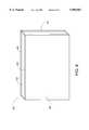
- FIG. 1is a perspective view of a wafer used to form spacers in accordance with the invention
- FIGS. 2-4are cross sectional views of a spacer formed from the wafer of FIG. 1;
- FIGS. 5a-5dare cross sectional views illustrating a method of forming a spacer in accordance with one embodiment of the invention.
- FIG. 6is a perspective view of spacers positioned between a faceplate structure and a backplate structure
- FIG. 7is a perspective view illustrating the connection of potential adjustment electrodes of a spacer to a power supply
- FIG. 8is a perspective view of a laminated wafer having an electrically insulating core and electrically resistive skins
- FIG. 9is a cross sectional view of a spacer formed from the laminated wafer of FIG. 8;
- FIG. 10is a perspective view of another wafer having an electrically insulating core and electrically resistive skins
- FIG. 11is a cross sectional view of a spacer formed from the wafer of FIG. 10;
- FIG. 12is a perspective view of yet another wafer having an electrically insulating core and electrically resistive skins.
- FIG. 13is a cross sectional view of a spacer formed from the wafer of FIG. 12.
- electrically conductive regionsare illustrated with thin angled lines
- electrically resistive regionsare illustrated with alternating thick and thin angled lines
- electrically insulating regionsare illustrated with thick angled lines.
- electrically insulatinggenerally applies to materials having a resistivity greater than 10 12 ohm-cm.
- electrically non-insulatingthus refers to materials having a resistivity below 10 12 ohm-cm. Electrically non-insulating materials are divided into (a) electrically conductive materials for which the resistivity is less than 1 ohm-cm and (b) electrically resistive materials for which the resistivity is in the range of 1 ohm-cm to 10 12 ohm-cm. These categories are determined at low electric fields.
- electrically conductive materialsare metals, metal-semiconductor compounds, and metal-semiconductor eutectics. Electrically conductive materials also include semiconductors doped (n-type or p-type) to a moderate or high level. Electrically resistive materials include intrinsic and lightly doped (n-type or p-type) semiconductors. Further examples of electrically resistive materials are cermet (ceramic with embedded metal particles) and other such metal-insulator composites. Electrically resistive materials also include conductive ceramics and filled glasses.
- a faceplate structuretypically includes an electrically insulating faceplate with a light emitting structure located on an interior surface of the faceplate.
- the backplate structuretypically includes an electrically insulating backplate with an electron emitting structure located on an interior surface of the backplate.
- Spacers in accordance with the inventioncan also be used in other flat panel displays such as plasma displays or vacuum fluorescent displays. Further, these spacers are not limited to use in displays, but can be used in other flat panel devices used for purposes such as optical signal processing, optical addressing in devices such as phased array radar devices, or in devices, such as copiers or printers, which scan an image to be reproduced on another medium. Additionally, the invention is applicable to flat panel devices having non-rectangular screen shapes, e.g., circular, and irregular screen shapes such as might be used in a vehicle dashboard or an aircraft control panel.
- a flat panel displayis a display in which the faceplate and backplate structures are substantially parallel, and the thickness of the display is small compared to the thickness of a conventional deflected-beam CRT display, the thickness of the display being measured in a direction substantially perpendicular to the faceplate and backplate structures.
- the thickness of a flat panel displayis less than 5 cm.
- the thickness of a flat panel displayis substantially less than 5 cm--e.g., 0.5-2.5 cm.
- Spacers of the inventioncan be used in flat panel displays such as those described in more detail in parent U.S. patent application Ser. No. 08/188,857, cited above; commonly owned, co-pending U.S. patent application Ser. No. 08/188,856 "Structure and Fabrication of Device with Raised Black Matrix for Use in Optical Displays Such as Flat-Panel Cathode-Ray Tubes," Curtin et al., filed Jan. 31, 1994, now U.S. Pat. No. 5,477,105; commonly owned, co-pending U.S. patent application Ser. No. 08/188,855, "Field Emitter with Focusing Ridges Situated to Sides of Gate,” Spindt et al., filed Jan.
- spacersthere are several methods of producing spacers in accordance with the invention. These methods include (1) manufacturing a spacer from a solid piece of uniform electrically resistive material such as a ceramic containing a transition metal oxide or a filled glass system in which the glass is made electrically resistive by the addition of a transition metal oxide and the fillers are chosen to provide the desired electron emission and thermal expansion match, (2) manufacturing a spacer by laminating electrically resistive skins on outside surfaces of an electrically insulating core, (3) manufacturing a spacer from an electrically insulating ceramic composition, wherein electrically resistive skins are formed at the outside surfaces of the spacer by reducing the outside surfaces of the ceramic composition, and (4) manufacturing a spacer by coating an electrically resistive material on an electrically insulating core.
- a spacerfrom a solid piece of uniform electrically resistive material such as a ceramic containing a transition metal oxide or a filled glass system in which the glass is made electrically resistive by the addition of a transition metal oxide and the fillers are chosen to
- the uniform resistive materialis an electrically resistive ceramic composition formed by combining a transition metal oxide such as iron oxide, titania, chromia, vanadium oxide or nickel oxide with an electrically insulating ceramic such as alumina. The combination of a transition metal oxide and the alumina results in a ceramic which has an electrical resistivity in the desired range of 10 5 to 10 10 ohm-cm.
- the replacement of as few as 4% of the aluminum cations in the aluminaresults in a resistivity in the desired range (i.e., 10 5 to 10 10 ohm-cm). Because of the small amount of titanium or iron required, the thermal coefficient of expansion (TCE) of the resulting composition is essentially the same as the TCE of alumina.
- a larger amount of chromiais combined with alumina to provide an electrical resistivity in the desired range.
- the effective inter-cation distance in the resulting lattice structuredecreases. This decreased inter-cation distance increases the overlap of electrons in the lattice structure, thereby forming a composition having the desired electrical resistivity.
- a ceramic including alumina and chromiacan contain up to 90% chromia by weight.
- chromiaadvantageously results in a ceramic having a low secondary electron emission.
- a ceramic composition of alumina and chromiacan have a secondary electron emission of less than two at 2 kV. This advantageously reduces the voltage deviation around the spacers.
- the TCE of the resulting ceramic compositioncan be controlled to be any value between the TCE of alumina (approximately 72) and the TCE of chromia (approximately 84).
- silicon dioxidesilicon dioxide
- Alumina and chromium sesquioxideare known to form a continuous range of solid solutions all having the corundum crystal structure. X-ray diffraction studies have shown that the crystal structure can be maintained as corundum even while accommodating up to 20% admixtures of silica.
- Other transition metal oxidessuch as oxides of iron or vanadium, can be used to create the electrically resistive ceramic composition.
- spacersare fabricated from a slurry created by mixing ceramic powders, organic binders and a solvent in a conventional ball mill.
- this slurryis a ceramic composition which includes 90% alumina and 10% titania (hereafter, the "90/10 alumina-titania composition").
- Table 1sets forth a formula for such a slurry.
- the slurryis a ceramic composition which includes 2% titanium, 34.3% alumina and 63.7% chromia (hereafter, the "2/34/64 composition").
- Table 2sets forth a formula for such a slurry.
- the ceramic formulaalso contains modifiers chosen to control grain size or aid sintering.
- modifierschosen to control grain size or aid sintering.
- Compoundssuch as silicon dioxide, magnesium oxide, and calcium oxide can be used as modifiers.
- the milled slurryis used to cast a tape having a thickness of 110-120 ⁇ m.
- this tapeis cut into large wafers which are 10 cm wide by 15 cm long.
- the wafersare then loaded onto a flat conventional setter and fired in air and/or a reducing atmosphere until the wafers exhibit the desired resistivity.
- the wafersare typically fired in a cold wall periodic kiln using a hydrogen atmosphere with a typical dew point of 24° C. If the organic components of the wafer are to be pyrolized (i.e., removed) in the same kiln, the dew point of the hydrogen atmosphere will be higher (approximately 50° C.) to facilitate removal of the organics without damaging the wafers. The dewpoint will be shifted from the higher dew point (50° C.) to the lower dewpoint (24° C.) after the organic components of the wafer are pyrolized. Pyrolysis is typically complete at a temperature of 600° C. Typically, the wafers are fired at a peak temperature of 1620° C. for 2.5 hours.
- the properties of the ceramic compositionare controlled by the detailed firing profile.
- the actual peak temperaturemay be between 1450° C. and 1750° C., and the firing profile may maintain this peak temperature from 1 to 16 hours.
- the wafersare then unloaded and inspected.
- the measured TCE of the resulting waferswas 71.6.
- the resulting wafershad a resistivity of approximately 10 8 ohm-cm.
- the 2/34/64 compositionresults in a resistivity of approximately 2 ⁇ 10 8 ohm-cm.
- Face metal stripesare formed on at least one face of the wafer. These face metal stripes will serve as electrodes on the face of the resulting spacer. Face metal stripes may be put down by any of a number of suitable techniques such as evaporation, sputtering photolithography, electroplating, screen printing, direct-pen writing, or by decomposition of an organometallic material with a laser beam.
- the following stepswould be appropriate.
- the waferis first masked so that the evaporated metal will fall only on the desired portions of the face of the wafer.
- the masked waferis placed in a vacuum chamber (not shown).
- the vacuum chambercontains an arrangement of containers which may be heated so that a metal (e.g., chromium, nickel or aluminum) placed within the containers is vaporized at low pressure.
- a metale.g., chromium, nickel or aluminum
- a metal stripeis formed on the surface of the wafer wherever there is an opening in the mask.
- the evaporation conditionsdepend upon the metal chosen to form the stripes and the condition of the wafer surface.
- the evaporation temperatureis typically in the vicinity of 1000° C., and the time to effect the evaporation is less than a minute.
- the vacuum evaporation apparatustypically has a port and other means by which the parts may be rapidly introduced into the chamber and the supply of metal replenished.
- the maskcan be made by standard photolithographic techniques. Such techniques allow fine metal stripes to be fabricated, especially during the fabrication of non planar spacer structures.
- photolithographic techniquesthe wafer is first coated with a commercial photoresist and the photoresist is cured. The cured resist is exposed by projection of the desired stripe pattern onto the surface. The surface of the wafer is exposed by washing away the unexposed photoresist. The wafer thus prepared is placed into the vacuum evaporator. Metal is evaporated onto the wafer surface in the manner previously described. The metallized wafer is removed from the chamber and the photoresist is chemically removed. During the photoresist removal, the metal lying on the photoresist is lifted off so that the metal electrode stripes are left on the face of the wafer.
- FIG. 1illustrates a wafer 100 having face metallization strips 101-105 located on outside surface 112 and face metallization strips 106-110 formed on outside surface 114.
- Wafer 100is greatly magnified for purposes of illustration.
- the face metallization strips on surface 112are aligned with the face metallization strips on surface 114.
- strip 103is situated substantially opposite strip 108.
- the center-to-center spacing between each of these face metallization stripsis typically 0.5 mm. As discussed below, this center-to-center spacing defines the spacer height.
- the face metal stripesmay also be applied by using materials similar to the thick film metallizations widely used to prepare hybrid circuits.
- These metallization materialsconsist of a mixture of a metal powder and powdered glass or other material that promotes adhesion of the metal to the ceramic.
- the metallization materialsare suspended in an organic binder that allows the combination to be deposited by any of a variety of common printing techniques. Stripes of this material may be applied through masks similar to those used for evaporation, by screen printing or by direct application of the stripes using a special pen. In all cases, the material must be fired to fuse the metal powder into a conductor and simultaneously bond the material to the ceramic.
- the oxidation state of the ceramic materials employed in the waferis crucial in determining the resistivity and charging behavior of the spacer.
- Maintaining this material in the proper oxidation statemay require that the firing of the electrode metallization be carried out in a neutral or reducing atmosphere.
- thick film metallization materialsare designed to fire at temperatures between 800° C. and 1000° C. While not all thick film metallizations are compatible with firing in atmospheres other than air, almost all manufacturers of these materials offer products specifically compounded for such firing.
- Wafer 100is subsequently cut along face metallization strips 101-110 to form spacers. Lines 121-123 indicate the locations of the cuts.
- This cutting stepcan be performed using a conventional saw having a diamond impregnated blade.
- FIG. 2illustrates a typical spacer 140 corresponding to the lowermost strip created after cutting along line 123 of wafer 100 (FIG. 1).
- Spacer 140has outside surfaces 112 and 114 and edge surfaces 126 and 128.
- Edge metallization stripscan be applied to the edge surfaces of each spacer.
- FIG. 3depicts spacer 140 after edge metallization strips 130 and 131 are applied to edge surfaces 126 and 128. Edge metallization strips 130 and 131 are applied using conventional techniques.
- Edge metallization strips 130 and 131Methods similar to those used for application of metal to the face of the wafer can be used to apply edge metallization strips 130 and 131. While there are differences in the fixturing required to orient the spacers so as to confine the metal to the edges, the process of applying the metallization material is only slightly altered. As a practical matter, in applying metal to the edges it is usual to gather the cut spacers into large blocks so that many may be processed at one time. Edge metallization has been placed on spacers by evaporating aluminum on the spacer edges and by screen printing silver, tungsten, or molybdenum-manganese on the spacer edges. Edge metallization has also been placed on spacers by combining silver or palladium with an organometallic material, screen coating the combination on the spacer edges, and thermally decomposing the combination at temperatures near 450° C.
- the resulting spacer structurecan be fired in accordance with conventional techniques. Final inspection is performed to complete the fabrication of spacer 140.
- FIG. 4depicts metal potential adjustment electrodes 161-162 formed on outside surface 112 of spacer 140.
- Potential adjustment electrodes 161-162are typically formed at the same time that face metallization strips 101-110 are formed. Potential adjustment electrodes 161-162 are approximately 0.025 mm wide.
- spacer 140has a height of approximately 1.27 mm, potential adjustment electrode 161 is located approximately 0.25 mm from electron emitting structure 172, and potential adjustment electrode 162 is located 0.76 mm from electron emitting structure 172.
- Edge metallization strip 130contacts light emitting structure 171 situated along faceplate 174.
- Edge metallization strip 131contacts electron emitting structure 172 situated along backplate 175.
- the voltages of light emitting structure 171, edge metallization strip 126, and face metallization strips 104 and 109are controlled by a power supply circuit 180, which is connected to at least two of the electrodes formed on outside surface 112.
- Power supply circuit 180is a conventional element which can take various forms. In FIG. 4, power supply circuit 180 is connected to face metallization electrodes 104 and 105, as well as potential correction electrodes 161 and 162.
- Power supply circuit 180provides a first voltage V1 to face metallization electrode 104, a second voltage V2 to potential correction electrode 162, a third voltage V3 to potential correction electrode 161 and a fourth voltage V4 to face metallization electrode 105, wherein V1>V2>V3>V4.
- Spacer 140is sufficiently thin that potential correction electrodes 161-162 control the voltage distribution at opposite surface 114. In alternative embodiments, potential correction electrodes are also included on surface 114.
- power supply circuit 180provides only a first voltage V1 to face metallization electrode 104 and a second voltage V4 to face metallization electrode 105.
- the voltages existing on potential correction electrodes 161-162are determined by the voltage divider circuit created by potential correction electrodes 161-162 and spacer 140. That is, the voltages on potential correction electrodes 161-162 are determined by the resistance of the portion of spacer 140 located between electrodes 104 and 162, the resistance of the portion of spacer 140 located between electrodes 162 and 161, and the resistance of the portion of spacer 140 located between electrodes 161 and 105.
- Potential adjustment electrodes 161-162control the voltage distribution along spacer 140. Stray electrons which strike outside surfaces 112 and 114 of spacer 140 travel to potential adjustment electrodes 161-162, thereby preventing charge build-up at the outside surfaces 112 and 114 of spacer 140.
- Power supply circuit 180is typically connected at the ends of spacer 140 which extend outside of the active regions of the faceplate and backplate structures 174 and 175.
- FIGS. 5a-5dillustrate a variation of Method (1).
- wafer 201is attached to glass substrate 200 with an adhesive 202.
- adhesive 202is wax-based bonding material.
- Face metallization layer 203is formed on wafer 201 by sputtering, evaporation or chemical deposition before wafer 201 is attached to glass substrate 200.
- Face metallization layer 203is patterned using conventional photolithographic methods to create face metal electrodes 205 (FIG. 5b). Face metal electrodes 205 are then coated with a protective film 206 (FIG. 5b). A layer of photoresist can be used to form protective film 206.
- Wafer 201is then sawed into strips 207 (FIG. 5c).
- strips 207have a length L of 1.27 mm and a height H of 0.064 mm.
- Edge metal electrodes 208(FIG. 5d).
- Protective film 206 and adhesive 202are dissolved, thereby separating strips 207 from glass substrate 200.
- Strips 207are then cleaned (e.g., ultrasonically).
- the green (unfired) ceramicis slit into strips.
- the organic elements of the unfired ceramic taperender the tape plastic and capable of being handled in similar fashion to conventional plastic sheet materials.
- the slittingcan be accomplished by feeding the unfired ceramic sheet through a conventional slitter similar to equipment used in the fabrication of paper and plastic products. These strips are then fired in specially designed fixtures to form the spacers. The fired strips can be metallized in a similar fashion to the wafer described above.
- the metallizationmay be a metal chosen to be compatible with the high firing temperature required to convert the green wafer to ceramic.
- This techniqueknown as cofiring, has been used to fabricate packages for mounting semiconductor integrated circuit devices.
- Metals used for cofiringinclude tungsten and molybdenum at high temperatures. Copper and silver can be cofired with low temperature glass ceramics. Wafers with stripes of metal applied in the green (unfired) state can be fabricated either into fired wafers which are subsequently cut into individual spacers, or cut into strips along the metallized stripes and fired as individual spacers.
- FIG. 6illustrates spacers 340 and 341 positioned between faceplate structure 350 and backplate structure 351 of a flat panel CRT display.
- Face metallization strips 330-333adjoin faceplate structure 350, and face metallization strips 334-337 adjoin backplate structure 351.
- Faceplate structure 350includes faceplate 302 and light emitting structure 306.
- Backplate structure 351includes backplate 303 and electron emitting structure 305.
- the internal surfaces of faceplate 302 and backplate 303are typically 0.1-2.5 mm apart.
- Faceplate 302is glass having, illustratively, a thickness of 1.0 mm.
- Backplate 303is glass, ceramic, or silicon having, illustratively, a thickness of 1.0 mm.
- the center-to-center spacing of spacers 340 and 341is, illustratively, 8 to 25 mm along dimension 316.
- Electron emitting structure 305includes electron-emissive elements (field emitters) 309, a patterned metallic emitter electrode (sometimes referred to as a base electrode) divided into a group of substantially identical straight emitter electrode lines 310, a metallic gate electrode divided into a group of substantially identical straight gate electrode lines 311, an electrically insulating layer 312 and focusing ridges 380.
- Other types of electron emitting structurescan be used with the spacers of the invention.
- Emitter electrode lines 310are situated on the interior surface of backplate 303 and extend parallel to one another at a uniform spacing.
- Insulating layer 312lies on emitter electrode lines 310 and on laterally adjoining portions of backplate 303.
- Gate electrode lines 311are situated on insulating layer 312 and extend parallel to one another (and perpendicular to emitter electrode lines 310) at a uniform spacing.
- Field emitters 309are distributed in an array above the interior surface of backplate 303.
- each group of field emitters 309is located above the interior surface of backplate 303 in part or all of the projected area where one of gate lines 311 crosses one of emitter lines 310.
- Spacers 340 and 341extend towards areas between field emitters 309 and also between emitter electrode lines 310.
- Each group of field emitters 309extends through an aperture (not shown) in insulating layer 312 to contact an underlying one of emitter electrode lines 310.
- the tops (or upper ends) of each group of field emitters 309are exposed through a corresponding opening (not shown) in an overlying one of gate electrode lines 311.
- Field emitters 309can have various shapes such as needle-like filaments or cones.
- Focusing ridges 380which extend above gate lines 311, are electrically isolated from gate lines 311. Focusing ridges 380 are described in more detail in U.S. patent application Ser. No. 08/188,855, cited above.
- Spacers 340 and 341(and face metallization strips 334-337) contact focusing ridges 380. In this case, face metallization strips 334-337 abut focusing ridges 380 and are held at the same potential as focusing ridges 380.
- An electrically conductive material(not shown) can also be located outside the active area of backplate structure 351 to provide an electrical connection between face metallization strips 334-337 and focusing ridges 380. This electrical connection prevents charge build-up near the ends of spacers 340 and 341 adjacent electron emitting structure 305.
- spacers 340 and 341include edge metallization strips (not shown).
- Light emitting structure 306is situated between faceplate 302 and spacers 340 and 341.
- Light emitting structure 306consists of a group of light emissive regions 313 (e.g., phosphor) that produce light when struck by electrons, a black matrix of substantially identical dark, non-reflective ridges 314 that do not produce light when struck by electrons, and a light reflective layer 315.
- Light emissive regions 313are divided into a plurality of substantially identical regions 313r, 313g and 313b that emit red (R), green (G) and blue (B) light, respectively.
- Light reflective layer 315 and, consequently, light emissive regions 313are maintained at a positive voltage of 1500-10,000 volts relative to the voltage of field emitters 309.
- one group of field emitters 309is suitably excited by appropriately adjusting the voltages of emitter electrode lines 310 and gate electrode lines 311, that group of field emitters 309 emits electrons which are accelerated towards a target light emissive region 313.
- FIG. 6illustrates trajectories 317 followed by one such group of electrons. Upon reaching the target light emissive region 313, the emitted electrons cause these phosphors to emit light 318.
- Some of the electronsinvariably strike parts of the light-emitting structure other than the target phosphors. As illustrated by trajectory 317a, some electrons strike the spacers.
- the black matrix formed by dark ridges 314compensates for off-target hits in the row direction to provide sharp contrast as well as high color purity.
- Light reflective layer 315typically aluminum, is situated on light emissive regions 313 and dark ridges 314 as shown in FIG. 6.
- the thickness of light reflective layer 315is sufficiently small that nearly all of the emitted electrons that strike layer 315 pass through layer 315 with little energy loss.
- the surface portions of layer 315 adjoining light emissive regions 313are quite smooth so that part of the light emitted by regions 313 is reflected by layer 315 through faceplate 302.
- Light reflective layer 315also acts as the anode for the display. Because light emissive regions 313 contact layer 315, the anode voltage is impressed on regions 313.
- Spacers 340 and 341contact light reflective layer 315 on the anode side of the display. Because dark ridges 314 extend further toward backplate 303 than light emissive regions 313, spacers 340 and 341 contact portions of layer 315 along the tops (or bottoms in the orientation shown in FIG. 6) of ridges 314. The extra height of ridges 314 prevents spacers 340 and 341 from contacting and damaging light emissive regions 313. Face metallization strips 330-333 abut layer 315 and are therefore electrically connected to layer 315.
- An electrically conductive materialcan also be located outside the active area of faceplate structure 350--i.e., around the outer edges of faceplate structure 350--to provide an electrical connection between face metallization strips 330-333, and layer 315.
- face metallization strips 330-333 and layer 315can extend to the outer edges of faceplate structure 350 to be electrically connected to an electrically conductive frit.
- the fritis a glass composite material which bonds the outer edges of faceplate structure 350 to the flat panel display.
- the fritis made electrically conductive by including metal particles in the glass composite material.
- face metallization strips 330-333 and layer 315cause face metallization strips 330-333 to be biased at the same high voltage as layer 315.
- stray electrons which strike the surface of spacers 340 and 341 near face metallization strips 330-333travel to face metallization strips 330-333. In this manner, charge build-up is prevented near the ends of spacers 340 and 341 adjacent light emitting structure 306.
- FIG. 7illustrates the connection of potential adjustment electrodes 701 and 702 of spacer 700 to power supply circuit 703 in accordance with the invention.
- Potential adjustment electrodes 701 and 702extend along spacer 700 outside of the active region of the flat panel display. Potential adjustment electrodes 701 and 702 then extend to one of the edge surfaces of spacer 700.
- Portions of electrically conductive frit material 715 and 716connect electrodes 701 and 702 to electrodes 711 and 712 on substrate 721 of the backplate structure 720.
- Electrodes 701 and 702connect to power supply circuit 703, thereby applying the desired voltages to potential adjustment electrodes 701 and 702. Frit portions 715 and 716 also help to support spacer 700.
- electrodes 701 and 702extend to the other edge surface of spacer 700 and are connected with frit material to corresponding electrodes on a faceplate structure (not shown).
- face metallization strips (not shown) on spacer 700are connected to electrodes formed on the faceplate or backplate structure in the manner previously described.
- FIG. 8depicts a laminated wafer 400 formed with an insulating ceramic core 401 and electrically resistive skins 402 and 403.
- insulating core 401is formed from an alumina ceramic tape having a thickness of 7.5-75 ⁇ m.
- the alumina core ceramicis prepared by first dispersing alumina powder in an organic material such that a homogenous distribution of the alumina powder in the organic material is achieved. The dispersion can be carried out in a ball mill, vibratory mill, planetary mill or other apparatus known to those skilled in the art.
- the dispersed powder organic mixis formed into tape by a process such as tape casting or roll compaction.
- tape castingthe organic slurry is carried under a doctor blade to level a thin film to a uniform height. By careful control of the solvents and other organic constituents, this film of slurry can be made to dry to a uniform film of a precise thickness.
- Another method of preparing tapeis to form the dispersed powder slurried in the organic mix into a tape by passing slurry through a pair of rollers. These rollers squeeze the tape to a uniform thickness. This is commonly called roll compaction.
- Feedstocks for roll compactionmay also be formed by spraying the ceramic powder dispersed in a binder and solvent mix into a special drying chamber. This process forms large particles of the powder and binders. By choice of proper ratios for the particular particle morphology of the powder this "spray dried" powder can be made free flowing. This free flowing powder forms a convenient feedstock for the roll compaction process.
- the 90/10 alumina-titania composition and the 2/34/64 composition discussed in connection with Method (1)are suitable for use as electrically resistive skins 402 and 403 in Method (2).
- Compositions that cannot be used to fabricate uniform electrically resistive spacers by reason of strength or uniformitycan be used to fabricate electrically resistive skins 402-403. As a result, the composition range is wider for resistive skins 402-403.
- the objectiveis to formulate a material with an electrical resistivity in the proper range and a low and controllable secondary electron emission.
- Solid solutions of chromium and aluminum oxidesare particularly useful. These compositions require firing in carefully controlled atmospheres. The conduction mechanism of such solid solutions is complex. Since the chromia and alumina form a solid solution, the separation between chromium cations is too great for easy transfer of the electrons between them. The charge carriers are therefore supplied by a small admixture of titanium dioxide. Titanium dioxide (titania) also aids the sintering of chromium sesquioxide by stabilizing the oxidation states. Subjecting titania to the reducing atmosphere needed to fire the chromia-alumina solid solution reduces the titania to a lower oxide state. This not only aids in the sintering of the body, but also provides the needed conductivity by partially reducing the oxidation state of the titania.
- the solubility of the titania in the crystals of chromia-alumina solid solutionis limited to approximately 2%.
- concentrations greater than 2%the majority of the titania is exuded to the grain boundaries of the material as the crystals grow during the sintering operation.
- concentration of the titaniais quite high in the more disordered material at the grain boundaries.
- the volume fraction of the material occupied by this less ordered materialis small compared to that of the grains of crystalline solid solution.
- the materialis rich in titania, the transfer of electrons between titanium cations of varying coordination is easy compared to that in the crystalline material that forms the bulk of the solid. Therefore the charge transport is mostly through the grain boundary materials in these compositions.
- the secondary electron generating properties of the titania-chromia-alumina solid solutionsare quite close to those of the pure chromium oxide which produces a desirable low charging current in spacers made of these materials, while the conductivity on the grain boundaries may be manipulated over a wide range by varying the admixture of titania.
- the sintering behavior of the titania-chromium-alumina materialsis complex. To make a suitable spacer the proper ratio of grain volume to grain boundary volume must be maintained while controlling not only the composition of the solid solution, but also the composition of the grain boundary.
- the firing conditions, particularly the peak temperature, the partial pressure of oxygen in the kiln atmosphere, the firing ramps, and the firing timesmust be appropriate to the particular composition being processed. Composition ranging from 10% chromium sesquioxide and 90% alumina to 90% chromium and 10% alumina have been made. These compositions have all been modified with 0.25% to 8% titanium dioxide.
- the kiln atmosphereshave ranged from 10 -20 atm oxygen partial pressure as water vapor in a hydrogen atmosphere to 3% oxygen as water vapor in a mixture of 20% hydrogen 80% nitrogen.
- the 2/34/64 compositionis cast into a tape having a thickness of approximately 0.05 mm.
- insulating coressuch as insulating core 401.
- the 2/34/64 composition tapeis cut into wafers to form electrically resistive skins, such as skins 402 and 403.
- Insulating core 401 and resistive skins 402 and 403have approximately the same length and width measurements.
- insulating core 401 and resistive skins 402-403can each be approximately 10 cm wide and 15 cm long.
- the spaceris formed of a laminate of resistive skins 402 and 403 on either side of insulating ceramic core 401.
- the layer thicknessesare chosen so that the completed laminate will have the desired spacer thickness.
- spacersare made by laminating 0.0127 mm thick resistive skins to a 0.3175 mm thick ceramic core.
- the layerscan be laminated by continuously feeding strips of the three unfired layers 401-403 through metal rollers adjusted to provide sufficient heat and pressure to fuse the green material. This provides a continuous and low cost method for fabricating the laminate. At a temperature of approximately 100° C., the unfired layers 401-403 easily fuse when passing through the rollers. As a result, laminated wafer 400 is formed.
- Method (2)--e.g., forming face and/or edge metallization strips--are similar to the steps previously described in connection with Method (1).
- the step of firing wafer 400 in a reducing atmosphereis performed such that laminated wafer 400 experiences a greater degree of reduction.
- Thisadvantageously reduces the electrical resistivity of resistive skins 402 and 403 without significantly decreasing the bulk resistivity of the spacer.
- the desired electrical resistivity of resistive skins 402 and 403is 10 5 -10 10 ohm-cm.
- FIG. 9illustrates a spacer 404 formed by Method (2).
- Spacer 404includes portions of insulating core 401 and electrically resistive skins 402 and 403.
- Spacer 404includes face metallization strips 405 and 406 on outside surface 407 of resistive skin 402, and face metallization strips 408 and 409 on outside surface 410 of resistive skin 403.
- Spacer 404also includes edge metallization strip 412 formed on edge surface 414 and edge metallization strip 416 formed on edge surface 418.
- Spacer 404can also be fabricated with only face metallization strips 405-406 and 408-409 or only edge metallization strips 412 and 416.
- the total thickness of the laminated spacer formed by Method (2)is approximately the same as the thickness of the solid spacer formed by Method (1).
- Resistive skins 402 and 403can be cast at a minimum thickness of 70-80 ⁇ m.
- Laminated spacer 404 formed by Method (2)advantageously exhibits a high bulk resistivity because of the insulating characteristics of core 401.
- the strength of laminated spacer 404is approximately equal to the strength of the material used to fabricate insulating core 401 (e.g., alumina). Furthermore, the steps set forth in connection with Method (2) make it relatively easy to control the sheet resistance of skins 402 and 403.
- defects such as pinholesare not as important as they are for spacers of solid construction.
- a small pin holedoes not adversely affect the operation of spacer 404 for two reasons.
- One reasonis that a hole which is smaller in diameter than the thickness of skins 402 and 403 still effectively shields insulating core 401 from the electrons which are transmitted between the faceplate and backplate structures.
- the other reasonis that the strength and other performance factors of spacer 404 are largely unaffected by small defects in skins 402 and 403 since such defects terminate at core 401 and therefore can not propagate through core 401 to cause failure of spacer 404.
- laminated waferssuch as laminated wafer 400 are fabricated with skins made of other ceramic compositions which include ceramics containing transition metal oxides.
- ceramics containing transition metal oxidesThere are many compositions which are suitable for such spacers.
- transition metal oxide compositions previously describedthere are compositions containing copper (e.g., copper oxide), families of chalcoginides, and semiconductors with resistivities in the proper range.
- the electrically insulating ceramic core of the spacercan be formed from a ceramic composition, such as alumina containing a transition metal oxide, wherein the transition metal oxide is present in the higher oxide states. Electrically resistive skins are formed at the outside surfaces of the spacer by chemically reducing the outside surfaces of the spacer. By reducing the outside surfaces of the spacer, the coordination of the transition metal ions at these outside surfaces is altered, thereby causing the transition metal oxide to become electrically resistive at the outside surfaces of the spacer.
- the spacer coreremains electrically insulating.
- the reducing stepcan be performed in a number of different ways, including firing the spacer in a reducing atmosphere, or exposing the spacer to a laser beam, charged particles or photon irradiation.
- Spacers fabricated in accordance with Method (3)are formed from a ceramic composition which is formulated such that the electrical resistivity of the composition can be altered by selective reduction.
- the ceramic compositionis selected such that the resistivity of the composition is a function of the oxidation state of at least one component of the composition.
- the ceramic compositionis also selected such that the crystal structure of the composition allows the electrical resistivity of the composition to be altered by selective reduction of the surface of the composition.
- Compositions which exhibit these propertiesinclude glasses containing transition metal oxides, non-centrosymmetric titanates such as barium titanate, lead titanate and bismuth titanate. Mixtures of these compositions can also be used. Commercial materials, such as iron and chromium containing glasses (typically used as glazes for high voltage insulator strings), can also be used.
- the resistivityis determined by the ratio of the transition metal cations in one coordination to the transition metal cations in another coordination.
- the ratio of Ti 3+ to Ti 4+ cationsdetermines the resistivity of the composition.
- vanadium cationsare the charge carriers
- the ratio of V 4+ to V 5+ cationsdetermines the resistivity.
- the superscripted numbersindicate the number of nearest neighbor oxygen anions.
- transition metal cationbe bound in the composition such that the oxidation state of the cation can be altered by a displacive (rather than reconstructive) transformation of the crystal lattice of the composition.
- the displacive transformationis effected at temperatures well below the melting point of the material, but substantially above the temperature the spacer will experience during normal use in a flat panel display. Consequently, the electrical properties of the composition remain stable during use.
- One method of formulating a suitable ceramic compositionis to dissolve a transition metal in a silicate glass.
- the transition metal cationsprovide the charge carriers to provide electrical conductivity.
- the number of charge carriers present in the materialdepends on the ratio of the cations in the two relevant coordinations (e.g., Ti 3+ and Ti 4+ in the case of titanium).
- the number of cations in each coordinationis a function of the total oxidation state of the composition. If this oxidation state is altered, the conductivity is also altered.
- a glass or glass ceramic containing transition metal ionsmay be altered by oxidation or reduction at low temperatures if the crystal structure permits displacive transformation of the cation coordination.
- a transition metal oxide glasscan serve as the spacer, or the glass may be filled with other ceramic components to produce a material with a TCE and secondary electron emission tailored to particular values.
- transition metal oxideis dispersed in a very stable crystal, it is very difficult to alter the coordination of the cations. To substantially reduce the electrical resistivity of such a crystal, high temperature reconstructive transformations must be induced.
- a chromia-alumina solid solutionprovides an example of a stable crystal which must undergo reconstructive transformation to reduce the resistivity of the solid solution.
- the spaceris formed and fired in a manner similar to that previously described in connection with Method (1).
- the firing atmosphereis dictated by the selection of the oxide system which provides the conduction. For example, if titanium or iron is selected as the active cation, then an initial firing step is carried out in air. This air firing would place most of the titanium or iron cations in higher coordination sites (e.g., Ti 4+ ). Thus, the ratio of cations in the lower coordination sites (e.g., Ti 3+ ) to those in the higher coordination sites (e.g., Ti 4+ ) is low. Consequently, the resulting composition is electrically insulating.
- a resistive layeris formed on the outer surface of the composition by a second firing in a reducing atmosphere.
- This second firingcreates vacancies in the anion lattice surrounding some of the titanium or iron cations.
- the ratio of Ti 3+ to Ti 4+ cations(assuming titania is used) is raised and the composition becomes more conductive at the outer surface.
- the depth of these electrically resistive skinscan be controlled by choosing a proper combination of firing time and temperature. For example, resistive skins have been formed on air fired lead barium titanate compositions by exposure to 10% hydrogen, 90% nitrogen atmospheres for eight hours at 950° C. After the resistive skin has been formed on a wafer, the wafer can then be metallized and cut to form the spacers.
- the thickness and resistivity of the resistive skinscan be selected to reduce the power dissipated in the spacer, or allow the use of a material with a lower surface resistivity without incurring a penalty in the power consumed.
- the electrically resistive skinsare typically processed to produce a resistivity in the range of 10 6 to 10 9 ohm-cm.
- FIG. 10is a perspective view of a wafer 500 formed in accordance with Method (3).
- wafer 500has a thickness of approximately 100 ⁇ m.
- FIG. 11depicts a spacer 510 formed from wafer 500.
- Electrically resistive skins 502 and 503provide a gradual transition from a relatively low surface resistivity at outside surfaces 504 and 505 to a relatively high bulk resistivity at core 501.
- Face metallization strips 516 and 517are formed on outside surface 504, and face metallization strips 519 and 520 are formed on outside surface 505 of spacer 510.
- Edge metallization strips 524 and 525are formed on edge surfaces 526 and 527, respectively.
- Metallization strips 516-517, 519-520 and 524-525are formed in a manner similar to that previously described in connection with Method (1).
- wafer 500is slit into strips before the initial firing step.
- the transition metal oxide at all of the exterior surfacesincluding outside surfaces 504 and 505 and edge surfaces 526 and 527) becomes electrically resistive.
- B 2 O 3is included in the ceramic composition to lower the firing temperature and the resistivity without raising the secondary electron emission of the resulting spacer.
- a spacer fabricated in accordance with Method (3)advantageously has a high bulk resistivity and a low secondary emission coefficient. Such a spacer therefore results in reduced power loss and reduced voltage variations proximate the spacer during operation of the flat panel display.
- a wafer 600is formed by placing an electrically resistive coating onto a solid electrically insulating core (or wafer), and firing the resulting structure.
- FIG. 12depicts a wafer 600 formed in accordance with Method (4).
- Solid, electrically insulating core 601can be fabricated by casting or compacting 100% alumina ceramic into a tape having a thickness of 100 ⁇ m. The tape is cut into wafers (or strips) and fired at a temperature between 1500 and 1700° C. for approximately two hours.
- Electrically resistive coatings 602 and 603are applied to core 601 while core 601 is in a large wafer format. Core 601 and resistive coatings 602-602 are fired and then cut into strips to make spacers.
- Electrically resistive coatings 602 and 603are applied to core 601 using any method which can be used to apply paint or dye to a surface. These methods include screen printing, spraying, roll coating, doctor blading or applying a decal. Some of these methods are described below.
- the resistive materialis applied as a paste or ink which is formed by placing the resistive material in an organic suspension.
- the suspensionis forced through a mesh (usually stainless steel) in a manner very similar to that used to make decorative patterns on T-shirts or to print posters.
- the pasteis placed on top of the screen and a squeegee blade rubs a thin coat of paste through the screen onto the underlying core 601.
- a precisely controlled layer of the pasteis transferred to core 601.
- the resistive materialmay be dispersed as a thinner liquid and sprayed onto the surface of core 601. This process is similar to paint spraying.
- a thin layer of the resistive material in an organic suspensionis squeezed onto the surface of core 601 by passing the substrate under specially grooved rubber rollers.
- Precise coating thicknessescan also be applied by doctor blading.
- doctor bladinga pool of the resistive material in an organic suspension is trapped behind a blade positioned above core 601. By moving core 601 relative to the blade and the pool at a constant speed, a constant and controlled thickness of the material is dragged under the blade and onto the surface.
- the resistive materialcan also be dispersed in an organic material to form a tape using a method similar to the tape preparation methods previously described. This tape is cut to match the size of core 601, and pressed onto core 601.
- the plastic component of core 601is chosen to provide adhesion or a separate adhesive layer may be applied.
- Acceptable resistive materialsinclude, but are not limited to, the various electrically resistive ceramic compositions previously described.
- Core 601 and electrically resistive coatings 602 and 603are fired in accordance with the parameters previously set forth in connection with Method (1).
- the fired wafer 600is processed in the same manner as previously described in connection with Method (1).
- FIG. 13shows a spacer 610 formed from wafer 600.
- Spacer 610includes electrically insulating core 601 and electrically resistive coatings 602 and 603.
- Face metallization strips 615 and 616are formed on outside surface 617 of spacer 610, and face metallization strips 619 and 620 are formed on outside surface 621 of spacer 610.
- Edge metallization strips 624 and 625are formed on edge surfaces 626 and 627 of spacer 610.
- the resistive coatings 602 and 603are applied to insulating core 601 before the insulating core 601 is fired.
- acceptable resistive coatingsinclude, but are not limited to, the previously described combinations of alumina and transition metal oxides.
- the electrically resistive coatingsare typically applied by screen printing, spray painting, roll coating, doctor blading or applying a decal.
- This variation of Method (4)may require an additional reduction step if the diffusion of the resistive coatings 602-603 into core 601 produces layers which are lower in conductivity than desired. In general, the greater the extent of the diffusion, the lower the conductivity of coatings 602-603.
- the reduction stepprovides a thin conductive layer on the surface of coatings 602-603 in a manner similar to that previously described in connection with Method (3).
- resistive coatings 602 and 603are formed from conductive glazes developed for suppressing electrical breakdown in high voltage insulators. These glazes exhibit the desired electrical resistivity and can be processed at reasonably low temperatures. Transition metals, such as iron, chromium, or titanium, can also be dissolved in these glazes to form acceptable resistive coatings. There are a number of commercial compositions used for this purpose. Most contain dissolved iron, titanium and/or chromium in the form of oxides.
- Methods (1) through (4)are described in connection with alumina ceramic cores, it is possible to use other ceramic compositions, such as mullites, cordiorites, barium borosilicates, iron silicates, filled glasses, and zero shrink tolerance (ZST) materials.
- ZST materialsobtain their unique properties by balancing the behavior of glass and ceramic filler components.
- a transition metal oxidecan be admixed into the glass component without drastically altering the properties of the ZST material. Because the glass forms a continuous matrix throughout the structure of the ZST material, making the glass phase a controlled conductor is sufficient to control the electrical resistivity of the spacer.
- each of these spacersmay alternatively include only edge metallization strips or only face metallization strips. Moreover, each of these spacers may also include potential adjustment electrodes as described in connection with Method (1).
Landscapes
- Engineering & Computer Science (AREA)
- Manufacturing & Machinery (AREA)
- Cathode-Ray Tubes And Fluorescent Screens For Display (AREA)
- Vessels, Lead-In Wires, Accessory Apparatuses For Cathode-Ray Tubes (AREA)
- Manufacture Of Electron Tubes, Discharge Lamp Vessels, Lead-In Wires, And The Like (AREA)
- Gas-Filled Discharge Tubes (AREA)
Abstract
Description
TABLE 1 ______________________________________ Alumina powder 292 grams Titania powder 32 grams Butvar B76 34 grams Santicizer 150 10 grams Kellox Z3 Menahden oil 0.65gram Ethanol 105 grams Toluene 127 grams ______________________________________
TABLE 2 ______________________________________ Alumina powder 111.1 grams Chromia powder 206.4 grams Titania powder 6.48 grams Butvar B76 34 grams Santicizer 150 10 grams Kellox Z3 Menahden oil 0.65gram Ethanol 105 grams Toluene 127 grams ______________________________________
Claims (46)
Priority Applications (1)
| Application Number | Priority Date | Filing Date | Title |
|---|---|---|---|
| US08/962,088US5985067A (en) | 1992-04-10 | 1997-10-31 | Formation of spacers suitable for use in flat panel displays |
Applications Claiming Priority (6)
| Application Number | Priority Date | Filing Date | Title |
|---|---|---|---|
| US07/867,044US5424605A (en) | 1992-04-10 | 1992-04-10 | Self supporting flat video display |
| US08/012,542US5589731A (en) | 1992-04-10 | 1993-02-01 | Internal support structure for flat panel device |
| US18885794A | 1994-01-31 | 1994-01-31 | |
| US08/414,408US5675212A (en) | 1992-04-10 | 1995-03-31 | Spacer structures for use in flat panel displays and methods for forming same |
| US08/739,773US5865930A (en) | 1992-04-10 | 1996-10-30 | Formations of spacers suitable for use in flat panel displays |
| US08/962,088US5985067A (en) | 1992-04-10 | 1997-10-31 | Formation of spacers suitable for use in flat panel displays |
Related Parent Applications (1)
| Application Number | Title | Priority Date | Filing Date |
|---|---|---|---|
| US08/739,773DivisionUS5865930A (en) | 1982-04-10 | 1996-10-30 | Formations of spacers suitable for use in flat panel displays |
Publications (1)
| Publication Number | Publication Date |
|---|---|
| US5985067Atrue US5985067A (en) | 1999-11-16 |
Family
ID=23641326
Family Applications (6)
| Application Number | Title | Priority Date | Filing Date |
|---|---|---|---|
| US08/414,408Expired - LifetimeUS5675212A (en) | 1982-04-10 | 1995-03-31 | Spacer structures for use in flat panel displays and methods for forming same |
| US08/739,773Expired - LifetimeUS5865930A (en) | 1982-04-10 | 1996-10-30 | Formations of spacers suitable for use in flat panel displays |
| US08/893,407Expired - LifetimeUS5916396A (en) | 1982-04-10 | 1997-07-11 | Formation of spacers suitable for use in flat panel displays |
| US08/962,088Expired - LifetimeUS5985067A (en) | 1992-04-10 | 1997-10-31 | Formation of spacers suitable for use in flat panel displays |
| US09/259,391Expired - Fee RelatedUS6157123A (en) | 1982-04-10 | 1999-02-26 | Flat panel display typically having transition metal oxide in ceramic core or/and resistive skin of spacer |
| US09/617,591Expired - Fee RelatedUS6489718B1 (en) | 1982-04-10 | 2000-07-18 | Spacer suitable for use in flat panel display |
Family Applications Before (3)
| Application Number | Title | Priority Date | Filing Date |
|---|---|---|---|
| US08/414,408Expired - LifetimeUS5675212A (en) | 1982-04-10 | 1995-03-31 | Spacer structures for use in flat panel displays and methods for forming same |
| US08/739,773Expired - LifetimeUS5865930A (en) | 1982-04-10 | 1996-10-30 | Formations of spacers suitable for use in flat panel displays |
| US08/893,407Expired - LifetimeUS5916396A (en) | 1982-04-10 | 1997-07-11 | Formation of spacers suitable for use in flat panel displays |
Family Applications After (2)
| Application Number | Title | Priority Date | Filing Date |
|---|---|---|---|
| US09/259,391Expired - Fee RelatedUS6157123A (en) | 1982-04-10 | 1999-02-26 | Flat panel display typically having transition metal oxide in ceramic core or/and resistive skin of spacer |
| US09/617,591Expired - Fee RelatedUS6489718B1 (en) | 1982-04-10 | 2000-07-18 | Spacer suitable for use in flat panel display |
Country Status (7)
| Country | Link |
|---|---|
| US (6) | US5675212A (en) |
| EP (1) | EP0818051B1 (en) |
| JP (1) | JP3340440B2 (en) |
| KR (1) | KR100352534B1 (en) |
| AU (1) | AU5364996A (en) |
| DE (1) | DE69633054T2 (en) |
| WO (1) | WO1996030926A1 (en) |
Cited By (13)
| Publication number | Priority date | Publication date | Assignee | Title |
|---|---|---|---|---|
| WO2000034975A1 (en)* | 1998-12-11 | 2000-06-15 | Candescent Technologies Corporation | Flat panel display, porous spacer structure and methods |
| US20020105408A1 (en)* | 1998-09-08 | 2002-08-08 | Masaki Aoki | Resistor for cathode ray tube |
| US6617772B1 (en) | 1998-12-11 | 2003-09-09 | Candescent Technologies Corporation | Flat-panel display having spacer with rough face for inhibiting secondary electron escape |
| US20030178216A1 (en)* | 2002-02-06 | 2003-09-25 | Ngk Insulators, Ltd. | Structure of retaining cut-processed components, method of fabricating cut-processed components, tray for housing cut-processed components, and method of cleaning cut-processed components |
| US6677706B1 (en)* | 1997-03-21 | 2004-01-13 | Canon Kabushiki Kaisha | Electron emission apparatus comprising electron-emitting devices, image-forming apparatus and voltage application apparatus for applying voltage between electrodes |
| US20040121258A1 (en)* | 2002-12-18 | 2004-06-24 | Xerox Corporation | Method of casting photoresist onto substrates |
| US6774554B1 (en)* | 1999-09-21 | 2004-08-10 | Matsushita Electric Industrial Co., Ltd. | Cathode ray tube |
| KR100486499B1 (en)* | 2002-09-28 | 2005-04-29 | 엘지전자 주식회사 | Beam distortion preventing method for field emisssion display |
| US20090058257A1 (en)* | 2007-08-28 | 2009-03-05 | Motorola, Inc. | Actively controlled distributed backlight for a liquid crystal display |
| US20090102350A1 (en)* | 2007-10-18 | 2009-04-23 | Motorola, Inc. | Field emitter spacer charge detrapping through photon excitation |
| US20100107435A1 (en)* | 2008-10-31 | 2010-05-06 | Jacob George | Methods and Apparatus for Drying Ceramic Green Bodies with Microwaves |
| US20110043698A1 (en)* | 2009-08-24 | 2011-02-24 | Canon Kabushiki Kaisha | Display panel, display and image display apparatus |
| US20130337241A1 (en)* | 2011-05-13 | 2013-12-19 | Byd Company Limited | Method for selectively metallizing surface of ceramic substrate, ceramic product and use of ceramic product |
Families Citing this family (103)
| Publication number | Priority date | Publication date | Assignee | Title |
|---|---|---|---|---|
| US5675212A (en) | 1992-04-10 | 1997-10-07 | Candescent Technologies Corporation | Spacer structures for use in flat panel displays and methods for forming same |
| CA2073923C (en) | 1991-07-17 | 2000-07-11 | Hidetoshi Suzuki | Image-forming device |
| JPH09167583A (en)* | 1995-12-15 | 1997-06-24 | Futaba Corp | Display device |
| JPH11510647A (en)* | 1996-05-28 | 1999-09-14 | フィリップス エレクトロニクス ネムローゼ フェンノートシャップ | Organic electroluminescent device |
| US5859502A (en)* | 1996-07-17 | 1999-01-12 | Candescent Technologies Corporation | Spacer locator design for three-dimensional focusing structures in a flat panel display |
| US6049165A (en) | 1996-07-17 | 2000-04-11 | Candescent Technologies Corporation | Structure and fabrication of flat panel display with specially arranged spacer |
| US5898266A (en)* | 1996-07-18 | 1999-04-27 | Candescent Technologies Corporation | Method for displaying frame of pixel information on flat panel display |
| US6008573A (en)* | 1996-10-04 | 1999-12-28 | International Business Machines Corporation | Display devices |
| US6278066B1 (en) | 1996-12-20 | 2001-08-21 | Candescent Technologies Corporation | Self-standing spacer wall structures |
| JPH10326579A (en) | 1997-03-28 | 1998-12-08 | Canon Inc | Image forming apparatus and manufacturing method thereof |
| JP3703287B2 (en) | 1997-03-31 | 2005-10-05 | キヤノン株式会社 | Image forming apparatus |
| JP3195290B2 (en)* | 1997-03-31 | 2001-08-06 | キヤノン株式会社 | Image forming device |
| US5831383A (en)* | 1997-05-12 | 1998-11-03 | Motorola Inc. | Spacer pads for field emission device |
| US5920151A (en)* | 1997-05-30 | 1999-07-06 | Candescent Technologies Corporation | Structure and fabrication of electron-emitting device having focus coating contacted through underlying access conductor |
| US6200181B1 (en)* | 1997-07-01 | 2001-03-13 | Candescent Technologies Corporation | Thermally conductive spacer materials and spacer attachment methods for thin cathode ray tube |
| US6169358B1 (en)* | 1997-07-11 | 2001-01-02 | Emagin Corporation | Method and apparatus for flashover control, including a high voltage spacer for parallel plate electron beam array devices and method of making thereof |
| US6218777B1 (en)* | 1997-07-11 | 2001-04-17 | Emagin Corporation | Field emission display spacer with guard electrode |
| US6208072B1 (en) | 1997-08-28 | 2001-03-27 | Matsushita Electronics Corporation | Image display apparatus with focusing and deflecting electrodes |
| JP3457162B2 (en) | 1997-09-19 | 2003-10-14 | 松下電器産業株式会社 | Image display device |
| JP3428397B2 (en)* | 1997-10-14 | 2003-07-22 | 松下電器産業株式会社 | Organic electroluminescent device and method of manufacturing the same |
| TW392186B (en)* | 1997-12-01 | 2000-06-01 | Hitachi Ltd | Plasma display panel and image display using the same |
| US6630782B1 (en) | 1997-12-01 | 2003-10-07 | Matsushita Electric Industrial Co., Ltd. | Image display apparatus having electrodes comprised of a frame and wires |
| US6236381B1 (en) | 1997-12-01 | 2001-05-22 | Matsushita Electronics Corporation | Image display apparatus |
| US6168490B1 (en)* | 1997-12-19 | 2001-01-02 | Sarnoff Corporation | Back panel for a plasma display device |
| US6278235B1 (en) | 1997-12-22 | 2001-08-21 | Matsushita Electronics Corporation | Flat-type display apparatus with front case to which grid frame with extended electrodes fixed thereto is attached |
| EP0926698A3 (en)* | 1997-12-25 | 2001-10-17 | Pioneer Electronic Corporation | Electron emitting device based flat panel display apparatus |
| JPH11191383A (en) | 1997-12-26 | 1999-07-13 | Matsushita Electron Corp | Flat image display device |
| WO1999034390A1 (en)* | 1997-12-29 | 1999-07-08 | Motorola Inc. | Field emission device having high capacitance spacer |
| US5990613A (en)* | 1998-01-20 | 1999-11-23 | Motorola, Inc. | Field emission device having a non-coated spacer |
| US6168737B1 (en) | 1998-02-23 | 2001-01-02 | The Regents Of The University Of California | Method of casting patterned dielectric structures |
| US6153075A (en) | 1998-02-26 | 2000-11-28 | Micron Technology, Inc. | Methods using electrophoretically deposited patternable material |
| US5990614A (en)* | 1998-02-27 | 1999-11-23 | Candescent Technologies Corporation | Flat-panel display having temperature-difference accommodating spacer system |
| US6107731A (en)* | 1998-03-31 | 2000-08-22 | Candescent Technologies Corporation | Structure and fabrication of flat-panel display having spacer with laterally segmented face electrode |
| JPH11312480A (en) | 1998-04-28 | 1999-11-09 | Matsushita Electron Corp | Flat panel image display device |
| US6506087B1 (en)* | 1998-05-01 | 2003-01-14 | Canon Kabushiki Kaisha | Method and manufacturing an image forming apparatus having improved spacers |
| US6113708A (en)* | 1998-05-26 | 2000-09-05 | Candescent Technologies Corporation | Cleaning of flat-panel display |
| US6051937A (en)* | 1998-05-29 | 2000-04-18 | Candescent Technologies Corporation | Voltage ratio regulator circuit for a spacer electrode of a flat panel display screen |
| KR100396367B1 (en)* | 1998-06-18 | 2003-09-02 | 후다바 덴시 고교 가부시키가이샤 | Aluminum paste for fluorescent display device, fluorescent display device using aluminum paste and method for manufacturing same |
| JP3073491B2 (en)* | 1998-06-24 | 2000-08-07 | キヤノン株式会社 | Electron beam apparatus, image forming apparatus using the same, and method of manufacturing members used in the electron beam apparatus |
| JP3099003B2 (en) | 1998-07-02 | 2000-10-16 | キヤノン株式会社 | Image forming device |
| US6414428B1 (en) | 1998-07-07 | 2002-07-02 | Candescent Technologies Corporation | Flat-panel display with intensity control to reduce light-centroid shifting |
| CN1309813A (en)* | 1998-07-27 | 2001-08-22 | 摩托罗拉公司 | Field emission display having adhesively attached spacers and attachment process |
| JP3689598B2 (en)* | 1998-09-21 | 2005-08-31 | キヤノン株式会社 | Spacer manufacturing method and image forming apparatus manufacturing method using the spacer |
| EP0993016B1 (en)* | 1998-09-29 | 2006-11-08 | Matsushita Electric Industrial Co., Ltd. | Plasma display panel and method of disassembling the same |
| JP4115050B2 (en)* | 1998-10-07 | 2008-07-09 | キヤノン株式会社 | Electron beam apparatus and spacer manufacturing method |
| US6392334B1 (en) | 1998-10-13 | 2002-05-21 | Micron Technology, Inc. | Flat panel display including capacitor for alignment of baseplate and faceplate |
| US6433473B1 (en)* | 1998-10-29 | 2002-08-13 | Candescent Intellectual Property Services, Inc. | Row electrode anodization |
| KR100304906B1 (en)* | 1999-02-24 | 2001-09-26 | 구자홍 | Plasma Display Panel having Floating electrode |
| US6861798B1 (en) | 1999-02-26 | 2005-03-01 | Candescent Technologies Corporation | Tailored spacer wall coatings for reduced secondary electron emission |
| US6236157B1 (en)* | 1999-02-26 | 2001-05-22 | Candescent Technologies Corporation | Tailored spacer structure coating |
| US6653769B1 (en)* | 1999-06-17 | 2003-11-25 | Kyocera Corporation | Spacers used for picture display devices and a method of producing the same |
| US6366009B1 (en)* | 1999-08-02 | 2002-04-02 | Motorola, Inc. | Method for fabricating a field emission display having a spacer with a passivation layer |
| US6215242B1 (en)* | 1999-09-15 | 2001-04-10 | St. Clair Intellectual Property Consultants, Inc. | Field emission display device having a photon-generated electron emitter |
| KR100316780B1 (en)* | 2000-02-15 | 2001-12-12 | 김순택 | Triode carbon nanotube field emission display using barrier rib structure and manufacturing method thereof |
| FR2806075B1 (en) | 2000-03-07 | 2002-09-20 | Saint Gobain Vitrage | GLASS SPACER |
| US6441559B1 (en) | 2000-04-28 | 2002-08-27 | Motorola, Inc. | Field emission display having an invisible spacer and method |
| US6551720B2 (en) | 2000-05-02 | 2003-04-22 | Sarnoff Corporation | Materials to fabricate a high resolution plasma display back panel |
| US6432593B1 (en) | 2000-05-31 | 2002-08-13 | Candescent Technologies Corporation | Gripping multi-level structure |
| US6733354B1 (en)* | 2000-08-31 | 2004-05-11 | Micron Technology, Inc. | Spacers for field emission displays |
| JP2002157959A (en) | 2000-09-08 | 2002-05-31 | Canon Inc | Method of manufacturing spacer and method of manufacturing image forming apparatus using this spacer |
| US6762566B1 (en) | 2000-10-27 | 2004-07-13 | Science Applications International Corporation | Micro-component for use in a light-emitting panel |
| US6545422B1 (en) | 2000-10-27 | 2003-04-08 | Science Applications International Corporation | Socket for use with a micro-component in a light-emitting panel |
| US7288014B1 (en) | 2000-10-27 | 2007-10-30 | Science Applications International Corporation | Design, fabrication, testing, and conditioning of micro-components for use in a light-emitting panel |
| US6570335B1 (en) | 2000-10-27 | 2003-05-27 | Science Applications International Corporation | Method and system for energizing a micro-component in a light-emitting panel |
| US6612889B1 (en) | 2000-10-27 | 2003-09-02 | Science Applications International Corporation | Method for making a light-emitting panel |
| US6796867B2 (en) | 2000-10-27 | 2004-09-28 | Science Applications International Corporation | Use of printing and other technology for micro-component placement |
| US6801001B2 (en) | 2000-10-27 | 2004-10-05 | Science Applications International Corporation | Method and apparatus for addressing micro-components in a plasma display panel |
| US6620012B1 (en) | 2000-10-27 | 2003-09-16 | Science Applications International Corporation | Method for testing a light-emitting panel and the components therein |
| US6935913B2 (en) | 2000-10-27 | 2005-08-30 | Science Applications International Corporation | Method for on-line testing of a light emitting panel |
| US6764367B2 (en) | 2000-10-27 | 2004-07-20 | Science Applications International Corporation | Liquid manufacturing processes for panel layer fabrication |
| US6822626B2 (en) | 2000-10-27 | 2004-11-23 | Science Applications International Corporation | Design, fabrication, testing, and conditioning of micro-components for use in a light-emitting panel |
| US6630786B2 (en)* | 2001-03-30 | 2003-10-07 | Candescent Technologies Corporation | Light-emitting device having light-reflective layer formed with, or/and adjacent to, material that enhances device performance |
| US6587351B2 (en)* | 2001-04-05 | 2003-07-01 | Cooper Technologies | Surface mount standoff for printed circuit board assembly |
| US6742257B1 (en)* | 2001-10-02 | 2004-06-01 | Candescent Technologies Corporation | Method of forming powder metal phosphor matrix and gripper structures in wall support |
| CN100338534C (en)* | 2002-01-24 | 2007-09-19 | 日东工业株式会社 | Color powder feeding roller |
| US6995502B2 (en)* | 2002-02-04 | 2006-02-07 | Innosys, Inc. | Solid state vacuum devices and method for making the same |
| FR2838118B1 (en)* | 2002-04-08 | 2004-09-10 | Saint Gobain | SPACERS HAVING ELECTRONIC CONDUCTIVITY, MANUFACTURING METHOD AND APPLICATIONS IN PARTICULAR FOR VISUALIZATION SCREENS |
| KR100463190B1 (en)* | 2002-06-12 | 2004-12-23 | 삼성에스디아이 주식회사 | Spacer structure with metal mesh and flat panel display device having the same |
| JP3724457B2 (en)* | 2002-06-13 | 2005-12-07 | 日本板硝子株式会社 | Glass spacer for electron beam excitation display |
| US6791255B1 (en)* | 2002-09-04 | 2004-09-14 | Candescent Intellectual Property Services, Inc. | High coefficient of thermal expansion spacer structure materials |
| KR100492531B1 (en)* | 2002-09-27 | 2005-06-02 | 엘지전자 주식회사 | Field emission device and manufacturing method thereof |
| US20050156507A1 (en)* | 2002-09-27 | 2005-07-21 | Shigeo Takenaka | Image display device, method of manufacturing a spacer for use in the image display device, and image display device having spacers manufactured by the method |
| JP3968519B2 (en)* | 2002-12-03 | 2007-08-29 | ソニー株式会社 | Manufacturing method of display device |
| JP4133586B2 (en)* | 2003-05-23 | 2008-08-13 | Tdk株式会社 | Flat panel display spacer base material, flat panel display spacer base material manufacturing method, flat panel display spacer, and flat panel display |
| JP4133675B2 (en) | 2003-08-19 | 2008-08-13 | Tdk株式会社 | Flat panel display spacer, flat panel display spacer manufacturing method, and flat panel display |
| US20060284556A1 (en)* | 2003-11-12 | 2006-12-21 | Tremel James D | Electronic devices and a method for encapsulating electronic devices |
| US20050238803A1 (en)* | 2003-11-12 | 2005-10-27 | Tremel James D | Method for adhering getter material to a surface for use in electronic devices |
| TW200535901A (en)* | 2004-02-17 | 2005-11-01 | Tdk Corp | Method for producing spacer for flat panel display |
| JP2006059591A (en)* | 2004-08-18 | 2006-03-02 | Hitachi Displays Ltd | Image display device |
| KR20060037883A (en)* | 2004-10-29 | 2006-05-03 | 삼성에스디아이 주식회사 | Spacer for electron emission display device and electron emission display device using same |
| KR20060059617A (en)* | 2004-11-29 | 2006-06-02 | 삼성에스디아이 주식회사 | A flat panel display having a spacer and a method of fixing a spacer of the flat panel display |
| TW200704270A (en)* | 2005-02-17 | 2007-01-16 | Tdk Corp | Spacer for flat panel display and flat panel display |
| KR100809397B1 (en)* | 2005-08-26 | 2008-03-05 | 한국전자통신연구원 | Electron emission device using abruptly metal-insulator transition and display including the same |
| KR20070044579A (en)* | 2005-10-25 | 2007-04-30 | 삼성에스디아이 주식회사 | Spacer and electron emission display device having the same |
| KR20070046664A (en)* | 2005-10-31 | 2007-05-03 | 삼성에스디아이 주식회사 | Spacer and electron emission display device having the same |
| KR20070046666A (en) | 2005-10-31 | 2007-05-03 | 삼성에스디아이 주식회사 | Spacer and electron emission display device having the same |
| US8173995B2 (en) | 2005-12-23 | 2012-05-08 | E. I. Du Pont De Nemours And Company | Electronic device including an organic active layer and process for forming the electronic device |
| JP2007227290A (en)* | 2006-02-27 | 2007-09-06 | Canon Inc | Image display device and video reception display device |
| WO2008002313A2 (en)* | 2006-06-28 | 2008-01-03 | Thomson Licensing | Coating for spacers in emission displays |
| JP2008117567A (en)* | 2006-11-01 | 2008-05-22 | Hitachi Ltd | Image display device and spacer |
| KR20080043530A (en)* | 2006-11-14 | 2008-05-19 | 삼성에스디아이 주식회사 | Light emitting device and display device having same |
| KR100820370B1 (en)* | 2007-05-02 | 2008-04-08 | (주)엠아이에프피디 | Surface light source device having a counter electrode structure and its manufacturing method |
| US10665437B2 (en)* | 2015-02-10 | 2020-05-26 | Hamilton Sundstrand Corporation | System and method for enhanced ion pump lifespan |
Citations (62)
| Publication number | Priority date | Publication date | Assignee | Title |
|---|---|---|---|---|
| US2274592A (en)* | 1939-06-23 | 1942-02-24 | Bell Telephone Labor Inc | Resistance material and method of making the same |
| US2475864A (en)* | 1944-03-29 | 1949-07-12 | Hartford Nat Bank & Trust Co | Electric resistance element |
| US3291706A (en)* | 1963-10-08 | 1966-12-13 | Radames K H Gebel | Method of making an optical fiber phosphor screen |
| US3755704A (en)* | 1970-02-06 | 1973-08-28 | Stanford Research Inst | Field emission cathode structures and devices utilizing such structures |
| US3758705A (en)* | 1972-09-14 | 1973-09-11 | Owens Illinois Inc | Coaxially conducting element and process for manufacture |
| US3808497A (en)* | 1972-05-08 | 1974-04-30 | Ibm | Gaseous discharge device and method of spacing the plates thereof |
| US3823252A (en)* | 1972-10-26 | 1974-07-09 | Owens Illinois Inc | Conducting element having bundled substantially parallel crystalline conductors and process for manufacture |
| DE2410011A1 (en)* | 1973-03-15 | 1974-09-26 | Burroughs Corp | PREFORMED ELEMENT FOR SPACING, CONNECTING AND SEALING TWO PANELS |
| US3922420A (en)* | 1974-05-31 | 1975-11-25 | Rca Corp | Method of making a semi-transparent photomask |
| US3935499A (en)* | 1975-01-03 | 1976-01-27 | Texas Instruments Incorporated | Monolythic staggered mesh deflection systems for use in flat matrix CRT's |
| US4021219A (en)* | 1976-07-12 | 1977-05-03 | Rca Corporation | Method of making a composite glass structure |
| US4030903A (en)* | 1974-01-01 | 1977-06-21 | Corning Glass Works | Exuded transition metal films on glass-ceramic articles |
| US4088920A (en)* | 1976-03-29 | 1978-05-09 | Rca Corporation | Flat display device with beam guide |
| US4099082A (en)* | 1976-10-06 | 1978-07-04 | Zenith Radio Corporation | Stacked lattice spacer support for luminescent display panels |
| US4115493A (en)* | 1976-08-19 | 1978-09-19 | Murata Manufacturing Co., Ltd. | Method for making a monolithic ceramic capacitor employing a non-reducing dielectric ceramic composition |
| FR2394888A1 (en)* | 1977-06-16 | 1979-01-12 | Philips Nv | COLOR IMAGE TUBE |
| EP0002000A1 (en)* | 1977-11-11 | 1979-05-30 | Siemens Aktiengesellschaft | Gas discharge display device using spacing elements and method for making a spacing element structure and such a display device |
| US4174523A (en)* | 1976-07-16 | 1979-11-13 | Rca Corporation | Flat display device |
| US4204302A (en)* | 1977-09-02 | 1980-05-27 | Zenith Radio Corporation | Method for terminating an electrical resistor for a television CRT |
| US4227117A (en)* | 1978-04-28 | 1980-10-07 | Matsuhita Electric Industrial Co., Ltd. | Picture display device |
| US4312770A (en)* | 1979-07-09 | 1982-01-26 | General Motors Corporation | Thick film resistor paste and resistors therefrom |
| EP0048839A1 (en)* | 1980-09-29 | 1982-04-07 | Siemens Aktiengesellschaft | Flat image screen, process for manufacturing and using the same |
| EP0050294A1 (en)* | 1980-10-20 | 1982-04-28 | Matsushita Electric Industrial Co., Ltd. | Method of making an electrode construction and electrode construction obtainable by this method |
| US4374456A (en)* | 1979-04-12 | 1983-02-22 | Ngk Spark Plug Co., Ltd. | Process for producing a gas detecting element |
| JPS58202711A (en)* | 1982-05-18 | 1983-11-26 | Mitsubishi Metal Corp | Circular tool |
| US4577133A (en)* | 1983-10-27 | 1986-03-18 | Wilson Ronald E | Flat panel display and method of manufacture |
| JPS61224256A (en)* | 1985-03-28 | 1986-10-04 | Mitsubishi Electric Corp | flat light source |
| US4622492A (en)* | 1983-08-25 | 1986-11-11 | U.S. Philips Corporation | Picture display panel |
| US4698285A (en)* | 1985-08-22 | 1987-10-06 | Kernforschungszentrum Karlsruhe Gmbh | Method for producing deep-etch, X-ray lithography masks |
| US4757230A (en)* | 1985-04-29 | 1988-07-12 | U.S. Philips Corporation | Display tube |
| US4857799A (en)* | 1986-07-30 | 1989-08-15 | Sri International | Matrix-addressed flat panel display |
| US4887000A (en)* | 1986-11-06 | 1989-12-12 | Sushita Electric Industrial Co., Ltd. | Electron beam generation apparatus |
| US4900981A (en)* | 1985-12-20 | 1990-02-13 | Matsushita Electric Industrial Co. | Flat-shaped display apparatus |
| US4924148A (en)* | 1988-06-24 | 1990-05-08 | Tektronix, Inc. | High brightness panel display device |
| US4923412A (en)* | 1987-11-30 | 1990-05-08 | Pyramid Industries, Inc. | Terminal end for coaxial cable |
| US4963225A (en)* | 1989-10-20 | 1990-10-16 | Tektronix, Inc. | Method of fabricating a contact device |
| EP0404022A2 (en)* | 1989-06-19 | 1990-12-27 | Matsushita Electric Industrial Co., Ltd. | Flat configuration image display apparatus and manufacturing method thereof |
| EP0405262A1 (en)* | 1989-06-19 | 1991-01-02 | Matsushita Electric Industrial Co., Ltd. | Flat panel display device |
| US5003219A (en)* | 1988-11-10 | 1991-03-26 | Matsushita Electric Industrial Co., Ltd. | Fixed construction for plate electrodes in a flat display unit |
| EP0436997A1 (en)* | 1990-01-10 | 1991-07-17 | Koninklijke Philips Electronics N.V. | Thin-type picture display device |
| US5053673A (en)* | 1988-10-17 | 1991-10-01 | Matsushita Electric Industrial Co., Ltd. | Field emission cathodes and method of manufacture thereof |
| US5061341A (en)* | 1990-01-25 | 1991-10-29 | Eastman Kodak Company | Laser-ablating a marking in a coating on plastic articles |
| US5063327A (en)* | 1988-07-06 | 1991-11-05 | Coloray Display Corporation | Field emission cathode based flat panel display having polyimide spacers |
| EP0464938A1 (en)* | 1990-07-05 | 1992-01-08 | Koninklijke Philips Electronics N.V. | Thin-type picture display device |
| US5099388A (en)* | 1989-06-15 | 1992-03-24 | Ngk Spark Plug Co., Ltd. | Alumina multilayer wiring substrate provided with high dielectric material layer |
| US5130830A (en)* | 1989-02-27 | 1992-07-14 | Nippon Telegraph And Telephone Corporation | Spatial light modulator and spatial light modulating apparatus with alignment film having particular conductance |
| US5130614A (en)* | 1990-08-08 | 1992-07-14 | Massachusetts Institute Of Technology | Ribbon beam cathode ray tube |
| EP0496450A1 (en)* | 1991-01-25 | 1992-07-29 | Koninklijke Philips Electronics N.V. | Display device |
| US5155410A (en)* | 1990-03-22 | 1992-10-13 | Matsushita Electric Industrial Co., Ltd. | Shadow mask type color cathode ray tube |
| EP0523702A1 (en)* | 1991-07-17 | 1993-01-20 | Canon Kabushiki Kaisha | Image-forming device |
| US5227691A (en)* | 1989-05-24 | 1993-07-13 | Matsushita Electric Industrial Co., Ltd. | Flat tube display apparatus |
| US5229691A (en)* | 1991-02-25 | 1993-07-20 | Panocorp Display Systems | Electronic fluorescent display |
| EP0580244A1 (en)* | 1992-07-23 | 1994-01-26 | Koninklijke Philips Electronics N.V. | Flat-panel type picture display device with electron propagation ducts |
| US5313136A (en)* | 1989-06-01 | 1994-05-17 | U.S. Philips Corporation | Thin-type picture display device |
| WO1994018694A1 (en)* | 1993-02-01 | 1994-08-18 | Silicon Video Corporation | Flat panel device with internal support structure and/or raised black matrix |
| US5448131A (en)* | 1994-04-13 | 1995-09-05 | Texas Instruments Incorporated | Spacer for flat panel display |
| EP0690476A1 (en)* | 1994-06-29 | 1996-01-03 | Hamamatsu Photonics K.K. | Electron tubes |
| US5614781A (en)* | 1992-04-10 | 1997-03-25 | Candescent Technologies Corporation | Structure and operation of high voltage supports |
| US5717287A (en)* | 1996-08-02 | 1998-02-10 | Motorola | Spacers for a flat panel display and method |
| US5726529A (en)* | 1996-05-28 | 1998-03-10 | Motorola | Spacer for a field emission display |
| US5742117A (en)* | 1992-04-10 | 1998-04-21 | Candescent Technologies Corporation | Metallized high voltage spacers |
| US5789857A (en)* | 1994-11-22 | 1998-08-04 | Futaba Denshi Kogyo K.K. | Flat display panel having spacers |
Family Cites Families (14)
| Publication number | Priority date | Publication date | Assignee | Title |
|---|---|---|---|---|
| US513830A (en)* | 1894-01-30 | District of | ||
| GB1557705A (en)* | 1976-03-29 | 1979-12-12 | Foseco Trading Ag | Zircon containing compositions and ceramic bodies formed from such compositions |
| US4171523A (en)* | 1978-07-13 | 1979-10-16 | International Electric Co. | Signal light |
| US5675212A (en)* | 1992-04-10 | 1997-10-07 | Candescent Technologies Corporation | Spacer structures for use in flat panel displays and methods for forming same |
| EP0219600A3 (en)* | 1985-08-27 | 1988-04-13 | Didier-Werke Ag | Catalyst for separating nitrogen oxides from flue gases |
| US4820661A (en)* | 1986-07-15 | 1989-04-11 | E. I. Du Pont De Nemours And Company | Glass ceramic dielectric compositions |
| US4948759A (en)* | 1986-07-15 | 1990-08-14 | E. I. Du Pont De Nemours And Company | Glass ceramic dielectric compositions |
| US4900891A (en) | 1988-06-20 | 1990-02-13 | Roger Vega | Laser ice removal system |
| US4923421A (en)* | 1988-07-06 | 1990-05-08 | Innovative Display Development Partners | Method for providing polyimide spacers in a field emission panel display |
| US5175132A (en)* | 1991-11-19 | 1992-12-29 | Ketcham Thomas D | Sinterable ceramic compositions |
| US5477105A (en)* | 1992-04-10 | 1995-12-19 | Silicon Video Corporation | Structure of light-emitting device with raised black matrix for use in optical devices such as flat-panel cathode-ray tubes |
| US5424605A (en)* | 1992-04-10 | 1995-06-13 | Silicon Video Corporation | Self supporting flat video display |
| US5672212A (en)* | 1994-07-01 | 1997-09-30 | Texas Instruments Incorporated | Rotational megasonic cleaner/etcher for wafers |
| US5650690A (en)* | 1994-11-21 | 1997-07-22 | Candescent Technologies, Inc. | Backplate of field emission device with self aligned focus structure and spacer wall locators |
- 1995
- 1995-03-31USUS08/414,408patent/US5675212A/ennot_activeExpired - Lifetime
- 1996
- 1996-03-29WOPCT/US1996/003640patent/WO1996030926A1/enactiveIP Right Grant
- 1996-03-29AUAU53649/96Apatent/AU5364996A/ennot_activeAbandoned
- 1996-03-29DEDE69633054Tpatent/DE69633054T2/ennot_activeExpired - Lifetime
- 1996-03-29KRKR1019970707024Apatent/KR100352534B1/ennot_activeExpired - Fee Related
- 1996-03-29JPJP52947196Apatent/JP3340440B2/ennot_activeExpired - Fee Related
- 1996-03-29EPEP96910462Apatent/EP0818051B1/ennot_activeExpired - Lifetime
- 1996-10-30USUS08/739,773patent/US5865930A/ennot_activeExpired - Lifetime
- 1997
- 1997-07-11USUS08/893,407patent/US5916396A/ennot_activeExpired - Lifetime
- 1997-10-31USUS08/962,088patent/US5985067A/ennot_activeExpired - Lifetime
- 1999
- 1999-02-26USUS09/259,391patent/US6157123A/ennot_activeExpired - Fee Related
- 2000
- 2000-07-18USUS09/617,591patent/US6489718B1/ennot_activeExpired - Fee Related
Patent Citations (66)
| Publication number | Priority date | Publication date | Assignee | Title |
|---|---|---|---|---|
| US2274592A (en)* | 1939-06-23 | 1942-02-24 | Bell Telephone Labor Inc | Resistance material and method of making the same |
| US2475864A (en)* | 1944-03-29 | 1949-07-12 | Hartford Nat Bank & Trust Co | Electric resistance element |
| US3291706A (en)* | 1963-10-08 | 1966-12-13 | Radames K H Gebel | Method of making an optical fiber phosphor screen |
| US3755704A (en)* | 1970-02-06 | 1973-08-28 | Stanford Research Inst | Field emission cathode structures and devices utilizing such structures |
| US3808497A (en)* | 1972-05-08 | 1974-04-30 | Ibm | Gaseous discharge device and method of spacing the plates thereof |
| US3758705A (en)* | 1972-09-14 | 1973-09-11 | Owens Illinois Inc | Coaxially conducting element and process for manufacture |
| US3823252A (en)* | 1972-10-26 | 1974-07-09 | Owens Illinois Inc | Conducting element having bundled substantially parallel crystalline conductors and process for manufacture |
| DE2410011A1 (en)* | 1973-03-15 | 1974-09-26 | Burroughs Corp | PREFORMED ELEMENT FOR SPACING, CONNECTING AND SEALING TWO PANELS |
| US4030903A (en)* | 1974-01-01 | 1977-06-21 | Corning Glass Works | Exuded transition metal films on glass-ceramic articles |
| US3922420A (en)* | 1974-05-31 | 1975-11-25 | Rca Corp | Method of making a semi-transparent photomask |
| US3935499A (en)* | 1975-01-03 | 1976-01-27 | Texas Instruments Incorporated | Monolythic staggered mesh deflection systems for use in flat matrix CRT's |
| US4088920A (en)* | 1976-03-29 | 1978-05-09 | Rca Corporation | Flat display device with beam guide |
| US4021219A (en)* | 1976-07-12 | 1977-05-03 | Rca Corporation | Method of making a composite glass structure |
| US4174523A (en)* | 1976-07-16 | 1979-11-13 | Rca Corporation | Flat display device |
| US4115493A (en)* | 1976-08-19 | 1978-09-19 | Murata Manufacturing Co., Ltd. | Method for making a monolithic ceramic capacitor employing a non-reducing dielectric ceramic composition |
| US4099082A (en)* | 1976-10-06 | 1978-07-04 | Zenith Radio Corporation | Stacked lattice spacer support for luminescent display panels |
| FR2394888A1 (en)* | 1977-06-16 | 1979-01-12 | Philips Nv | COLOR IMAGE TUBE |
| US4204302A (en)* | 1977-09-02 | 1980-05-27 | Zenith Radio Corporation | Method for terminating an electrical resistor for a television CRT |
| EP0002000A1 (en)* | 1977-11-11 | 1979-05-30 | Siemens Aktiengesellschaft | Gas discharge display device using spacing elements and method for making a spacing element structure and such a display device |
| US4227117A (en)* | 1978-04-28 | 1980-10-07 | Matsuhita Electric Industrial Co., Ltd. | Picture display device |
| US4374456A (en)* | 1979-04-12 | 1983-02-22 | Ngk Spark Plug Co., Ltd. | Process for producing a gas detecting element |
| US4312770A (en)* | 1979-07-09 | 1982-01-26 | General Motors Corporation | Thick film resistor paste and resistors therefrom |
| EP0048839A1 (en)* | 1980-09-29 | 1982-04-07 | Siemens Aktiengesellschaft | Flat image screen, process for manufacturing and using the same |
| EP0050294A1 (en)* | 1980-10-20 | 1982-04-28 | Matsushita Electric Industrial Co., Ltd. | Method of making an electrode construction and electrode construction obtainable by this method |
| JPS58202711A (en)* | 1982-05-18 | 1983-11-26 | Mitsubishi Metal Corp | Circular tool |
| US4622492A (en)* | 1983-08-25 | 1986-11-11 | U.S. Philips Corporation | Picture display panel |
| US4577133A (en)* | 1983-10-27 | 1986-03-18 | Wilson Ronald E | Flat panel display and method of manufacture |
| JPS61224256A (en)* | 1985-03-28 | 1986-10-04 | Mitsubishi Electric Corp | flat light source |
| US4757230A (en)* | 1985-04-29 | 1988-07-12 | U.S. Philips Corporation | Display tube |
| US4698285A (en)* | 1985-08-22 | 1987-10-06 | Kernforschungszentrum Karlsruhe Gmbh | Method for producing deep-etch, X-ray lithography masks |
| US4900981A (en)* | 1985-12-20 | 1990-02-13 | Matsushita Electric Industrial Co. | Flat-shaped display apparatus |
| US4857799A (en)* | 1986-07-30 | 1989-08-15 | Sri International | Matrix-addressed flat panel display |
| US4887000A (en)* | 1986-11-06 | 1989-12-12 | Sushita Electric Industrial Co., Ltd. | Electron beam generation apparatus |
| US4923412A (en)* | 1987-11-30 | 1990-05-08 | Pyramid Industries, Inc. | Terminal end for coaxial cable |
| US4924148A (en)* | 1988-06-24 | 1990-05-08 | Tektronix, Inc. | High brightness panel display device |
| US5063327A (en)* | 1988-07-06 | 1991-11-05 | Coloray Display Corporation | Field emission cathode based flat panel display having polyimide spacers |
| US5053673A (en)* | 1988-10-17 | 1991-10-01 | Matsushita Electric Industrial Co., Ltd. | Field emission cathodes and method of manufacture thereof |
| US5003219A (en)* | 1988-11-10 | 1991-03-26 | Matsushita Electric Industrial Co., Ltd. | Fixed construction for plate electrodes in a flat display unit |
| US5130830A (en)* | 1989-02-27 | 1992-07-14 | Nippon Telegraph And Telephone Corporation | Spatial light modulator and spatial light modulating apparatus with alignment film having particular conductance |
| US5227691A (en)* | 1989-05-24 | 1993-07-13 | Matsushita Electric Industrial Co., Ltd. | Flat tube display apparatus |
| US5313136A (en)* | 1989-06-01 | 1994-05-17 | U.S. Philips Corporation | Thin-type picture display device |
| US5099388B1 (en)* | 1989-06-15 | 1997-04-08 | Ngk Spark Plug Co | Alumina multilayer wiring substrate provided with high dielectric material layer |
| US5099388A (en)* | 1989-06-15 | 1992-03-24 | Ngk Spark Plug Co., Ltd. | Alumina multilayer wiring substrate provided with high dielectric material layer |
| EP0405262A1 (en)* | 1989-06-19 | 1991-01-02 | Matsushita Electric Industrial Co., Ltd. | Flat panel display device |
| US5083058A (en)* | 1989-06-19 | 1992-01-21 | Matsushita Electric Industrial Co., Ltd. | Flat panel display device |
| US5160871A (en)* | 1989-06-19 | 1992-11-03 | Matsushita Electric Industrial Co., Ltd. | Flat configuration image display apparatus and manufacturing method thereof |
| EP0404022A2 (en)* | 1989-06-19 | 1990-12-27 | Matsushita Electric Industrial Co., Ltd. | Flat configuration image display apparatus and manufacturing method thereof |
| US4963225A (en)* | 1989-10-20 | 1990-10-16 | Tektronix, Inc. | Method of fabricating a contact device |
| EP0436997A1 (en)* | 1990-01-10 | 1991-07-17 | Koninklijke Philips Electronics N.V. | Thin-type picture display device |
| US5061341A (en)* | 1990-01-25 | 1991-10-29 | Eastman Kodak Company | Laser-ablating a marking in a coating on plastic articles |
| US5155410A (en)* | 1990-03-22 | 1992-10-13 | Matsushita Electric Industrial Co., Ltd. | Shadow mask type color cathode ray tube |
| EP0464938A1 (en)* | 1990-07-05 | 1992-01-08 | Koninklijke Philips Electronics N.V. | Thin-type picture display device |
| US5130614A (en)* | 1990-08-08 | 1992-07-14 | Massachusetts Institute Of Technology | Ribbon beam cathode ray tube |
| EP0496450A1 (en)* | 1991-01-25 | 1992-07-29 | Koninklijke Philips Electronics N.V. | Display device |
| US5229691A (en)* | 1991-02-25 | 1993-07-20 | Panocorp Display Systems | Electronic fluorescent display |
| EP0523702A1 (en)* | 1991-07-17 | 1993-01-20 | Canon Kabushiki Kaisha | Image-forming device |
| US5614781A (en)* | 1992-04-10 | 1997-03-25 | Candescent Technologies Corporation | Structure and operation of high voltage supports |
| US5746635A (en)* | 1992-04-10 | 1998-05-05 | Candescent Technologies Corporation | Methods for fabricating a flat panel display having high voltage supports |
| US5742117A (en)* | 1992-04-10 | 1998-04-21 | Candescent Technologies Corporation | Metallized high voltage spacers |
| EP0580244A1 (en)* | 1992-07-23 | 1994-01-26 | Koninklijke Philips Electronics N.V. | Flat-panel type picture display device with electron propagation ducts |
| WO1994018694A1 (en)* | 1993-02-01 | 1994-08-18 | Silicon Video Corporation | Flat panel device with internal support structure and/or raised black matrix |
| US5448131A (en)* | 1994-04-13 | 1995-09-05 | Texas Instruments Incorporated | Spacer for flat panel display |
| EP0690476A1 (en)* | 1994-06-29 | 1996-01-03 | Hamamatsu Photonics K.K. | Electron tubes |
| US5789857A (en)* | 1994-11-22 | 1998-08-04 | Futaba Denshi Kogyo K.K. | Flat display panel having spacers |
| US5726529A (en)* | 1996-05-28 | 1998-03-10 | Motorola | Spacer for a field emission display |
| US5717287A (en)* | 1996-08-02 | 1998-02-10 | Motorola | Spacers for a flat panel display and method |
Non-Patent Citations (28)
| Title |
|---|
| Andreadakis et al, "Influence of Barrier Ribs on the Memory Margin of ac Plasma Display Panels", Proceedings of the SID, vol. 31/4, 1990, pp. 355-360. |
| Andreadakis et al, Influence of Barrier Ribs on the Memory Margin of ac Plasma Display Panels , Proceedings of the SID , vol. 31/4, 1990, pp. 355 360.* |
| Binns, "Conducting Glazes: The Use of Valency-controlled Semi-conducting Oxides and the Development of Tin Oxide Glazes", Brit. Cer. Soc., Trans & J., vol. 73, No. 1, 1974, pp. 7-17. |
| Binns, Conducting Glazes: The Use of Valency controlled Semi conducting Oxides and the Development of Tin Oxide Glazes , Brit. Cer. Soc., Trans & J. , vol. 73, No. 1, 1974, pp. 7 17.* |
| Brodie et al, "Vacuum Microelectronics", Advances in Electronics and Electron Physics, vol. 83, 1992, pp. 1-106. |
| Brodie et al, Vacuum Microelectronics , Advances in Electronics and Electron Physics , vol. 83, 1992, pp. 1 106.* |
| Goede, "A Digitally Addressed Flat-Panel CRT", IEEE Transactions on Electron Devices, vol. ED-20, No. 11, Nov. 1973, pp. 1052-1061. |
| Goede, "Digital Address Thin Display Tube", Northrop Corp./NTIS, Nov. 1974, pp. 1-134. |
| Goede, A Digitally Addressed Flat Panel CRT , IEEE Transactions on Electron Devices , vol. ED 20, No. 11, Nov. 1973, pp. 1052 1061.* |
| Goede, Digital Address Thin Display Tube , Northrop Corp./NTIS, Nov. 1974, pp. 1 134.* |
| Jaitly et al., "In-situ Insulator Surface Charge Measurements in Dielectric Bridged Vacuum Gaps Using an Electrostatic Probe", IEEE Transactions on Electrical Insulation, vol. 23, No. 2, Apr. 1988, pp. 261-273. |
| Jaitly et al., In situ Insulator Surface Charge Measurements in Dielectric Bridged Vacuum Gaps Using an Electrostatic Probe , IEEE Transactions on Electrical Insulation , vol. 23, No. 2, Apr. 1988, pp. 261 273.* |
| Meyer "Recent Development on 'Microtips'Display at Leti", Technical Digest of IVMC 91, 1991, pp. 6-9. |
| Meyer Recent Development on Microtips Display at Leti , Technical Digest of IVMC 91 , 1991, pp. 6 9.* |
| Meyer, "6"Diagonal Microtips Flourescent Display for T.V. Applications, EuroDisplay Digest, Sep. 1990, pp. 374-377. |
| Meyer, 6 Diagonal Microtips Flourescent Display for T.V. Applications, EuroDisplay Digest , Sep. 1990, pp. 374 377.* |
| Schmid, "Evidence for the Small Polaron as the Charge Carrier in Glasses Containing Transition Metal Oxides", Journal of Applied Physics, vol. 39, No. 7, Jun. 1968, pp. 3140-3149. |
| Schmid, "Small Polaron as the Source of the Frequency-Dependent Conductivity in Glasses Containing Transition Metal Oxides", Journal of Applied Physics, vol. 40, No. 10, Sep. 1969, pp. 4128-4136. |
| Schmid, "Studies of the A.C. Conductivity in Glass and Glass-Crystal Systems", Journal of Non-Crystalline Solids, vol. 4, 1970, pp. 232-233 presented at International Conference on Amorphous and Liquid Semiconductors, Sep. 24-27, 1969, 39 pages. |
| Schmid, Evidence for the Small Polaron as the Charge Carrier in Glasses Containing Transition Metal Oxides , Journal of Applied Physics , vol. 39, No. 7, Jun. 1968, pp. 3140 3149.* |
| Schmid, Small Polaron as the Source of the Frequency Dependent Conductivity in Glasses Containing Transition Metal Oxides , Journal of Applied Physics , vol. 40, No. 10, Sep. 1969, pp. 4128 4136.* |
| Schmid, Studies of the A.C. Conductivity in Glass and Glass Crystal Systems , Journal of Non Crystalline Solids , vol. 4, 1970, pp. 232 233 presented at International Conference on Amorphous and Liquid Semiconductors, Sep. 24 27, 1969, 39 pages.* |
| Takahashi et al, "Back Modulation Type Flat CRT", Japan Display '92, 1992, pp. 377-380. |
| Takahashi et al, Back Modulation Type Flat CRT , Japan Display 92, 1992, pp. 377 380.* |
| Tannas, Jr., Flat Panel Displays and CRTs , (Von Nostrand Reinhold) 1985, pp. 218 219, 231 232, 360, 400, 403.* |
| Tannas, Jr., Flat-Panel Displays and CRTs, (Von Nostrand Reinhold) 1985, pp. 218-219, 231-232, 360, 400, 403. |
| Uchiike et al, "Reflective Phosphor Deposition on the Barrier Electrode Structure of an ac Plasma Display Results in High Brightness and High Luminous Efficiency", SID 92 Digest, Late-News Paper 28:6, 1992, pp. 543-546. |
| Uchiike et al, Reflective Phosphor Deposition on the Barrier Electrode Structure of an ac Plasma Display Results in High Brightness and High Luminous Efficiency , SID 92 Digest , Late News Paper 28:6, 1992, pp. 543 546.* |
Cited By (25)
| Publication number | Priority date | Publication date | Assignee | Title |
|---|---|---|---|---|
| US6677706B1 (en)* | 1997-03-21 | 2004-01-13 | Canon Kabushiki Kaisha | Electron emission apparatus comprising electron-emitting devices, image-forming apparatus and voltage application apparatus for applying voltage between electrodes |
| US7791264B2 (en) | 1997-03-21 | 2010-09-07 | Canon Kabushiki Kaisha | Electron emission apparatus comprising electron-emitting devices, image-forming apparatus and voltage application apparatus for applying voltage between electrodes |
| US7492087B2 (en) | 1997-03-21 | 2009-02-17 | Canon Kabushiki Kaisha | Electron emission apparatus comprising electron-emitting devices, image forming apparatus and voltage application apparatus for applying voltage between electrodes |
| US20050276096A1 (en)* | 1997-03-21 | 2005-12-15 | Canon Kabushiki Kaisha | Electron emission apparatus comprising electron-emitting devices, image forming apparatus and voltage application apparatus for applying voltage between electrodes |
| US20020105408A1 (en)* | 1998-09-08 | 2002-08-08 | Masaki Aoki | Resistor for cathode ray tube |
| US6691404B2 (en) | 1998-12-11 | 2004-02-17 | Candescent Intellectual Property Services, Inc. | Fabricating of a flat-panel displace using porous spacer |
| US6617772B1 (en) | 1998-12-11 | 2003-09-09 | Candescent Technologies Corporation | Flat-panel display having spacer with rough face for inhibiting secondary electron escape |
| US6734608B1 (en) | 1998-12-11 | 2004-05-11 | Candescent Technologies Corporation | Constitution and fabrication of flat-panel display and porous-faced structure suitable for partial of full use in spacer of flat-panel display |
| US6403209B1 (en) | 1998-12-11 | 2002-06-11 | Candescent Technologies Corporation | Constitution and fabrication of flat-panel display and porous-faced structure suitable for partial or full use in spacer of flat-panel display |
| WO2000034975A1 (en)* | 1998-12-11 | 2000-06-15 | Candescent Technologies Corporation | Flat panel display, porous spacer structure and methods |
| US7090554B1 (en) | 1998-12-11 | 2006-08-15 | Candescent Technologies Corporation | Fabrication of flat-panel display having spacer with rough face for inhibiting secondary electron escape |
| US6774554B1 (en)* | 1999-09-21 | 2004-08-10 | Matsushita Electric Industrial Co., Ltd. | Cathode ray tube |
| US20030178216A1 (en)* | 2002-02-06 | 2003-09-25 | Ngk Insulators, Ltd. | Structure of retaining cut-processed components, method of fabricating cut-processed components, tray for housing cut-processed components, and method of cleaning cut-processed components |
| US7122091B2 (en)* | 2002-02-06 | 2006-10-17 | Ngk Insulators, Ltd. | Structure of retaining cut-processed components, method of fabricating cut-processed components, tray for housing cut-processed components, and method of cleaning cut-processed components |
| KR100486499B1 (en)* | 2002-09-28 | 2005-04-29 | 엘지전자 주식회사 | Beam distortion preventing method for field emisssion display |
| US6875553B2 (en)* | 2002-12-18 | 2005-04-05 | Xerox Corporation | Method of casting photoresist onto substrates |
| US20040121258A1 (en)* | 2002-12-18 | 2004-06-24 | Xerox Corporation | Method of casting photoresist onto substrates |
| US20090058257A1 (en)* | 2007-08-28 | 2009-03-05 | Motorola, Inc. | Actively controlled distributed backlight for a liquid crystal display |
| US20090102350A1 (en)* | 2007-10-18 | 2009-04-23 | Motorola, Inc. | Field emitter spacer charge detrapping through photon excitation |
| US20100107435A1 (en)* | 2008-10-31 | 2010-05-06 | Jacob George | Methods and Apparatus for Drying Ceramic Green Bodies with Microwaves |
| US8020314B2 (en)* | 2008-10-31 | 2011-09-20 | Corning Incorporated | Methods and apparatus for drying ceramic green bodies with microwaves |
| US20110043698A1 (en)* | 2009-08-24 | 2011-02-24 | Canon Kabushiki Kaisha | Display panel, display and image display apparatus |
| US8089204B2 (en)* | 2009-08-24 | 2012-01-03 | Canon Kabushiki Kaisha | Display panel, display and image display apparatus |
| US20130337241A1 (en)* | 2011-05-13 | 2013-12-19 | Byd Company Limited | Method for selectively metallizing surface of ceramic substrate, ceramic product and use of ceramic product |
| US11382216B2 (en) | 2011-05-13 | 2022-07-05 | Byd Company Limited | Method for selectively metallizing surface of ceramic substrate, ceramic product and use of ceramic product |
Also Published As
| Publication number | Publication date |
|---|---|
| US6489718B1 (en) | 2002-12-03 |
| EP0818051B1 (en) | 2004-08-04 |
| US6157123A (en) | 2000-12-05 |
| US5675212A (en) | 1997-10-07 |
| KR19980703625A (en) | 1998-12-05 |
| US5865930A (en) | 1999-02-02 |
| AU5364996A (en) | 1996-10-16 |
| EP0818051A1 (en) | 1998-01-14 |
| KR100352534B1 (en) | 2002-11-18 |
| WO1996030926A1 (en) | 1996-10-03 |
| DE69633054T2 (en) | 2005-09-01 |
| JP3340440B2 (en) | 2002-11-05 |
| DE69633054D1 (en) | 2004-09-09 |
| JPH11500856A (en) | 1999-01-19 |
| US5916396A (en) | 1999-06-29 |
Similar Documents
| Publication | Publication Date | Title |
|---|---|---|
| US5985067A (en) | Formation of spacers suitable for use in flat panel displays | |
| US5872541A (en) | Method for displaying images with electron emitting device | |
| EP1081739B1 (en) | Image forming device | |
| US4954744A (en) | Electron-emitting device and electron-beam generator making use | |
| US7541731B2 (en) | Flat-panel display | |
| EP0810626B1 (en) | Coated spacer for a field emission display | |
| US7642700B2 (en) | Flat-panel type display and spacer | |
| EP1548794B1 (en) | Display panel and display device | |
| US7298079B2 (en) | Electron source and an image display device including the electron source | |
| EP1137041B1 (en) | Electron beam device, method for producing charging-suppressing member used in the electron beam device, and image forming device | |
| KR20050017594A (en) | Image display apparatus | |
| US7843119B2 (en) | Image display apparatus and image receiving and displaying apparatus | |
| USRE40566E1 (en) | Flat panel display including electron emitting device | |
| USRE39633E1 (en) | Display device with electron-emitting device with electron-emitting region insulated from electrodes | |
| USRE40062E1 (en) | Display device with electron-emitting device with electron-emitting region insulated from electrodes | |
| JP3760878B2 (en) | Method for producing cathode | |
| US7944137B2 (en) | Electron source and image display apparatus | |
| JP2004241292A (en) | Cold cathode field electron emission display device | |
| JPH0765708A (en) | Method for manufacturing electron-emitting device and image forming apparatus | |
| JP2006049034A (en) | Image display device manufacturing method and image display device | |
| KR20070000348A (en) | Method of manufacturing anode panel for flat-panel display device, method of manufacturing flat-panel display device, anode panel for flat-panel display device, and flat-panel display device | |
| KR20060136318A (en) | Method of manufacturing anode panel for flat-panel display device, method of manufacturing flat-panel display device, anode panel for flat-panel display device, and flat-panel display device | |
| JPH09283064A (en) | Image forming apparatus and manufacturing method thereof | |
| KR20070046615A (en) | A composition for forming an electron emission source, an electron emission source manufactured using the same, and an electron emission device including the electron emission source | |
| JP2006331734A (en) | Planar display device |
Legal Events
| Date | Code | Title | Description |
|---|---|---|---|
| STCF | Information on status: patent grant | Free format text:PATENTED CASE | |
| AS | Assignment | Owner name:CANDESCENT INTELLECTUAL PROPERTY SERVICES, INC., C Free format text:ASSIGNMENT OF ASSIGNORS INTEREST;ASSIGNOR:CANDESCENT TECHNOLOGIES CORPORATION;REEL/FRAME:011871/0045 Effective date:20001205 | |
| AS | Assignment | Owner name:UNITED STATES GOVERNMENT DEFENSE CONTRACT MANAGEME Free format text:CONFIRMATORY LICENSE;ASSIGNOR:CANDESCENT TECHNOLOGIES CORPORATION;REEL/FRAME:013221/0444 Effective date:20010907 | |
| FEPP | Fee payment procedure | Free format text:PAYOR NUMBER ASSIGNED (ORIGINAL EVENT CODE: ASPN); ENTITY STATUS OF PATENT OWNER: LARGE ENTITY | |
| REMI | Maintenance fee reminder mailed | ||
| FPAY | Fee payment | Year of fee payment:4 | |
| SULP | Surcharge for late payment | ||
| AS | Assignment | Owner name:DARPA, VIRGINIA Free format text:CONFIRMATORY LICENSE;ASSIGNOR:CANDESCENT TECHNOLOGIES CORPORATION;REEL/FRAME:015822/0900 Effective date:20040917 | |
| AS | Assignment | Owner name:CANDESCENT TECHNOLOGIES CORPORATION, CALIFORNIA Free format text:CORRECTIVE ASSIGNMENT TO CORRECT THE ASSIGNEES. THE NAME OF AN ASSIGNEE WAS INADVERTENTLY OMITTED FROM THE RECORDATION FORM COVER SHEET PREVIOUSLY RECORDED ON REEL 011871 FRAME 0045;ASSIGNOR:CANDESCENT TECHNOLOGIES CORPORATION;REEL/FRAME:018463/0221 Effective date:20001205 Owner name:CANDESCENT INTELLECTUAL PROPERTY SERVICES, INC., C Free format text:CORRECTIVE ASSIGNMENT TO CORRECT THE ASSIGNEES. THE NAME OF AN ASSIGNEE WAS INADVERTENTLY OMITTED FROM THE RECORDATION FORM COVER SHEET PREVIOUSLY RECORDED ON REEL 011871 FRAME 0045;ASSIGNOR:CANDESCENT TECHNOLOGIES CORPORATION;REEL/FRAME:018463/0221 Effective date:20001205 | |
| AS | Assignment | Owner name:CANON KABUSHIKI KAISHA, JAPAN Free format text:ASSIGNMENT OF ASSIGNORS INTEREST;ASSIGNOR:CANDESCENT INTELLECTUAL PROPERTY SERVICES, INC.;REEL/FRAME:019035/0114 Effective date:20060801 | |
| FPAY | Fee payment | Year of fee payment:8 | |
| AS | Assignment | Owner name:CANON KABUSHIKI KAISHA, JAPAN Free format text:NUNC PRO TUNC ASSIGNMENT;ASSIGNOR:CANDESCENT TECHNOLOGIES CORPORATION;REEL/FRAME:019466/0345 Effective date:20061207 | |
| FPAY | Fee payment | Year of fee payment:12 |