US5984481A - Array of thin film actuated mirrors for use in an optical projection system and method for the manufacture thereof - Google Patents
Array of thin film actuated mirrors for use in an optical projection system and method for the manufacture thereofDownload PDFInfo
- Publication number
- US5984481A US5984481AUS09/150,747US15074798AUS5984481AUS 5984481 AUS5984481 AUS 5984481AUS 15074798 AUS15074798 AUS 15074798AUS 5984481 AUS5984481 AUS 5984481A
- Authority
- US
- United States
- Prior art keywords
- layer
- motion
- mirror
- array
- thin film
- Prior art date
- Legal status (The legal status is an assumption and is not a legal conclusion. Google has not performed a legal analysis and makes no representation as to the accuracy of the status listed.)
- Expired - Lifetime
Links
Images


Classifications
- G—PHYSICS
- G02—OPTICS
- G02B—OPTICAL ELEMENTS, SYSTEMS OR APPARATUS
- G02B26/00—Optical devices or arrangements for the control of light using movable or deformable optical elements
- G02B26/08—Optical devices or arrangements for the control of light using movable or deformable optical elements for controlling the direction of light
- G02B26/0816—Optical devices or arrangements for the control of light using movable or deformable optical elements for controlling the direction of light by means of one or more reflecting elements
- G02B26/0833—Optical devices or arrangements for the control of light using movable or deformable optical elements for controlling the direction of light by means of one or more reflecting elements the reflecting element being a micromechanical device, e.g. a MEMS mirror, DMD
- G02B26/0858—Optical devices or arrangements for the control of light using movable or deformable optical elements for controlling the direction of light by means of one or more reflecting elements the reflecting element being a micromechanical device, e.g. a MEMS mirror, DMD the reflecting means being moved or deformed by piezoelectric means
- H—ELECTRICITY
- H04—ELECTRIC COMMUNICATION TECHNIQUE
- H04N—PICTORIAL COMMUNICATION, e.g. TELEVISION
- H04N9/00—Details of colour television systems
- H04N9/12—Picture reproducers
- H04N9/30—Picture reproducers using solid-state colour display devices
- H—ELECTRICITY
- H04—ELECTRIC COMMUNICATION TECHNIQUE
- H04N—PICTORIAL COMMUNICATION, e.g. TELEVISION
- H04N5/00—Details of television systems
- H04N5/74—Projection arrangements for image reproduction, e.g. using eidophor
- H04N5/7416—Projection arrangements for image reproduction, e.g. using eidophor involving the use of a spatial light modulator, e.g. a light valve, controlled by a video signal
- H04N5/7458—Projection arrangements for image reproduction, e.g. using eidophor involving the use of a spatial light modulator, e.g. a light valve, controlled by a video signal the modulator being an array of deformable mirrors, e.g. digital micromirror device [DMD]
- Y—GENERAL TAGGING OF NEW TECHNOLOGICAL DEVELOPMENTS; GENERAL TAGGING OF CROSS-SECTIONAL TECHNOLOGIES SPANNING OVER SEVERAL SECTIONS OF THE IPC; TECHNICAL SUBJECTS COVERED BY FORMER USPC CROSS-REFERENCE ART COLLECTIONS [XRACs] AND DIGESTS
- Y10—TECHNICAL SUBJECTS COVERED BY FORMER USPC
- Y10S—TECHNICAL SUBJECTS COVERED BY FORMER USPC CROSS-REFERENCE ART COLLECTIONS [XRACs] AND DIGESTS
- Y10S359/00—Optical: systems and elements
- Y10S359/904—Micromirror
Definitions
- the present inventionrelates to an optical projection system; and, more particularly, to an array of M ⁇ N thin film actuated mirrors for use in the system and method for the manufacture thereof.
- an optical projection systemis known to be capable of providing a high quality display in a large scale.
- light from a lampis uniformly illuminated onto an array of, e.g., M ⁇ N, actuated mirrors such that each of the mirrors is coupled with each of the actuators.
- the actuatorsmay be made of an electrodisplacive material such as a piezoelectric or an electrostrictive material which deforms in response to an electric field applied thereto.
- the reflected light beam from each of the mirrorsis incident upon an aperture of a baffle.
- an electrical signal to each of the actuatorsBy applying an electrical signal to each of the actuators, the relative position of each of the mirrors to the incident light beam is altered, thereby causing a deviation in the optical path of the reflected beam from each of the mirrors.
- the optical path of each of the reflected beamsis varied, the amount of light reflected from each of the mirrors which passes through the aperture is changed, thereby modulating the intensity of the beam.
- the modulated beams through the apertureare transmitted onto a projection screen via an appropriate optical device such as a projection lens, to thereby display an image thereon.
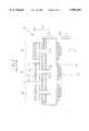
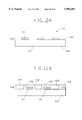
- FIG. 1there is shown a cross sectional view of an M ⁇ N electrodisplacive actuated mirror array 10 for use in an optical projection system, disclosed in a copending commonly owned application, U.S. Ser. No. 08/278,472, entitled “ELECTRODISPLACIVE ACTUATED MIRROR ARRAY", now U.S. Pat. No.
- 5,735,026,comprising: an active matrix 11 including a substrate 12 and an array of M ⁇ N transistors thereon; an array 13 of M ⁇ N electrodisplacive actuators 30, each of the electrodisplacive actuators 30 including a pair of actuating members 14, 15, a pair of bias electrodes 16, 17, and a common signal electrode 18; an array 19 of M ⁇ N hinges 31, each of the hinges 31 fitted in each of the electrodisplacive actuators 30; an array 20 of M ⁇ N connecting terminals 22, each of the connecting terminals 22 being used for electrically connecting each of the signal electrodes 18 with the active matrix 11; and an array 21 of M ⁇ N mirrors 23, each of the mirrors 23 being mounted on top of each of the M ⁇ N hinges 31.
- a primary object of the present inventionis to provide a method for manufacturing an array of M ⁇ N actuated mirrors, which dispenses with the use of a thin electrodiplacive ceramic wafer.
- an array of M ⁇ N thin film actuated mirrorsfor use in an optical projection system, the array comprising: an active matrix including a substrate, an array of M ⁇ N transistors and an array of M ⁇ N connecting terminals; an array of M ⁇ N thin film actuating structures, each of the actuating structures including a first and a second actuating parts, the first and second actuating parts being identically structured, each of the first and second actuating parts being provided with a top and a bottom surfaces, a proximal and a distal ends, each of the first and second actuating parts having at least a thin film layer of a motion-inducing material including a top and a bottom surfaces and a first and a second electrode with the first electrode being placed on the top surface of the motion-inducing thin film layer, and the second electrode, on the bottom surface of the motion-inducing thin film layer, wherein an electrical signal applied across the motion-inducing thin film layer between the first and second
- a novel method for manufacturing an array of M ⁇ N actuated mirrors for use in an optical projection systemcomprising the steps of: (a) providing an active matrix having a top and a bottom surfaces, the active matrix including a substrate, an array of M ⁇ N transistors and an array of M ⁇ N connecting terminals; (b) forming a first supporting layer on the top surface of the active matrix, the first supporting layer including an array of M ⁇ N pedestals corresponding to the array of M ⁇ N supporting members in the array of M ⁇ N thin film actuated mirrors and a first sacrificial area; (c) treating the first sacrificial area of the first supporting layer to be removable; (d) depositing a first thin film electrode layer on the first supporting layer; (e) providing a thin film motion-inducing layer on the first thin film electrode layer; (f) forming a second thin film electrode layer on the thin film motion-inducing layer; (g) pattern
- FIG. 1shows a cross sectional view of an array of M ⁇ N electrodisplacive actuated mirrors previously disclosed
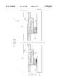
- FIG. 2represents a cross sectional view of M ⁇ N thin film actuated mirrors in accordance with the first preferred embodiment of the present invention
- FIG. 3illustrates a detailed cross sectional view of the inventive thin film actuated mirror array of the first embodiment, shown in FIG. 2;
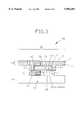
- FIG. 4depicts a top view of the inventive thin film actuated mirror array of the first embodiment, shown in FIG. 2;
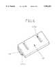
- FIG. 5represents a detailed perspective view of the inventive thin film actuated mirror array of the first embodiment, shown in FIG. 2;
- FIG. 6offers another possible mirror layer configuration for the first embodiment
- FIG. 7discloses a cross sectional view of a thin film actuated mirror of the first embodiment in an actuated state
- FIG. 8provides a cross sectional view of a thin film actuated mirror of the second embodiment having a bimorph structure
- FIG. 9is a cross sectional view of an array of M ⁇ N thin film actuated mirrors in accordance with the third preferred embodiment of the present invention.
- FIG. 10displays a detailed cross sectional view of the inventive film actuated mirror array of the third embodiment, shown in FIG. 9;
- FIG. 11describes a perspective view of the inventive thin film actuated mirror array of the third embodiment, shown in FIG. 9.
- FIGS. 12A to 12Jreproduce schematic cross sectional views setting forth the manufacturing steps for the first embodiment in accordance with the present invention.
- FIGS. 2 to 12there are provided schematic cross sectional views of the inventive array of M ⁇ N thin film actuated mirrors for use in an optical projection system and method for the manufacture thereof, wherein M and N are integers, in accordance with preferred embodiments of the present invention. It should by noted that like parts appearing in FIGS. 2 to 12 are represented by like reference numerals.
- FIG. 2there is illustrated a cross sectional view of a first embodiment of an array 50 of M ⁇ N thin film actuated mirrors 51, comprising an active matrix 52, an array 53 of M ⁇ N thin film actuating structures 54, an array 55 of M ⁇ N supporting members 56, and an array 57 of M ⁇ N mirror layers 58.
- FIG. 3represents a detailed cross sectional view of the thin film actuated mirror array 50, shown in FIG. 2.
- Tne active matrix 52includes a substrate 59, an array of M ⁇ N transistors (not shown) and an array 60 of M ⁇ N connecting terminals 61.
- Each of the actuating structures 54includes identically structured first actuating and second actuating parts 62(a), 62(b), wherein each actuating part, e.g., 62(a), is provided with a top and a bottom surfaces 63, 64, a proximal and a distal ends 65, 66.
- Each actuating part, e.g., 62(a),further has at least a thin film layer 67 of a motion-inducing material, e.g., a piezoelectric material, an electrostrictive material or a magnetostrictive material, including a top and a bottom surface 68, 69 and a first and a second electrodes 70, 71 with the first electrode 70 being placed on the top surface 68 of the motion-inducing layer 67 and the second electrode 71, on the bottom surface 71 of the motion-inducing layer 67.
- the motion-inducing layer 67is made of a piezoelectric material., e.g., lead zirconium titanate (PZT), it must be poled.
- the first and second electrodesare made of a metal such as gold (Au) or silver (Ag).
- Each of the M ⁇ N supporting members 56is used for holding the first and the second actuating parts 62(a), 62(b) of each of the actuating structures 54 in place and also for electrically connecting the second electrode 71 in the first and second actuating parts 62(a), 62(b) in each of actuating structures 54 with the corresponding connecting terminal 61 on the active matrix 52 by being provided with a conduit 99 made of an electrically conductive material, e.g., a metal.
- each of the first and second actuating parts 62(a), 62(b) in each of the actuating structures 54are cantilevered from each of the supporting members 56 by being mounted on the top surface 73 of each of the supporting members 56 at the bottom surface 64 of each of the first and second actuating parts 62(a), 62(b) in each of the actuating structures 54 at the proximal end 65 thereof, and the bottom surface 74 of each of the supporting members 56 is placed on top of the active matrix 52.
- each of the mirror layer 58including a mirror 75 for reflecting light beams and a supporting layer 76 having a top surface 77, is provided with a first side 78, a second opposing side 79 and a center portion 80 located therebetween, as illustrated in FIG. 4.
- the first side 78 andc the second opposing side 79 of each of the mirror layers 58are placed on top of the first and second actuating parts 62(a), 62(b) of each of the actuating structures 54, respectively.
- FIGS. 5 and 6there are shown a perspective view of a thin film actuated mirror 51 of the first embodiment and another possible mirror layer configuration for the array 50 of M ⁇ N thin film actuated mirrors 51, respectively.
- the material making up the supporting layer 76 in each of the mirror layers 58can be also light reflecting, e.g., aluminum (Al), which will allow the top surface 77 thereof to function also as the mirror 75 in each of the thin film actuated mirrors 51.
- Alaluminum
- the inventive array 50 of thin film actuated mirrors 51can function equally well by having the top and bottom surfaces 68, 69 of the motion-inducing thin film layer 67 in each of the actuating structures 54 covered completely with the first and second electrodes 70, 71 or by having either one of the top and bottom surfaces 68, 69 of the motion-inducing thin film layer 67 in each of the actuating structures 54 covered partially with the first and second electrodes 70, 71.
- FIGS. 3 and 7there are illustrated in FIGS. 3 and 7 an array 50 of M ⁇ N thin film actuated mirrors 51 comprising an array 53 of M ⁇ N actuating structures 54, made of a piezoelectric material, e.g., PZT.
- An electric fieldis applied across the piezoelectric thin film layer 67 located between the first and second electrodes 70, 71 in each of the actuating parts 62(a), 62(b) in each of the actuating structures 54.
- the application of the electric fieldwill either cause the piezoelectric material to contract or expand, depending on the polarity of the electric field with respect to the poling of the piezoelectric material.
- the polarity of the piezoelectric materialcorresponds to the polarity of the applied electric field, causing the piezoelectric material to contract.
- the first and second actuating parts 62(a), 62(b) of each of actuating structure 54bend downward, as shown in FIG. 7, thereby tilting the first side 78 and the second opposing side 79 of the mirror layer 58 downward at an angle.
- the center portion 80 of the mirror layer 58remains planar, and as a result, the effective length of the mirror layer 58 is the entire length of the center portion 80 of the mirror layer 58.
- the effective length of the mirror layer 58is equal to a length less the length of the portion of the actuating structure 54 secured to the supporting member 56.
- an electric field of a reverse polaritymay be applied across the motion-inducing thin film piezoelectric layer 67, causing the piezoelectric material to expand.
- the actuating structure 54bends upward (not shown).
- the light impinging the mirror layer 58 of the upwardly actuated mirror 51is deflected at a smaller angle than the light deflected from the unactuated actuated mirror 51 shown in FIG. 3.
- FIG. 8a cross sectional view of a second embodiment of an array 100 of M ⁇ N thin film actuated mirrors 101, wherein the second embodiment is similar to the first embodiment except that each of the first and second actuating parts 62(a), 62(b) in each of the actuating structures 54 is of a bimorph structure, including a first electrode 70, a second electrode 71, an intermediate metal layers 87 an upper motion-inducing thin film layer 89 having a top and a bottom surfaces 90, 91 and a lower motion-inducing thin film layer 92 provided with a top and bottom surfaces 93, 94.
- the upper and lower motion-inducing thin film layers 89, 92are separated by the intermediate metal layer 87, the first electrode 70 being placed on the top surface 90 of the upper motion-inducing thin film layer 89, and the second electrode 71, on the bottom surface 94 of the lower motion-inducing thin film layer 92.
- the upper and lower motion-inducing thin film layers 89, 92 in each of the actuating structures 54are made of a piezoelectric material, an electrostrictive ceramic or a magnetostrictive ceramic.
- the upper and lower motion-inducing thin film layers 89, 92are made of a piezoelectric material, e.g., a piezoelectric ceramic or a piezoelectric polymer, the upper and lower motion-inducing thin film layers 89, 92 must be poled in such a way that the polarization direction of piezoelectric material in the upper motion-inducing thin film layer 89 is opposite from that of the lower motion-inducing thin film layer 92.
- the upper and lower motion-inducing layers 89, 90 in the array 100 of M ⁇ N thin film actuated mirrors 101 shown in FIG. 8are made of a piezoelectric material, e.g., PZT.
- PZTpiezoelectric material
- the actuating parts 62(a), 62(b) in each of the actuating structures 54will bend upward. In this situation, the impinging light is deflected at a smaller angle from the actuated mirror 51 than the deflected light from the unactuated actuated mirror 51.
- the actuating structure 54will bend downward. In this situation, the impinging light is deflected at a larger angle from the actuated mirror 51 than the deflected light from the unactuated actuated mirror 51.
- FIG. 9a schematic cross sectional view of a third embodiment of an array 200 of M ⁇ N thin film actuated mirrors 201.
- the third embodimentis similar to the first embodiment except that the first and second actuating parts 62(a), 62(b) of each of the actuating structures 54 lack the supporting layer 76 in the mirror layer 58. Instead, they are provided with an elastic layer 202 located on the bottom surface 69 of the motion-inducing layer 67, as shown in FIG. 10.
- an elastic layeris provided in an actuated mirror, the motion-inducing and elastic layers are usually separated by a layer of an expensive electrically conducting metal, e.g., platinum (Pt) to improve adhesion therebetween.
- Ptplatinum
- the thermal expansion coefficient of the materials making up the elastic layer and the motion-inducing layeris drastically different each other and the interface between the elastic layer and the electrically conductive metal layer or the interface between the motion-inducing laver and the electrically conductive layer are weak, they will lead to a peeling of the electrically conductive metal layer, thereby reducing the overall performance of the actuated mirror.
- a possible solution to this problemis to form the elastic and motion-inducing layers with the materials having the same structure, e.g., perovskite. Since the materials making up the elastic and motion-inducing layers are similar structurally, it will better adhesivity therebetween to thereby eliminate the need for forming of the electrically conductive metal layer and also allow an easier control of strain energy therebetween.
- the material making up the elastic layeris characterized by a high dielectric constant (.di-elect cons.) and a low piezoelectric constant (d).
- the first electrodeis made of a light reflecting material. e.g., Al
- the mirror layer 58can be omitted. In such a case the first electrode will also function as the mirror layer 58.
- FIGS. 12A to 12Jthere are illustrated in FIGS. 12A to 12J the manufacturing steps involved in manufacturing of the first embodiment of the present invention.
- the process for manufacturing the first embodimenti.e., the array 50 of M ⁇ N thin film actuated mirror 51, wherein M ⁇ N are integers, begins with the preparation of the active matrix 52, having the top and a bottom surfaces 102, 103, comprising the substrate 59, the array of M ⁇ N transistors (not shown) and the array 104 of M ⁇ N connecting terminals 105, as illustrated in FIG. 12A.
- a first supporting layer 106including an array 107 of M ⁇ N pedestals 108 corresponding to the array 55 of M ⁇ N supporting members 56 and a first sacrificial area 109, wherein the first supporting layer 106 is formed by: depositing a first sacrificial layer (not shown) on the entirety of the top surface 102 of the active matrix 52; forming an array of M ⁇ N empty slots (not shown), to thereby generated the first sacrificial area 109, each of the empty slots being located around each of the M ⁇ N connecting terminals 61; and providing a pedestal 108 in each of the empty slots, as shown in FIG. 12B.
- the first sacrificial layeris formed by using a sputtering method, the array of empty slots, using an etching method, and the pedestals, using a sputtering or a chemical vapor deposition (CVD) method, followed by an etching method.
- the sacrificial area 109 of the first supporting layer 106is then treated so as to be removable later using an etching method or the application of chemicals.
- an electrically conductive materiale.g., tungsten (W)
- a first thin film electrode layer 111made of an electrically conducting material, e.g., Au, is deposited on the first supporting layer 106.
- a thin film motion-inducing layer 112, made of a motion-inducing material, e.g., PZT, and a second thin film electrode layer 113are then formed on the first thin film electrode layer 111.
- the first thin film electrode layer 111, the thin film motion-inducing layer 112 and the second thin film electrode layer 113are patterned into an array 53 of M ⁇ N actuating structures 54 and an empty area (not shown) surrounding each of the actuating structures 54, wherein each of the actuating structures 54 includes the first and second actuating parts 62(a), 62(b), as shown in FIG. 12E.
- a second sacrificial layer 114is formed on the empty area surrounding each of the actuating structures 54, as described in FIG. 12F.
- the second sacrificial layer 114is then treated so as to be removable later.
- the sacrificial layer 114is then patterned into an array 115 of M ⁇ N sacrificial members 116. Subsequently a second supporting layer 117 and a light reflecting layer 119 comprising the mirror layer 58 are successively deposited on top of the array 53 of M ⁇ N actuating structures 54 and the second sacrificial layer 116 patterned previously, as illustrated in FIG. 12H.
- the light reflecting layer 119 and the second supporting layer 117are then patterned into an array 57 of M ⁇ N mirror layers 58, as depicted in FIG. 12I.
- the thin film layers of the electrically conducting, the motion-inducing, and the light reflecting materialsmay be deposited and patterned with the known thin film techniques, such as sputtering, sol-gel, evaporation, etching and micro-machining.
- the first sacrificial area 109 and the array 115 of M ⁇ N sacrificial members 116are then removed or dissolved by the application of chemical to thereby form said array 50 of M ⁇ N thin film actuated mirrors 51, as depicted in FIG. 12J.
- the fabrication of the second embodimentis similar to that of the first embodiment except that it requires two additional steps, the additional steps being the formation of an additional motion-inducing layer and an intermediate metal layer.
- each of the first and second actuating parts 62(a), 62(b) in each of the actuating structures 54is provided with an elastic layer 202 on the bottom surface of the motion inducing layer 67 while missing the supporting layer 76, the manufacturing step for the third embodiment are essentially the same as those of the first embodiment with the orders being changed slightly.
- the second electrode layeris made of a light reflecting material, e.g., Al, the step involved in forming of the light reflecting layer 119 can also be omitted form the overall manufacturing steps.
Landscapes
- Physics & Mathematics (AREA)
- General Physics & Mathematics (AREA)
- Optics & Photonics (AREA)
- Engineering & Computer Science (AREA)
- Multimedia (AREA)
- Signal Processing (AREA)
- Mechanical Light Control Or Optical Switches (AREA)
- Optical Elements Other Than Lenses (AREA)
- Mounting And Adjusting Of Optical Elements (AREA)
- Transforming Electric Information Into Light Information (AREA)
- Cathode-Ray Tubes And Fluorescent Screens For Display (AREA)
Abstract
Description
Claims (12)
Priority Applications (1)
| Application Number | Priority Date | Filing Date | Title |
|---|---|---|---|
| US09/150,747US5984481A (en) | 1993-11-16 | 1998-09-10 | Array of thin film actuated mirrors for use in an optical projection system and method for the manufacture thereof |
Applications Claiming Priority (8)
| Application Number | Priority Date | Filing Date | Title |
|---|---|---|---|
| KR93-24397 | 1993-11-16 | ||
| KR1019930024397AKR970006693B1 (en) | 1993-11-16 | 1993-11-16 | An optical path regulating apparatus of projection type of image display |
| KR93024395AKR970006691B1 (en) | 1993-11-16 | 1993-11-16 | A manufacturing method of an optical path regulating apparatus |
| KR93-24395 | 1993-11-16 | ||
| KR93-31716 | 1993-12-30 | ||
| KR1019930031716AKR970008400B1 (en) | 1993-12-30 | 1993-12-30 | Structure of Light Path Adjusting Device of Projection-type Image Display Device and Manufacturing Method Thereof |
| US08/340,762US5835293A (en) | 1993-11-16 | 1994-11-16 | Array of thin film actuated mirrors for use in an optical projection system and method for the manufacture thereof |
| US09/150,747US5984481A (en) | 1993-11-16 | 1998-09-10 | Array of thin film actuated mirrors for use in an optical projection system and method for the manufacture thereof |
Related Parent Applications (1)
| Application Number | Title | Priority Date | Filing Date |
|---|---|---|---|
| US08/340,762ContinuationUS5835293A (en) | 1993-11-16 | 1994-11-16 | Array of thin film actuated mirrors for use in an optical projection system and method for the manufacture thereof |
Publications (1)
| Publication Number | Publication Date |
|---|---|
| US5984481Atrue US5984481A (en) | 1999-11-16 |
Family
ID=27349019
Family Applications (3)
| Application Number | Title | Priority Date | Filing Date |
|---|---|---|---|
| US08/340,762Expired - Fee RelatedUS5835293A (en) | 1993-11-16 | 1994-11-16 | Array of thin film actuated mirrors for use in an optical projection system and method for the manufacture thereof |
| US09/150,773Expired - LifetimeUS6030083A (en) | 1993-11-16 | 1998-09-10 | Array of thin film actuated mirrors for use in an optical projection system and method for the manufacture thereof |
| US09/150,747Expired - LifetimeUS5984481A (en) | 1993-11-16 | 1998-09-10 | Array of thin film actuated mirrors for use in an optical projection system and method for the manufacture thereof |
Family Applications Before (2)
| Application Number | Title | Priority Date | Filing Date |
|---|---|---|---|
| US08/340,762Expired - Fee RelatedUS5835293A (en) | 1993-11-16 | 1994-11-16 | Array of thin film actuated mirrors for use in an optical projection system and method for the manufacture thereof |
| US09/150,773Expired - LifetimeUS6030083A (en) | 1993-11-16 | 1998-09-10 | Array of thin film actuated mirrors for use in an optical projection system and method for the manufacture thereof |
Country Status (16)
| Country | Link |
|---|---|
| US (3) | US5835293A (en) |
| EP (1) | EP0653657B1 (en) |
| JP (1) | JP3253304B2 (en) |
| CN (1) | CN1047904C (en) |
| AU (1) | AU693139B2 (en) |
| BR (1) | BR9408054A (en) |
| CA (1) | CA2176347A1 (en) |
| CZ (1) | CZ287202B6 (en) |
| DE (1) | DE69423070T2 (en) |
| ES (1) | ES2145086T3 (en) |
| HU (1) | HU220515B1 (en) |
| IT (1) | IT1271062B (en) |
| PL (1) | PL175809B1 (en) |
| RU (1) | RU2125347C1 (en) |
| TW (1) | TW266328B (en) |
| WO (1) | WO1995014351A1 (en) |
Cited By (5)
| Publication number | Priority date | Publication date | Assignee | Title |
|---|---|---|---|---|
| WO2001056066A1 (en)* | 2000-01-28 | 2001-08-02 | Reflectivity, Inc. | A method for forming a micromechanical device |
| KR20030060622A (en)* | 2002-01-10 | 2003-07-16 | 주식회사 대우일렉트로닉스 | Method for manufacturing thin-film micromirror array-actuated |
| US20040015691A1 (en)* | 2002-04-22 | 2004-01-22 | Collette William C. | Frame-level fibre channel CRC on switching platform |
| US20050002087A1 (en)* | 2003-06-21 | 2005-01-06 | Gareth Knowles | Thin, nearly wireless adaptive optical device |
| CN108519672A (en)* | 2012-11-29 | 2018-09-11 | 卡尔蔡司Smt有限责任公司 | Device at least one of actuated optical system optical element |
Families Citing this family (20)
| Publication number | Priority date | Publication date | Assignee | Title |
|---|---|---|---|---|
| JP3471156B2 (en)* | 1995-05-30 | 2003-11-25 | シャープ株式会社 | Image shift mechanism and imaging device |
| US6969635B2 (en)* | 2000-12-07 | 2005-11-29 | Reflectivity, Inc. | Methods for depositing, releasing and packaging micro-electromechanical devices on wafer substrates |
| US6849471B2 (en)* | 2003-03-28 | 2005-02-01 | Reflectivity, Inc. | Barrier layers for microelectromechanical systems |
| KR980003662A (en)* | 1996-06-28 | 1998-03-30 | 배순훈 | Thin film type optical path adjusting device having a large driving angle |
| JPH11514105A (en)* | 1996-08-13 | 1999-11-30 | テーウー エレクトロニクス カンパニー リミテッド | Thin-film optical path adjusting device and method of manufacturing the same |
| US5949568A (en)* | 1996-12-30 | 1999-09-07 | Daewoo Electronics Co., Ltd. | Array of thin film actuated mirrors having a levelling member |
| WO1998033327A1 (en)* | 1997-01-23 | 1998-07-30 | Daewoo Electronics Co., Ltd. | Thin film actuated mirror array in an optical projection system and method for manufacturing the same |
| CA2278624A1 (en)* | 1997-01-23 | 1998-07-30 | Daewoo Electronics Co., Ltd. | Thin film actuated mirror array in an optical projection system and method for manufacturing the same |
| RU2180158C2 (en)* | 1997-01-23 | 2002-02-27 | Дэу Электроникс Ко., Лтд. | Thin-film matrix of controlled mirrors for optical projection system and its manufacturing process |
| KR19980069199A (en)* | 1997-02-27 | 1998-10-26 | 배순훈 | Thin film type optical path adjusting device and its manufacturing method which can improve the light efficiency |
| WO1999023832A1 (en)* | 1997-10-31 | 1999-05-14 | Daewoo Electronics Co., Ltd. | Method for manufacturing thin film actuated mirror array in an optical projection system |
| US6965468B2 (en) | 2003-07-03 | 2005-11-15 | Reflectivity, Inc | Micromirror array having reduced gap between adjacent micromirrors of the micromirror array |
| US6947201B2 (en) | 2003-12-08 | 2005-09-20 | Xinetics, Inc. | Transverse electrodisplacive actuator array |
| JP4552606B2 (en)* | 2004-11-10 | 2010-09-29 | パナソニック株式会社 | Piezoelectric actuator and light sweep device using the same |
| US20090122428A1 (en)* | 2007-11-09 | 2009-05-14 | Nikon Corporation | Reflective optical elements exhibiting multimetallic-like self-correction of distortions caused by heating |
| TWI389016B (en)* | 2008-08-26 | 2013-03-11 | Acer Inc | Integrated pixel structure, integrated touch panel lcd device and method of controlling the same |
| US8654434B2 (en)* | 2010-07-20 | 2014-02-18 | Oclaro (New Jersey), Inc. | WSS with pixel gap compensation |
| KR102001460B1 (en)* | 2013-03-18 | 2019-07-19 | 삼성디스플레이 주식회사 | Optical module for laser beam shaking |
| WO2016124253A1 (en) | 2015-02-06 | 2016-08-11 | Optotune Ag | Optical device for enhancing resolution of an image |
| CN114779464A (en)* | 2022-05-24 | 2022-07-22 | 北京有竹居网络技术有限公司 | Optical signal modulator, control method and projection device |
Citations (26)
| Publication number | Priority date | Publication date | Assignee | Title |
|---|---|---|---|---|
| US1985424A (en)* | 1933-03-23 | 1934-12-25 | Ici Ltd | Alkylene-oxide derivatives of polyhydroxyalkyl-alkylamides |
| US2016962A (en)* | 1932-09-27 | 1935-10-08 | Du Pont | Process for producing glucamines and related products |
| US2703798A (en)* | 1950-05-25 | 1955-03-08 | Commercial Solvents Corp | Detergents from nu-monoalkyl-glucamines |
| US2920529A (en)* | 1952-05-23 | 1960-01-12 | Blythe Richard | Electronic control of optical and near-optical radiation |
| US3544201A (en)* | 1968-01-02 | 1970-12-01 | Gen Telephone & Elect | Optical beam deflector |
| US3614677A (en)* | 1966-04-29 | 1971-10-19 | Ibm | Electromechanical monolithic resonator |
| US3758199A (en)* | 1971-11-22 | 1973-09-11 | Sperry Rand Corp | Piezoelectrically actuated light deflector |
| US4441791A (en)* | 1980-09-02 | 1984-04-10 | Texas Instruments Incorporated | Deformable mirror light modulator |
| US4518976A (en)* | 1982-11-17 | 1985-05-21 | Konishiroku Photo Industry Co., Ltd. | Recording apparatus |
| US4979789A (en)* | 1989-06-02 | 1990-12-25 | Aura Systems, Inc. | Continuous source scene projector |
| EP0419853A2 (en)* | 1989-09-28 | 1991-04-03 | Texas Instruments Incorporated | Spatial light modulator |
| WO1991009503A1 (en)* | 1989-12-11 | 1991-06-27 | Aura Systems, Inc. | Television display system for modulating projected beams' intensity |
| US5032906A (en)* | 1989-07-12 | 1991-07-16 | Aura Systems, Inc. | Intensity calibration method for scene projector |
| US5035475A (en)* | 1990-03-15 | 1991-07-30 | Aura Systems, Inc. | Unique modulation television |
| US5085497A (en)* | 1990-03-16 | 1992-02-04 | Aura Systems, Inc. | Method for fabricating mirror array for optical projection system |
| US5138309A (en)* | 1990-04-03 | 1992-08-11 | Aura Systems, Inc. | Electronic switch matrix for a video display system |
| US5150205A (en)* | 1989-11-01 | 1992-09-22 | Aura Systems, Inc. | Actuated mirror optical intensity modulation |
| US5159225A (en)* | 1991-10-18 | 1992-10-27 | Aura Systems, Inc. | Piezoelectric actuator |
| US5185660A (en)* | 1989-11-01 | 1993-02-09 | Aura Systems, Inc. | Actuated mirror optical intensity modulation |
| WO1993008501A1 (en)* | 1991-10-18 | 1993-04-29 | Aura Systems, Inc. | Scene projector |
| US5209119A (en)* | 1990-12-12 | 1993-05-11 | Regents Of The University Of Minnesota | Microdevice for sensing a force |
| US5218512A (en)* | 1991-08-16 | 1993-06-08 | Rohm Co., Ltd. | Ferroelectric device |
| US5247222A (en)* | 1991-11-04 | 1993-09-21 | Engle Craig D | Constrained shear mode modulator |
| US5260798A (en)* | 1989-11-01 | 1993-11-09 | Aura Systems, Inc. | Pixel intensity modulator |
| US5281888A (en)* | 1992-03-17 | 1994-01-25 | Ngk Insulators, Ltd. | Piezoelectric/electrostrictive element having auxiliary electrode disposed between piezoelectric/electrostrictive layer and substrate |
| US5481396A (en)* | 1994-02-23 | 1996-01-02 | Aura Systems, Inc. | Thin film actuated mirror array |
Family Cites Families (4)
| Publication number | Priority date | Publication date | Assignee | Title |
|---|---|---|---|---|
| US4639788A (en)* | 1984-12-07 | 1987-01-27 | New York Institute Of Technology | Video display method and apparatus |
| US5090795A (en)* | 1987-10-22 | 1992-02-25 | Hughes Aircraft Company | Integrated adaptive optics apparatus |
| US5022745A (en)* | 1989-09-07 | 1991-06-11 | Massachusetts Institute Of Technology | Electrostatically deformable single crystal dielectrically coated mirror |
| DE4011805A1 (en)* | 1990-04-12 | 1991-10-17 | Hoechst Ag | METHOD FOR PRODUCING A SHOCK-STABILIZED LIQUID CRYSTAL CIRCUIT AND DISPLAY DEVICE |
- 1994
- 1994-11-15CACA002176347Apatent/CA2176347A1/ennot_activeAbandoned
- 1994-11-15DEDE69423070Tpatent/DE69423070T2/ennot_activeExpired - Lifetime
- 1994-11-15CZCZ19961413Apatent/CZ287202B6/ennot_activeIP Right Cessation
- 1994-11-15WOPCT/KR1994/000164patent/WO1995014351A1/enactiveIP Right Grant
- 1994-11-15JPJP51435395Apatent/JP3253304B2/ennot_activeExpired - Lifetime
- 1994-11-15ESES94118035Tpatent/ES2145086T3/ennot_activeExpired - Lifetime
- 1994-11-15EPEP94118035Apatent/EP0653657B1/ennot_activeExpired - Lifetime
- 1994-11-15HUHU9601201Apatent/HU220515B1/ennot_activeIP Right Cessation
- 1994-11-15BRBR9408054Apatent/BR9408054A/ennot_activeApplication Discontinuation
- 1994-11-15CNCN94194178Apatent/CN1047904C/ennot_activeExpired - Lifetime
- 1994-11-15PLPL94314420Apatent/PL175809B1/enunknown
- 1994-11-15RURU96113083Apatent/RU2125347C1/ennot_activeIP Right Cessation
- 1994-11-15AUAU11215/95Apatent/AU693139B2/ennot_activeCeased
- 1994-11-15ITITMI942309Apatent/IT1271062B/enactiveIP Right Grant
- 1994-11-16USUS08/340,762patent/US5835293A/ennot_activeExpired - Fee Related
- 1994-11-18TWTW083110725Apatent/TW266328B/zhactive
- 1998
- 1998-09-10USUS09/150,773patent/US6030083A/ennot_activeExpired - Lifetime
- 1998-09-10USUS09/150,747patent/US5984481A/ennot_activeExpired - Lifetime
Patent Citations (28)
| Publication number | Priority date | Publication date | Assignee | Title |
|---|---|---|---|---|
| US2016962A (en)* | 1932-09-27 | 1935-10-08 | Du Pont | Process for producing glucamines and related products |
| US1985424A (en)* | 1933-03-23 | 1934-12-25 | Ici Ltd | Alkylene-oxide derivatives of polyhydroxyalkyl-alkylamides |
| US2703798A (en)* | 1950-05-25 | 1955-03-08 | Commercial Solvents Corp | Detergents from nu-monoalkyl-glucamines |
| US2920529A (en)* | 1952-05-23 | 1960-01-12 | Blythe Richard | Electronic control of optical and near-optical radiation |
| US3614677A (en)* | 1966-04-29 | 1971-10-19 | Ibm | Electromechanical monolithic resonator |
| US3544201A (en)* | 1968-01-02 | 1970-12-01 | Gen Telephone & Elect | Optical beam deflector |
| US3758199A (en)* | 1971-11-22 | 1973-09-11 | Sperry Rand Corp | Piezoelectrically actuated light deflector |
| US4441791A (en)* | 1980-09-02 | 1984-04-10 | Texas Instruments Incorporated | Deformable mirror light modulator |
| US4518976A (en)* | 1982-11-17 | 1985-05-21 | Konishiroku Photo Industry Co., Ltd. | Recording apparatus |
| US4979789A (en)* | 1989-06-02 | 1990-12-25 | Aura Systems, Inc. | Continuous source scene projector |
| US5032906A (en)* | 1989-07-12 | 1991-07-16 | Aura Systems, Inc. | Intensity calibration method for scene projector |
| EP0419853A2 (en)* | 1989-09-28 | 1991-04-03 | Texas Instruments Incorporated | Spatial light modulator |
| US5185660A (en)* | 1989-11-01 | 1993-02-09 | Aura Systems, Inc. | Actuated mirror optical intensity modulation |
| US5126836A (en)* | 1989-11-01 | 1992-06-30 | Aura Systems, Inc. | Actuated mirror optical intensity modulation |
| US5260798A (en)* | 1989-11-01 | 1993-11-09 | Aura Systems, Inc. | Pixel intensity modulator |
| US5150205A (en)* | 1989-11-01 | 1992-09-22 | Aura Systems, Inc. | Actuated mirror optical intensity modulation |
| US5245369A (en)* | 1989-11-01 | 1993-09-14 | Aura Systems, Inc. | Scene projector |
| WO1991009503A1 (en)* | 1989-12-11 | 1991-06-27 | Aura Systems, Inc. | Television display system for modulating projected beams' intensity |
| US5035475A (en)* | 1990-03-15 | 1991-07-30 | Aura Systems, Inc. | Unique modulation television |
| US5085497A (en)* | 1990-03-16 | 1992-02-04 | Aura Systems, Inc. | Method for fabricating mirror array for optical projection system |
| US5138309A (en)* | 1990-04-03 | 1992-08-11 | Aura Systems, Inc. | Electronic switch matrix for a video display system |
| US5209119A (en)* | 1990-12-12 | 1993-05-11 | Regents Of The University Of Minnesota | Microdevice for sensing a force |
| US5218512A (en)* | 1991-08-16 | 1993-06-08 | Rohm Co., Ltd. | Ferroelectric device |
| WO1993008501A1 (en)* | 1991-10-18 | 1993-04-29 | Aura Systems, Inc. | Scene projector |
| US5159225A (en)* | 1991-10-18 | 1992-10-27 | Aura Systems, Inc. | Piezoelectric actuator |
| US5247222A (en)* | 1991-11-04 | 1993-09-21 | Engle Craig D | Constrained shear mode modulator |
| US5281888A (en)* | 1992-03-17 | 1994-01-25 | Ngk Insulators, Ltd. | Piezoelectric/electrostrictive element having auxiliary electrode disposed between piezoelectric/electrostrictive layer and substrate |
| US5481396A (en)* | 1994-02-23 | 1996-01-02 | Aura Systems, Inc. | Thin film actuated mirror array |
Cited By (7)
| Publication number | Priority date | Publication date | Assignee | Title |
|---|---|---|---|---|
| WO2001056066A1 (en)* | 2000-01-28 | 2001-08-02 | Reflectivity, Inc. | A method for forming a micromechanical device |
| KR20030060622A (en)* | 2002-01-10 | 2003-07-16 | 주식회사 대우일렉트로닉스 | Method for manufacturing thin-film micromirror array-actuated |
| US20040015691A1 (en)* | 2002-04-22 | 2004-01-22 | Collette William C. | Frame-level fibre channel CRC on switching platform |
| US20050002087A1 (en)* | 2003-06-21 | 2005-01-06 | Gareth Knowles | Thin, nearly wireless adaptive optical device |
| US7281808B2 (en) | 2003-06-21 | 2007-10-16 | Qortek, Inc. | Thin, nearly wireless adaptive optical device |
| CN108519672A (en)* | 2012-11-29 | 2018-09-11 | 卡尔蔡司Smt有限责任公司 | Device at least one of actuated optical system optical element |
| CN108519672B (en)* | 2012-11-29 | 2021-08-03 | 卡尔蔡司Smt有限责任公司 | Device for actuating at least one optical element in an optical system |
Also Published As
| Publication number | Publication date |
|---|---|
| ITMI942309A0 (en) | 1994-11-15 |
| PL314420A1 (en) | 1996-09-02 |
| HUT75801A (en) | 1997-05-28 |
| JP3253304B2 (en) | 2002-02-04 |
| RU2125347C1 (en) | 1999-01-20 |
| CN1047904C (en) | 1999-12-29 |
| AU1121595A (en) | 1995-06-06 |
| CZ141396A3 (en) | 1997-05-14 |
| ES2145086T3 (en) | 2000-07-01 |
| DE69423070D1 (en) | 2000-03-30 |
| EP0653657A1 (en) | 1995-05-17 |
| ITMI942309A1 (en) | 1996-05-15 |
| PL175809B1 (en) | 1999-02-26 |
| CZ287202B6 (en) | 2000-10-11 |
| DE69423070T2 (en) | 2000-07-13 |
| US6030083A (en) | 2000-02-29 |
| TW266328B (en) | 1995-12-21 |
| HU9601201D0 (en) | 1996-07-29 |
| EP0653657B1 (en) | 2000-02-23 |
| US5835293A (en) | 1998-11-10 |
| BR9408054A (en) | 1996-12-24 |
| AU693139B2 (en) | 1998-06-25 |
| WO1995014351A1 (en) | 1995-05-26 |
| IT1271062B (en) | 1997-05-26 |
| JPH09505157A (en) | 1997-05-20 |
| CN1135276A (en) | 1996-11-06 |
| CA2176347A1 (en) | 1995-05-26 |
| HU220515B1 (en) | 2002-03-28 |
Similar Documents
| Publication | Publication Date | Title |
|---|---|---|
| US5984481A (en) | Array of thin film actuated mirrors for use in an optical projection system and method for the manufacture thereof | |
| EP0652455B1 (en) | Thin film actuated mirror array for use in an optical projection system and method for the manufacture thereof | |
| US5900998A (en) | Thin film actuated mirror array and method for the manufacture thereof | |
| AU683363B2 (en) | Thin film actuated mirror array for use in an optical projection system and method for the manufacture thereof | |
| US5606452A (en) | Array of thin film actuated mirrors and method for the manufacture thereof | |
| US5627673A (en) | Array of thin film actuated mirrors for use in an optical projection system | |
| US5936757A (en) | Thin film actuated mirror array | |
| WO1996033437A1 (en) | Monomorph thin film actuated mirror array | |
| EP0718658B1 (en) | Low temperature formed thin film actuated mirror array |
Legal Events
| Date | Code | Title | Description |
|---|---|---|---|
| AS | Assignment | Owner name:DAEWOO ELECTRONICS CO., LTD., KOREA, REPUBLIC OF Free format text:ASSIGNMENT OF ASSIGNORS INTEREST;ASSIGNORS:MIN, YONG-KI;KIM, MYOUNG-JIN;REEL/FRAME:009450/0653 Effective date:19941101 | |
| STCF | Information on status: patent grant | Free format text:PATENTED CASE | |
| FEPP | Fee payment procedure | Free format text:PAYOR NUMBER ASSIGNED (ORIGINAL EVENT CODE: ASPN); ENTITY STATUS OF PATENT OWNER: LARGE ENTITY | |
| FPAY | Fee payment | Year of fee payment:4 | |
| FPAY | Fee payment | Year of fee payment:8 | |
| FEPP | Fee payment procedure | Free format text:PAYER NUMBER DE-ASSIGNED (ORIGINAL EVENT CODE: RMPN); ENTITY STATUS OF PATENT OWNER: LARGE ENTITY Free format text:PAYOR NUMBER ASSIGNED (ORIGINAL EVENT CODE: ASPN); ENTITY STATUS OF PATENT OWNER: LARGE ENTITY | |
| FPAY | Fee payment | Year of fee payment:12 | |
| AS | Assignment | Owner name:MAPLE VISION TECHNOLOGIES INC., CANADA Free format text:ASSIGNMENT OF ASSIGNORS INTEREST;ASSIGNOR:DAEWOO ELECTRONICS CORPORATION;REEL/FRAME:027437/0446 Effective date:20111215 | |
| AS | Assignment | Owner name:QUARTERHILL INC., CANADA Free format text:MERGER AND CHANGE OF NAME;ASSIGNORS:MAPLE VISION TECHNOLOGIES INC.;QUARTERHILL INC.;REEL/FRAME:042936/0464 Effective date:20170601 | |
| AS | Assignment | Owner name:WI-LAN INC., CANADA Free format text:ASSIGNMENT OF ASSIGNORS INTEREST;ASSIGNOR:QUARTERHILL INC.;REEL/FRAME:043181/0001 Effective date:20170601 |