US5984190A - Method and apparatus for identifying integrated circuits - Google Patents
Method and apparatus for identifying integrated circuitsDownload PDFInfo
- Publication number
- US5984190A US5984190AUS08/857,100US85710097AUS5984190AUS 5984190 AUS5984190 AUS 5984190AUS 85710097 AUS85710097 AUS 85710097AUS 5984190 AUS5984190 AUS 5984190A
- Authority
- US
- United States
- Prior art keywords
- integrated circuits
- identification
- optical
- identification code
- identification information
- Prior art date
- Legal status (The legal status is an assumption and is not a legal conclusion. Google has not performed a legal analysis and makes no representation as to the accuracy of the status listed.)
- Ceased
Links
- 238000000034methodMethods0.000titleclaimsabstractdescription28
- 230000003287optical effectEffects0.000claimsabstractdescription58
- 239000000853adhesiveSubstances0.000claimsdescription3
- 230000001070adhesive effectEffects0.000claimsdescription3
- 239000000758substrateSubstances0.000claims6
- 238000004519manufacturing processMethods0.000abstractdescription12
- 230000002596correlated effectEffects0.000abstractdescription2
- 238000012360testing methodMethods0.000description10
- 230000000875corresponding effectEffects0.000description5
- 239000004065semiconductorSubstances0.000description5
- 239000000523sampleSubstances0.000description4
- 238000013500data storageMethods0.000description2
- 238000004806packaging method and processMethods0.000description2
- JBRZTFJDHDCESZ-UHFFFAOYSA-NAsGaChemical compound[As]#[Ga]JBRZTFJDHDCESZ-UHFFFAOYSA-N0.000description1
- 229910001218Gallium arsenideInorganic materials0.000description1
- 239000000919ceramicSubstances0.000description1
- 238000010586diagramMethods0.000description1
- 239000000463materialSubstances0.000description1
- 238000012986modificationMethods0.000description1
- 230000004048modificationEffects0.000description1
- 229910021421monocrystalline siliconInorganic materials0.000description1
- 230000000007visual effectEffects0.000description1
Images
Classifications
- H—ELECTRICITY
- H01—ELECTRIC ELEMENTS
- H01L—SEMICONDUCTOR DEVICES NOT COVERED BY CLASS H10
- H01L21/00—Processes or apparatus adapted for the manufacture or treatment of semiconductor or solid state devices or of parts thereof
- H01L21/67—Apparatus specially adapted for handling semiconductor or electric solid state devices during manufacture or treatment thereof; Apparatus specially adapted for handling wafers during manufacture or treatment of semiconductor or electric solid state devices or components ; Apparatus not specifically provided for elsewhere
- H01L21/67005—Apparatus not specifically provided for elsewhere
- H01L21/67242—Apparatus for monitoring, sorting or marking
- H01L21/67282—Marking devices
- H—ELECTRICITY
- H01—ELECTRIC ELEMENTS
- H01L—SEMICONDUCTOR DEVICES NOT COVERED BY CLASS H10
- H01L23/00—Details of semiconductor or other solid state devices
- H01L23/544—Marks applied to semiconductor devices or parts, e.g. registration marks, alignment structures, wafer maps
- H—ELECTRICITY
- H01—ELECTRIC ELEMENTS
- H01L—SEMICONDUCTOR DEVICES NOT COVERED BY CLASS H10
- H01L2223/00—Details relating to semiconductor or other solid state devices covered by the group H01L23/00
- H01L2223/544—Marks applied to semiconductor devices or parts
- H01L2223/54413—Marks applied to semiconductor devices or parts comprising digital information, e.g. bar codes, data matrix
- H—ELECTRICITY
- H01—ELECTRIC ELEMENTS
- H01L—SEMICONDUCTOR DEVICES NOT COVERED BY CLASS H10
- H01L2223/00—Details relating to semiconductor or other solid state devices covered by the group H01L23/00
- H01L2223/544—Marks applied to semiconductor devices or parts
- H01L2223/54473—Marks applied to semiconductor devices or parts for use after dicing
- H01L2223/5448—Located on chip prior to dicing and remaining on chip after dicing
- H—ELECTRICITY
- H01—ELECTRIC ELEMENTS
- H01L—SEMICONDUCTOR DEVICES NOT COVERED BY CLASS H10
- H01L2223/00—Details relating to semiconductor or other solid state devices covered by the group H01L23/00
- H01L2223/544—Marks applied to semiconductor devices or parts
- H01L2223/54473—Marks applied to semiconductor devices or parts for use after dicing
- H01L2223/54486—Located on package parts, e.g. encapsulation, leads, package substrate
- H—ELECTRICITY
- H01—ELECTRIC ELEMENTS
- H01L—SEMICONDUCTOR DEVICES NOT COVERED BY CLASS H10
- H01L2924/00—Indexing scheme for arrangements or methods for connecting or disconnecting semiconductor or solid-state bodies as covered by H01L24/00
- H01L2924/0001—Technical content checked by a classifier
- H01L2924/0002—Not covered by any one of groups H01L24/00, H01L24/00 and H01L2224/00
Definitions
- This inventionrelates generally to integrated circuits, and more particularly to identification information for integrated circuits.
- Integrated circuitstypically are constructed on a single wafer of semiconductor material, such as monocrystalline silicon or gallium arsenide.
- the portion of the wafer occupied by a single one of the integrated circuitsis called a die.
- a series of tests(known as Probe) is performed in which the function of each die is tested.
- the test data collected for each dieis used in subsequent assembly/packaging steps to ensure that only properly functioning die are packaged as integrated circuit chips.
- each properly functioning dieis encapsulated (usually in plastic or ceramic) in a package having electric leads to form an integrated circuit chip. Subsequently, a series of testing operations is performed for each of the integrated circuit chips, with test data collected for each of the chips.
- the electronically readable identification informationis usually available only during those manufacturing procedures in which the integrated circuit is electrically tested. Also, retrieving the electronically readable identification information is usually done with a relatively sophisticated semiconductor testing apparatus, which necessarily makes physical contact with the integrated circuit chip in order to access the identifying information. There exist a number of manufacturing process steps during which such physical contact does not occur, and hence traceable identification of the individual integrated circuit chips through the various manufacturing processes is quite difficult. Also, once the manufacturer ships the integrated circuit chip to a customer, the unique identification information is not readily available.
- a method of identifying an integrated circuitin which the integrated circuit is both programmed with electronic identification information and marked with a corresponding machine-readable optical identification code.
- the integrated circuitmay be marked with an adhesive label, inscribed with a laser, or marked in any of a variety of suitable ways of displaying machine-readable optical identification codes.
- the integrated circuitmay include a plurality of programmable links which are programmed to store the electronic identification information, or include any of a variety of suitable adapted circuits for non-volatile data storage.
- the methodfurther includes the steps of reading the optical identification code and associating it with the corresponding electronic identification information.
- a look-up table or other suitable correlating meansmay be used for performing the association step.
- the optical identification codemay encode exactly the same data values as the electronic identification information.
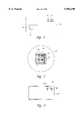
- FIG. 1is a block diagram depicting an integrated circuit which includes an identification circuit and a machine-readable optical mark.
- FIG. 2depicts a semiconductor wafer including a plurality of dies, each of which has a machine-readable optical mark.
- FIG. 3depicts a packaged integrated circuit chip which has a machine-readable optical mark.
- FIG. 1depicts an integrated circuit 10, which may be any of a wide variety of integrated circuits fabricated by conventional or newly developed methods.
- the integrated circuit 10includes a programmable identification circuit 12 having a bank of programmable links 13, for storing electronic identification information uniquely identifying the integrated circuit.
- the identification circuit 12can be any of a variety of circuits suitable for such purpose, whether currently well known or subsequently developed.
- the programmable linkscan be fuses, antifuses, or any of a wide variety of circuit elements suitable for non-volatile data storage, whether currently well known or subsequently developed.
- the method by which the identification circuit 12 is programmed to store the electronic identification information, as well as the method by which such information is retrieved from the identification circuit,can be any of a wide variety of methods for such purpose, whether currently well known or subsequently developed.
- U.S. Pat. No. 5,301,143 to Ohri et al.which is incorporated herein by reference, describes an example programmable identification circuit 12 and methods for storing/retrieving information to/from same.
- the integrated circuit 10also includes a machine-readable optical identification mark 14.
- the identification mark 14may be an adhesive label, a laser-scribed mark, or any of a wide variety of suitable marks.
- the identification mark 14displays an optical identification code 15 which corresponds with the electronic identification information stored in the programmable identification circuit 12.
- the optical identification code 15can be any of a wide variety of machine-readable optical identification codes, whether currently well known or subsequently developed.
- the optical identification code 15can be read by any of a wide variety of methods and with corresponding ones of a wide variety of optical code readers, whether currently well known or subsequently developed. For example, a particular optical identification code and a method and apparatus for reading and decoding the code are described in U.S. Pat. No. 5,389,770 to Ackley, which is incorporated herein by reference.
- FIG. 2depicts a semiconductor wafer 16 on which a plurality of integrated circuits 10 have been constructed, each on a corresponding one of a plurality of semiconductor dies 18.
- On each of the dies 18is a corresponding one of a plurality of the optical identification marks 14A, each having an optical identification code 15A which corresponds with the electronic identification information stored within the identification circuit 12 (see FIG. 1).
- FIG. 3depicts a packaged integrated circuit chip 20, within which one of the dies 18 (see FIG. 2) is encapsulated.
- the integrated circuit 10(see FIGS. 1 and 2) is electrically accessible via a plurality of electric leads 22.
- An outer surface of the packaged chip 20is marked with an optical identification mark 14B having an optical identification code 15B which corresponds with the electronic identification information stored within the identification circuit 12 (see FIG. 1).
- optical identification mark 14Bhaving an optical identification code 15B which corresponds with the electronic identification information stored within the identification circuit 12 (see FIG. 1).
- distinct reference numeralsare used to identify the optical identification marks and codes in FIGS. 1-3, indicating that various non-identical identification marks and codes may be used at different stages of the manufacturing process.
- the electronic identification informationis programmed into the identification circuit 12 during Probe testing of the various dies 18 included in the wafer 16.
- One or more of the identification marks 14-14Bcould then be produced to include an optical identification code which encodes data that is identical to the data stored in the identification circuit 12.
- the electronically accessible pattern of 1's and 0's stored in the identification circuit 12is the same as the optically accessible pattern of 1's and 0's encoded in one or more of the identification marks 14-14B.
- one or more of the identification marks 14-14Bcan be correlated, via a look-up table or other conventional correlation means, with the particular electronic identification data stored in the identification circuit 12--a more flexible approach than requiring identical data.
- integrated circuitshave included only the electronically accessible identification information, as well as visual marking information intended for human eyes.
- accurate identification of individual integrated circuitshas been available only during manufacturing processes in which the integrated circuit is electrically accessed.
- the present inventionprovides identification marks having an optical identification code associated with the electronic identification information, thereby providing convenient, accurate and traceable identification of individual integrated circuits during and following the manufacturing process.
- the ability to optically identify the integrated circuitavoids the need for physical contact, thereby minimizing the possibility of damage to the integrated circuit by the act of electronically reading the identification data--a common concern with current technology.
- the optical identification marks 14-14Bcan be any of a wide variety of such marks, and the method and apparatus for encoding optical identification information and reading such information can be any of a wide variety of suitable ones for such purpose.
- the identification circuit 12can be any of a wide variety of suitably adapted circuits, and the particular methods for programming and retrieving electronic identification information thereto and therefrom can be any of a wide variety of suitably adapted methods. It is the combination of both electrically accessible identification information and associated machine-readable optical identification codes which provides traceability of the integrated circuit through the manufacturing process, as well as after it has been shipped to a customer.
Landscapes
- Engineering & Computer Science (AREA)
- Physics & Mathematics (AREA)
- Condensed Matter Physics & Semiconductors (AREA)
- General Physics & Mathematics (AREA)
- Computer Hardware Design (AREA)
- Microelectronics & Electronic Packaging (AREA)
- Power Engineering (AREA)
- Manufacturing & Machinery (AREA)
- Semiconductor Integrated Circuits (AREA)
- Design And Manufacture Of Integrated Circuits (AREA)
- Testing Or Measuring Of Semiconductors Or The Like (AREA)
Abstract
Description
This invention relates generally to integrated circuits, and more particularly to identification information for integrated circuits.
Typically, many identical integrated circuits are constructed on a single wafer of semiconductor material, such as monocrystalline silicon or gallium arsenide. The portion of the wafer occupied by a single one of the integrated circuits is called a die. After completed fabrication of the integrated circuits, a series of tests (known as Probe) is performed in which the function of each die is tested. The test data collected for each die is used in subsequent assembly/packaging steps to ensure that only properly functioning die are packaged as integrated circuit chips.
Following the Probe test, the individual dies are separated from one another, and each properly functioning die is encapsulated (usually in plastic or ceramic) in a package having electric leads to form an integrated circuit chip. Subsequently, a series of testing operations is performed for each of the integrated circuit chips, with test data collected for each of the chips.
In order to properly correlate the various test results with the appropriate die or dies, accurate identification of each of the dies is required, both before and after packaging as an integrated circuit chip. The ability to identify particular dies can also be important following completed manufacture of the integrated circuit chip. For example, when an integrated circuit chip unexpectedly fails during later use, the manufacturer of the chip may wish to identify other potentially failing chips and the users of those chips.
Many of today's integrated circuits provide electronically readable identification information which is programmed into the integrated circuit itself--usually during Probe testing. Also, chip packages usually have an ink or laser-scribed mark which provides some useful information, such as date and country of manufacture, product and package types, speed and other test parameters, and manufacturing lot identification. However, information uniquely identifying the particular integrated circuit within a chip is included only in the electronically readable identification information.
The electronically readable identification information is usually available only during those manufacturing procedures in which the integrated circuit is electrically tested. Also, retrieving the electronically readable identification information is usually done with a relatively sophisticated semiconductor testing apparatus, which necessarily makes physical contact with the integrated circuit chip in order to access the identifying information. There exist a number of manufacturing process steps during which such physical contact does not occur, and hence traceable identification of the individual integrated circuit chips through the various manufacturing processes is quite difficult. Also, once the manufacturer ships the integrated circuit chip to a customer, the unique identification information is not readily available.
A method of identifying an integrated circuit is provided in which the integrated circuit is both programmed with electronic identification information and marked with a corresponding machine-readable optical identification code. The integrated circuit may be marked with an adhesive label, inscribed with a laser, or marked in any of a variety of suitable ways of displaying machine-readable optical identification codes. The integrated circuit may include a plurality of programmable links which are programmed to store the electronic identification information, or include any of a variety of suitable adapted circuits for non-volatile data storage.
The method further includes the steps of reading the optical identification code and associating it with the corresponding electronic identification information. A look-up table or other suitable correlating means may be used for performing the association step. Alternatively, the optical identification code may encode exactly the same data values as the electronic identification information.
FIG. 1 is a block diagram depicting an integrated circuit which includes an identification circuit and a machine-readable optical mark.
FIG. 2 depicts a semiconductor wafer including a plurality of dies, each of which has a machine-readable optical mark.
FIG. 3 depicts a packaged integrated circuit chip which has a machine-readable optical mark.
In the following description, certain specific details are set forth in order to provide a thorough understanding of embodiments of the present invention. It will be clear, however, to one skilled in the art that the present invention may be practiced without these details. In other instances, well-known circuits and structures have not been shown in detail in order not to unnecessarily obscure the description of the embodiments of the invention.
FIG. 1 depicts an integratedcircuit 10, which may be any of a wide variety of integrated circuits fabricated by conventional or newly developed methods. The integratedcircuit 10 includes aprogrammable identification circuit 12 having a bank ofprogrammable links 13, for storing electronic identification information uniquely identifying the integrated circuit. Theidentification circuit 12 can be any of a variety of circuits suitable for such purpose, whether currently well known or subsequently developed. The programmable links can be fuses, antifuses, or any of a wide variety of circuit elements suitable for non-volatile data storage, whether currently well known or subsequently developed. The method by which theidentification circuit 12 is programmed to store the electronic identification information, as well as the method by which such information is retrieved from the identification circuit, can be any of a wide variety of methods for such purpose, whether currently well known or subsequently developed. For example, U.S. Pat. No. 5,301,143 to Ohri et al., which is incorporated herein by reference, describes an exampleprogrammable identification circuit 12 and methods for storing/retrieving information to/from same.
The integratedcircuit 10 also includes a machine-readableoptical identification mark 14. Theidentification mark 14 may be an adhesive label, a laser-scribed mark, or any of a wide variety of suitable marks. Theidentification mark 14 displays anoptical identification code 15 which corresponds with the electronic identification information stored in theprogrammable identification circuit 12. Theoptical identification code 15 can be any of a wide variety of machine-readable optical identification codes, whether currently well known or subsequently developed. Theoptical identification code 15 can be read by any of a wide variety of methods and with corresponding ones of a wide variety of optical code readers, whether currently well known or subsequently developed. For example, a particular optical identification code and a method and apparatus for reading and decoding the code are described in U.S. Pat. No. 5,389,770 to Ackley, which is incorporated herein by reference.
FIG. 2 depicts asemiconductor wafer 16 on which a plurality of integratedcircuits 10 have been constructed, each on a corresponding one of a plurality of semiconductor dies 18. On each of thedies 18 is a corresponding one of a plurality of theoptical identification marks 14A, each having anoptical identification code 15A which corresponds with the electronic identification information stored within the identification circuit 12 (see FIG. 1). FIG. 3 depicts a packaged integratedcircuit chip 20, within which one of the dies 18 (see FIG. 2) is encapsulated. The integrated circuit 10 (see FIGS. 1 and 2) is electrically accessible via a plurality ofelectric leads 22. An outer surface of the packagedchip 20 is marked with anoptical identification mark 14B having anoptical identification code 15B which corresponds with the electronic identification information stored within the identification circuit 12 (see FIG. 1). Note that distinct reference numerals are used to identify the optical identification marks and codes in FIGS. 1-3, indicating that various non-identical identification marks and codes may be used at different stages of the manufacturing process.
Typically, the electronic identification information is programmed into theidentification circuit 12 during Probe testing of thevarious dies 18 included in thewafer 16. One or more of the identification marks 14-14B could then be produced to include an optical identification code which encodes data that is identical to the data stored in theidentification circuit 12. In other words, the electronically accessible pattern of 1's and 0's stored in theidentification circuit 12 is the same as the optically accessible pattern of 1's and 0's encoded in one or more of the identification marks 14-14B. Alternatively, one or more of the identification marks 14-14B can be correlated, via a look-up table or other conventional correlation means, with the particular electronic identification data stored in theidentification circuit 12--a more flexible approach than requiring identical data.
Those skilled in the art will appreciate a number of advantages achieved by the above-described embodiments of the present invention. Conventionally, integrated circuits have included only the electronically accessible identification information, as well as visual marking information intended for human eyes. Thus accurate identification of individual integrated circuits has been available only during manufacturing processes in which the integrated circuit is electrically accessed. In contrast, the present invention provides identification marks having an optical identification code associated with the electronic identification information, thereby providing convenient, accurate and traceable identification of individual integrated circuits during and following the manufacturing process. Also, the ability to optically identify the integrated circuit avoids the need for physical contact, thereby minimizing the possibility of damage to the integrated circuit by the act of electronically reading the identification data--a common concern with current technology.
As stated above, the optical identification marks 14-14B can be any of a wide variety of such marks, and the method and apparatus for encoding optical identification information and reading such information can be any of a wide variety of suitable ones for such purpose. Similarly, theidentification circuit 12 can be any of a wide variety of suitably adapted circuits, and the particular methods for programming and retrieving electronic identification information thereto and therefrom can be any of a wide variety of suitably adapted methods. It is the combination of both electrically accessible identification information and associated machine-readable optical identification codes which provides traceability of the integrated circuit through the manufacturing process, as well as after it has been shipped to a customer.
While certain embodiments of the invention have been described for purposes of illustration, various modifications may be made without deviating from the spirit and scope of the invention. Numerous variations are well within the scope of this invention, and accordingly, the invention is not limited except by the appended claims.
Claims (22)
1. A method of identifying a plurality of substantially identical integrated circuits formed on a common substrate, comprising the steps of:
programming each of the integrated circuits with respective electronic identification information distinguishing the integrated circuits from one another; and
marking each of the integrated circuits with respective optical identification code which corresponds with the respective electronic identification information;
reading the optical identification code on each of the integrated circuits; and
accessing a lookup table to associate the optical identification code on each of the integrated circuits with the corresponding electronic identification information.
2. The method of claim 1 wherein the step of programming each of the integrated circuits with electronic identification information includes the step of programming one of a plurality of programmable links.
3. The method of claim 1 wherein the step of marking each of the integrated circuits with optical identification code includes the step of placing an adhesive label on each of the integrated circuits.
4. The method of claim 1 wherein the step of marking each of the integrated circuits with optical identification code includes the step of inscribing a symbol on each of the integrated circuits.
5. The method of claim 1 wherein the step of marking each of the integrated circuits includes the step of marking respective portions of the substrate on which the integrated circuits are formed.
6. In a plurality of substantially identical integrated circuits formed on a common substrate, each of the integrated circuits including a programmable circuit for storing respective electronically readable identification code which distinguishes the integrated circuits from one another, a method of identifying the integrated circuits, comprising the steps of:
marking each of the integrated circuits with respective optical identification code;
accessing a lookup table to associate the optical identification code on each of the integrated circuits with the respective electronically readable identification code and
reading the optical identification code on each of the integrated circuits.
7. The method of claim 6 wherein the step of associating the optical identification code on each of the integrated circuits with the respective electronically readable identification code includes the steps of:
reading the electronically readable identification code stored in each of the integrated circuits;
reading the optical identification code marked on each of the integrated circuits; and
correlating the read electronically readable identification code with the read optical identification code for each of the integrated circuits.
8. The method of claim 6 wherein the step of associating the optical identification code on each of the integrated circuits with the respective electronically readable identification code includes the step of encoding identical data in the optical and electronically readable identification codes.
9. The method of claim 6 wherein the step of marking each of the integrated circuits includes the step of marking respective portions of the substrate on which the integrated circuits are formed.
10. A wafer comprising a plurality of dies, each die including an integrated circuit having a programmable identification circuit that stores identification data, and each die having an optical identification mark positioned thereon and encoding information corresponding to the identification data, optical identification mark on each die being accessed through a lookup table to correspond to the electronic identification information.
11. The wafer of claim 10 wherein the programmable identification circuit includes a plurality of programmable links.
12. The wafer of claim 10 wherein the optical identification mark encodes information identical to the identification data.
13. The wafer of claim 10 wherein the identification data uniquely distinguishes each of the dies.
14. A plurality of integrated circuit chips, each comprising:
a housing;
an integrated circuit enclosed within the housing and including an identification circuit that stores identification data distinguishing each of the integrated circuit chips from one another; and
an optical mark positioned on an exterior surface of the housing and encoding identification information being accessed through a lookup table to correspond to the identification data.
15. The integrated circuit chips of claim 14, further comprising electrical contacts connected to said housing and adapted to provide electrical connection between the integrated circuit and circuitry external to the housing.
16. The integrated circuit chips of claim 14 wherein the optical mark is a first optical mark encoding first identification information, and further comprising a second optical mark positioned on the integrated circuit enclosed within the housing and encoding second identification information corresponding to the identification data.
17. The integrated circuit chips of claim 16 wherein the first identification information is identical to the second identification information.
18. The integrated circuit chips of claim 14 wherein the identification information is the same as the identification data.
19. A method of identifying a plurality of substantially identical integrated circuits formed on a common substrate, each of the integrated circuits being formed on a respective one of a plurality of substrate dies, the method comprising:
programming each of the plurality of integrated circuits with respective electronic identification information for each of the integrated circuits; and
marking each of the dies with optical identification code which corresponds with the respective electronic identification information;
reading the optical identification code on each of the integrated circuits;
reading the electronic identification information from each of the integrated circuits; and
accessing a lookup table to associate the optical identification code on each of the integrated circuits with the corresponding electronic identification information.
20. The method of claim 19 wherein the electronic identification information is distinct for each of the integrated circuits.
21. The method of claim 19 wherein the optical identification code is distinct for each of the dies.
22. The method of claim 19 wherein the optical identification code and the electronic identification information include identical data.
Priority Applications (8)
| Application Number | Priority Date | Filing Date | Title |
|---|---|---|---|
| US08/857,100US5984190A (en) | 1997-05-15 | 1997-05-15 | Method and apparatus for identifying integrated circuits |
| KR1019997010556AKR100839003B1 (en) | 1997-05-15 | 1998-05-15 | Integrated circuit identification method and apparatus |
| EP98922427AEP1004142A1 (en) | 1997-05-15 | 1998-05-15 | Method and apparatus for identifying integrated circuits |
| AU74978/98AAU7497898A (en) | 1997-05-15 | 1998-05-15 | Method and apparatus for identifying integrated circuits |
| TW087107534ATW392232B (en) | 1997-05-15 | 1998-05-15 | Method and apparatus for identifying integrated circuits |
| PCT/US1998/010226WO1998052226A1 (en) | 1997-05-15 | 1998-05-15 | Method and apparatus for identifying integrated circuits |
| JP54967698AJP2001525993A (en) | 1997-05-15 | 1998-05-15 | Method and apparatus for integrated circuit identification |
| US09/998,594USRE40623E1 (en) | 1997-05-15 | 2001-11-16 | Method and apparatus for identifying integrated circuits |
Applications Claiming Priority (1)
| Application Number | Priority Date | Filing Date | Title |
|---|---|---|---|
| US08/857,100US5984190A (en) | 1997-05-15 | 1997-05-15 | Method and apparatus for identifying integrated circuits |
Related Child Applications (1)
| Application Number | Title | Priority Date | Filing Date |
|---|---|---|---|
| US09/998,594ReissueUSRE40623E1 (en) | 1997-05-15 | 2001-11-16 | Method and apparatus for identifying integrated circuits |
Publications (1)
| Publication Number | Publication Date |
|---|---|
| US5984190Atrue US5984190A (en) | 1999-11-16 |
Family
ID=25325182
Family Applications (2)
| Application Number | Title | Priority Date | Filing Date |
|---|---|---|---|
| US08/857,100CeasedUS5984190A (en) | 1997-05-15 | 1997-05-15 | Method and apparatus for identifying integrated circuits |
| US09/998,594Expired - Fee RelatedUSRE40623E1 (en) | 1997-05-15 | 2001-11-16 | Method and apparatus for identifying integrated circuits |
Family Applications After (1)
| Application Number | Title | Priority Date | Filing Date |
|---|---|---|---|
| US09/998,594Expired - Fee RelatedUSRE40623E1 (en) | 1997-05-15 | 2001-11-16 | Method and apparatus for identifying integrated circuits |
Country Status (7)
| Country | Link |
|---|---|
| US (2) | US5984190A (en) |
| EP (1) | EP1004142A1 (en) |
| JP (1) | JP2001525993A (en) |
| KR (1) | KR100839003B1 (en) |
| AU (1) | AU7497898A (en) |
| TW (1) | TW392232B (en) |
| WO (1) | WO1998052226A1 (en) |
Cited By (59)
| Publication number | Priority date | Publication date | Assignee | Title |
|---|---|---|---|---|
| US6268228B1 (en)* | 1999-01-27 | 2001-07-31 | International Business Machines Corporation | Electrical mask identification of memory modules |
| WO2001063670A3 (en)* | 2000-02-28 | 2002-01-31 | Ericsson Inc | Integrated circuit package with device specific data storage |
| WO2002013270A3 (en)* | 2000-08-10 | 2002-05-10 | Bosch Gmbh Robert | Semiconductor component and a method for identifying a semiconductor component |
| SG90756A1 (en)* | 1999-10-20 | 2002-08-20 | Tdk Corp | Method of reading mark and apparatus for the same |
| US20030042316A1 (en)* | 2001-08-31 | 2003-03-06 | Nobuyuki Teraura | Electronic device with ID tag, central processing unit with ID tag, and ID tag for electronic device |
| US6547151B1 (en)* | 1997-09-23 | 2003-04-15 | Stmicroelectronics S.R.L. | Currency note comprising an integrated circuit |
| US6555946B1 (en) | 2000-07-24 | 2003-04-29 | Motorola, Inc. | Acoustic wave device and process for forming the same |
| US6589856B2 (en) | 2001-08-06 | 2003-07-08 | Motorola, Inc. | Method and apparatus for controlling anti-phase domains in semiconductor structures and devices |
| US20030129836A1 (en)* | 2001-12-21 | 2003-07-10 | Takashi Sato | Semiconductor device and manufacturing method therefor |
| US20030157762A1 (en)* | 2000-06-28 | 2003-08-21 | Peterson Darin L. | Method and apparatus for marking microelectronic dies and microelectronic devices |
| US20030164611A1 (en)* | 2000-07-05 | 2003-09-04 | Walter Schneider | Antifalsification paper and security document produced therefrom |
| US6638838B1 (en) | 2000-10-02 | 2003-10-28 | Motorola, Inc. | Semiconductor structure including a partially annealed layer and method of forming the same |
| US6639249B2 (en) | 2001-08-06 | 2003-10-28 | Motorola, Inc. | Structure and method for fabrication for a solid-state lighting device |
| US20030205622A1 (en)* | 2000-09-13 | 2003-11-06 | Detlef Houdeau | Machine-readable label |
| US6646293B2 (en) | 2001-07-18 | 2003-11-11 | Motorola, Inc. | Structure for fabricating high electron mobility transistors utilizing the formation of complaint substrates |
| US20030223281A1 (en)* | 2002-05-29 | 2003-12-04 | Micron Technology, Inc. | Programable identification circuitry |
| US6667196B2 (en) | 2001-07-25 | 2003-12-23 | Motorola, Inc. | Method for real-time monitoring and controlling perovskite oxide film growth and semiconductor structure formed using the method |
| US6673646B2 (en) | 2001-02-28 | 2004-01-06 | Motorola, Inc. | Growth of compound semiconductor structures on patterned oxide films and process for fabricating same |
| US6673667B2 (en) | 2001-08-15 | 2004-01-06 | Motorola, Inc. | Method for manufacturing a substantially integral monolithic apparatus including a plurality of semiconductor materials |
| US6693298B2 (en) | 2001-07-20 | 2004-02-17 | Motorola, Inc. | Structure and method for fabricating epitaxial semiconductor on insulator (SOI) structures and devices utilizing the formation of a compliant substrate for materials used to form same |
| US6693033B2 (en) | 2000-02-10 | 2004-02-17 | Motorola, Inc. | Method of removing an amorphous oxide from a monocrystalline surface |
| US6709989B2 (en) | 2001-06-21 | 2004-03-23 | Motorola, Inc. | Method for fabricating a semiconductor structure including a metal oxide interface with silicon |
| US20040066575A1 (en)* | 2002-10-04 | 2004-04-08 | Taisuke Hirooka | Thin-film magnetic head wafer and method for manufacturing the wafer |
| US6731016B2 (en) | 2000-06-28 | 2004-05-04 | Micron Technology, Inc. | Method and apparatus for marking microelectronic dies and microelectronic devices |
| US6731221B1 (en)* | 1999-12-20 | 2004-05-04 | Intel Corporation | Electrically modifiable product labeling |
| WO2004055894A1 (en)* | 2002-12-17 | 2004-07-01 | Infineon Technologies Ag | Integrated semiconductor module comprising an identification region |
| US6795743B1 (en)* | 2000-09-18 | 2004-09-21 | Dell Products L.P. | Apparatus and method for electronically encoding an article with work-in-progress information |
| US6855992B2 (en) | 2001-07-24 | 2005-02-15 | Motorola Inc. | Structure and method for fabricating configurable transistor devices utilizing the formation of a compliant substrate for materials used to form the same |
| US6885065B2 (en) | 2002-11-20 | 2005-04-26 | Freescale Semiconductor, Inc. | Ferromagnetic semiconductor structure and method for forming the same |
| US6916717B2 (en) | 2002-05-03 | 2005-07-12 | Motorola, Inc. | Method for growing a monocrystalline oxide layer and for fabricating a semiconductor device on a monocrystalline substrate |
| US6918535B1 (en)* | 1998-07-27 | 2005-07-19 | Infineon Technologies Ag | Security paper, method and device for checking the authenticity of documents recorded thereon |
| SG114558A1 (en)* | 2001-06-27 | 2005-09-28 | Shinko Electric Ind Co | Wiring substrate having position information |
| US6965128B2 (en) | 2003-02-03 | 2005-11-15 | Freescale Semiconductor, Inc. | Structure and method for fabricating semiconductor microresonator devices |
| US6992321B2 (en) | 2001-07-13 | 2006-01-31 | Motorola, Inc. | Structure and method for fabricating semiconductor structures and devices utilizing piezoelectric materials |
| US7005717B2 (en) | 2000-05-31 | 2006-02-28 | Freescale Semiconductor, Inc. | Semiconductor device and method |
| US20060055535A1 (en)* | 2004-09-13 | 2006-03-16 | Shoei-Lai Chen | Method of building electronic label for electronic device |
| US20060063286A1 (en)* | 2004-09-23 | 2006-03-23 | Bidermann William R | Using a time invariant statistical process variable of a semiconductor chip as the chip identifier |
| US7019332B2 (en) | 2001-07-20 | 2006-03-28 | Freescale Semiconductor, Inc. | Fabrication of a wavelength locker within a semiconductor structure |
| US7020374B2 (en) | 2003-02-03 | 2006-03-28 | Freescale Semiconductor, Inc. | Optical waveguide structure and method for fabricating the same |
| US7045815B2 (en) | 2001-04-02 | 2006-05-16 | Freescale Semiconductor, Inc. | Semiconductor structure exhibiting reduced leakage current and method of fabricating same |
| US20060108412A1 (en)* | 1998-12-07 | 2006-05-25 | Chikashi Okamoto | Method of checking authenticity of sheet with built-in electronic circuit chip |
| US7067856B2 (en) | 2000-02-10 | 2006-06-27 | Freescale Semiconductor, Inc. | Semiconductor structure, semiconductor device, communicating device, integrated circuit, and process for fabricating the same |
| US7105866B2 (en) | 2000-07-24 | 2006-09-12 | Freescale Semiconductor, Inc. | Heterojunction tunneling diodes and process for fabricating same |
| US20060283961A1 (en)* | 2005-06-15 | 2006-12-21 | Fuji Photo Film Co., Ltd. | Method for recording identification information on semiconductor chip, and imaging device |
| US7161227B2 (en) | 2001-08-14 | 2007-01-09 | Motorola, Inc. | Structure and method for fabricating semiconductor structures and devices for detecting an object |
| US7169619B2 (en) | 2002-11-19 | 2007-01-30 | Freescale Semiconductor, Inc. | Method for fabricating semiconductor structures on vicinal substrates using a low temperature, low pressure, alkaline earth metal-rich process |
| US7211852B2 (en) | 2001-01-19 | 2007-05-01 | Freescale Semiconductor, Inc. | Structure and method for fabricating GaN devices utilizing the formation of a compliant substrate |
| US7342276B2 (en) | 2001-10-17 | 2008-03-11 | Freescale Semiconductor, Inc. | Method and apparatus utilizing monocrystalline insulator |
| US20080121709A1 (en)* | 2004-12-13 | 2008-05-29 | Tokyo Electron Limited | Semiconductor Chip With Identification Codes, Manufacturing Method Of The Chip And Semiconductor Chip Management System |
| US20090051027A1 (en)* | 2000-03-13 | 2009-02-26 | Megica Corporation | Method of Manufacture and Identification of Semiconductor Chip Marked For Identification with Internal Marking Indicia and Protection Thereof by Non-black Layer and Device Produced Thereby |
| US20100235652A1 (en)* | 2009-03-10 | 2010-09-16 | International Business Machines Corporation | Power supply identification using a modified power good signal |
| US8038538B2 (en) | 2004-06-04 | 2011-10-18 | Mattel, Inc. | Electronic device for enhancing an interactive experience with a tangible medium of expression |
| US20120322271A1 (en)* | 2011-06-15 | 2012-12-20 | Shen Wang | Identification of dies on a semiconductor wafer |
| US8415813B2 (en) | 2011-06-15 | 2013-04-09 | Truesense Imaging, Inc. | Identification of dies on a semiconductor wafer |
| US9305664B2 (en) | 2014-03-26 | 2016-04-05 | Texas Instruments Incorporated | Memory repair categorization tracking |
| US20170221871A1 (en)* | 2016-02-01 | 2017-08-03 | Octavo Systems Llc | Systems and methods for manufacturing electronic devices |
| US10062650B2 (en) | 2014-09-01 | 2018-08-28 | Mitsubishi Electric Corporation | Semiconductor device, and semiconductor chip having chip identification information |
| US20180342411A1 (en)* | 2017-03-16 | 2018-11-29 | Elenion Technologies, Llc | Chip identification system |
| US11276098B2 (en)* | 2017-10-25 | 2022-03-15 | Xilinx, Inc. | Database lookup using a scannable code for part selection |
Families Citing this family (14)
| Publication number | Priority date | Publication date | Assignee | Title |
|---|---|---|---|---|
| US6161213A (en)* | 1999-02-17 | 2000-12-12 | Icid, Llc | System for providing an integrated circuit with a unique identification |
| DE10044502A1 (en)* | 2000-09-08 | 2002-04-04 | Infineon Technologies Ag | Method and marking for marking integrated circuits |
| DE10216874A1 (en)* | 2002-04-17 | 2003-07-10 | Infineon Technologies Ag | Semiconductor chip and process for laying down information on it forms wafer level package with contacts and has optically readable identification on each chip |
| DE102006001601B4 (en) | 2006-01-11 | 2008-06-26 | Infineon Technologies Ag | Method for producing a semiconductor wafer with backside identification |
| DE112015003753T5 (en) | 2014-08-14 | 2017-06-29 | Octavo Systems Llc | IMPROVED SUBSTRATE FOR SYSTEM-IN-PACKAGE (SIP) DEVICES |
| WO2017040967A1 (en) | 2015-09-04 | 2017-03-09 | Octavo Systems Llc | Improved system using system in package components |
| US10714427B2 (en) | 2016-09-08 | 2020-07-14 | Asml Netherlands B.V. | Secure chips with serial numbers |
| US10418324B2 (en) | 2016-10-27 | 2019-09-17 | Asml Netherlands B.V. | Fabricating unique chips using a charged particle multi-beamlet lithography system |
| US11032910B2 (en) | 2017-05-01 | 2021-06-08 | Octavo Systems Llc | System-in-Package device ball map and layout optimization |
| US10470294B2 (en) | 2017-05-01 | 2019-11-05 | Octavo Systems Llc | Reduction of passive components in system-in-package devices |
| US11416050B2 (en) | 2017-05-08 | 2022-08-16 | Octavo Systems Llc | Component communications in system-in-package systems |
| US10714430B2 (en) | 2017-07-21 | 2020-07-14 | Octavo Systems Llc | EMI shield for molded packages |
| KR20200011142A (en) | 2018-07-24 | 2020-02-03 | 삼성전기주식회사 | Communication module and method for manufacturing the same |
| JP2022067888A (en)* | 2020-10-21 | 2022-05-09 | 国立研究開発法人産業技術総合研究所 | Method of assigning an individual identifier and an object having an individual identifier |
Citations (17)
| Publication number | Priority date | Publication date | Assignee | Title |
|---|---|---|---|---|
| DE3138085A1 (en)* | 1981-09-24 | 1983-04-07 | Siemens AG, 1000 Berlin und 8000 München | Process for marking peripheral systems on semiconductor wafers during the manufacture of semiconductor devices, in particular of integrated semiconductor circuits |
| DE3226733A1 (en)* | 1981-11-26 | 1983-07-07 | Softelec S.A., 1400 Yverdon | Integrated circuit |
| US4967381A (en)* | 1985-04-30 | 1990-10-30 | Prometrix Corporation | Process control interface system for managing measurement data |
| GB2244339A (en)* | 1990-05-23 | 1991-11-27 | Samsung Electronics Co Ltd | Integrated circuit chip having an identification circuit therein |
| EP0488053A1 (en)* | 1990-11-29 | 1992-06-03 | Tokyo Seimitsu Co.,Ltd. | Method for manufacturing a semiconductor chip |
| US5226118A (en)* | 1991-01-29 | 1993-07-06 | Prometrix Corporation | Data analysis system and method for industrial process control systems |
| EP0578410A2 (en)* | 1992-07-09 | 1994-01-12 | Advanced Micro Devices, Inc. | Programmable die identification circuits |
| US5294812A (en)* | 1990-09-14 | 1994-03-15 | Kabushiki Kaisha Toshiba | Semiconductor device having identification region for carrying out failure analysis |
| US5301143A (en)* | 1992-12-31 | 1994-04-05 | Micron Semiconductor, Inc. | Method for identifying a semiconductor die using an IC with programmable links |
| US5313174A (en)* | 1992-09-18 | 1994-05-17 | Rockwell International Corporation | 2:1 bandwidth, 4-way, combiner/splitter |
| US5380998A (en)* | 1990-08-15 | 1995-01-10 | International Business Machines Corporation | Single width bar code with end code providing bidirectionality |
| US5389770A (en)* | 1993-01-22 | 1995-02-14 | Intermec Corporation | Method and apparatus for decoding unresolved bar code profiles |
| US5420796A (en)* | 1993-12-23 | 1995-05-30 | Vlsi Technology, Inc. | Method of inspecting planarity of wafer surface after etchback step in integrated circuit fabrication |
| US5434870A (en)* | 1992-04-17 | 1995-07-18 | Unisys Corporation | Apparatus and method for verifying the authenticity of a circuit board |
| US5467304A (en)* | 1993-11-17 | 1995-11-14 | Nec Corporation | Semiconductor integrated circuit |
| US5511005A (en)* | 1994-02-16 | 1996-04-23 | Ade Corporation | Wafer handling and processing system |
| US5787174A (en)* | 1992-06-17 | 1998-07-28 | Micron Technology, Inc. | Remote identification of integrated circuit |
Family Cites Families (18)
| Publication number | Priority date | Publication date | Assignee | Title |
|---|---|---|---|---|
| JPS57122544A (en)* | 1981-01-23 | 1982-07-30 | Hitachi Ltd | Semiconductor device |
| JPH0793413B2 (en)* | 1987-03-09 | 1995-10-09 | 日本電気株式会社 | Method for manufacturing semiconductor device |
| US4904853A (en) | 1987-09-22 | 1990-02-27 | Kabushiki Kaisha Astex | Dual-function information-carrying sheet device |
| DE4124833A1 (en)* | 1990-07-28 | 1992-02-06 | Christian Berg | Labelling component for electronic modules - has mounted optical or EM absorbing reflecting or fluorescent elements providing code |
| US5129974A (en) | 1990-08-23 | 1992-07-14 | Colorcode Unlimited Corporation | Microlabelling system and method of making thin labels |
| ES2089556T3 (en)* | 1991-09-13 | 1996-10-01 | Rodney Arthur Stafford | ELECTRONIC SYSTEM FOR THE IDENTIFICATION OF ANIMALS. |
| JPH0684730A (en)* | 1992-08-31 | 1994-03-25 | Fujitsu Ltd | Method for manufacturing semiconductor device |
| US5360747A (en) | 1993-06-10 | 1994-11-01 | Xilinx, Inc. | Method of reducing dice testing with on-chip identification |
| US5801067A (en) | 1993-10-27 | 1998-09-01 | Ronald Shaw | Method for recording and identifying integrated circuit chips and the like |
| US5446447A (en)* | 1994-02-16 | 1995-08-29 | Motorola, Inc. | RF tagging system including RF tags with variable frequency resonant circuits |
| US5641164A (en) | 1994-10-13 | 1997-06-24 | The M2000 Group Inc. | Talking trading cards |
| US5743801A (en) | 1995-08-18 | 1998-04-28 | Welander; Paul M. | Collectable video sports card |
| US5742526A (en) | 1996-01-03 | 1998-04-21 | Micron Technology, Inc. | Apparatus and method for identifying an integrated device |
| US5748731A (en) | 1996-07-02 | 1998-05-05 | Shepherd; Henry G. | Electronic trading cards |
| US5949059A (en)* | 1996-12-09 | 1999-09-07 | International Business Machines Corporation | Tamper evident labelling system with embedded storage device |
| US5927512A (en)* | 1997-01-17 | 1999-07-27 | Micron Technology, Inc. | Method for sorting integrated circuit devices |
| US5962834A (en)* | 1997-03-17 | 1999-10-05 | Markman; Herbert L. | Inventory tracking and management apparatus with multi-function encoding unit |
| EP1770592B1 (en)* | 1998-08-14 | 2009-10-07 | 3M Innovative Properties Company | Method of interrogating a package bearing an RFID tag |
- 1997
- 1997-05-15USUS08/857,100patent/US5984190A/ennot_activeCeased
- 1998
- 1998-05-15AUAU74978/98Apatent/AU7497898A/ennot_activeAbandoned
- 1998-05-15JPJP54967698Apatent/JP2001525993A/enactivePending
- 1998-05-15TWTW087107534Apatent/TW392232B/ennot_activeIP Right Cessation
- 1998-05-15WOPCT/US1998/010226patent/WO1998052226A1/ennot_activeApplication Discontinuation
- 1998-05-15EPEP98922427Apatent/EP1004142A1/ennot_activeCeased
- 1998-05-15KRKR1019997010556Apatent/KR100839003B1/ennot_activeExpired - Fee Related
- 2001
- 2001-11-16USUS09/998,594patent/USRE40623E1/ennot_activeExpired - Fee Related
Patent Citations (18)
| Publication number | Priority date | Publication date | Assignee | Title |
|---|---|---|---|---|
| DE3138085A1 (en)* | 1981-09-24 | 1983-04-07 | Siemens AG, 1000 Berlin und 8000 München | Process for marking peripheral systems on semiconductor wafers during the manufacture of semiconductor devices, in particular of integrated semiconductor circuits |
| DE3226733A1 (en)* | 1981-11-26 | 1983-07-07 | Softelec S.A., 1400 Yverdon | Integrated circuit |
| US4967381A (en)* | 1985-04-30 | 1990-10-30 | Prometrix Corporation | Process control interface system for managing measurement data |
| GB2244339A (en)* | 1990-05-23 | 1991-11-27 | Samsung Electronics Co Ltd | Integrated circuit chip having an identification circuit therein |
| US5103166A (en)* | 1990-05-23 | 1992-04-07 | Samsung Electronics Co., Ltd. | Semiconductor integrated circuit chip having an identification circuit therein |
| US5380998A (en)* | 1990-08-15 | 1995-01-10 | International Business Machines Corporation | Single width bar code with end code providing bidirectionality |
| US5294812A (en)* | 1990-09-14 | 1994-03-15 | Kabushiki Kaisha Toshiba | Semiconductor device having identification region for carrying out failure analysis |
| EP0488053A1 (en)* | 1990-11-29 | 1992-06-03 | Tokyo Seimitsu Co.,Ltd. | Method for manufacturing a semiconductor chip |
| US5226118A (en)* | 1991-01-29 | 1993-07-06 | Prometrix Corporation | Data analysis system and method for industrial process control systems |
| US5434870A (en)* | 1992-04-17 | 1995-07-18 | Unisys Corporation | Apparatus and method for verifying the authenticity of a circuit board |
| US5787174A (en)* | 1992-06-17 | 1998-07-28 | Micron Technology, Inc. | Remote identification of integrated circuit |
| EP0578410A2 (en)* | 1992-07-09 | 1994-01-12 | Advanced Micro Devices, Inc. | Programmable die identification circuits |
| US5313174A (en)* | 1992-09-18 | 1994-05-17 | Rockwell International Corporation | 2:1 bandwidth, 4-way, combiner/splitter |
| US5301143A (en)* | 1992-12-31 | 1994-04-05 | Micron Semiconductor, Inc. | Method for identifying a semiconductor die using an IC with programmable links |
| US5389770A (en)* | 1993-01-22 | 1995-02-14 | Intermec Corporation | Method and apparatus for decoding unresolved bar code profiles |
| US5467304A (en)* | 1993-11-17 | 1995-11-14 | Nec Corporation | Semiconductor integrated circuit |
| US5420796A (en)* | 1993-12-23 | 1995-05-30 | Vlsi Technology, Inc. | Method of inspecting planarity of wafer surface after etchback step in integrated circuit fabrication |
| US5511005A (en)* | 1994-02-16 | 1996-04-23 | Ade Corporation | Wafer handling and processing system |
Cited By (77)
| Publication number | Priority date | Publication date | Assignee | Title |
|---|---|---|---|---|
| US6547151B1 (en)* | 1997-09-23 | 2003-04-15 | Stmicroelectronics S.R.L. | Currency note comprising an integrated circuit |
| US6918535B1 (en)* | 1998-07-27 | 2005-07-19 | Infineon Technologies Ag | Security paper, method and device for checking the authenticity of documents recorded thereon |
| US20060108412A1 (en)* | 1998-12-07 | 2006-05-25 | Chikashi Okamoto | Method of checking authenticity of sheet with built-in electronic circuit chip |
| US7309019B2 (en)* | 1998-12-07 | 2007-12-18 | Hitachi, Ltd. | Method of checking authenticity of sheet with built-in electronic circuit chip |
| US6570254B1 (en) | 1999-01-27 | 2003-05-27 | International Business Machines Corporation | Electrical mask identification of memory modules |
| US6268228B1 (en)* | 1999-01-27 | 2001-07-31 | International Business Machines Corporation | Electrical mask identification of memory modules |
| SG90756A1 (en)* | 1999-10-20 | 2002-08-20 | Tdk Corp | Method of reading mark and apparatus for the same |
| US6721443B1 (en) | 1999-10-20 | 2004-04-13 | Tdk Corporation | Method of reading mark and apparatus for the same |
| US6731221B1 (en)* | 1999-12-20 | 2004-05-04 | Intel Corporation | Electrically modifiable product labeling |
| US7067856B2 (en) | 2000-02-10 | 2006-06-27 | Freescale Semiconductor, Inc. | Semiconductor structure, semiconductor device, communicating device, integrated circuit, and process for fabricating the same |
| US6693033B2 (en) | 2000-02-10 | 2004-02-17 | Motorola, Inc. | Method of removing an amorphous oxide from a monocrystalline surface |
| WO2001063670A3 (en)* | 2000-02-28 | 2002-01-31 | Ericsson Inc | Integrated circuit package with device specific data storage |
| US20090051027A1 (en)* | 2000-03-13 | 2009-02-26 | Megica Corporation | Method of Manufacture and Identification of Semiconductor Chip Marked For Identification with Internal Marking Indicia and Protection Thereof by Non-black Layer and Device Produced Thereby |
| US7005717B2 (en) | 2000-05-31 | 2006-02-28 | Freescale Semiconductor, Inc. | Semiconductor device and method |
| US6731016B2 (en) | 2000-06-28 | 2004-05-04 | Micron Technology, Inc. | Method and apparatus for marking microelectronic dies and microelectronic devices |
| US6673692B2 (en)* | 2000-06-28 | 2004-01-06 | Micron Technology, Inc. | Method and apparatus for marking microelectronic dies and microelectronic devices |
| US6744144B2 (en) | 2000-06-28 | 2004-06-01 | Micron Technology, Inc. | Method and apparatus for marking microelectronic dies and microelectronic devices |
| US20030157762A1 (en)* | 2000-06-28 | 2003-08-21 | Peterson Darin L. | Method and apparatus for marking microelectronic dies and microelectronic devices |
| US20030164611A1 (en)* | 2000-07-05 | 2003-09-04 | Walter Schneider | Antifalsification paper and security document produced therefrom |
| US7105866B2 (en) | 2000-07-24 | 2006-09-12 | Freescale Semiconductor, Inc. | Heterojunction tunneling diodes and process for fabricating same |
| US6555946B1 (en) | 2000-07-24 | 2003-04-29 | Motorola, Inc. | Acoustic wave device and process for forming the same |
| US6750479B2 (en)* | 2000-08-10 | 2004-06-15 | Robert Bosch Gmbh | Semiconductor component and a method for identifying a semiconductor component |
| WO2002013270A3 (en)* | 2000-08-10 | 2002-05-10 | Bosch Gmbh Robert | Semiconductor component and a method for identifying a semiconductor component |
| US20030127718A1 (en)* | 2000-08-10 | 2003-07-10 | Frieder Haag | Semiconductor component and a method for identifying a semiconductor component |
| US20030205622A1 (en)* | 2000-09-13 | 2003-11-06 | Detlef Houdeau | Machine-readable label |
| US6795743B1 (en)* | 2000-09-18 | 2004-09-21 | Dell Products L.P. | Apparatus and method for electronically encoding an article with work-in-progress information |
| US6638838B1 (en) | 2000-10-02 | 2003-10-28 | Motorola, Inc. | Semiconductor structure including a partially annealed layer and method of forming the same |
| US7211852B2 (en) | 2001-01-19 | 2007-05-01 | Freescale Semiconductor, Inc. | Structure and method for fabricating GaN devices utilizing the formation of a compliant substrate |
| US6673646B2 (en) | 2001-02-28 | 2004-01-06 | Motorola, Inc. | Growth of compound semiconductor structures on patterned oxide films and process for fabricating same |
| US7045815B2 (en) | 2001-04-02 | 2006-05-16 | Freescale Semiconductor, Inc. | Semiconductor structure exhibiting reduced leakage current and method of fabricating same |
| US6709989B2 (en) | 2001-06-21 | 2004-03-23 | Motorola, Inc. | Method for fabricating a semiconductor structure including a metal oxide interface with silicon |
| SG114558A1 (en)* | 2001-06-27 | 2005-09-28 | Shinko Electric Ind Co | Wiring substrate having position information |
| US6992321B2 (en) | 2001-07-13 | 2006-01-31 | Motorola, Inc. | Structure and method for fabricating semiconductor structures and devices utilizing piezoelectric materials |
| US6646293B2 (en) | 2001-07-18 | 2003-11-11 | Motorola, Inc. | Structure for fabricating high electron mobility transistors utilizing the formation of complaint substrates |
| US7019332B2 (en) | 2001-07-20 | 2006-03-28 | Freescale Semiconductor, Inc. | Fabrication of a wavelength locker within a semiconductor structure |
| US6693298B2 (en) | 2001-07-20 | 2004-02-17 | Motorola, Inc. | Structure and method for fabricating epitaxial semiconductor on insulator (SOI) structures and devices utilizing the formation of a compliant substrate for materials used to form same |
| US6855992B2 (en) | 2001-07-24 | 2005-02-15 | Motorola Inc. | Structure and method for fabricating configurable transistor devices utilizing the formation of a compliant substrate for materials used to form the same |
| US6667196B2 (en) | 2001-07-25 | 2003-12-23 | Motorola, Inc. | Method for real-time monitoring and controlling perovskite oxide film growth and semiconductor structure formed using the method |
| US6589856B2 (en) | 2001-08-06 | 2003-07-08 | Motorola, Inc. | Method and apparatus for controlling anti-phase domains in semiconductor structures and devices |
| US6639249B2 (en) | 2001-08-06 | 2003-10-28 | Motorola, Inc. | Structure and method for fabrication for a solid-state lighting device |
| US7161227B2 (en) | 2001-08-14 | 2007-01-09 | Motorola, Inc. | Structure and method for fabricating semiconductor structures and devices for detecting an object |
| US6673667B2 (en) | 2001-08-15 | 2004-01-06 | Motorola, Inc. | Method for manufacturing a substantially integral monolithic apparatus including a plurality of semiconductor materials |
| US20030042316A1 (en)* | 2001-08-31 | 2003-03-06 | Nobuyuki Teraura | Electronic device with ID tag, central processing unit with ID tag, and ID tag for electronic device |
| US6873259B2 (en)* | 2001-08-31 | 2005-03-29 | Denso Corporation | Electronic device with ID tag, central processing unit with ID tag, and ID tag for electronic device |
| US7342276B2 (en) | 2001-10-17 | 2008-03-11 | Freescale Semiconductor, Inc. | Method and apparatus utilizing monocrystalline insulator |
| US20030129836A1 (en)* | 2001-12-21 | 2003-07-10 | Takashi Sato | Semiconductor device and manufacturing method therefor |
| US20050280129A1 (en)* | 2001-12-21 | 2005-12-22 | Yamaha Corporation | Semiconductor device and manufacturing method therefor |
| US6916717B2 (en) | 2002-05-03 | 2005-07-12 | Motorola, Inc. | Method for growing a monocrystalline oxide layer and for fabricating a semiconductor device on a monocrystalline substrate |
| US20060158916A1 (en)* | 2002-05-29 | 2006-07-20 | Micron Technology, Inc. | Programable identification circuitry |
| US20030223281A1 (en)* | 2002-05-29 | 2003-12-04 | Micron Technology, Inc. | Programable identification circuitry |
| US7046536B2 (en)* | 2002-05-29 | 2006-05-16 | Micron Technology, Inc. | Programable identification circuitry |
| US7471535B2 (en) | 2002-05-29 | 2008-12-30 | Micron Technology, Inc. | Programable identification circuitry |
| US20040066575A1 (en)* | 2002-10-04 | 2004-04-08 | Taisuke Hirooka | Thin-film magnetic head wafer and method for manufacturing the wafer |
| US7114239B2 (en)* | 2002-10-04 | 2006-10-03 | Neomax Co., Ltd. | Method for manufacturing a thin-film magnetic head wafer |
| US20060279879A1 (en)* | 2002-10-04 | 2006-12-14 | Neomax Co., Ltd. | Thin-film magnetic head wafer and method for manufacturing the wafer |
| US7474503B2 (en) | 2002-10-04 | 2009-01-06 | Hitachi Metals, Ltd. | Thin film magnetic head wafer with identification information |
| US7169619B2 (en) | 2002-11-19 | 2007-01-30 | Freescale Semiconductor, Inc. | Method for fabricating semiconductor structures on vicinal substrates using a low temperature, low pressure, alkaline earth metal-rich process |
| US6885065B2 (en) | 2002-11-20 | 2005-04-26 | Freescale Semiconductor, Inc. | Ferromagnetic semiconductor structure and method for forming the same |
| WO2004055894A1 (en)* | 2002-12-17 | 2004-07-01 | Infineon Technologies Ag | Integrated semiconductor module comprising an identification region |
| US7020374B2 (en) | 2003-02-03 | 2006-03-28 | Freescale Semiconductor, Inc. | Optical waveguide structure and method for fabricating the same |
| US6965128B2 (en) | 2003-02-03 | 2005-11-15 | Freescale Semiconductor, Inc. | Structure and method for fabricating semiconductor microresonator devices |
| US8038538B2 (en) | 2004-06-04 | 2011-10-18 | Mattel, Inc. | Electronic device for enhancing an interactive experience with a tangible medium of expression |
| US20060055535A1 (en)* | 2004-09-13 | 2006-03-16 | Shoei-Lai Chen | Method of building electronic label for electronic device |
| US7291507B2 (en)* | 2004-09-23 | 2007-11-06 | Pixim, Inc. | Using a time invariant statistical process variable of a semiconductor chip as the chip identifier |
| US20060063286A1 (en)* | 2004-09-23 | 2006-03-23 | Bidermann William R | Using a time invariant statistical process variable of a semiconductor chip as the chip identifier |
| US20080121709A1 (en)* | 2004-12-13 | 2008-05-29 | Tokyo Electron Limited | Semiconductor Chip With Identification Codes, Manufacturing Method Of The Chip And Semiconductor Chip Management System |
| US20060283961A1 (en)* | 2005-06-15 | 2006-12-21 | Fuji Photo Film Co., Ltd. | Method for recording identification information on semiconductor chip, and imaging device |
| US8108700B2 (en) | 2009-03-10 | 2012-01-31 | International Business Machines Corporation | Power supply identification using a modified power good signal |
| US20100235652A1 (en)* | 2009-03-10 | 2010-09-16 | International Business Machines Corporation | Power supply identification using a modified power good signal |
| US20120322271A1 (en)* | 2011-06-15 | 2012-12-20 | Shen Wang | Identification of dies on a semiconductor wafer |
| US8415175B2 (en)* | 2011-06-15 | 2013-04-09 | Truesense Imaging, Inc. | Identification of dies on a semiconductor wafer |
| US8415813B2 (en) | 2011-06-15 | 2013-04-09 | Truesense Imaging, Inc. | Identification of dies on a semiconductor wafer |
| US9305664B2 (en) | 2014-03-26 | 2016-04-05 | Texas Instruments Incorporated | Memory repair categorization tracking |
| US10062650B2 (en) | 2014-09-01 | 2018-08-28 | Mitsubishi Electric Corporation | Semiconductor device, and semiconductor chip having chip identification information |
| US20170221871A1 (en)* | 2016-02-01 | 2017-08-03 | Octavo Systems Llc | Systems and methods for manufacturing electronic devices |
| US20180342411A1 (en)* | 2017-03-16 | 2018-11-29 | Elenion Technologies, Llc | Chip identification system |
| US11276098B2 (en)* | 2017-10-25 | 2022-03-15 | Xilinx, Inc. | Database lookup using a scannable code for part selection |
Also Published As
| Publication number | Publication date |
|---|---|
| EP1004142A1 (en) | 2000-05-31 |
| JP2001525993A (en) | 2001-12-11 |
| KR100839003B1 (en) | 2008-06-18 |
| USRE40623E1 (en) | 2009-01-20 |
| AU7497898A (en) | 1998-12-08 |
| TW392232B (en) | 2000-06-01 |
| WO1998052226A1 (en) | 1998-11-19 |
| KR20010012597A (en) | 2001-02-15 |
Similar Documents
| Publication | Publication Date | Title |
|---|---|---|
| US5984190A (en) | Method and apparatus for identifying integrated circuits | |
| US10431551B2 (en) | Visual identification of semiconductor dies | |
| US6888159B2 (en) | Substrate mapping | |
| US7127365B2 (en) | Method for identifying a defective die site | |
| TW457611B (en) | Wafer-level package, a method of manufacturing thereof and a method of manufacturing semiconductor devices from such a wafer-level package | |
| US7561938B2 (en) | Method for using data regarding manufacturing procedures integrated circuits (ICS) have undergone, such as repairs, to select procedures the ICs will undergo, such as additional repairs | |
| KR19990006383A (en) | Semiconductor device and its information management system | |
| KR19980042525A (en) | Systems, methods, and apparatus for storing information during semiconductor manufacturing processes | |
| US6830941B1 (en) | Method and apparatus for identifying individual die during failure analysis | |
| KR100691678B1 (en) | Wafer Level Semiconductor Device Manufacturing Method and Semiconductor Device | |
| US12272643B2 (en) | Semiconductor device with identification structure, method for manufacturing and tracing production information thereof | |
| KR19980020175A (en) | A reel-type printed circuit board | |
| KR100228958B1 (en) | Die bonding apparatus | |
| KR100530396B1 (en) | Semiconductor device and manufacturing method therefor | |
| JP3736525B2 (en) | Semiconductor integrated circuit device and circuit board | |
| JP4127930B2 (en) | Semiconductor device, manufacturing method thereof, and manufacturing apparatus thereof | |
| KR100379084B1 (en) | Semiconductor Package Manufacturing Method | |
| JPS63239838A (en) | semiconductor equipment | |
| KR20000015597A (en) | Method for marking semiconductor package | |
| KR20030023268A (en) | Semiconductor Integrated Circuit Comprising an ID circuit Capable Of Storing Various ID Information | |
| JPH1187198A (en) | Semiconductor integrated circuit with memory for storing manufacture information, method for recording manufacturing state in the circuit and method for managing the circuit recorded with the information |
Legal Events
| Date | Code | Title | Description |
|---|---|---|---|
| AS | Assignment | Owner name:MICRON TECHNOLOGY, INC., IDAHO Free format text:ASSIGNMENT OF ASSIGNORS INTEREST;ASSIGNOR:NEVILL, LELAND R.;REEL/FRAME:008567/0039 Effective date:19970513 | |
| STCF | Information on status: patent grant | Free format text:PATENTED CASE | |
| CC | Certificate of correction | ||
| RF | Reissue application filed | Effective date:20011116 | |
| REMI | Maintenance fee reminder mailed | ||
| FPAY | Fee payment | Year of fee payment:4 | |
| SULP | Surcharge for late payment | ||
| FPAY | Fee payment | Year of fee payment:8 |