US5983363A - In-sheet transceiver testing - Google Patents
In-sheet transceiver testingDownload PDFInfo
- Publication number
- US5983363A US5983363AUS08/306,906US30690694AUS5983363AUS 5983363 AUS5983363 AUS 5983363AUS 30690694 AUS30690694 AUS 30690694AUS 5983363 AUS5983363 AUS 5983363A
- Authority
- US
- United States
- Prior art keywords
- signal
- transponder
- antenna
- sheet
- transceiver
- Prior art date
- Legal status (The legal status is an assumption and is not a legal conclusion. Google has not performed a legal analysis and makes no representation as to the accuracy of the status listed.)
- Expired - Lifetime
Links
Images

Classifications
- G—PHYSICS
- G06—COMPUTING OR CALCULATING; COUNTING
- G06K—GRAPHICAL DATA READING; PRESENTATION OF DATA; RECORD CARRIERS; HANDLING RECORD CARRIERS
- G06K19/00—Record carriers for use with machines and with at least a part designed to carry digital markings
- G06K19/06—Record carriers for use with machines and with at least a part designed to carry digital markings characterised by the kind of the digital marking, e.g. shape, nature, code
- G06K19/067—Record carriers with conductive marks, printed circuits or semiconductor circuit elements, e.g. credit or identity cards also with resonating or responding marks without active components
- G06K19/07—Record carriers with conductive marks, printed circuits or semiconductor circuit elements, e.g. credit or identity cards also with resonating or responding marks without active components with integrated circuit chips
- G06K19/0701—Record carriers with conductive marks, printed circuits or semiconductor circuit elements, e.g. credit or identity cards also with resonating or responding marks without active components with integrated circuit chips at least one of the integrated circuit chips comprising an arrangement for power management
- G—PHYSICS
- G01—MEASURING; TESTING
- G01R—MEASURING ELECTRIC VARIABLES; MEASURING MAGNETIC VARIABLES
- G01R31/00—Arrangements for testing electric properties; Arrangements for locating electric faults; Arrangements for electrical testing characterised by what is being tested not provided for elsewhere
- G01R31/01—Subjecting similar articles in turn to test, e.g. "go/no-go" tests in mass production; Testing objects at points as they pass through a testing station
- G—PHYSICS
- G01—MEASURING; TESTING
- G01R—MEASURING ELECTRIC VARIABLES; MEASURING MAGNETIC VARIABLES
- G01R31/00—Arrangements for testing electric properties; Arrangements for locating electric faults; Arrangements for electrical testing characterised by what is being tested not provided for elsewhere
- G01R31/28—Testing of electronic circuits, e.g. by signal tracer
- G01R31/282—Testing of electronic circuits specially adapted for particular applications not provided for elsewhere
- G01R31/2822—Testing of electronic circuits specially adapted for particular applications not provided for elsewhere of microwave or radiofrequency circuits
- G—PHYSICS
- G01—MEASURING; TESTING
- G01R—MEASURING ELECTRIC VARIABLES; MEASURING MAGNETIC VARIABLES
- G01R31/00—Arrangements for testing electric properties; Arrangements for locating electric faults; Arrangements for electrical testing characterised by what is being tested not provided for elsewhere
- G01R31/28—Testing of electronic circuits, e.g. by signal tracer
- G01R31/302—Contactless testing
- G01R31/3025—Wireless interface with the DUT
- G—PHYSICS
- G01—MEASURING; TESTING
- G01R—MEASURING ELECTRIC VARIABLES; MEASURING MAGNETIC VARIABLES
- G01R31/00—Arrangements for testing electric properties; Arrangements for locating electric faults; Arrangements for electrical testing characterised by what is being tested not provided for elsewhere
- G01R31/28—Testing of electronic circuits, e.g. by signal tracer
- G01R31/302—Contactless testing
- G01R31/303—Contactless testing of integrated circuits
- G—PHYSICS
- G06—COMPUTING OR CALCULATING; COUNTING
- G06K—GRAPHICAL DATA READING; PRESENTATION OF DATA; RECORD CARRIERS; HANDLING RECORD CARRIERS
- G06K7/00—Methods or arrangements for sensing record carriers, e.g. for reading patterns
- G06K7/0095—Testing the sensing arrangement, e.g. testing if a magnetic card reader, bar code reader, RFID interrogator or smart card reader functions properly
Definitions
- This inventionrelates to transponder testing and to test systems, fixtures, and methods for testing transponders.
- Such a transponderincludes a radio transceiver with a built-in antenna for receiving command message signals and for transmitting reply message signals.
- RFIDradio frequency identification
- Inexpensive transpondersfind application in systems for tracking material, personnel, and animals, inventory management, baggage handling, and the mail to name a few major areas.
- a transpondernecessarily includes a transceiver.
- Such transpondersmay include an integrated circuit transceiver, a battery, and a printed circuit antenna hermetically encapsulated in a laminated package about 1 inch square and approximately as thick as a mailing label or tag. In such a laminated package, manufacturing acceptance tests on each unit become difficult and costly.
- transpondersare inexpensively manufactured in sheets having for example 250 integrated circuit transceivers spaced apart in a row and column array between polymer films. Prior to use, the transponders are separated from each other by shearing the sheet between adjacent rows and columns. Conventional testing methods and apparatus cannot be used until the transponders are separated from each other.
- transponder testingfor manufacturing acceptance tests, incomplete testing may perpetrate unreliable tracking, inventory, and handling systems, increase the cost of maintaining such systems, and discourage further development and popular acceptance of transponder technology.
- a test system in one embodiment of the present inventionincludes a fixture, an interrogator, and a switch cooperating for testing a sheet containing a plurality of transceivers, each transceiver within a contour on the sheet.
- the fixturein one embodiment, admits a sheet of transceivers and surrounds each transceiver at its contour so that each transceiver is respectively enclosed within an enclosure.
- Within each enclosureis an antenna for so called "near-field" communication.
- the interrogatordetermines a command signal and evaluates reply signals from each transceiver.
- the switchis coupled in series between each antenna and the interrogator for selecting an antenna for transmitting the command signal and for receiving the reply signal.
- the fixtureisolates transceivers from each other so that multiple transceivers are tested simultaneously.
- each transceiverBy isolating each transceiver, interference from adjacent transceivers is minimized, transponder identity and location are not confused, and test transmissions are prevented from affecting external equipment including other test stations.
- testingis facilitated by isolating each transceiver at its contour.
- multiple transceiversare moved as a sheet and tested without further handling so that rapid testing is feasible and delays for physical alignment of the transceivers within the fixture is minimized.
- near-field testingis used to eliminate the need for large chambers.
- the transfer function of the antenna and detector portion of a transceiver receiveris tested.
- the present inventionis practiced according to a method in one embodiment which includes the steps of providing an enclosure that admits a sheet of transceivers, each transceiver formed within a respective region of the sheet, closing the enclosure to form an RF seal about each respective region, and operating each transceiver for receiving and transmitting signals.
- independent testing of individual transceiversis accomplished for in-sheet transceivers and multiple transceivers are tested simultaneously.
- far-field testsare used to confirm the test signal used in manufacturing tests.
- a method, in an alternate embodiment, for testing battery-operated transceiversincludes the step of transmitting a wake up signal to a transceiver. According to a first aspect of such a method, only transceivers under test are made operational so that battery power is conserved in other transceivers.
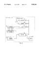
- FIG. 1is a plan view of a test system of the present invention.
- FIG. 2is a functional block diagram of the test system of FIG. 1.
- FIG. 3is a functional block diagram of a transponder of the present invention to be tested in the test system of FIG. 1.
- FIG. 4is a cross sectional view of fixture 15.
- a broad arrowsymbolically represents a group of signals that together signify a binary code.
- a group of bus linesis represented by a broad arrow because a binary value conveyed by the bus is signified by the signals on the several bus lines taken together at an instant in time.
- a group of signals having no binary coded relationshipis shown as a single line with an arrow.
- a single line between functional blocksrepresents one or more signals.
- FIG. 1is a plan view of a test system of the present invention.
- Test system 10provides manufacturing acceptance tests for an in-sheet transponder 12 provided on continuous roll 20 of laminated films. Transponders under test are located in fixture 15. Tested transponders are received on roll 22.
- Fixture 15is connected by cable 18 to subsystem 24 so that signals generated by instrumentation in subsystem 24 are coupled to fixture 15 and so that signals received in fixture 15 are coupled to instruments in subsystem 24 for analysis.
- Subsystem 24includes interrogator 25 and computer 86, cooperating for signal generation and analysis.
- Fixture 15is characterized, according to a method of the present invention, using a correlation to far-field testing. Characterization of a system, fixture, or circuit conventionally includes making measurements of characteristic features of its structure and operation.
- Transponders to be tested in an alternate embodimentare provided to fixture 15 in separated sheets, each sheet having an array of rows and columns of transponders.
- each sheethaving an array of rows and columns of transponders.
- about 250 transpondersare manufactured in a sheet measuring about 18 inches by about 24 inches.
- Test system 10also includes materials handling equipment, not shown, for supplying sheets or rolls of transponders for testing, for aligning transponders within fixture 15, and for receiving tested transponders for further manufacturing steps.
- materials handling equipmentnot shown, for supplying sheets or rolls of transponders for testing, for aligning transponders within fixture 15, and for receiving tested transponders for further manufacturing steps.
- individual tested transpondersare separated (singulated) from the sheet in which testing occurred and are provided on an adhesive backing for distribution as tape-and-reel components or ready-to-use articles such as baggage tags, inventory labels, or badges, to name a few feasible applications.
- Transponder 12is a radio frequency identification (RFID) device of the type described in U.S. patent application Ser. No. 07/990,918 by Snodgrass et al. filed Dec. 15, 1992, incorporated herein by reference.
- RFIDradio frequency identification
- transponder 12is about 1 inch square, includes a lithium battery, an integrated circuit transceiver, and an antenna packaged using thin film and lamination techniques.
- FIG. 2is a functional block diagram of a test system of the present invention.
- Test system 10includes six major functional elements: operator console 26, test system computer 86, interrogator 25, radio frequency (RF) switch 92, fixture 15, and material handling apparatus 90.
- operator console 26operator console 26
- test system computer 86test system computer 86
- interrogator 25radio frequency (RF) switch 92
- fixture 15fixture 15
- material handling apparatus 90material handling apparatus 90.
- test system computer 86directs material handling apparatus 90 to align a sheet of transponders (not shown) within fixture 15. Alignment assures that each transponder is isolated from other transponders in a manner to be discussed with reference to FIG. 4.
- alignmentincludes automatic recognition by video camera of guide marks on the sheet and control of stepper motors according to software performed by computer 86 or in an alternate embodiment by a computer in material handling apparatus 90.
- alignmentincludes the location of the fixture relative to the sheet so that the fixture, the sheet, or both can be repositioned to accomplish proper alignment.
- computer 86directs RF switch 92 for independently testing individual transponders.
- one transponderis tested at a time.
- multiple interrogatorsare coordinated to test multiple transponders simultaneously. Independent transponder operation during simultaneous testing of multiple transponders is accomplished in part by isolation provided by fixture 15.
- interrogator 25particularly interrogator central processing unit (CPU) 84, to generate and transmit via transmitter 82 command messages through switches 91 and 92, and to receive and interpret reply messages generated by that transponder that are conveyed through RF switch 92 and switch 91 to receiver 83.
- Interrogator 25is of the type described in U.S. patent application Ser. No. 07/990,918 by Snodgrass et al. filed Dec. 15, 1992, incorporated herein by reference.
- Switch 91 and switch 92are coax switches, common in the RF testing art. In alternate embodiments, switch 91 is eliminated and command and reply messages are separated by communication techniques known in the art, for example separation by time division or use of different frequency bands or different modulation techniques.
- a test of the sensitivity of the receiver portion of the transceiver portion of a transponder under testincludes transmitting from interrogator 25 a test signal, for example, a command message at a test power level. Transponders that fail to respond by transmitting a proper reply message fail the test at a first point.
- the reply messageincludes a measurement of the signal strength seen by the receiver portion of the transponder under test. Transponders that report measurements of received signal strength that do not exceed an expected signal strength fail the test at a second point. By setting both test points as requirements, the population of tested transponders is of higher quality because marginal units are rejected. Therefore, the determination of the test power level and the expected signal strength are important to production and application economics.
- Fixture 15surrounds each transponder so that each transceiver's antenna is within one enclosure.
- the enclosuresurrounds an entire transponder and a small volume of ambient air so that the enclosure forms a cavity.
- only the transceiver's antennais enclosed.
- the small volumeis filled with potting material so that, for example, the cleanliness of the enclosure and the position of the antenna within the enclosure are maintained.
- the potting materialincludes polyimide.
- conventional potting materials and conventional materials used for films for encapsulating the transponderare used. The power level to be used for each enclosure depends on the materials and dimensions of the enclosure and the transponder.
- test power levelappropriate for one of several enclosures formed by fixture 15
- far-field test resultsare correlated to conventional characterization tests of the transponder, potting material (if any), and the enclosure.
- characterization testsBy repeating characterization tests in each enclosure, a so called cavity transfer function relating test power level to received signal strength is determined for each enclosure of fixture 15.
- FIG. 3is a functional block diagram of a transponder of the present invention to be tested in the test system of FIG. 1.
- Transponder 12includes battery 120, antenna 110, transceiver 115, multiplexer 122, analog to digital (A/D) converter 124, and central processing unit (CPU) 126.
- Transceiver 115includes transmit/receive switch 112, receiver 114, and transmitter 128.
- Transponder 12operates from battery power provided by battery 120. All functional blocks are coupled to receive battery power signal V B .
- CPU 126directs multiplexer 122 to select one of several analog signals for conversion. For example, when a report of battery voltage is desired, line 121 is selected and coupled to A/D converter 124. In response to a signal on line 123, A/D converter 124 provides a digital signal on line 125 to CPU 126. CPU 126 then forms a message signal on line 127 and directs transmission by transmitter 128 through switch 112 and antenna 110.
- the circuitry of transponder 12is conventionally formed as an integrated circuit, manufactured in large number on a wafer.
- some manufacturing acceptance testsare conducted after fabrication of a wafer containing perhaps a thousand independent integrated circuits.
- the conversion accuracy of A/D converter 124varies from wafer to wafer depending on variations in the fabrication process.
- Prior to forming dice from the waferall or a representative sample of A/D converters, are tested by introducing stimulus signals and obtaining response signals via wafer probes, as is well known in the art. Test results are generalized to determine an A/D transfer function relating signals 123 and 125 for the A/D converters on a particular wafer.
- Operation of transponder 12includes at least two modes of operation. In a first mode, power is conserved by disabling most transponder circuits. When a wake up signal is received by antenna 110, coupled to receiver 114 through switch 112, detected and demodulated by receiver circuit 118, and interpreted by CPU 126 as a proper wake up signal, transponder 12 enters a second mode of operation. In the second mode, power is applied to substantially all transponder circuitry for normal operation.
- the test signalis both a wake up signal and a request for a report of received signal strength.
- Receiver 114includes detector 116 for detecting received signal strength.
- Antenna 110is coupled through switch 112 to convey an RF signal on line 130 to detector 116.
- Detector 116provides on line 117 to multiplexer 122 signal RSS1 proportional to received signal strength.
- line 117is selected and signal RSS1 is coupled to A/D converter 124.
- A/D converter 124provides a digital signal on line 125 to CPU 126.
- CPU 126then forms a message signal on line 127 and directs transmission by transmitter 128 through switch 112 and antenna 110.
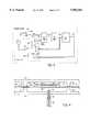
- FIG. 4is a cross sectional view of fixture 15.
- Fixture 15includes first section 14, second section 16, and an antenna in each enclosure (or cavity). For example, cavities 71, 72 and 74 are shown with antenna 66 in cavity 72.
- First section 14includes a matrix of ridges, for example 52 and 56.
- Second section 16includes a matching matrix of ridges, for example 54 and 58. Each pair of ridges for example 56 and 58 separates and defines adjacent cavities, for example cavities 72 and 74.
- the upper surface of ridges 54 and 58 in second section 16define a horizontal plane onto which a portion of roll 20 of laminated films is positioned.
- material handling apparatusposition the portion for in-sheet transponder testing.
- First section 14 and second section 16are then pressed together against sheet 20 so that each transponder, for example transponder 51, is isolated from each other transponder in sheet 20. Ridges about each cavity form an RF seal.
- the RF sealprovides isolation. Isolation prevents RF energy radiated from antenna 66 in cavity 72 from interfering with tests conducted in adjacent cavity 74.
- the RF sealis not perfect and, therefore, isolation is not perfect, due to leakage for example between ridges 52 and 54 and between 56 and 58. Since leakage RF energy must pass through films 44 and 46, conventional shielding in the neighborhood of the contact between adjacent ridges is effective to further reduce leakage and thereby improve isolation. Such shielding includes placement of conductors and conductive materials within, between, and on the surfaces of films 44 and 46.
- Isolationis operative to decouple an antenna in one enclosure from an antenna in an adjacent enclosure. From the point of view at antenna 66, when a signal originating in cavity 72 is stronger than a signal originating in cavity 74, for example, the signal sources and their respective antennas are considered decoupled from each other. Decoupling can also be accomplished by improving the gain of cavity 72, for example, by making its dimensions compatible with a wavelength of the signal originating in cavity 72.
- first section 14 and second section 16are fabricated as flat plates having no ridges 52, 54, 56, or 58. The distance between these plates is smaller than one wavelength of the signal originating in cavity 72 so that adjacent transponder antennas are effectively decoupled for purposes including manufacturing acceptance testing. In such an embodiment, first section 14 and second section 16 sandwich the sheet therebetween.
- each transponderis formed within a square contour and each cavity has a matching square cross section so that transponders are isolated each one at its contour.
- a contourextends through both films 44 and 46 to circumscribe one transponder.
- a contouris defined on a surface. Since top film 44 has an upper surface, a first contour is defined on that top surface. Since bottom film 46 has a bottom surface, a second contour is defined on that bottom surface.
- the square cavity formed by ridges 54 and 58 in the second sectionis circumscribed by a third contour in the plane defined by the tops of the ridges on which the sheet is positioned.
- alignmentincludes positioning the sheet and the fixture so that the third contour formed on ridges 54 and 58 touches the sheet at the second contour on the bottom of film 46.
- the first sectionhaving a similar fourth contour on ridges 52 and 56, touches the first contour on the top of film 44.
- the first and second contoursare directly opposed through the sheet.
- ridges 52 and 54touch film 44 along a sloped, concave, notched, or stepped surface for greater isolation. In such embodiments, important contours are not necessarily directly opposed.
- Transponder 51is identical to transponder 12 as previously described. Transponder 51 is of the type described as an enclosed transceiver in U.S. patent application Ser. No. 08/123,030, filed Sep. 14, 1993, incorporated herein by reference.
- the cross-sectional view of transponder 51shows integrated circuit 48 and battery 50 between film 44 and film 46.
- Integrated circuit 48includes the transceiver circuitry of transponder 51.
- Battery 50in one embodiment, includes a metal surface coupled to operate as part of the antenna for the transceiver circuitry. Additional conductive traces on film 44 and film 46 cooperate for coupling battery power to integrated circuit 48 and for operation as part of the antenna for the transceiver.
- Films 44 and 46are sealed to each other around a contour that encircles integrated circuit 48 and battery 50.
- the sealis made by embossing so that the thickness of films 44 and 46 is reduced as shown at seal 42.
- transceiver 51is separated from the sheet by cutting through films 44 and 46 at a point outside seal 42 so that transceiver 51 remains sealed after testing.
- the central internal conductor of coax cable 70is extended into cavity 72 for operation as a near-field antenna.
- Feed through fitting 68holds coax cable 70 onto second section 16, shields the central conductor, and provides continuity of impedance from cable 70 up to antenna 66.
- the amount of radiation coupled between antenna 66 and transponder 51depends in part on several variables including the dimensions of cavity 72, the wavelengths of the radiated signals, potting or other materials (if any) within the enclosure, and the distance between antenna 66 and film 46. Although the location of transponder 51 is controlled by maintaining tension on sheet 20 as first section 14 is pressed against second section 16, these variables are expected to vary to some extent from cavity to cavity, from test to test, and over time with wear and handling of fixture 15 and operation and wear in materials handling apparatus used to position fixture 15, sheet 20, or both.
- antenna 110 of transponder 12is a square loop antenna for communication at about 2.45 gigahertz.
- the wavelength at that frequencyis about 12.2 centimeters or about 4.82 inches.
- cavity dimensions discussed abovemust lie outside the loop antenna. Conventional simulation may be used to arrive at sufficient or optimal dimensions of the cavity and sufficient or optimal dimensional characteristics of the antenna, including its placement and type (dipole, loop, stub, Marconi, etc).
- the magnitude of signal 117 as shown in FIG. 3is determined so that the effect of variation in the variables discussed above is removed from transponder test results and the pass rate for tested transponders is improved.
- Such a methodbegins with a first step of characterizing the encapsulated transponder with far-field tests. Before transponder 51 is tested in fixture 15, the digitization transfer function for analog to digital converter 124 shown in FIG. 3 is determined in a second step. As with the first step, in this second step, a desired level of accuracy for manufacturing acceptance tests is achieved using one of several approaches including design simulation, theoretical analysis, tests of a prototype, tests of representative samples, or tests of every transponder. In a preferred embodiment, sufficient accuracy is obtained for a manufacturing lot of transponders by conducting wafer probe tests for the second step.
- the cavityis characterized by design simulation, theoretical analysis, or conventional tests.
- a prototype or representative transponder 51is placed in the cavity shown in FIG. 4 that was characterized in the third step.
- a pass/fail test power level and the expected reported signal strengthare determined by analysis of the results of tests made with the representative transponder, the characterization data, and the results of simulation and other techniques known in the art. Together the process of determining in this fifth step is defined as correlating far-field measurements with transceiver responses.
- manufacturing acceptance testingcan proceed by replacing the representative transponder with an untested transponder 51. While in the cavity and isolated from other transponders, several tests are performed including a receiver sensitivity test.
- a receiver sensitivity test of the present inventionincludes the following steps: radiating a test signal from antenna 66; converting analog signal RSS1 received by antenna 110 to a digital result on line 125; transmitting, by means of transmitter 128 and antenna 110, a message conveying the digital result; receiving the message via antenna 66; and making a pass/fail determination based on the response (if any) from the untested transponder. As one result, defects in antenna 110, switch 112, and receiver circuit 118 are made apparent.
- the orientation and shape of fixture 15 as two plates as shown in FIGS. 1 and 4 in alternate and equivalent embodimentsare modified for cooperation with material handling apparatus, not shown.
- the plane at which first section 14 and second section 16 meetis vertical rather than horizontal.
- the fixturehas a spherical shape (rather than generally hexahedral), each contour surrounding a transponder is circular (rather than square), and each cavity is spherical (rather than generally hexahedral).
- antenna 66is located in various positions including, for example, in an opposite section of a cavity, within a ridge, in an adjoining cavity not completely isolated by ridges, or (for multiple antennas per cavity) at several of these locations.
- first section 14, second section 16, or both in alternate and equivalent embodimentsare formed along an axis of turning to permit advancing a portion of sheet 20 as a portion of the fixture turns about its axis. In one embodiment, such movement moves and aligns sheet 20.
- a microwave frequency bandis used for transponder communication.
- the same bandis used for transponder testing.
- another one or more frequency bandsare utilized.
- transponder 12 shown in FIG. 3in alternate embodiments is simplified.
- transmitter 128is replaced with a transmitter responsive to an analog instead of a digital input
- receiver circuit 118is replaced with a circuit providing an analog rather than a digital output
- analog to digital converter 124is eliminated and CPU 126 is replaced with an analog rather than a digital circuit.
- a "system”refers generally to electrical apparatus and includes but is not limited to rack and panel instrumentation, a packaged integrated circuit, an unpackaged integrated circuit, a combination of packaged or unpackaged integrated circuits or both, a microprocessor, a microcontroller, a memory, a register, a flip-flop, a charge-coupled device, combinations thereof, and equivalents.
- a “signal”refers to mechanical and/or electromagnetic energy conveying information. When elements are coupled, a signal is conveyed in any manner feasible with regard to the nature of the coupling. For example, if several electrical conductors couple two elements, then the relevant signal comprises the energy on one, some, or all conductors at a given time or time period.
- a physical property of a signalhas a quantitative measure and the property is used by design to control or communicate information, then the signal is said to be characterized by having a "magnitude" or "value.” The measure may be instantaneous or an average.
Landscapes
- Engineering & Computer Science (AREA)
- Physics & Mathematics (AREA)
- General Physics & Mathematics (AREA)
- Computer Hardware Design (AREA)
- Microelectronics & Electronic Packaging (AREA)
- General Engineering & Computer Science (AREA)
- Theoretical Computer Science (AREA)
- Artificial Intelligence (AREA)
- Computer Vision & Pattern Recognition (AREA)
- Computer Networks & Wireless Communication (AREA)
- Near-Field Transmission Systems (AREA)
- Radar Systems Or Details Thereof (AREA)
Abstract
Description
Claims (5)
Priority Applications (6)
| Application Number | Priority Date | Filing Date | Title |
|---|---|---|---|
| US08/306,906US5983363A (en) | 1992-11-20 | 1994-09-15 | In-sheet transceiver testing |
| US09/437,718US6487681B1 (en) | 1992-11-20 | 1999-11-09 | In-sheet transceiver testing |
| US10/997,556USRE42872E1 (en) | 1992-11-20 | 2004-11-24 | Method and apparatus for communicating with RFID devices coupled to a roll of flexible material |
| US11/864,708USRE43935E1 (en) | 1992-11-20 | 2007-09-28 | Method and apparatus for RFID communication |
| US11/864,715USRE43940E1 (en) | 1992-11-20 | 2007-09-28 | Method and apparatus for RFID communication |
| US11/864,718USRE43918E1 (en) | 1992-11-20 | 2007-09-28 | Method and apparatus for RFID communication |
Applications Claiming Priority (2)
| Application Number | Priority Date | Filing Date | Title |
|---|---|---|---|
| US07/979,607US6058497A (en) | 1992-11-20 | 1992-11-20 | Testing and burn-in of IC chips using radio frequency transmission |
| US08/306,906US5983363A (en) | 1992-11-20 | 1994-09-15 | In-sheet transceiver testing |
Related Parent Applications (1)
| Application Number | Title | Priority Date | Filing Date |
|---|---|---|---|
| US07/979,607Continuation-In-PartUS6058497A (en) | 1992-11-20 | 1992-11-20 | Testing and burn-in of IC chips using radio frequency transmission |
Related Child Applications (2)
| Application Number | Title | Priority Date | Filing Date |
|---|---|---|---|
| US09/437,718ContinuationUS6487681B1 (en) | 1992-11-20 | 1999-11-09 | In-sheet transceiver testing |
| US10/997,556ContinuationUSRE42872E1 (en) | 1992-11-20 | 2004-11-24 | Method and apparatus for communicating with RFID devices coupled to a roll of flexible material |
Publications (1)
| Publication Number | Publication Date |
|---|---|
| US5983363Atrue US5983363A (en) | 1999-11-09 |
Family
ID=26975426
Family Applications (6)
| Application Number | Title | Priority Date | Filing Date |
|---|---|---|---|
| US08/306,906Expired - LifetimeUS5983363A (en) | 1992-11-20 | 1994-09-15 | In-sheet transceiver testing |
| US09/437,718CeasedUS6487681B1 (en) | 1992-11-20 | 1999-11-09 | In-sheet transceiver testing |
| US10/997,556Expired - LifetimeUSRE42872E1 (en) | 1992-11-20 | 2004-11-24 | Method and apparatus for communicating with RFID devices coupled to a roll of flexible material |
| US11/864,715Expired - Fee RelatedUSRE43940E1 (en) | 1992-11-20 | 2007-09-28 | Method and apparatus for RFID communication |
| US11/864,718Expired - LifetimeUSRE43918E1 (en) | 1992-11-20 | 2007-09-28 | Method and apparatus for RFID communication |
| US11/864,708Expired - LifetimeUSRE43935E1 (en) | 1992-11-20 | 2007-09-28 | Method and apparatus for RFID communication |
Family Applications After (5)
| Application Number | Title | Priority Date | Filing Date |
|---|---|---|---|
| US09/437,718CeasedUS6487681B1 (en) | 1992-11-20 | 1999-11-09 | In-sheet transceiver testing |
| US10/997,556Expired - LifetimeUSRE42872E1 (en) | 1992-11-20 | 2004-11-24 | Method and apparatus for communicating with RFID devices coupled to a roll of flexible material |
| US11/864,715Expired - Fee RelatedUSRE43940E1 (en) | 1992-11-20 | 2007-09-28 | Method and apparatus for RFID communication |
| US11/864,718Expired - LifetimeUSRE43918E1 (en) | 1992-11-20 | 2007-09-28 | Method and apparatus for RFID communication |
| US11/864,708Expired - LifetimeUSRE43935E1 (en) | 1992-11-20 | 2007-09-28 | Method and apparatus for RFID communication |
Country Status (1)
| Country | Link |
|---|---|
| US (6) | US5983363A (en) |
Cited By (54)
| Publication number | Priority date | Publication date | Assignee | Title |
|---|---|---|---|---|
| US6259353B1 (en)* | 1997-05-16 | 2001-07-10 | U.S. Philips Corporation | Transponder communication device for the contactless communication with mobile transponders, including means for carrying out an operational test, and transponder constructed as an operational-test transponder |
| WO2002037413A1 (en)* | 2000-10-31 | 2002-05-10 | Koninklijke Philips Electronics N.V. | Data carrier having means for communicating the value of its d.c. supply voltage to a communication station |
| US6412086B1 (en)* | 1998-06-01 | 2002-06-25 | Intermec Ip Corp. | Radio frequency identification transponder integrated circuit having a serially loaded test mode register |
| US6466990B2 (en)* | 1993-12-17 | 2002-10-15 | Storage Technology Corporation | System and method for data storage management |
| WO2002087238A1 (en)* | 2001-04-10 | 2002-10-31 | Fantalife Co., Ltd. | A pc based tv set-top box system and method of providing contents exclusively by the system |
| US6487681B1 (en)* | 1992-11-20 | 2002-11-26 | Micron Technology, Inc. | In-sheet transceiver testing |
| US20030029146A1 (en)* | 2001-08-10 | 2003-02-13 | General Signal Technology | Filter assembly and method with polyimide |
| US20040075607A1 (en)* | 2000-04-26 | 2004-04-22 | Cathey David A. | Automated antenna trim for transmitting and receiving semiconductor devices |
| US6759863B2 (en) | 2000-05-15 | 2004-07-06 | The Governors Of The University Of Alberta | Wireless radio frequency technique design and method for testing of integrated circuits and wafers |
| US20040160233A1 (en)* | 2003-02-13 | 2004-08-19 | Forster Ian J. | RFID device tester and method |
| US6784789B2 (en)* | 1999-07-08 | 2004-08-31 | Intermec Ip Corp. | Method and apparatus for verifying RFID tags |
| US20040195319A1 (en)* | 2003-04-03 | 2004-10-07 | Forster Ian J. | RFID device detection system and method |
| US20050138499A1 (en)* | 2003-11-26 | 2005-06-23 | Lawrence Pileggi | System and method to test integrated circuits on a wafer |
| US20050183817A1 (en)* | 2004-02-23 | 2005-08-25 | Eric Eckstein | Security tag system for fabricating a tag including an integrated surface processing system |
| US20050183264A1 (en)* | 2004-02-23 | 2005-08-25 | Eric Eckstein | Method for aligning capacitor plates in a security tag and a capacitor formed thereby |
| US20050187837A1 (en)* | 2004-02-23 | 2005-08-25 | Eric Eckstein | Method and system for determining billing information in a tag fabrication process |
| US20050184873A1 (en)* | 2004-02-23 | 2005-08-25 | Eric Eckstein | Tag having patterned circuit elements and a process for making same |
| US20060000907A1 (en)* | 2004-07-01 | 2006-01-05 | Forster Ian J | RFID device preparation system and method |
| US20060012387A1 (en)* | 2004-06-29 | 2006-01-19 | Symbol Technologies, Inc. | Systems and methods for testing radio frequency identification tags |
| US20060055542A1 (en)* | 2004-09-13 | 2006-03-16 | Forster Ian J | RFID device with content insensitivity and position insensitivity |
| US20060068711A1 (en)* | 2004-09-16 | 2006-03-30 | Chiu Lihu M | RFID verifier |
| US20060091225A1 (en)* | 2003-11-04 | 2006-05-04 | Forster Ian J | RFID tag using a surface insensitive antenna structure |
| US20060202705A1 (en)* | 2005-03-14 | 2006-09-14 | Forster Ian J | RFID application test systems and methods |
| US20060220858A1 (en)* | 2005-03-29 | 2006-10-05 | Fujitsu Limited | Tag testing device, tag testing method, and tag testing program |
| US20060220859A1 (en)* | 2003-09-19 | 2006-10-05 | Brother Kogyo Kabushiki Kaisha | RFID tag reader/writer |
| US20060226983A1 (en)* | 2005-04-07 | 2006-10-12 | Forster Ian J | RFID device test thresholds systems and methods |
| US20060226864A1 (en)* | 2005-04-06 | 2006-10-12 | Kramer Bradley A | Expeditious and low cost testing of RFID ICs |
| US20060250245A1 (en)* | 2005-05-09 | 2006-11-09 | Forster Ian J | RFID communication systems and methods |
| US20060250246A1 (en)* | 2005-05-09 | 2006-11-09 | Forster Ian J | RFID test interface systems and methods |
| US7138919B2 (en) | 2004-02-23 | 2006-11-21 | Checkpoint Systems, Inc. | Identification marking and method for applying the identification marking to an item |
| US20060271328A1 (en)* | 2005-05-25 | 2006-11-30 | Forster Ian J | RFID device variable test systems and methods |
| US7154283B1 (en) | 2006-02-22 | 2006-12-26 | Avery Dennison Corporation | Method of determining performance of RFID devices |
| US7164353B2 (en) | 2004-12-22 | 2007-01-16 | Avery Dennison Corporation | Method and system for testing RFID devices |
| US20070013522A1 (en)* | 2004-09-16 | 2007-01-18 | Chiu Lihu M | RFID verifier |
| US20070018831A1 (en)* | 2005-07-19 | 2007-01-25 | Smurfit-Stone Container Enterprises, Inc. | Methods and systems for in-line RFID transponder testing |
| US20070039687A1 (en)* | 2005-08-22 | 2007-02-22 | Hamilton Kevin S | Method of making RFID devices |
| US20070273481A1 (en)* | 2006-05-25 | 2007-11-29 | Symbol Technologies, Inc. | RFID tag with programmable read range |
| US20080000074A1 (en)* | 2006-05-05 | 2008-01-03 | Genaro Martinez | Computer automated tag test system |
| US7327264B1 (en) | 2004-09-16 | 2008-02-05 | Storage Technology Corporation | System and method for extending performance of media cartridge RF identification |
| US20080183407A1 (en)* | 2006-12-27 | 2008-07-31 | Industrial Technology Research Institute | System and method for testing power intensify of rfid tags |
| US7411498B2 (en) | 2005-04-07 | 2008-08-12 | Avery Dennison | RFID testing and classification systems and methods |
| US7652636B2 (en) | 2003-04-10 | 2010-01-26 | Avery Dennison Corporation | RFID devices having self-compensating antennas and conductive shields |
| US7704346B2 (en) | 2004-02-23 | 2010-04-27 | Checkpoint Systems, Inc. | Method of fabricating a security tag in an integrated surface processing system |
| US20100115572A1 (en)* | 2008-11-05 | 2010-05-06 | Comcast Cable Communications, Llc | System and method for providing digital content |
| EP1784803A4 (en)* | 2004-08-17 | 2010-07-14 | Symbol Technologies Inc | Singulation of radio frequency identification (rfid) tags for testing and/or programming |
| US20100207729A1 (en)* | 2009-02-13 | 2010-08-19 | Industrial Technology Research Institute | Method and system for testing rfid tags |
| US7808367B2 (en) | 1999-08-09 | 2010-10-05 | Round Rock Research, Llc | RFID material tracking method and apparatus |
| US7884724B2 (en) | 1996-07-30 | 2011-02-08 | Round Rock Research, Llc | Radio frequency data communications device with selectively removable antenna portion and method |
| CN1661387B (en)* | 2004-01-30 | 2011-07-06 | 株式会社半导体能源研究所 | Inspection system, inspection method, and method for manufacturing semiconductor device |
| EP1598767A3 (en)* | 2004-05-20 | 2012-05-02 | Xerox Corporation | Diagnosis of programmable modules |
| WO2012037444A3 (en)* | 2010-09-17 | 2012-05-31 | Cascade Microtech, Inc. | Systems and methods for non-contact power and data transfer in electronic devices |
| WO2012148686A1 (en)* | 2011-04-26 | 2012-11-01 | Avery Dennison Corporation | System and method for automated rfid quality control |
| US10571487B2 (en) | 2016-11-30 | 2020-02-25 | Formfactor Beaverton, Inc. | Contact engines, probe head assemblies, probe systems, and associated methods for on-wafer testing of the wireless operation of a device under test |
| US12306243B2 (en) | 2023-06-12 | 2025-05-20 | Formfactor, Inc. | Space transformers configured to be utilized in a probe system, probe systems that include the space transformers, and related methods |
Families Citing this family (26)
| Publication number | Priority date | Publication date | Assignee | Title |
|---|---|---|---|---|
| US6951596B2 (en) | 2002-01-18 | 2005-10-04 | Avery Dennison Corporation | RFID label technique |
| US7030977B2 (en)* | 2003-05-06 | 2006-04-18 | Visteon Global Technologies, Inc. | Non-contact optical system for production testing of electronic assemblies |
| US20050176376A1 (en)* | 2004-02-11 | 2005-08-11 | Accton Technology Corporation | Batch testing system and method for wireless communication devices |
| US7136683B2 (en)* | 2004-03-23 | 2006-11-14 | Honeywell International Inc. | Surface acoustic wave sensor and radio frequency identification interrogator fixture |
| US7000461B2 (en)* | 2004-03-23 | 2006-02-21 | Honeywell International Inc. | Patch wireless test fixture |
| DE102004049071A1 (en)* | 2004-08-20 | 2006-03-09 | Mühlbauer Ag | Ultra-high frequency test device for transponders |
| US7500307B2 (en) | 2004-09-22 | 2009-03-10 | Avery Dennison Corporation | High-speed RFID circuit placement method |
| US7646284B2 (en)* | 2004-11-17 | 2010-01-12 | Lexmark International, Inc. | Systems and apparatus for writing data to multiple RF tags contained on print media |
| US7712674B1 (en)* | 2005-02-22 | 2010-05-11 | Eigent Technologies Llc | RFID devices for verification of correctness, reliability, functionality and security |
| US7623034B2 (en) | 2005-04-25 | 2009-11-24 | Avery Dennison Corporation | High-speed RFID circuit placement method and device |
| US7301458B2 (en)* | 2005-05-11 | 2007-11-27 | Alien Technology Corporation | Method and apparatus for testing RFID devices |
| US7309007B2 (en)* | 2005-10-04 | 2007-12-18 | First Data Corporation | Systems and methods for personalizing transaction cards |
| DE102005048872A1 (en)* | 2005-10-12 | 2007-04-26 | Mühlbauer Ag | Test head device |
| US7555826B2 (en) | 2005-12-22 | 2009-07-07 | Avery Dennison Corporation | Method of manufacturing RFID devices |
| DE102006022160B3 (en)* | 2006-05-12 | 2007-12-27 | Mühlbauer Ag | Test device with HF / UHF dual band antenna for testing RFID transponders in a production device |
| US7486889B2 (en)* | 2006-06-23 | 2009-02-03 | International Business Machines Corporation | Transceiver test module employing an optical wrap |
| DE102006040180A1 (en)* | 2006-08-26 | 2008-03-13 | Nordenia Deutschland Gronau Gmbh | Method for contactless testing of webs mounted on a web |
| US20080100329A1 (en)* | 2006-10-31 | 2008-05-01 | Symbol Technologies, Inc. | System and method for multi-up inline testing of radio frequency identification (RFID) inlays |
| DE102007006274A1 (en)* | 2007-02-08 | 2008-08-14 | Polyic Gmbh & Co. Kg | Measuring device with a measuring wheel |
| JP2018041472A (en) | 2012-08-30 | 2018-03-15 | セイコーエプソン株式会社 | Medium processing apparatus and medium processing method |
| JP6221370B2 (en)* | 2012-08-30 | 2017-11-01 | セイコーエプソン株式会社 | Medium processing apparatus and method for controlling medium processing apparatus |
| US9195864B2 (en) | 2013-02-18 | 2015-11-24 | Lawrence D. Simmons, JR. | Geographic chip locator |
| JP6378909B2 (en)* | 2014-03-19 | 2018-08-22 | サトーホールディングス株式会社 | RFID medium read / write verification apparatus and read / write verification method thereof |
| US9729201B2 (en)* | 2014-04-24 | 2017-08-08 | Empire Technology Development Llc | Broadcasting a message using modulated power |
| JP2017044498A (en)* | 2015-08-24 | 2017-03-02 | 大日本印刷株式会社 | Frequency measuring method, frequency measuring device, frequency measuring jig |
| US9806828B2 (en) | 2016-02-24 | 2017-10-31 | Frontier Engineering, Llc | Radio frequency generator automated test system |
Citations (14)
| Publication number | Priority date | Publication date | Assignee | Title |
|---|---|---|---|---|
| US4704734A (en)* | 1986-02-18 | 1987-11-03 | Motorola, Inc. | Method and apparatus for signal strength measurement and antenna selection in cellular radiotelephone systems |
| US4996715A (en)* | 1987-09-29 | 1991-02-26 | Kabushiki Kaisha Toshiba | Radio telephone apparatus |
| US5068521A (en)* | 1989-05-18 | 1991-11-26 | Mitsubishi Denki Kabushiki Kaisha | Non-contact ic card |
| US5087920A (en)* | 1987-07-30 | 1992-02-11 | Sony Corporation | Microwave antenna |
| US5113184A (en)* | 1987-09-22 | 1992-05-12 | Hitachi Maxell, Ltd. | Method and system of communication for a non-contact ic card |
| US5149662A (en)* | 1991-03-27 | 1992-09-22 | Integrated System Assemblies Corporation | Methods for testing and burn-in of integrated circuit chips |
| US5198647A (en)* | 1989-11-28 | 1993-03-30 | Mitsubishi Denki Kabushiki Kaisha | Plural-coil non-contact ic card having pot cores and shielding walls |
| US5212373A (en)* | 1990-07-03 | 1993-05-18 | Mitsubishi Denki Kabushiki Kaisha | Non-contact ic card |
| US5252914A (en)* | 1990-08-06 | 1993-10-12 | Ericsson Ge Mobile Communications Inc. | Method of constructing and testing a circuit board designed for early diagnostics |
| US5279975A (en)* | 1992-02-07 | 1994-01-18 | Micron Technology, Inc. | Method of testing individual dies on semiconductor wafers prior to singulation |
| US5315241A (en)* | 1991-09-18 | 1994-05-24 | Sgs-Thomson Microelectronics, Inc. | Method for testing integrated circuits |
| US5349139A (en)* | 1992-10-30 | 1994-09-20 | International Business Machines | Architecture for communication of remote devices to a digitizing display |
| US5434394A (en)* | 1992-09-10 | 1995-07-18 | Tandy Corporation | Automated order and delivery system |
| US5455575A (en)* | 1992-11-06 | 1995-10-03 | Texas Instruments Deutschland Gmbh | Multi-interrogator, datacom and transponder arrangement |
Family Cites Families (68)
| Publication number | Priority date | Publication date | Assignee | Title |
|---|---|---|---|---|
| US3713148A (en)* | 1970-05-21 | 1973-01-23 | Communications Services Corp I | Transponder apparatus and system |
| US3679874A (en) | 1970-07-06 | 1972-07-25 | Bendix Corp | Automatic baggage handling system |
| US3689885A (en) | 1970-09-15 | 1972-09-05 | Transitag Corp | Inductively coupled passive responder and interrogator unit having multidimension electromagnetic field capabilities |
| JPS547196B2 (en) | 1971-08-26 | 1979-04-04 | ||
| US4384288A (en)* | 1980-12-31 | 1983-05-17 | Walton Charles A | Portable radio frequency emitting identifier |
| DK291184D0 (en) | 1984-06-13 | 1984-06-13 | Boeegh Petersen Allan | METHOD AND DEVICE FOR TESTING CIRCUIT PLATES |
| US4761778A (en) | 1985-04-11 | 1988-08-02 | Massachusetts Institute Of Technology | Coder-packetizer for random accessing in digital communication with multiple accessing |
| US4776464A (en) | 1985-06-17 | 1988-10-11 | Bae Automated Systems, Inc. | Automated article handling system and process |
| US5008661A (en) | 1985-09-27 | 1991-04-16 | Raj Phani K | Electronic remote chemical identification system |
| US4704614A (en)* | 1985-11-06 | 1987-11-03 | The United States Of America As Represented By The Secretary Of The Air Force | Apparatus for scanning and measuring the near-field radiation of an antenna |
| US4850009A (en) | 1986-05-12 | 1989-07-18 | Clinicom Incorporated | Portable handheld terminal including optical bar code reader and electromagnetic transceiver means for interactive wireless communication with a base communications station |
| US4750197A (en) | 1986-11-10 | 1988-06-07 | Denekamp Mark L | Integrated cargo security system |
| JP2514954B2 (en) | 1987-03-13 | 1996-07-10 | 三菱電機株式会社 | IC card |
| JPH01123269U (en) | 1988-02-16 | 1989-08-22 | ||
| US4860602A (en)* | 1988-05-18 | 1989-08-29 | Harris Corporation | RF transparent thermal test chamber |
| AU626013B2 (en) | 1988-07-04 | 1992-07-23 | Sony Corporation | A thin electronic device having an integrated circuit chip and a power battery and a method for producing same |
| US4999636A (en) | 1989-02-17 | 1991-03-12 | Amtech Technology Corporation | Range limiting system |
| US5153524A (en)* | 1989-03-29 | 1992-10-06 | The United States Of America As Represented By The Secretary Of The Army | Testing electromagnetic shielding effectiveness of shielded enclosures |
| JP3087294B2 (en) | 1989-09-29 | 2000-09-11 | ジェイエスアール株式会社 | Method for producing anisotropic conductive sheet |
| SE464946B (en) | 1989-11-10 | 1991-07-01 | Philips Norden Ab | TRANSMISSION SYSTEM INCLUDING A QUESTION STATION AND NUMBER OF ANSWERING STATIONS |
| JPH0772907B2 (en) | 1989-12-21 | 1995-08-02 | 三菱電機株式会社 | Microcomputer and non-contact IC card using the same |
| JP2535084B2 (en) | 1990-02-19 | 1996-09-18 | シャープ株式会社 | Method for manufacturing semiconductor device |
| JP2645163B2 (en) | 1990-03-13 | 1997-08-25 | 三菱電機株式会社 | Non-contact IC card |
| JP2527267B2 (en) | 1990-04-19 | 1996-08-21 | 三菱電機株式会社 | Non-contact type portable carrier |
| US5347274A (en) | 1990-05-17 | 1994-09-13 | At/Comm Incorporated | Hazardous waste transport management system |
| US5148618A (en) | 1990-06-01 | 1992-09-22 | Brewster Blair M | Sealed tag |
| US5274221A (en) | 1990-06-22 | 1993-12-28 | Mitsubishi Denki Kabushiki Kaisha | Non-contact integrated circuit card |
| JP2608167B2 (en) | 1990-08-21 | 1997-05-07 | 三菱電機株式会社 | IC tester |
| US5219765A (en) | 1990-09-12 | 1993-06-15 | Hitachi, Ltd. | Method for manufacturing a semiconductor device including wafer aging, probe inspection, and feeding back the results of the inspection to the device fabrication process |
| JP2549192B2 (en) | 1990-09-19 | 1996-10-30 | 三菱電機株式会社 | Non-contact IC card and method of using the same |
| US5121407A (en) | 1990-09-27 | 1992-06-09 | Pittway Corporation | Spread spectrum communications system |
| US5148103A (en) | 1990-10-31 | 1992-09-15 | Hughes Aircraft Company | Apparatus for testing integrated circuits |
| US5340968A (en) | 1991-05-07 | 1994-08-23 | Nippondenso Company, Ltd. | Information storage medium with electronic and visual areas |
| US5266925A (en) | 1991-09-30 | 1993-11-30 | Westinghouse Electric Corp. | Electronic identification tag interrogation method |
| US5278571A (en)* | 1991-10-16 | 1994-01-11 | Tel Instrument Electronics Corp. | RF coupler for measuring RF parameters in the near-field |
| US5343478A (en) | 1991-11-27 | 1994-08-30 | Ncr Corporation | Computer system configuration via test bus |
| US5247577A (en)* | 1992-05-13 | 1993-09-21 | Intel Corporation | Methods and apparatus for securely enabling features in highly integrated electronic circuits |
| US5365551A (en)* | 1992-12-15 | 1994-11-15 | Micron Technology, Inc. | Data communication transceiver using identification protocol |
| US5801432A (en) | 1992-06-04 | 1998-09-01 | Lsi Logic Corporation | Electronic system using multi-layer tab tape semiconductor device having distinct signal, power and ground planes |
| US5776278A (en)* | 1992-06-17 | 1998-07-07 | Micron Communications, Inc. | Method of manufacturing an enclosed transceiver |
| DE4345610B4 (en) | 1992-06-17 | 2013-01-03 | Micron Technology Inc. | Method for producing a radio-frequency identification device (HFID) |
| US6045652A (en) | 1992-06-17 | 2000-04-04 | Micron Communications, Inc. | Method of manufacturing an enclosed transceiver |
| US7158031B2 (en)* | 1992-08-12 | 2007-01-02 | Micron Technology, Inc. | Thin, flexible, RFID label and system for use |
| US5983363A (en)* | 1992-11-20 | 1999-11-09 | Micron Communications, Inc. | In-sheet transceiver testing |
| US6058497A (en) | 1992-11-20 | 2000-05-02 | Micron Technology, Inc. | Testing and burn-in of IC chips using radio frequency transmission |
| US5373503A (en) | 1993-04-30 | 1994-12-13 | Information Technology, Inc. | Group randomly addressed polling method |
| DE4323883C2 (en) | 1993-07-16 | 2002-11-07 | Meto International Gmbh | Theft security tag |
| KR0140034B1 (en) | 1993-12-16 | 1998-07-15 | 모리시다 요이치 | Semiconductor wafer storage device, connection method between integrated circuit terminal and probe terminal for inspection of semiconductor wafer and apparatus therefor, inspection method for semiconductor integrated circuit, probe card and manufacturing method thereof |
| US5751256A (en) | 1994-03-04 | 1998-05-12 | Flexcon Company Inc. | Resonant tag labels and method of making same |
| US5521600A (en) | 1994-09-06 | 1996-05-28 | The Regents Of The University Of California | Range-gated field disturbance sensor with range-sensitivity compensation |
| US5672981A (en) | 1994-09-16 | 1997-09-30 | At&T Global Information Solutions Company | Universal power interface adapter for burn-in board |
| JP3185576B2 (en) | 1994-12-22 | 2001-07-11 | 株式会社デンソー | Vehicle communication device |
| US5671362A (en) | 1995-04-04 | 1997-09-23 | Cowe; Alan B. | Materials monitoring systems, materials management systems and related methods |
| US5798693A (en) | 1995-06-07 | 1998-08-25 | Engellenner; Thomas J. | Electronic locating systems |
| US5785181A (en) | 1995-11-02 | 1998-07-28 | Clothestrak, Inc. | Permanent RFID garment tracking system |
| EP0776063A1 (en) | 1995-11-27 | 1997-05-28 | Nippon Paint Co., Ltd. | Electromagnetic wave absorbing and shielding |
| US5828693A (en) | 1996-03-21 | 1998-10-27 | Amtech Corporation | Spread spectrum frequency hopping reader system |
| US5887176A (en) | 1996-06-28 | 1999-03-23 | Randtec, Inc. | Method and system for remote monitoring and tracking of inventory |
| EP0953181B8 (en) | 1997-01-17 | 2005-10-05 | Tagsys SA | Multiple tag reading system |
| US5920287A (en) | 1997-01-21 | 1999-07-06 | Widata Corporation | Radio location system for precisely tracking objects by RF transceiver tags which randomly and repetitively emit wideband identification signals |
| US5949246A (en) | 1997-01-28 | 1999-09-07 | International Business Machines | Test head for applying signals in a burn-in test of an integrated circuit |
| US6144301A (en) | 1997-02-10 | 2000-11-07 | Safetrac Control Systems, Inc. | Electronic tracking tag |
| US5764655A (en) | 1997-07-02 | 1998-06-09 | International Business Machines Corporation | Built in self test with memory |
| US6121544A (en) | 1998-01-15 | 2000-09-19 | Petsinger; Julie Ann | Electromagnetic shield to prevent surreptitious access to contactless smartcards |
| DE60143161D1 (en) | 2000-05-03 | 2010-11-11 | Gemalto Sa | A CHIP CARD AND A HOUSING TO THIS |
| US7163152B2 (en) | 2004-12-15 | 2007-01-16 | Osborn Warren R | Protective container for readable cards |
| US20060187060A1 (en) | 2005-02-07 | 2006-08-24 | Colby Steven M | Identity devices including radio frequency shielding |
| US7482925B2 (en) | 2005-06-24 | 2009-01-27 | Visa U.S.A. | Apparatus and method to electromagnetically shield portable consumer devices |
- 1994
- 1994-09-15USUS08/306,906patent/US5983363A/ennot_activeExpired - Lifetime
- 1999
- 1999-11-09USUS09/437,718patent/US6487681B1/ennot_activeCeased
- 2004
- 2004-11-24USUS10/997,556patent/USRE42872E1/ennot_activeExpired - Lifetime
- 2007
- 2007-09-28USUS11/864,715patent/USRE43940E1/ennot_activeExpired - Fee Related
- 2007-09-28USUS11/864,718patent/USRE43918E1/ennot_activeExpired - Lifetime
- 2007-09-28USUS11/864,708patent/USRE43935E1/ennot_activeExpired - Lifetime
Patent Citations (14)
| Publication number | Priority date | Publication date | Assignee | Title |
|---|---|---|---|---|
| US4704734A (en)* | 1986-02-18 | 1987-11-03 | Motorola, Inc. | Method and apparatus for signal strength measurement and antenna selection in cellular radiotelephone systems |
| US5087920A (en)* | 1987-07-30 | 1992-02-11 | Sony Corporation | Microwave antenna |
| US5113184A (en)* | 1987-09-22 | 1992-05-12 | Hitachi Maxell, Ltd. | Method and system of communication for a non-contact ic card |
| US4996715A (en)* | 1987-09-29 | 1991-02-26 | Kabushiki Kaisha Toshiba | Radio telephone apparatus |
| US5068521A (en)* | 1989-05-18 | 1991-11-26 | Mitsubishi Denki Kabushiki Kaisha | Non-contact ic card |
| US5198647A (en)* | 1989-11-28 | 1993-03-30 | Mitsubishi Denki Kabushiki Kaisha | Plural-coil non-contact ic card having pot cores and shielding walls |
| US5212373A (en)* | 1990-07-03 | 1993-05-18 | Mitsubishi Denki Kabushiki Kaisha | Non-contact ic card |
| US5252914A (en)* | 1990-08-06 | 1993-10-12 | Ericsson Ge Mobile Communications Inc. | Method of constructing and testing a circuit board designed for early diagnostics |
| US5149662A (en)* | 1991-03-27 | 1992-09-22 | Integrated System Assemblies Corporation | Methods for testing and burn-in of integrated circuit chips |
| US5315241A (en)* | 1991-09-18 | 1994-05-24 | Sgs-Thomson Microelectronics, Inc. | Method for testing integrated circuits |
| US5279975A (en)* | 1992-02-07 | 1994-01-18 | Micron Technology, Inc. | Method of testing individual dies on semiconductor wafers prior to singulation |
| US5434394A (en)* | 1992-09-10 | 1995-07-18 | Tandy Corporation | Automated order and delivery system |
| US5349139A (en)* | 1992-10-30 | 1994-09-20 | International Business Machines | Architecture for communication of remote devices to a digitizing display |
| US5455575A (en)* | 1992-11-06 | 1995-10-03 | Texas Instruments Deutschland Gmbh | Multi-interrogator, datacom and transponder arrangement |
Cited By (113)
| Publication number | Priority date | Publication date | Assignee | Title |
|---|---|---|---|---|
| US6487681B1 (en)* | 1992-11-20 | 2002-11-26 | Micron Technology, Inc. | In-sheet transceiver testing |
| USRE43935E1 (en)* | 1992-11-20 | 2013-01-15 | Round Rock Research, Llc | Method and apparatus for RFID communication |
| USRE42872E1 (en)* | 1992-11-20 | 2011-10-25 | Round Rock Research, Llc | Method and apparatus for communicating with RFID devices coupled to a roll of flexible material |
| USRE43918E1 (en)* | 1992-11-20 | 2013-01-08 | Round Rock Research, Llc | Method and apparatus for RFID communication |
| USRE43940E1 (en)* | 1992-11-20 | 2013-01-22 | Round Rock Research, Llc | Method and apparatus for RFID communication |
| US6466990B2 (en)* | 1993-12-17 | 2002-10-15 | Storage Technology Corporation | System and method for data storage management |
| US8624711B2 (en) | 1996-07-30 | 2014-01-07 | Round Rock Research, Llc | Radio frequency identification device operating methods, radio frequency identification device configuration methods, and radio frequency identification devices |
| US7884724B2 (en) | 1996-07-30 | 2011-02-08 | Round Rock Research, Llc | Radio frequency data communications device with selectively removable antenna portion and method |
| US6259353B1 (en)* | 1997-05-16 | 2001-07-10 | U.S. Philips Corporation | Transponder communication device for the contactless communication with mobile transponders, including means for carrying out an operational test, and transponder constructed as an operational-test transponder |
| US6412086B1 (en)* | 1998-06-01 | 2002-06-25 | Intermec Ip Corp. | Radio frequency identification transponder integrated circuit having a serially loaded test mode register |
| US6784789B2 (en)* | 1999-07-08 | 2004-08-31 | Intermec Ip Corp. | Method and apparatus for verifying RFID tags |
| US8269605B2 (en) | 1999-08-09 | 2012-09-18 | Round Rock Research, Llc | RFID material tracking method and apparatus |
| US8125316B2 (en) | 1999-08-09 | 2012-02-28 | Round Rock Research, Llc | RFID material tracking method and apparatus |
| US8378789B2 (en) | 1999-08-09 | 2013-02-19 | Round Rock Research, Llc | RFID material tracking method and apparatus |
| US7808367B2 (en) | 1999-08-09 | 2010-10-05 | Round Rock Research, Llc | RFID material tracking method and apparatus |
| US20050062607A1 (en)* | 2000-04-26 | 2005-03-24 | Cathey David A. | Automated antenna trim for transmitting and receiving semiconductor devices |
| US20040075607A1 (en)* | 2000-04-26 | 2004-04-22 | Cathey David A. | Automated antenna trim for transmitting and receiving semiconductor devices |
| US8134467B2 (en) | 2000-04-26 | 2012-03-13 | Round Rock Research, Llc | Automated antenna trim for transmitting and receiving semiconductor devices |
| US6806812B1 (en) | 2000-04-26 | 2004-10-19 | Micron Technology, Inc. | Automated antenna trim for transmitting and receiving semiconductor devices |
| US20070290861A1 (en)* | 2000-04-26 | 2007-12-20 | Micron Technology, Inc. | Automated antenna trim for transmitting and receiving semiconductor devices |
| US7812728B2 (en) | 2000-04-26 | 2010-10-12 | Round Rock Research, Llc | Methods and apparatuses for radio frequency identification (RFID) tags configured to allow antenna trim |
| US7253737B2 (en) | 2000-04-26 | 2007-08-07 | Micron Technology, Inc. | Automated antenna trim for transmitting and receiving semiconductor devices |
| US7417549B2 (en) | 2000-04-26 | 2008-08-26 | Keystone Technology Solutions, Llc | Automated antenna trim for transmitting and receiving semiconductor devices |
| US20040164760A1 (en)* | 2000-05-15 | 2004-08-26 | The Governors Of The University Of Alberta | Wireless radio frequency technique design and method for testing |
| US7183788B2 (en) | 2000-05-15 | 2007-02-27 | Scanimetrics Inc. | Wireless radio frequency technique design and method for testing of integrated circuits and wafers |
| US8028208B2 (en) | 2000-05-15 | 2011-09-27 | Scanimetrics Inc. | Wireless radio frequency technique design and method for testing of integrated circuits and wafers |
| US20070162801A1 (en)* | 2000-05-15 | 2007-07-12 | Brian Moore | Wireless radio frequency technique design and method for testing of integrated circuits and wafers |
| US6759863B2 (en) | 2000-05-15 | 2004-07-06 | The Governors Of The University Of Alberta | Wireless radio frequency technique design and method for testing of integrated circuits and wafers |
| WO2002037413A1 (en)* | 2000-10-31 | 2002-05-10 | Koninklijke Philips Electronics N.V. | Data carrier having means for communicating the value of its d.c. supply voltage to a communication station |
| GB2392573A (en)* | 2001-04-10 | 2004-03-03 | Fantalife Co Ltd | A pc based tv set-top box system and method of providing contents exclusively by the system |
| GB2392573B (en)* | 2001-04-10 | 2005-06-01 | Fantalife Co Ltd | A pc based tv set-top box system and method of providing contents exclusively by the system |
| WO2002087238A1 (en)* | 2001-04-10 | 2002-10-31 | Fantalife Co., Ltd. | A pc based tv set-top box system and method of providing contents exclusively by the system |
| US6833017B2 (en)* | 2001-08-10 | 2004-12-21 | Spx Corporation | Filter assembly and method with polyimide |
| US20030029146A1 (en)* | 2001-08-10 | 2003-02-13 | General Signal Technology | Filter assembly and method with polyimide |
| US7225992B2 (en) | 2003-02-13 | 2007-06-05 | Avery Dennison Corporation | RFID device tester and method |
| US7306162B2 (en) | 2003-02-13 | 2007-12-11 | Avery Dennison Corporation | RFID device tester and method |
| US20050223286A1 (en)* | 2003-02-13 | 2005-10-06 | Forster Ian J | RFID device tester and method |
| US20040160233A1 (en)* | 2003-02-13 | 2004-08-19 | Forster Ian J. | RFID device tester and method |
| US20040195319A1 (en)* | 2003-04-03 | 2004-10-07 | Forster Ian J. | RFID device detection system and method |
| US20060192002A1 (en)* | 2003-04-03 | 2006-08-31 | Forster Ian J | RFID device detection system and method |
| US7059518B2 (en) | 2003-04-03 | 2006-06-13 | Avery Dennison Corporation | RFID device detection system and method |
| US7273173B2 (en) | 2003-04-03 | 2007-09-25 | Avery Dennison Corporation | RFID device detection system and method |
| US7652636B2 (en) | 2003-04-10 | 2010-01-26 | Avery Dennison Corporation | RFID devices having self-compensating antennas and conductive shields |
| US20070080233A1 (en)* | 2003-04-10 | 2007-04-12 | Forster Ian J | RFID tag using a surface insensitive antenna structure |
| US7379024B2 (en) | 2003-04-10 | 2008-05-27 | Avery Dennison Corporation | RFID tag using a surface insensitive antenna structure |
| US8111137B2 (en)* | 2003-09-19 | 2012-02-07 | Brother Kogyo Kabushiki Kaisha | RFID tag reader/writer |
| US20060220859A1 (en)* | 2003-09-19 | 2006-10-05 | Brother Kogyo Kabushiki Kaisha | RFID tag reader/writer |
| US7501984B2 (en) | 2003-11-04 | 2009-03-10 | Avery Dennison Corporation | RFID tag using a surface insensitive antenna structure |
| US20060091225A1 (en)* | 2003-11-04 | 2006-05-04 | Forster Ian J | RFID tag using a surface insensitive antenna structure |
| US20050138499A1 (en)* | 2003-11-26 | 2005-06-23 | Lawrence Pileggi | System and method to test integrated circuits on a wafer |
| US7325180B2 (en)* | 2003-11-26 | 2008-01-29 | Carnegie Mellon University | System and method to test integrated circuits on a wafer |
| CN1661387B (en)* | 2004-01-30 | 2011-07-06 | 株式会社半导体能源研究所 | Inspection system, inspection method, and method for manufacturing semiconductor device |
| US7704346B2 (en) | 2004-02-23 | 2010-04-27 | Checkpoint Systems, Inc. | Method of fabricating a security tag in an integrated surface processing system |
| US8099335B2 (en) | 2004-02-23 | 2012-01-17 | Checkpoint Systems, Inc. | Method and system for determining billing information in a tag fabrication process |
| US20050187837A1 (en)* | 2004-02-23 | 2005-08-25 | Eric Eckstein | Method and system for determining billing information in a tag fabrication process |
| US7384496B2 (en) | 2004-02-23 | 2008-06-10 | Checkpoint Systems, Inc. | Security tag system for fabricating a tag including an integrated surface processing system |
| US7856708B2 (en) | 2004-02-23 | 2010-12-28 | Checkpoint Systems, Inc. | Process for forming at least a portion of a package or an envelope bearing a printed indicia |
| US20050183264A1 (en)* | 2004-02-23 | 2005-08-25 | Eric Eckstein | Method for aligning capacitor plates in a security tag and a capacitor formed thereby |
| US20050183817A1 (en)* | 2004-02-23 | 2005-08-25 | Eric Eckstein | Security tag system for fabricating a tag including an integrated surface processing system |
| US7119685B2 (en) | 2004-02-23 | 2006-10-10 | Checkpoint Systems, Inc. | Method for aligning capacitor plates in a security tag and a capacitor formed thereby |
| US7368033B2 (en) | 2004-02-23 | 2008-05-06 | Checkpoint Systems, Inc. | Security tag and system for fabricating a tag including an integrated surface processing system |
| US20050184873A1 (en)* | 2004-02-23 | 2005-08-25 | Eric Eckstein | Tag having patterned circuit elements and a process for making same |
| US7116227B2 (en) | 2004-02-23 | 2006-10-03 | Checkpoint Systems, Inc. | Tag having patterned circuit elements and a process for making same |
| US20070113966A1 (en)* | 2004-02-23 | 2007-05-24 | Checkpoint Systems, Inc. | Process for forming at least a portion of a package or an envelope bearing a printed indicia |
| US7138919B2 (en) | 2004-02-23 | 2006-11-21 | Checkpoint Systems, Inc. | Identification marking and method for applying the identification marking to an item |
| EP1598767A3 (en)* | 2004-05-20 | 2012-05-02 | Xerox Corporation | Diagnosis of programmable modules |
| WO2006012358A3 (en)* | 2004-06-29 | 2006-11-23 | Symbol Technologies Inc | Systems and methods for testing radio frequency identification tags |
| US20060012387A1 (en)* | 2004-06-29 | 2006-01-19 | Symbol Technologies, Inc. | Systems and methods for testing radio frequency identification tags |
| US7307527B2 (en) | 2004-07-01 | 2007-12-11 | Avery Dennison Corporation | RFID device preparation system and method |
| US20060000907A1 (en)* | 2004-07-01 | 2006-01-05 | Forster Ian J | RFID device preparation system and method |
| EP1784803A4 (en)* | 2004-08-17 | 2010-07-14 | Symbol Technologies Inc | Singulation of radio frequency identification (rfid) tags for testing and/or programming |
| US7501955B2 (en) | 2004-09-13 | 2009-03-10 | Avery Dennison Corporation | RFID device with content insensitivity and position insensitivity |
| US20060055542A1 (en)* | 2004-09-13 | 2006-03-16 | Forster Ian J | RFID device with content insensitivity and position insensitivity |
| US20070013522A1 (en)* | 2004-09-16 | 2007-01-18 | Chiu Lihu M | RFID verifier |
| US7221278B2 (en)* | 2004-09-16 | 2007-05-22 | Printronix, Inc. | RFID verifier |
| US7479883B2 (en)* | 2004-09-16 | 2009-01-20 | Printronix, Inc. | RFID verifier |
| US7327264B1 (en) | 2004-09-16 | 2008-02-05 | Storage Technology Corporation | System and method for extending performance of media cartridge RF identification |
| US20060068711A1 (en)* | 2004-09-16 | 2006-03-30 | Chiu Lihu M | RFID verifier |
| US7164353B2 (en) | 2004-12-22 | 2007-01-16 | Avery Dennison Corporation | Method and system for testing RFID devices |
| US7477152B2 (en)* | 2005-03-14 | 2009-01-13 | Avery Dennison Corporation | RFID application test systems and methods |
| US20060202705A1 (en)* | 2005-03-14 | 2006-09-14 | Forster Ian J | RFID application test systems and methods |
| US20060220858A1 (en)* | 2005-03-29 | 2006-10-05 | Fujitsu Limited | Tag testing device, tag testing method, and tag testing program |
| US7425896B2 (en)* | 2005-03-29 | 2008-09-16 | Fujitsu Limited | Tag testing device, tag testing method, and tag testing program |
| US20060226864A1 (en)* | 2005-04-06 | 2006-10-12 | Kramer Bradley A | Expeditious and low cost testing of RFID ICs |
| US7279920B2 (en)* | 2005-04-06 | 2007-10-09 | Texas Instruments Incoporated | Expeditious and low cost testing of RFID ICs |
| US7411498B2 (en) | 2005-04-07 | 2008-08-12 | Avery Dennison | RFID testing and classification systems and methods |
| US20060226983A1 (en)* | 2005-04-07 | 2006-10-12 | Forster Ian J | RFID device test thresholds systems and methods |
| US7295117B2 (en) | 2005-04-07 | 2007-11-13 | Avery Dennison | RFID device test thresholds systems and methods |
| US7298266B2 (en) | 2005-05-09 | 2007-11-20 | Avery Dennison | RFID communication systems and methods |
| US7298267B2 (en) | 2005-05-09 | 2007-11-20 | Avery Dennison | RFID test interface systems and methods |
| US20060250246A1 (en)* | 2005-05-09 | 2006-11-09 | Forster Ian J | RFID test interface systems and methods |
| US20060250245A1 (en)* | 2005-05-09 | 2006-11-09 | Forster Ian J | RFID communication systems and methods |
| US20060271328A1 (en)* | 2005-05-25 | 2006-11-30 | Forster Ian J | RFID device variable test systems and methods |
| US7359823B2 (en) | 2005-05-25 | 2008-04-15 | Avery Dennison | RFID device variable test systems and methods |
| US20070018831A1 (en)* | 2005-07-19 | 2007-01-25 | Smurfit-Stone Container Enterprises, Inc. | Methods and systems for in-line RFID transponder testing |
| US7375633B2 (en) | 2005-07-19 | 2008-05-20 | Smurfit-Stone Container Enterprises, Inc. | Methods and systems for in-line RFID transponder testing |
| US7842152B2 (en) | 2005-08-22 | 2010-11-30 | Avery Dennison Corporation | Method of making RFID devices |
| US20070039687A1 (en)* | 2005-08-22 | 2007-02-22 | Hamilton Kevin S | Method of making RFID devices |
| US7154283B1 (en) | 2006-02-22 | 2006-12-26 | Avery Dennison Corporation | Method of determining performance of RFID devices |
| US8010219B2 (en) | 2006-05-05 | 2011-08-30 | Tc License, Ltd. | Computer automated test and processing system of RFID tags |
| US20080000074A1 (en)* | 2006-05-05 | 2008-01-03 | Genaro Martinez | Computer automated tag test system |
| US20070273481A1 (en)* | 2006-05-25 | 2007-11-29 | Symbol Technologies, Inc. | RFID tag with programmable read range |
| US20080183407A1 (en)* | 2006-12-27 | 2008-07-31 | Industrial Technology Research Institute | System and method for testing power intensify of rfid tags |
| US20100115572A1 (en)* | 2008-11-05 | 2010-05-06 | Comcast Cable Communications, Llc | System and method for providing digital content |
| US8644511B2 (en) | 2008-11-05 | 2014-02-04 | Comcast Cable Communications, LLC. | System and method for providing digital content |
| US9300662B2 (en) | 2008-11-05 | 2016-03-29 | Comcast Cable Communications, Llc | System and method for providing digital content |
| US20100207729A1 (en)* | 2009-02-13 | 2010-08-19 | Industrial Technology Research Institute | Method and system for testing rfid tags |
| WO2012037444A3 (en)* | 2010-09-17 | 2012-05-31 | Cascade Microtech, Inc. | Systems and methods for non-contact power and data transfer in electronic devices |
| WO2012148686A1 (en)* | 2011-04-26 | 2012-11-01 | Avery Dennison Corporation | System and method for automated rfid quality control |
| US9569714B2 (en) | 2011-04-26 | 2017-02-14 | Avery Dennison Retail Information Services, Llc | System and method for automated RFID quality control |
| CN109284806A (en)* | 2011-04-26 | 2019-01-29 | 艾利丹尼森公司 | System and method for the control of automatic RFID mass |
| US10571487B2 (en) | 2016-11-30 | 2020-02-25 | Formfactor Beaverton, Inc. | Contact engines, probe head assemblies, probe systems, and associated methods for on-wafer testing of the wireless operation of a device under test |
| US12306243B2 (en) | 2023-06-12 | 2025-05-20 | Formfactor, Inc. | Space transformers configured to be utilized in a probe system, probe systems that include the space transformers, and related methods |
Also Published As
| Publication number | Publication date |
|---|---|
| USRE43935E1 (en) | 2013-01-15 |
| USRE43940E1 (en) | 2013-01-22 |
| USRE43918E1 (en) | 2013-01-08 |
| US6487681B1 (en) | 2002-11-26 |
| USRE42872E1 (en) | 2011-10-25 |
Similar Documents
| Publication | Publication Date | Title |
|---|---|---|
| US5983363A (en) | In-sheet transceiver testing | |
| CN112385156B (en) | System and method for detecting over-the-air (OTA) testing of failed elements in an active array antenna of an Extremely High Frequency (EHF) wireless communication device | |
| US10852349B2 (en) | Wireless test system for testing microelectronic devices integrated with antenna | |
| US9785877B1 (en) | Systems and methods for RFID-enabled pressure sensing apparatus | |
| KR102620896B1 (en) | System and method for OTA testing to detect defective elements in an active array antenna of an ultra-high frequency (EHF) wireless communication device | |
| US10235544B2 (en) | Inspection method and inspection device for RFID tag | |
| US20080001769A1 (en) | Method and Apparatus for Contact-less Testing of RFID Straps | |
| CN113661397A (en) | Test arrangement, automated test equipment, and method for testing a device under test including a circuit and an antenna coupled to the circuit | |
| WO2007078530A2 (en) | System and method for radio frequency identification tag direct connection test | |
| US20220082610A1 (en) | System and method for testing iot tags | |
| US7583229B2 (en) | Method for detection of faulty antenna array elements | |
| EP1570257B1 (en) | System for measuring the specific absorption rate (sar) comprising a plurality of microantennas and associated ic chips in a phantom | |
| CA2001495A1 (en) | Transmission and reception of electric signals carrying information | |
| US8228075B2 (en) | Test system for radio frequency IC devices and method of manufacturing radio frequency IC devices using the same | |
| FI116989B (en) | Testing arrangement for RFID transponders | |
| CN215263734U (en) | Millimeter wave array antenna testing device | |
| Kuester et al. | Testing passive UHF tag performance evolution | |
| US20230394252A1 (en) | Wireless tag testing | |
| Archambeault et al. | Evaluating semi-anechoic rooms using an accurate and ultra-repeatable source | |
| Fink et al. | Systems and Methods for RFID-Enabled Dispenser |
Legal Events
| Date | Code | Title | Description |
|---|---|---|---|
| AS | Assignment | Owner name:MICRON COMMUNICATIONS, INC., IDAHO Free format text:ASSIGNMENT OF ASSIGNORS INTEREST;ASSIGNORS:TUTTLE, MARK E.;LAKE, RICKIE C.;SCHICHT, STEVEN F.;AND OTHERS;REEL/FRAME:007171/0563 Effective date:19940915 | |
| STCF | Information on status: patent grant | Free format text:PATENTED CASE | |
| FPAY | Fee payment | Year of fee payment:4 | |
| FEPP | Fee payment procedure | Free format text:PAYOR NUMBER ASSIGNED (ORIGINAL EVENT CODE: ASPN); ENTITY STATUS OF PATENT OWNER: LARGE ENTITY | |
| FPAY | Fee payment | Year of fee payment:8 | |
| AS | Assignment | Owner name:KEYSTONE TECHNOLOGY SOLUTIONS, LLC, IDAHO Free format text:ASSIGNMENT OF ASSIGNORS INTEREST;ASSIGNOR:MICRON TECHNOLOGY, INC.;REEL/FRAME:019825/0542 Effective date:20070628 Owner name:KEYSTONE TECHNOLOGY SOLUTIONS, LLC,IDAHO Free format text:ASSIGNMENT OF ASSIGNORS INTEREST;ASSIGNOR:MICRON TECHNOLOGY, INC.;REEL/FRAME:019825/0542 Effective date:20070628 | |
| AS | Assignment | Owner name:ROUND ROCK RESEARCH, LLC,NEW YORK Free format text:ASSIGNMENT OF ASSIGNORS INTEREST;ASSIGNOR:MICRON TECHNOLOGY, INC.;REEL/FRAME:023786/0416 Effective date:20091223 Owner name:ROUND ROCK RESEARCH, LLC, NEW YORK Free format text:ASSIGNMENT OF ASSIGNORS INTEREST;ASSIGNOR:MICRON TECHNOLOGY, INC.;REEL/FRAME:023786/0416 Effective date:20091223 | |
| AS | Assignment | Owner name:MICRON TECHNOLOGY, INC., IDAHO Free format text:ASSIGNMENT OF ASSIGNORS INTEREST;ASSIGNOR:KEYSTONE TECHNOLOGY SOLUTIONS, LLC;REEL/FRAME:023839/0881 Effective date:20091222 Owner name:MICRON TECHNOLOGY, INC.,IDAHO Free format text:ASSIGNMENT OF ASSIGNORS INTEREST;ASSIGNOR:KEYSTONE TECHNOLOGY SOLUTIONS, LLC;REEL/FRAME:023839/0881 Effective date:20091222 | |
| FPAY | Fee payment | Year of fee payment:12 |