US5980663A - Bonding machine - Google Patents
Bonding machineDownload PDFInfo
- Publication number
- US5980663A US5980663AUS08/952,019US95201998AUS5980663AUS 5980663 AUS5980663 AUS 5980663AUS 95201998 AUS95201998 AUS 95201998AUS 5980663 AUS5980663 AUS 5980663A
- Authority
- US
- United States
- Prior art keywords
- chuck
- substrate
- substrates
- engagement
- bonding machine
- Prior art date
- Legal status (The legal status is an assumption and is not a legal conclusion. Google has not performed a legal analysis and makes no representation as to the accuracy of the status listed.)
- Expired - Lifetime
Links
Images


Classifications
- B—PERFORMING OPERATIONS; TRANSPORTING
- B29—WORKING OF PLASTICS; WORKING OF SUBSTANCES IN A PLASTIC STATE IN GENERAL
- B29C—SHAPING OR JOINING OF PLASTICS; SHAPING OF MATERIAL IN A PLASTIC STATE, NOT OTHERWISE PROVIDED FOR; AFTER-TREATMENT OF THE SHAPED PRODUCTS, e.g. REPAIRING
- B29C65/00—Joining or sealing of preformed parts, e.g. welding of plastics materials; Apparatus therefor
- B29C65/78—Means for handling the parts to be joined, e.g. for making containers or hollow articles, e.g. means for handling sheets, plates, web-like materials, tubular articles, hollow articles or elements to be joined therewith; Means for discharging the joined articles from the joining apparatus
- B29C65/7841—Holding or clamping means for handling purposes
- B29C65/7847—Holding or clamping means for handling purposes using vacuum to hold at least one of the parts to be joined
- B—PERFORMING OPERATIONS; TRANSPORTING
- B29—WORKING OF PLASTICS; WORKING OF SUBSTANCES IN A PLASTIC STATE IN GENERAL
- B29C—SHAPING OR JOINING OF PLASTICS; SHAPING OF MATERIAL IN A PLASTIC STATE, NOT OTHERWISE PROVIDED FOR; AFTER-TREATMENT OF THE SHAPED PRODUCTS, e.g. REPAIRING
- B29C65/00—Joining or sealing of preformed parts, e.g. welding of plastics materials; Apparatus therefor
- B29C65/48—Joining or sealing of preformed parts, e.g. welding of plastics materials; Apparatus therefor using adhesives, i.e. using supplementary joining material; solvent bonding
- B29C65/52—Joining or sealing of preformed parts, e.g. welding of plastics materials; Apparatus therefor using adhesives, i.e. using supplementary joining material; solvent bonding characterised by the way of applying the adhesive
- B29C65/521—Joining or sealing of preformed parts, e.g. welding of plastics materials; Apparatus therefor using adhesives, i.e. using supplementary joining material; solvent bonding characterised by the way of applying the adhesive by spin coating
- B—PERFORMING OPERATIONS; TRANSPORTING
- B29—WORKING OF PLASTICS; WORKING OF SUBSTANCES IN A PLASTIC STATE IN GENERAL
- B29C—SHAPING OR JOINING OF PLASTICS; SHAPING OF MATERIAL IN A PLASTIC STATE, NOT OTHERWISE PROVIDED FOR; AFTER-TREATMENT OF THE SHAPED PRODUCTS, e.g. REPAIRING
- B29C66/00—General aspects of processes or apparatus for joining preformed parts
- B29C66/40—General aspects of joining substantially flat articles, e.g. plates, sheets or web-like materials; Making flat seams in tubular or hollow articles; Joining single elements to substantially flat surfaces
- B29C66/41—Joining substantially flat articles ; Making flat seams in tubular or hollow articles
- B29C66/45—Joining of substantially the whole surface of the articles
- B29C66/452—Joining of substantially the whole surface of the articles the article having a disc form, e.g. making CDs or DVDs
- B—PERFORMING OPERATIONS; TRANSPORTING
- B29—WORKING OF PLASTICS; WORKING OF SUBSTANCES IN A PLASTIC STATE IN GENERAL
- B29C—SHAPING OR JOINING OF PLASTICS; SHAPING OF MATERIAL IN A PLASTIC STATE, NOT OTHERWISE PROVIDED FOR; AFTER-TREATMENT OF THE SHAPED PRODUCTS, e.g. REPAIRING
- B29C66/00—General aspects of processes or apparatus for joining preformed parts
- B29C66/80—General aspects of machine operations or constructions and parts thereof
- B29C66/82—Pressure application arrangements, e.g. transmission or actuating mechanisms for joining tools or clamps
- B29C66/824—Actuating mechanisms
- B29C66/8242—Pneumatic or hydraulic drives
- B—PERFORMING OPERATIONS; TRANSPORTING
- B29—WORKING OF PLASTICS; WORKING OF SUBSTANCES IN A PLASTIC STATE IN GENERAL
- B29C—SHAPING OR JOINING OF PLASTICS; SHAPING OF MATERIAL IN A PLASTIC STATE, NOT OTHERWISE PROVIDED FOR; AFTER-TREATMENT OF THE SHAPED PRODUCTS, e.g. REPAIRING
- B29C66/00—General aspects of processes or apparatus for joining preformed parts
- B29C66/80—General aspects of machine operations or constructions and parts thereof
- B29C66/83—General aspects of machine operations or constructions and parts thereof characterised by the movement of the joining or pressing tools
- B29C66/832—Reciprocating joining or pressing tools
- B29C66/8322—Joining or pressing tools reciprocating along one axis
- B—PERFORMING OPERATIONS; TRANSPORTING
- B29—WORKING OF PLASTICS; WORKING OF SUBSTANCES IN A PLASTIC STATE IN GENERAL
- B29C—SHAPING OR JOINING OF PLASTICS; SHAPING OF MATERIAL IN A PLASTIC STATE, NOT OTHERWISE PROVIDED FOR; AFTER-TREATMENT OF THE SHAPED PRODUCTS, e.g. REPAIRING
- B29C66/00—General aspects of processes or apparatus for joining preformed parts
- B29C66/90—Measuring or controlling the joining process
- B29C66/91—Measuring or controlling the joining process by measuring or controlling the temperature, the heat or the thermal flux
- B29C66/912—Measuring or controlling the joining process by measuring or controlling the temperature, the heat or the thermal flux by measuring the temperature, the heat or the thermal flux
- B29C66/9121—Measuring or controlling the joining process by measuring or controlling the temperature, the heat or the thermal flux by measuring the temperature, the heat or the thermal flux by measuring the temperature
- B29C66/91211—Measuring or controlling the joining process by measuring or controlling the temperature, the heat or the thermal flux by measuring the temperature, the heat or the thermal flux by measuring the temperature with special temperature measurement means or methods
- B29C66/91212—Measuring or controlling the joining process by measuring or controlling the temperature, the heat or the thermal flux by measuring the temperature, the heat or the thermal flux by measuring the temperature with special temperature measurement means or methods involving measurement means being part of the welding jaws, e.g. integrated in the welding jaws
- B—PERFORMING OPERATIONS; TRANSPORTING
- B29—WORKING OF PLASTICS; WORKING OF SUBSTANCES IN A PLASTIC STATE IN GENERAL
- B29C—SHAPING OR JOINING OF PLASTICS; SHAPING OF MATERIAL IN A PLASTIC STATE, NOT OTHERWISE PROVIDED FOR; AFTER-TREATMENT OF THE SHAPED PRODUCTS, e.g. REPAIRING
- B29C66/00—General aspects of processes or apparatus for joining preformed parts
- B29C66/90—Measuring or controlling the joining process
- B29C66/91—Measuring or controlling the joining process by measuring or controlling the temperature, the heat or the thermal flux
- B29C66/912—Measuring or controlling the joining process by measuring or controlling the temperature, the heat or the thermal flux by measuring the temperature, the heat or the thermal flux
- B29C66/9121—Measuring or controlling the joining process by measuring or controlling the temperature, the heat or the thermal flux by measuring the temperature, the heat or the thermal flux by measuring the temperature
- B29C66/91231—Measuring or controlling the joining process by measuring or controlling the temperature, the heat or the thermal flux by measuring the temperature, the heat or the thermal flux by measuring the temperature of the joining tool
- B—PERFORMING OPERATIONS; TRANSPORTING
- B29—WORKING OF PLASTICS; WORKING OF SUBSTANCES IN A PLASTIC STATE IN GENERAL
- B29C—SHAPING OR JOINING OF PLASTICS; SHAPING OF MATERIAL IN A PLASTIC STATE, NOT OTHERWISE PROVIDED FOR; AFTER-TREATMENT OF THE SHAPED PRODUCTS, e.g. REPAIRING
- B29C66/00—General aspects of processes or apparatus for joining preformed parts
- B29C66/90—Measuring or controlling the joining process
- B29C66/91—Measuring or controlling the joining process by measuring or controlling the temperature, the heat or the thermal flux
- B29C66/914—Measuring or controlling the joining process by measuring or controlling the temperature, the heat or the thermal flux by controlling or regulating the temperature, the heat or the thermal flux
- B29C66/9141—Measuring or controlling the joining process by measuring or controlling the temperature, the heat or the thermal flux by controlling or regulating the temperature, the heat or the thermal flux by controlling or regulating the temperature
- B29C66/91421—Measuring or controlling the joining process by measuring or controlling the temperature, the heat or the thermal flux by controlling or regulating the temperature, the heat or the thermal flux by controlling or regulating the temperature of the joining tools
- B—PERFORMING OPERATIONS; TRANSPORTING
- B29—WORKING OF PLASTICS; WORKING OF SUBSTANCES IN A PLASTIC STATE IN GENERAL
- B29C—SHAPING OR JOINING OF PLASTICS; SHAPING OF MATERIAL IN A PLASTIC STATE, NOT OTHERWISE PROVIDED FOR; AFTER-TREATMENT OF THE SHAPED PRODUCTS, e.g. REPAIRING
- B29C66/00—General aspects of processes or apparatus for joining preformed parts
- B29C66/90—Measuring or controlling the joining process
- B29C66/91—Measuring or controlling the joining process by measuring or controlling the temperature, the heat or the thermal flux
- B29C66/914—Measuring or controlling the joining process by measuring or controlling the temperature, the heat or the thermal flux by controlling or regulating the temperature, the heat or the thermal flux
- B29C66/9141—Measuring or controlling the joining process by measuring or controlling the temperature, the heat or the thermal flux by controlling or regulating the temperature, the heat or the thermal flux by controlling or regulating the temperature
- B29C66/91431—Measuring or controlling the joining process by measuring or controlling the temperature, the heat or the thermal flux by controlling or regulating the temperature, the heat or the thermal flux by controlling or regulating the temperature the temperature being kept constant over time
- C—CHEMISTRY; METALLURGY
- C09—DYES; PAINTS; POLISHES; NATURAL RESINS; ADHESIVES; COMPOSITIONS NOT OTHERWISE PROVIDED FOR; APPLICATIONS OF MATERIALS NOT OTHERWISE PROVIDED FOR
- C09J—ADHESIVES; NON-MECHANICAL ASPECTS OF ADHESIVE PROCESSES IN GENERAL; ADHESIVE PROCESSES NOT PROVIDED FOR ELSEWHERE; USE OF MATERIALS AS ADHESIVES
- C09J5/00—Adhesive processes in general; Adhesive processes not provided for elsewhere, e.g. relating to primers
- B—PERFORMING OPERATIONS; TRANSPORTING
- B29—WORKING OF PLASTICS; WORKING OF SUBSTANCES IN A PLASTIC STATE IN GENERAL
- B29C—SHAPING OR JOINING OF PLASTICS; SHAPING OF MATERIAL IN A PLASTIC STATE, NOT OTHERWISE PROVIDED FOR; AFTER-TREATMENT OF THE SHAPED PRODUCTS, e.g. REPAIRING
- B29C65/00—Joining or sealing of preformed parts, e.g. welding of plastics materials; Apparatus therefor
- B29C65/48—Joining or sealing of preformed parts, e.g. welding of plastics materials; Apparatus therefor using adhesives, i.e. using supplementary joining material; solvent bonding
- B29C65/4805—Joining or sealing of preformed parts, e.g. welding of plastics materials; Apparatus therefor using adhesives, i.e. using supplementary joining material; solvent bonding characterised by the type of adhesives
- B29C65/483—Reactive adhesives, e.g. chemically curing adhesives
- B29C65/485—Multi-component adhesives, i.e. chemically curing as a result of the mixing of said multi-components
- B—PERFORMING OPERATIONS; TRANSPORTING
- B29—WORKING OF PLASTICS; WORKING OF SUBSTANCES IN A PLASTIC STATE IN GENERAL
- B29C—SHAPING OR JOINING OF PLASTICS; SHAPING OF MATERIAL IN A PLASTIC STATE, NOT OTHERWISE PROVIDED FOR; AFTER-TREATMENT OF THE SHAPED PRODUCTS, e.g. REPAIRING
- B29C66/00—General aspects of processes or apparatus for joining preformed parts
- B29C66/01—General aspects dealing with the joint area or with the area to be joined
- B29C66/05—Particular design of joint configurations
- B29C66/10—Particular design of joint configurations particular design of the joint cross-sections
- B29C66/11—Joint cross-sections comprising a single joint-segment, i.e. one of the parts to be joined comprising a single joint-segment in the joint cross-section
- B29C66/112—Single lapped joints
- B29C66/1122—Single lap to lap joints, i.e. overlap joints
- B—PERFORMING OPERATIONS; TRANSPORTING
- B29—WORKING OF PLASTICS; WORKING OF SUBSTANCES IN A PLASTIC STATE IN GENERAL
- B29C—SHAPING OR JOINING OF PLASTICS; SHAPING OF MATERIAL IN A PLASTIC STATE, NOT OTHERWISE PROVIDED FOR; AFTER-TREATMENT OF THE SHAPED PRODUCTS, e.g. REPAIRING
- B29C66/00—General aspects of processes or apparatus for joining preformed parts
- B29C66/90—Measuring or controlling the joining process
- B29C66/91—Measuring or controlling the joining process by measuring or controlling the temperature, the heat or the thermal flux
- B29C66/912—Measuring or controlling the joining process by measuring or controlling the temperature, the heat or the thermal flux by measuring the temperature, the heat or the thermal flux
- B29C66/9121—Measuring or controlling the joining process by measuring or controlling the temperature, the heat or the thermal flux by measuring the temperature, the heat or the thermal flux by measuring the temperature
- B29C66/91211—Measuring or controlling the joining process by measuring or controlling the temperature, the heat or the thermal flux by measuring the temperature, the heat or the thermal flux by measuring the temperature with special temperature measurement means or methods
- B29C66/91212—Measuring or controlling the joining process by measuring or controlling the temperature, the heat or the thermal flux by measuring the temperature, the heat or the thermal flux by measuring the temperature with special temperature measurement means or methods involving measurement means being part of the welding jaws, e.g. integrated in the welding jaws
- B29C66/91213—Measuring or controlling the joining process by measuring or controlling the temperature, the heat or the thermal flux by measuring the temperature, the heat or the thermal flux by measuring the temperature with special temperature measurement means or methods involving measurement means being part of the welding jaws, e.g. integrated in the welding jaws and measuring the electrical resistance of a resistive element belonging to said welding jaws, said element being, e.g. a thermistor
- B—PERFORMING OPERATIONS; TRANSPORTING
- B29—WORKING OF PLASTICS; WORKING OF SUBSTANCES IN A PLASTIC STATE IN GENERAL
- B29C—SHAPING OR JOINING OF PLASTICS; SHAPING OF MATERIAL IN A PLASTIC STATE, NOT OTHERWISE PROVIDED FOR; AFTER-TREATMENT OF THE SHAPED PRODUCTS, e.g. REPAIRING
- B29C66/00—General aspects of processes or apparatus for joining preformed parts
- B29C66/90—Measuring or controlling the joining process
- B29C66/92—Measuring or controlling the joining process by measuring or controlling the pressure, the force, the mechanical power or the displacement of the joining tools
- B29C66/924—Measuring or controlling the joining process by measuring or controlling the pressure, the force, the mechanical power or the displacement of the joining tools by controlling or regulating the pressure, the force, the mechanical power or the displacement of the joining tools
- B29C66/9241—Measuring or controlling the joining process by measuring or controlling the pressure, the force, the mechanical power or the displacement of the joining tools by controlling or regulating the pressure, the force, the mechanical power or the displacement of the joining tools by controlling or regulating the pressure, the force or the mechanical power
- B—PERFORMING OPERATIONS; TRANSPORTING
- B29—WORKING OF PLASTICS; WORKING OF SUBSTANCES IN A PLASTIC STATE IN GENERAL
- B29C—SHAPING OR JOINING OF PLASTICS; SHAPING OF MATERIAL IN A PLASTIC STATE, NOT OTHERWISE PROVIDED FOR; AFTER-TREATMENT OF THE SHAPED PRODUCTS, e.g. REPAIRING
- B29C66/00—General aspects of processes or apparatus for joining preformed parts
- B29C66/90—Measuring or controlling the joining process
- B29C66/92—Measuring or controlling the joining process by measuring or controlling the pressure, the force, the mechanical power or the displacement of the joining tools
- B29C66/929—Measuring or controlling the joining process by measuring or controlling the pressure, the force, the mechanical power or the displacement of the joining tools characterized by specific pressure, force, mechanical power or displacement values or ranges
- B—PERFORMING OPERATIONS; TRANSPORTING
- B29—WORKING OF PLASTICS; WORKING OF SUBSTANCES IN A PLASTIC STATE IN GENERAL
- B29C—SHAPING OR JOINING OF PLASTICS; SHAPING OF MATERIAL IN A PLASTIC STATE, NOT OTHERWISE PROVIDED FOR; AFTER-TREATMENT OF THE SHAPED PRODUCTS, e.g. REPAIRING
- B29C66/00—General aspects of processes or apparatus for joining preformed parts
- B29C66/90—Measuring or controlling the joining process
- B29C66/96—Measuring or controlling the joining process characterised by the method for implementing the controlling of the joining process
- B29C66/961—Measuring or controlling the joining process characterised by the method for implementing the controlling of the joining process involving a feedback loop mechanism, e.g. comparison with a desired value
Definitions
- the present inventionrelates to apparatus and methods for bonding generally.
- the present inventionseeks to provide apparatus and a method for application of a uniformly thin layer of adhesive between materials wherein significantly less pressure and heat is required to achieve the same bond than for techniques known in the art.
- a method of bonding a lower substrate with an upper substrateincluding applying an adhesive on at least one of the lower and the upper substrates, and rotating the lower and the upper substrates thereby to create a centrifugal force which causes the adhesive to spread between the lower and the upper substrates with a substantially uniform thickness, while applying a pressure upon the upper substrate thereby to bond the lower and the upper substrates.
- the methodadditionally includes heating at least one of the lower and the upper substrates.
- the methodincludes controlling the temperature of at least one of the lower and the upper substrates.
- the methodincludes controlling the pressure applied upon the upper substrate.
- a bonding machineincluding a lower chuck adapted to fixedly receive a lower substrate, an upper chuck rotatably engageable with the lower chuck and operative to apply a pressure upon the upper substrate when positioned upon the lower substrate, a rotator operative to rotate the lower chuck, thereby to create a centrifugal force which causes an adhesive applied on at least one of the lower and the upper substrates to spread therebetween with a substantially uniform thickness, and wherein application of the pressure by the upper chuck upon the upper substrate causes bonding of the lower and the upper substrates.
- At least one of the lower and the upper chucksincludes a heater.
- At least one of the lower and the upper chucksincludes a temperature sensor which communicates with a controller for temperature control of at least one of the lower and the upper chucks.
- the lower chuckincludes at least one engagement element and the upper chuck includes at least one engagement arm for selectable engagement with the at least one engagement element.
- an orientation sensoroperative to sense the position of the at least one engagement arm and to signal the rotator to rotate the lower chuck such that the at least one engagement element is oriented to be in engageable orientation with respect to the at least one engagement arm.
- the rotatoris a variable speed servomotor.
- a motion devicefor selectably moving the upper chuck generally vertically with respect to the lower chuck.
- a pressure controllerfor controlling the pressure applied by the upper chuck.
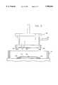
- FIG. 1is a simplified pictorial illustration of a bonding machine constructed and operative in accordance with a preferred embodiment of the present invention, with an upper chuck positioned above a lower chuck;
- FIG. 2is a simplified pictorial illustration of the bonding machine of FIG. 1 with the upper chuck applying pressure to achieve bonding of substrates;
- FIGS. 3 and 4are partial, simplified side view illustrations of the bonding machine, corresponding respectively to FIGS. 1 and 2;
- FIG. 5is a simplified top view showing a spreading pattern of an adhesive applied between the substrates being bonded, which pattern being caused by the rotation of the chucks.
- FIGS. 1-4illustrate a bonding machine 10 constructed and operative in accordance with a preferred embodiment of the present invention.
- Bonding machine 10is useful for bonding a lower substrate 12 with an upper substrate 14. (Upper substrate 14 is seen in FIGS. 3 and 4.)
- the substrates 12 and 14may be of any material suitable for bonding.
- Bonding machine 10is particularly suitable for bonding relatively delicate substrates which include sensitive components, such as in the field of microelectronics
- bonding machine 10includes a lower chuck 16 and an upper chuck 18.
- Lower chuck 16is adapted to fixedly receive the lower substrate 12
- upper chuck 18is adapted to fixedly receive the upper substrate 14, preferably each with a vacuum supplied via vacuum connectors 20 and vacuum hoses 22, such as those typically used in machine tools as is known in the art.
- Lower chuck 16includes a generally flat bed 24 and at least one engagement element 26 which preferably radially protrudes from the flat bed 24. In the illustrated embodiment there are four engagement elements 26.
- lower chuck 16is provided with a heater 28, preferably in the form of generally concentric, circular electric heating elements 30.
- a temperature sensor 32such as thermocouples or thermistors, are located in lower chuck 16, preferably embedded in flat bed 24. Temperature sensors 32 and heater 28 are connected to a temperature controller 34 for controlled heating of lower chuck 16 and lower substrate 12.
- a rotator 36is provided for rotating flat bed 24 of lower chuck 16.
- rotator 36is a variable speed servomotor, which allows for controlled rotation at varying, including optimum, speeds.
- Rotator 36may be cooled by a fluid, such as air, via a cooling conduit 38.
- Upper chuck 18includes at least one engagement arm 40 for selectable engagement with engagement elements 26.
- Each engagement arm 40preferably has a groove 42 sized such that when upper chuck 18 is lowered onto lower chuck 16, grooves 42 mate with engagement elements 26 when appropriately aligned therewith.
- engagement arms 40are aligned with engagement elements 26 by means of an orientation sensor 44 which senses the position of the engagement arms 40.
- Orientation sensor 44may be a proximity switch, such as proximity switch TL-X2C1-GE manufactured by Omron, Inc., U.S.A.
- one of the engagement arms 40is manually aligned with orientation sensor 44.
- Orientation sensor 44senses the presence of the engagement arm 40 and signals rotator 36 to rotate flat bed 24 of lower chuck 16 such that the engagement elements 26 are brought into engageable orientation with respect to the engagement arms 40.
- motion device 46for selectably moving upper chuck 18 generally vertically with respect to lower chuck 16.
- motion device 46includes a movable, pneumatic piston 48 actuated by pressurized air supplied through a conduit 50.
- Piston 48is also operative to press substrate 14 downwards upon substrate 12.
- Piston 48is preferably cooled by a fluid, such as air, via a cooling conduit 52.
- Position sensors 54may be provided along motion device 46 for accurate, controlled movement of upper chuck 18, as well as for controlling the pressure applied by upper chuck 18.
- upper chuck 18may comprise a heater and temperature sensors in addition to, or instead of, heater 28 and temperature sensors 32 of lower chuck 16.
- Adhesive 56may be any kind of adhesive, usually an epoxy.
- Adhesive 56may be any kind of adhesive, usually an epoxy.
- one partmay be applied on lower substrate 12 and the other part on upper substrate 14, as shown in FIG. 3.
- the viscosity of the adhesiveis preferably limited to a range of 400 to 2000 centipoise. A greater viscosity tends to produce non-uniform adhesion between the substrates. A lower viscosity tends to produce undesirable air bubbles between the substrates.
- one drop of a first part epoxyis applied on lower substrate 12 and one drop of the second part of the epoxy, also about 0.1 ml, is applied on upper substrate 14.
- One of the engagement arms 40is then aligned, typically manually, with orientation sensor 44 which signals rotator 36 to rotate flat bed 24 of lower chuck 16, thereby aligning engagement elements 26 with engagement arms 40.
- Piston 48is then used to carefully lower upper chuck 18 with upper substrate 14 upon lower substrate 12.
- piston 48is used to apply pressure upon the substrates 14 and 12. Typically, for microelectronics, the pressure is approximately 500 Pa.
- Heater 28in conjunction with temperature sensors 32 and controller 34, is used to heat the substrates to a desired temperature, typically approximately 65 degrees Celsius for microelectronics. As mentioned hereinabove, a heater may be additionally used to heat the substrates from upper chuck 18.
- Rotator 36is used to rotate the lower 16 and upper chucks 18.
- the chucksrotate together because the engagement elements 26 are engaged with engagement arms 40.
- the rotation speedis approximately 1500 RPM and the duration of rotation is about 2 minutes.
- FIG. 5illustrates a typical spreading pattern of the adhesive 56 as the chucks rotate.
- the rotation of the chuckscreates a centrifugal force which causes adhesive 56 to spread between the substrates 12 and 14 with a substantially uniform thickness.
- bonding machine 10produces a bond with a substantially uniform thickness of approximately 10 microns.
Landscapes
- Engineering & Computer Science (AREA)
- Mechanical Engineering (AREA)
- Physics & Mathematics (AREA)
- Thermal Sciences (AREA)
- Chemical & Material Sciences (AREA)
- Organic Chemistry (AREA)
- Fluid Mechanics (AREA)
- Adhesives Or Adhesive Processes (AREA)
Abstract
Description
Claims (7)
Applications Claiming Priority (3)
| Application Number | Priority Date | Filing Date | Title |
|---|---|---|---|
| IL113739 | 1995-05-15 | ||
| IL113739AIL113739A (en) | 1995-05-15 | 1995-05-15 | Bonding machine |
| PCT/EP1996/001747WO1996036675A1 (en) | 1995-05-15 | 1996-04-25 | Bonding machine |
Publications (1)
| Publication Number | Publication Date |
|---|---|
| US5980663Atrue US5980663A (en) | 1999-11-09 |
Family
ID=11067477
Family Applications (1)
| Application Number | Title | Priority Date | Filing Date |
|---|---|---|---|
| US08/952,019Expired - LifetimeUS5980663A (en) | 1995-05-15 | 1996-04-25 | Bonding machine |
Country Status (4)
| Country | Link |
|---|---|
| US (1) | US5980663A (en) |
| AU (1) | AU5762196A (en) |
| IL (1) | IL113739A (en) |
| WO (1) | WO1996036675A1 (en) |
Cited By (27)
| Publication number | Priority date | Publication date | Assignee | Title |
|---|---|---|---|---|
| US20010018236A1 (en)* | 1999-12-10 | 2001-08-30 | Shellcase Ltd. | Methods for producing packaged integrated circuit devices & packaged integrated circuit devices produced thereby |
| US20030216010A1 (en)* | 2002-05-20 | 2003-11-20 | Eugene Atlas | Forming a multi segment integrated circuit with isolated substrates |
| US20040021214A1 (en)* | 2002-04-16 | 2004-02-05 | Avner Badehi | Electro-optic integrated circuits with connectors and methods for the production thereof |
| US20050032391A1 (en)* | 1998-03-13 | 2005-02-10 | Semitool, Inc. | Method for processing a semiconductor wafer |
| US20050158899A1 (en)* | 2002-03-18 | 2005-07-21 | Sarcos Investments Lc | Miniaturized imaging device with integrated circuit connector system |
| US20050233498A1 (en)* | 2002-04-29 | 2005-10-20 | Texas Instruments Inc. | MEMS device wafer-level package |
| US20060022289A1 (en)* | 2002-04-16 | 2006-02-02 | Xloom Photonics, Ltd. | Electro-optical circuitry having integrated connector and methods for the production thereof |
| US7033664B2 (en) | 2002-10-22 | 2006-04-25 | Tessera Technologies Hungary Kft | Methods for producing packaged integrated circuit devices and packaged integrated circuit devices produced thereby |
| US20070285870A1 (en)* | 2006-05-26 | 2007-12-13 | Seok-Hee Shim | Adhesive chuck, and apparatus and method for assembling substrates using the same |
| US20090034085A1 (en)* | 2003-10-15 | 2009-02-05 | Xloom Communications, Ltd. | Electro-optical circuitry having integrated connector and methods for the production thereof |
| US20090065152A1 (en)* | 2007-09-12 | 2009-03-12 | Jae Seok Hwang | Adhesive chuck and substrate bonding apparatus |
| US20090093137A1 (en)* | 2007-10-08 | 2009-04-09 | Xloom Communications, (Israel) Ltd. | Optical communications module |
| US20100116428A1 (en)* | 2007-05-15 | 2010-05-13 | G.V.S. S.P.A | Method for manufacturing filtration units ad associated apparatus |
| US7787939B2 (en) | 2002-03-18 | 2010-08-31 | Sterling Lc | Miniaturized imaging device including utility aperture and SSID |
| US7835074B2 (en) | 2007-06-05 | 2010-11-16 | Sterling Lc | Mini-scope for multi-directional imaging |
| WO2011028245A1 (en) | 2009-08-26 | 2011-03-10 | Tessera, Inc. | Wafer level compliant packages for rear-face illuminated solid state image sensors |
| US7969659B2 (en) | 2008-01-11 | 2011-06-28 | Sterling Lc | Grin lens microscope system |
| WO2012061114A1 (en) | 2010-11-05 | 2012-05-10 | Digitaloptics Corporation East | Rear-face illuminated solid state image sensors |
| US8486735B2 (en) | 2008-07-30 | 2013-07-16 | Raytheon Company | Method and device for incremental wavelength variation to analyze tissue |
| US8614768B2 (en) | 2002-03-18 | 2013-12-24 | Raytheon Company | Miniaturized imaging device including GRIN lens optically coupled to SSID |
| US8690762B2 (en) | 2008-06-18 | 2014-04-08 | Raytheon Company | Transparent endoscope head defining a focal length |
| US8717428B2 (en) | 2009-10-01 | 2014-05-06 | Raytheon Company | Light diffusion apparatus |
| US8828028B2 (en) | 2009-11-03 | 2014-09-09 | Raytheon Company | Suture device and method for closing a planar opening |
| US9060704B2 (en) | 2008-11-04 | 2015-06-23 | Sarcos Lc | Method and device for wavelength shifted imaging |
| US9144664B2 (en) | 2009-10-01 | 2015-09-29 | Sarcos Lc | Method and apparatus for manipulating movement of a micro-catheter |
| US9661996B2 (en) | 2009-10-01 | 2017-05-30 | Sarcos Lc | Needle delivered imaging device |
| US9716075B2 (en) | 2010-12-21 | 2017-07-25 | Tessera, Inc. | Semiconductor chip assembly and method for making same |
Families Citing this family (7)
| Publication number | Priority date | Publication date | Assignee | Title |
|---|---|---|---|---|
| AU706524B2 (en)* | 1996-03-28 | 1999-06-17 | Matsushita Electric Industrial Co., Ltd. | Method and apparatus for laminating boards |
| KR100671071B1 (en)* | 1997-11-26 | 2007-01-17 | 코닌클리케 필립스 일렉트로닉스 엔.브이. | Apparatus and method for bonding two plate-shaped objects |
| DE19755088A1 (en)* | 1997-12-11 | 1999-06-17 | Daimler Chrysler Ag | Calibrated bonding device for bubble-free adhesive bonding of structured semiconductor wafers |
| KR100359029B1 (en)* | 2000-10-25 | 2002-10-31 | 주식회사 서울베큠테크 | Sliding type wafer bonding device with automatic spacer push and pull |
| KR20020032042A (en)* | 2000-10-25 | 2002-05-03 | 최우범 | Adjustable cone-type probe of wafer bonding chuck |
| US10698443B2 (en) | 2017-05-01 | 2020-06-30 | Microsoft Technology Licensing, Llc | Computing devices with an adhered cover and methods of manufacturing thereof |
| CN110469567B (en)* | 2018-05-12 | 2021-05-18 | 宁波方太厨具有限公司 | Water heater glass face guard subassembly bonding frock |
Citations (9)
| Publication number | Priority date | Publication date | Assignee | Title |
|---|---|---|---|---|
| DE2352707A1 (en)* | 1973-10-20 | 1975-04-24 | Max Schmidt | Plastic Christmas tree globes made from half-shells - by automatic pressing together and gluing of seam |
| GB1460461A (en)* | 1972-10-30 | 1977-01-06 | Ellemor J W | Method of manufacturing articles by joining preformed shapes |
| JPS6097820A (en)* | 1983-11-01 | 1985-05-31 | Ishida Koki Seisakusho:Kk | Manufacture of disc |
| JPS61251543A (en)* | 1985-04-26 | 1986-11-08 | Citizen Watch Co Ltd | Bonding of glass substrate |
| US4636124A (en)* | 1985-05-06 | 1987-01-13 | Illinois Tool Works Inc. | Adhesive friction weld fastener |
| NL8502514A (en)* | 1985-09-13 | 1987-04-01 | Comminvent B V | Producing playing balls, quoits etc. - comprises joining moulded half shells to form hollow cores, positioning core in mould, injecting settable material etc. |
| EP0243517A1 (en)* | 1986-04-28 | 1987-11-04 | Matsushita Electric Industrial Co., Ltd. | Method for producing information storage disk |
| US4795524A (en)* | 1986-02-07 | 1989-01-03 | Nippondenso Co., Ltd. | Apparatus for fixing cap on end of filter element |
| DE4041199A1 (en)* | 1990-12-21 | 1992-07-09 | Hamatech Halbleiter Maschinenb | Adhering twin data disk - using adhesive ring on inner side of one disc spread out by centrifugal force after second disc is placed on it |
- 1995
- 1995-05-15ILIL113739Apatent/IL113739A/ennot_activeIP Right Cessation
- 1996
- 1996-04-25WOPCT/EP1996/001747patent/WO1996036675A1/enactiveApplication Filing
- 1996-04-25AUAU57621/96Apatent/AU5762196A/ennot_activeAbandoned
- 1996-04-25USUS08/952,019patent/US5980663A/ennot_activeExpired - Lifetime
Patent Citations (9)
| Publication number | Priority date | Publication date | Assignee | Title |
|---|---|---|---|---|
| GB1460461A (en)* | 1972-10-30 | 1977-01-06 | Ellemor J W | Method of manufacturing articles by joining preformed shapes |
| DE2352707A1 (en)* | 1973-10-20 | 1975-04-24 | Max Schmidt | Plastic Christmas tree globes made from half-shells - by automatic pressing together and gluing of seam |
| JPS6097820A (en)* | 1983-11-01 | 1985-05-31 | Ishida Koki Seisakusho:Kk | Manufacture of disc |
| JPS61251543A (en)* | 1985-04-26 | 1986-11-08 | Citizen Watch Co Ltd | Bonding of glass substrate |
| US4636124A (en)* | 1985-05-06 | 1987-01-13 | Illinois Tool Works Inc. | Adhesive friction weld fastener |
| NL8502514A (en)* | 1985-09-13 | 1987-04-01 | Comminvent B V | Producing playing balls, quoits etc. - comprises joining moulded half shells to form hollow cores, positioning core in mould, injecting settable material etc. |
| US4795524A (en)* | 1986-02-07 | 1989-01-03 | Nippondenso Co., Ltd. | Apparatus for fixing cap on end of filter element |
| EP0243517A1 (en)* | 1986-04-28 | 1987-11-04 | Matsushita Electric Industrial Co., Ltd. | Method for producing information storage disk |
| DE4041199A1 (en)* | 1990-12-21 | 1992-07-09 | Hamatech Halbleiter Maschinenb | Adhering twin data disk - using adhesive ring on inner side of one disc spread out by centrifugal force after second disc is placed on it |
Cited By (52)
| Publication number | Priority date | Publication date | Assignee | Title |
|---|---|---|---|---|
| US20050032391A1 (en)* | 1998-03-13 | 2005-02-10 | Semitool, Inc. | Method for processing a semiconductor wafer |
| US7144745B2 (en) | 1999-12-10 | 2006-12-05 | Tessera Technologies Hungary Kft. | Methods for producing packaged integrated circuit devices and packaged integrated circuit devices produced |
| US20020027296A1 (en)* | 1999-12-10 | 2002-03-07 | Badehi Avner Pierre | Methods for producing packaged integrated circuit devices & packaged integrated circuit devices produced thereby |
| US7939918B2 (en) | 1999-12-10 | 2011-05-10 | Tessera Technologies Ireland Limited | Chip packages with covers |
| US20010018236A1 (en)* | 1999-12-10 | 2001-08-30 | Shellcase Ltd. | Methods for producing packaged integrated circuit devices & packaged integrated circuit devices produced thereby |
| US6777767B2 (en) | 1999-12-10 | 2004-08-17 | Shellcase Ltd. | Methods for producing packaged integrated circuit devices & packaged integrated circuit devices produced thereby |
| US20070040257A1 (en)* | 1999-12-10 | 2007-02-22 | Tessera Technologies Hungary Kft. | Chip packages with covers |
| US7787939B2 (en) | 2002-03-18 | 2010-08-31 | Sterling Lc | Miniaturized imaging device including utility aperture and SSID |
| US7591780B2 (en) | 2002-03-18 | 2009-09-22 | Sterling Lc | Miniaturized imaging device with integrated circuit connector system |
| US8614768B2 (en) | 2002-03-18 | 2013-12-24 | Raytheon Company | Miniaturized imaging device including GRIN lens optically coupled to SSID |
| US7629659B2 (en) | 2002-03-18 | 2009-12-08 | Sterling Lc | Miniaturized imaging device with integrated circuit connector system |
| US20050158899A1 (en)* | 2002-03-18 | 2005-07-21 | Sarcos Investments Lc | Miniaturized imaging device with integrated circuit connector system |
| US7166537B2 (en) | 2002-03-18 | 2007-01-23 | Sarcos Investments Lc | Miniaturized imaging device with integrated circuit connector system |
| US20060022289A1 (en)* | 2002-04-16 | 2006-02-02 | Xloom Photonics, Ltd. | Electro-optical circuitry having integrated connector and methods for the production thereof |
| US20040021214A1 (en)* | 2002-04-16 | 2004-02-05 | Avner Badehi | Electro-optic integrated circuits with connectors and methods for the production thereof |
| US20060145279A1 (en)* | 2002-04-16 | 2006-07-06 | Xloom Photonics, Ltd. | Electro-optic integrated circuits with connectors and methods for the production thereof |
| US20090246905A1 (en)* | 2002-04-16 | 2009-10-01 | Xloom Communications, Inc. | Electro-optic integrated circuits and methods for the production thereof |
| US20090154873A1 (en)* | 2002-04-16 | 2009-06-18 | Xloom Communications, (Israel) Ltd. | Electro-optic integrated circuits with connectors and methods for the production thereof |
| US8043877B2 (en) | 2002-04-16 | 2011-10-25 | Xloom Communications, Ltd. | Electro-optic integrated circuits and methods for the production thereof |
| US7466018B2 (en) | 2002-04-29 | 2008-12-16 | Texas Instruments Incorporated | MEMS device wafer-level package |
| US20050233498A1 (en)* | 2002-04-29 | 2005-10-20 | Texas Instruments Inc. | MEMS device wafer-level package |
| US20070228540A1 (en)* | 2002-04-29 | 2007-10-04 | Texas Instruments Incorporated | MEMS Device Wafer-Level Package |
| US7226810B2 (en) | 2002-04-29 | 2007-06-05 | Texas Instruments Incorporated | MEMS device wafer-level package |
| US20030216010A1 (en)* | 2002-05-20 | 2003-11-20 | Eugene Atlas | Forming a multi segment integrated circuit with isolated substrates |
| US7033664B2 (en) | 2002-10-22 | 2006-04-25 | Tessera Technologies Hungary Kft | Methods for producing packaged integrated circuit devices and packaged integrated circuit devices produced thereby |
| US20090034085A1 (en)* | 2003-10-15 | 2009-02-05 | Xloom Communications, Ltd. | Electro-optical circuitry having integrated connector and methods for the production thereof |
| US7538358B2 (en) | 2003-10-15 | 2009-05-26 | Xloom Communications, Ltd. | Electro-optical circuitry having integrated connector and methods for the production thereof |
| US20070285870A1 (en)* | 2006-05-26 | 2007-12-13 | Seok-Hee Shim | Adhesive chuck, and apparatus and method for assembling substrates using the same |
| US20110187063A1 (en)* | 2006-05-26 | 2011-08-04 | Advanced Display Process Engineering Co., Ltd. | Adhesive chuck, and apparatus and method for assembling substrates using the same |
| US8361267B2 (en) | 2006-05-26 | 2013-01-29 | Advanced Display Process Engineering Co., Ltd. | Adhesive chuck, and apparatus and method for assembling substrates using the same |
| US7921895B2 (en)* | 2006-05-26 | 2011-04-12 | Advanced Display Process Engineering Co., Ltd | Adhesive chuck, and apparatus and method for assembling substrates using the same |
| US8906186B2 (en)* | 2007-05-15 | 2014-12-09 | Gvs S.P.A. | Method for manufacturing filtration units and associated apparatus |
| US20100116428A1 (en)* | 2007-05-15 | 2010-05-13 | G.V.S. S.P.A | Method for manufacturing filtration units ad associated apparatus |
| US7835074B2 (en) | 2007-06-05 | 2010-11-16 | Sterling Lc | Mini-scope for multi-directional imaging |
| US8358462B2 (en) | 2007-06-05 | 2013-01-22 | Jacobsen Stephen C | Mini-scope for multi-directional imaging |
| US20090065152A1 (en)* | 2007-09-12 | 2009-03-12 | Jae Seok Hwang | Adhesive chuck and substrate bonding apparatus |
| US7980287B2 (en)* | 2007-09-12 | 2011-07-19 | Adp Engineering Co., Ltd. | Adhesive chuck and substrate bonding apparatus |
| US20090093137A1 (en)* | 2007-10-08 | 2009-04-09 | Xloom Communications, (Israel) Ltd. | Optical communications module |
| US7969659B2 (en) | 2008-01-11 | 2011-06-28 | Sterling Lc | Grin lens microscope system |
| US9521946B2 (en) | 2008-06-18 | 2016-12-20 | Sarcos Lc | Transparent endoscope head defining a focal length |
| US8690762B2 (en) | 2008-06-18 | 2014-04-08 | Raytheon Company | Transparent endoscope head defining a focal length |
| US8486735B2 (en) | 2008-07-30 | 2013-07-16 | Raytheon Company | Method and device for incremental wavelength variation to analyze tissue |
| US9259142B2 (en) | 2008-07-30 | 2016-02-16 | Sarcos Lc | Method and device for incremental wavelength variation to analyze tissue |
| US9060704B2 (en) | 2008-11-04 | 2015-06-23 | Sarcos Lc | Method and device for wavelength shifted imaging |
| US9717418B2 (en) | 2008-11-04 | 2017-08-01 | Sarcos Lc | Method and device for wavelength shifted imaging |
| WO2011028245A1 (en) | 2009-08-26 | 2011-03-10 | Tessera, Inc. | Wafer level compliant packages for rear-face illuminated solid state image sensors |
| US8717428B2 (en) | 2009-10-01 | 2014-05-06 | Raytheon Company | Light diffusion apparatus |
| US9144664B2 (en) | 2009-10-01 | 2015-09-29 | Sarcos Lc | Method and apparatus for manipulating movement of a micro-catheter |
| US9661996B2 (en) | 2009-10-01 | 2017-05-30 | Sarcos Lc | Needle delivered imaging device |
| US8828028B2 (en) | 2009-11-03 | 2014-09-09 | Raytheon Company | Suture device and method for closing a planar opening |
| WO2012061114A1 (en) | 2010-11-05 | 2012-05-10 | Digitaloptics Corporation East | Rear-face illuminated solid state image sensors |
| US9716075B2 (en) | 2010-12-21 | 2017-07-25 | Tessera, Inc. | Semiconductor chip assembly and method for making same |
Also Published As
| Publication number | Publication date |
|---|---|
| IL113739A0 (en) | 1995-08-31 |
| IL113739A (en) | 1998-03-10 |
| AU5762196A (en) | 1996-11-29 |
| WO1996036675A1 (en) | 1996-11-21 |
Similar Documents
| Publication | Publication Date | Title |
|---|---|---|
| US5980663A (en) | Bonding machine | |
| CN107464767B (en) | Tape stripping device | |
| EP1870926B1 (en) | Film adhesion device and film adhesion method | |
| KR102017896B1 (en) | Method for adhering works and work adhering apparatus | |
| JP2856216B2 (en) | Method of bonding adhesive tape to semiconductor wafer | |
| JP2002134438A (en) | Method and apparatus for sticking die bond tape to semiconductor wafer | |
| KR960006412Y1 (en) | Wafer Reverse Patching Device | |
| US5336319A (en) | Apparatus for applying an adhesive layer to a substrate surface | |
| CN106469658A (en) | Sheet-adhesion device and adhesion method | |
| JP4666546B2 (en) | Pressure device and bump bonding device, bonding device, and pressure bonding device using the same | |
| JP3475776B2 (en) | Flip chip bonding apparatus and flip chip bonding method | |
| JP4950478B2 (en) | PRESSURE METHOD, JOINING METHOD USING THIS METHOD, DEVICE PRODUCED BY THIS JOINING METHOD, PRESSURE DEVICE, AND JOINING DEVICE USING THE DEVICE | |
| JP2010064127A (en) | Pressing device and joining apparatus using the device, pressing method and joining process using the method | |
| JP4699644B2 (en) | Bonding device and bonding method | |
| JP2759590B2 (en) | Adhesive tape attaching method for attaching to semiconductor wafer | |
| JP2002222779A (en) | Tape sticking device and method therefor | |
| JPH04340746A (en) | Adhesive tape sticking device | |
| JPH03246953A (en) | face down bonding equipment | |
| CN106531677A (en) | Support apparatus and supporting method | |
| JP7590142B2 (en) | Sheet peeling device and sheet peeling method | |
| JP7235551B2 (en) | Peeling tape crimping device | |
| JP2848971B2 (en) | Bonding method of thin plate | |
| JPH079375Y2 (en) | Wafer bonding device | |
| JPH10189663A (en) | Bonding device | |
| JP2002205260A (en) | Wafer sticking method and device |
Legal Events
| Date | Code | Title | Description |
|---|---|---|---|
| AS | Assignment | Owner name:SHELLCASE LTD., ISRAEL Free format text:ASSIGNMENT OF ASSIGNORS INTEREST;ASSIGNOR:BADEHI, PIERRE;REEL/FRAME:009347/0823 Effective date:19980305 | |
| STCF | Information on status: patent grant | Free format text:PATENTED CASE | |
| FEPP | Fee payment procedure | Free format text:PAYOR NUMBER ASSIGNED (ORIGINAL EVENT CODE: ASPN); ENTITY STATUS OF PATENT OWNER: LARGE ENTITY | |
| FPAY | Fee payment | Year of fee payment:4 | |
| REMI | Maintenance fee reminder mailed | ||
| AS | Assignment | Owner name:TESSERA TECHNOLOGIES HUNGARY KFT., HUNGARY Free format text:ASSIGNMENT OF ASSIGNORS INTEREST;ASSIGNOR:SHELLCASE LTD., ALSO SOMETIMES KNOWN AS SHELLCASE, LTD.;REEL/FRAME:017507/0691 Effective date:20060330 | |
| AS | Assignment | Owner name:TESSERA TECHNOLOGIES HUNGARY KFT., HUNGARY Free format text:RE-RECORD ASSIGNMENT TO CORRECT STREET ADDRESS OF RECEIVING PARTY PREVIOUSLY RECORDED AT REEL/FRAME 017507/0691;ASSIGNOR:SHELLCASE LTD., ALSO SOMETIMES KNOWN AS SHELLCASE, LTD.;REEL/FRAME:017586/0949 Effective date:20060330 | |
| FEPP | Fee payment procedure | Free format text:PAT HOLDER NO LONGER CLAIMS SMALL ENTITY STATUS, ENTITY STATUS SET TO UNDISCOUNTED (ORIGINAL EVENT CODE: STOL); ENTITY STATUS OF PATENT OWNER: LARGE ENTITY | |
| FPAY | Fee payment | Year of fee payment:8 | |
| AS | Assignment | Owner name:TESSERA TECHNOLOGIES IRELAND LIMITED, IRELAND Free format text:ASSIGNMENT OF ASSIGNORS INTEREST;ASSIGNOR:TESSERA TECHNOLOGIES HUNGARY HOLDING LIMITED LIABILITY COMPANY;REEL/FRAME:025592/0734 Effective date:20101119 | |
| FPAY | Fee payment | Year of fee payment:12 | |
| AS | Assignment | Owner name:DIGITALOPTICS CORPORATION EUROPE LIMITED, CALIFOR Free format text:CHANGE OF NAME;ASSIGNOR:TESSERA TECHNOLOGIES IRELAND LIMITED;REEL/FRAME:026739/0875 Effective date:20110713 | |
| AS | Assignment | Owner name:DIGITALOPTICS CORPORATION EUROPE LIMITED, IRELAND Free format text:CORRECTION TO REEL 026739 FRAME 0875 TO CORRECTION THE ADDRESS OF RECEIVING PARTY;ASSIGNOR:TESSERA TECHNOLOGIES IRELAND LIMITED;REEL/FRAME:027137/0397 Effective date:20110713 | |
| AS | Assignment | Owner name:INVENSAS CORPORATION, CALIFORNIA Free format text:ASSIGNMENT OF ASSIGNORS INTEREST;ASSIGNOR:DIGITAL OPTICS CORPORATION EUROPE LIMITED;REEL/FRAME:030065/0817 Effective date:20130318 Owner name:INVENSAS CORPORATION, CALIFORNIA Free format text:ASSIGNMENT OF ASSIGNORS INTEREST;ASSIGNOR:DIGITALOPTICS CORPORATION EUROPE LIMITED;REEL/FRAME:030065/0817 Effective date:20130318 | |
| AS | Assignment | Owner name:ROYAL BANK OF CANADA, AS COLLATERAL AGENT, CANADA Free format text:SECURITY INTEREST;ASSIGNORS:INVENSAS CORPORATION;TESSERA, INC.;TESSERA ADVANCED TECHNOLOGIES, INC.;AND OTHERS;REEL/FRAME:040797/0001 Effective date:20161201 | |
| AS | Assignment | Owner name:DTS LLC, CALIFORNIA Free format text:RELEASE BY SECURED PARTY;ASSIGNOR:ROYAL BANK OF CANADA;REEL/FRAME:052920/0001 Effective date:20200601 Owner name:TESSERA ADVANCED TECHNOLOGIES, INC, CALIFORNIA Free format text:RELEASE BY SECURED PARTY;ASSIGNOR:ROYAL BANK OF CANADA;REEL/FRAME:052920/0001 Effective date:20200601 Owner name:IBIQUITY DIGITAL CORPORATION, MARYLAND Free format text:RELEASE BY SECURED PARTY;ASSIGNOR:ROYAL BANK OF CANADA;REEL/FRAME:052920/0001 Effective date:20200601 Owner name:INVENSAS CORPORATION, CALIFORNIA Free format text:RELEASE BY SECURED PARTY;ASSIGNOR:ROYAL BANK OF CANADA;REEL/FRAME:052920/0001 Effective date:20200601 Owner name:PHORUS, INC., CALIFORNIA Free format text:RELEASE BY SECURED PARTY;ASSIGNOR:ROYAL BANK OF CANADA;REEL/FRAME:052920/0001 Effective date:20200601 Owner name:DTS, INC., CALIFORNIA Free format text:RELEASE BY SECURED PARTY;ASSIGNOR:ROYAL BANK OF CANADA;REEL/FRAME:052920/0001 Effective date:20200601 Owner name:TESSERA, INC., CALIFORNIA Free format text:RELEASE BY SECURED PARTY;ASSIGNOR:ROYAL BANK OF CANADA;REEL/FRAME:052920/0001 Effective date:20200601 Owner name:INVENSAS BONDING TECHNOLOGIES, INC. (F/K/A ZIPTRONIX, INC.), CALIFORNIA Free format text:RELEASE BY SECURED PARTY;ASSIGNOR:ROYAL BANK OF CANADA;REEL/FRAME:052920/0001 Effective date:20200601 Owner name:FOTONATION CORPORATION (F/K/A DIGITALOPTICS CORPORATION AND F/K/A DIGITALOPTICS CORPORATION MEMS), CALIFORNIA Free format text:RELEASE BY SECURED PARTY;ASSIGNOR:ROYAL BANK OF CANADA;REEL/FRAME:052920/0001 Effective date:20200601 |