US5978256A - Non-volatile memory device using AFM and method for operating the device - Google Patents
Non-volatile memory device using AFM and method for operating the deviceDownload PDFInfo
- Publication number
- US5978256A US5978256AUS09/015,136US1513698AUS5978256AUS 5978256 AUS5978256 AUS 5978256AUS 1513698 AUS1513698 AUS 1513698AUS 5978256 AUS5978256 AUS 5978256A
- Authority
- US
- United States
- Prior art keywords
- data
- oxide film
- silicon oxide
- semiconductor device
- afm tip
- Prior art date
- Legal status (The legal status is an assumption and is not a legal conclusion. Google has not performed a legal analysis and makes no representation as to the accuracy of the status listed.)
- Expired - Lifetime
Links
Images

Classifications
- H—ELECTRICITY
- H10—SEMICONDUCTOR DEVICES; ELECTRIC SOLID-STATE DEVICES NOT OTHERWISE PROVIDED FOR
- H10B—ELECTRONIC MEMORY DEVICES
- H10B69/00—Erasable-and-programmable ROM [EPROM] devices not provided for in groups H10B41/00 - H10B63/00, e.g. ultraviolet erasable-and-programmable ROM [UVEPROM] devices
- G—PHYSICS
- G11—INFORMATION STORAGE
- G11B—INFORMATION STORAGE BASED ON RELATIVE MOVEMENT BETWEEN RECORD CARRIER AND TRANSDUCER
- G11B9/00—Recording or reproducing using a method not covered by one of the main groups G11B3/00 - G11B7/00; Record carriers therefor
- G11B9/08—Recording or reproducing using a method not covered by one of the main groups G11B3/00 - G11B7/00; Record carriers therefor using electrostatic charge injection; Record carriers therefor
- B—PERFORMING OPERATIONS; TRANSPORTING
- B82—NANOTECHNOLOGY
- B82Y—SPECIFIC USES OR APPLICATIONS OF NANOSTRUCTURES; MEASUREMENT OR ANALYSIS OF NANOSTRUCTURES; MANUFACTURE OR TREATMENT OF NANOSTRUCTURES
- B82Y10/00—Nanotechnology for information processing, storage or transmission, e.g. quantum computing or single electron logic
- G—PHYSICS
- G11—INFORMATION STORAGE
- G11B—INFORMATION STORAGE BASED ON RELATIVE MOVEMENT BETWEEN RECORD CARRIER AND TRANSDUCER
- G11B9/00—Recording or reproducing using a method not covered by one of the main groups G11B3/00 - G11B7/00; Record carriers therefor
- G11B9/12—Recording or reproducing using a method not covered by one of the main groups G11B3/00 - G11B7/00; Record carriers therefor using near-field interactions; Record carriers therefor
- G11B9/14—Recording or reproducing using a method not covered by one of the main groups G11B3/00 - G11B7/00; Record carriers therefor using near-field interactions; Record carriers therefor using microscopic probe means, i.e. recording or reproducing by means directly associated with the tip of a microscopic electrical probe as used in Scanning Tunneling Microscopy [STM] or Atomic Force Microscopy [AFM] for inducing physical or electrical perturbations in a recording medium; Record carriers or media specially adapted for such transducing of information
- G11B9/1463—Record carriers for recording or reproduction involving the use of microscopic probe means
- G11B9/149—Record carriers for recording or reproduction involving the use of microscopic probe means characterised by the memorising material or structure
- H—ELECTRICITY
- H10—SEMICONDUCTOR DEVICES; ELECTRIC SOLID-STATE DEVICES NOT OTHERWISE PROVIDED FOR
- H10D—INORGANIC ELECTRIC SEMICONDUCTOR DEVICES
- H10D64/00—Electrodes of devices having potential barriers
- H10D64/01—Manufacture or treatment
- H10D64/031—Manufacture or treatment of data-storage electrodes
- H10D64/035—Manufacture or treatment of data-storage electrodes comprising conductor-insulator-conductor-insulator-semiconductor structures
- Y—GENERAL TAGGING OF NEW TECHNOLOGICAL DEVELOPMENTS; GENERAL TAGGING OF CROSS-SECTIONAL TECHNOLOGIES SPANNING OVER SEVERAL SECTIONS OF THE IPC; TECHNICAL SUBJECTS COVERED BY FORMER USPC CROSS-REFERENCE ART COLLECTIONS [XRACs] AND DIGESTS
- Y10—TECHNICAL SUBJECTS COVERED BY FORMER USPC
- Y10S—TECHNICAL SUBJECTS COVERED BY FORMER USPC CROSS-REFERENCE ART COLLECTIONS [XRACs] AND DIGESTS
- Y10S977/00—Nanotechnology
- Y10S977/902—Specified use of nanostructure
- Y10S977/932—Specified use of nanostructure for electronic or optoelectronic application
- Y10S977/943—Information storage or retrieval using nanostructure
- Y10S977/947—Information storage or retrieval using nanostructure with scanning probe instrument
Definitions
- the present inventionrelates to a non-volatile memory device having an SiO 2 /Si laminated structure, in which nano crystals are formed in the SiO 2 layer using an atomic force microscope (AFM) and an ion implantation process, thereby being capable of operating in the same manner as EEPROM's while having a reduced size.
- the present inventionalso relates to a non-volatile memory device including an AFM tip consisting of a thin film made of a ferroelectric material (for example, PZT-PbZrxTi-xO 2 , SBT-SrBi 2 Ta 2 O 9 , etc.) and a metal layer coated over the thin film, thereby being capable of operating in a manner similar to FRAM's while having a reduced size.
- AFMatomic force microscope
- each memory cell of such semiconductor memory devicesbasically includes a capacitor adapted to accumulate voltage of a certain level and a transistor adapted to form a charge or discharge path for the voltage accumulated in the capacitor in accordance with a control signal applied thereto. Due to such a basic memory cell configuration, there is a limitation in reducing the basic size of semiconductor memory devices using known techniques.
- the present inventionhas been made in view of the above-mentioned problem, and an object of the invention is to provide a non-volatile memory device having an SiO 2 /Si laminated structure, in which nano crystals are formed in the SiO 2 layer using an atomic force microscope (AFM) and an ion implantation process, thereby being capable of operating in the same manner as EEPROM's while having a reduced size.
- AFMatomic force microscope
- Another object of the inventionis to provide a non-volatile memory device including an AFM tip consisting of a thin film made of a ferroelectric material (for example, PZT-PbZrxTi-xO 2 , SBT-SrBi 2 Ta 2 O 9 , etc.) and a metal layer coated over the thin film, thereby being capable of operating in a manner similar to FRAM's while having a reduced size.
- a ferroelectric materialfor example, PZT-PbZrxTi-xO 2 , SBT-SrBi 2 Ta 2 O 9 , etc.
- the present inventionprovides a non-volatile memory device comprising: a silicon oxide film formed to a desired thickness over a silicon substrate; and a plurality of nano crystals formed in the silicon oxide film by a conductive material implanted in the silicon oxide film, the nano crystals serving to capture free electrons existing in the silicon substrate when they are subjected to an electric field having a critical intensity or more, thereby storing data.
- the present inventionprovides a data storing method using a semiconductor device including a silicon oxide film formed to a desired thickness over a silicon substrate, and a plurality of nano crystals formed in the silicon oxide film by a conductive material implanted in the silicon oxide film, the nano crystals having a desired size capable of capturing electrons, the method comprising the steps of: disposing an atomic force microscope (AFM) tip, adapted to locally applying an electric field to a micro area, at a desired height over the semiconductor device; applying voltage of a threshold level or higher level to the AFM tip under the condition in which the height of the AFM tip is maintained, thereby effecting an electric field on a desired portion of the semiconductor device disposed beneath the AFM tip; and forcing the nano crystals formed in the silicon oxide film to capture free electrons existing in the silicon substrate by virtue of the electric field.
- AFMatomic force microscope
- the present inventionprovides a data accessing method using a semiconductor device including a silicon oxide film formed to a desired thickness over a silicon substrate, and a plurality of nano crystals formed in the silicon oxide film by a conductive material implanted in the silicon oxide film, the nano crystals having a desired size capable of capturing electrons, the semiconductor device being stored with data in a manner that free electrons are captured in a portion of the nano crystals existing in a desired micro portion of the silicon oxide film on which an electric field is locally effected, the method comprising the steps of: (a) disposing an AFM tip, adapted to locally applying an electric field to a micro area, at a desired height over the semiconductor device; (b) applying voltage of a threshold level or lower level to the AFM tip under the condition in which the height of the AFM tip is maintained; (c) scanning an upper surface of the semiconductor device by the AFM tip under the condition in which the voltage applied to the AFM tip is maintained; and (d) detecting a variation in the height of
- the present inventionprovides a data erasing method using a semiconductor device including a silicon oxide film formed to a desired thickness over a silicon substrate, and a plurality of nano crystals formed in the silicon oxide film by a conductive material implanted in the silicon oxide film, the nano crystals having a desired size capable of capturing electrons, the semiconductor device being stored with data in a manner that free electrons are captured in a portion of the nano crystals existing in a desired micro portion of the silicon oxide film on which an electric field is locally effected, the method comprising the step of: applying voltage of a critical level or higher level to an AFM tip having a desired area while scanning an optional portion of the semiconductor device, thereby effecting a reverse electric field on the scanned semiconductor device portion, so that free electrons captured in nano crystals existing in the scanned semiconductor device portion return to a channel formed in the silicon substrate.
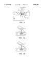
- FIG. 1is a schematic view illustrating an AFM and a sensing principle of the AFM
- FIGS. 2a to 2care schematic views respectively illustrating sequential steps of a procedure for forming a nano crystal structure in an SiO 2 /Si wafer using an ion implantation process in accordance with the present invention
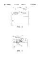
- FIG. 3is a schematic view illustrating a method for capturing electrons in proton points existing in an SiO 2 layer using an AFM tip in accordance with the present invention
- FIG. 4ais a schematic view illustrating a data reading method using an AFM in accordance with the present invention, wherein reading of data is carried out, based on a shift of an AFM tip resulting from an electric attraction force applied to the AFM tip;
- FIG. 4bis a schematic view illustrating another data reading method using an AFM in accordance with the present invention, wherein reading of data is carried out, based on a shift of an AFM tip resulting from an electric repulsion force applied to the AFM tip;
- FIG. 5is a schematic view illustrating another data reading method using an AFM in accordance with the present invention, wherein reading of data is carried out, based on a variation in capacitance depending on whether or not electrons exist;
- FIG. 6is a schematic view illustrating a data erasing method using an AFM in accordance with the present invention, wherein erasing of data is carried out in a complete manner by forcing electrons captured in all proton points existing in an SiO 2 layer to escape from the proton points;
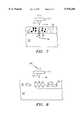
- FIG. 7is a schematic view illustrating another data erasing method using an AFM in accordance with the present invention, wherein erasing of data is carried out in a local manner by forcing electrons captured in proton points existing locally in an SiO 2 layer to escape from the proton points;
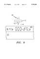
- FIG. 8is a schematic view illustrating a data storing method using an AFM in accordance with the present invention, wherein storing of data is carried out using a ferroelectric thin film in place of an SiO 2 /Si structure while generating a local minus electric field;
- FIG. 9is a schematic view illustrating another data storing method using an AFM in accordance with the present invention, wherein storing of data is carried out using a ferroelectric thin film in place of an SiO 2 /Si structure while generating a local plus electric field.
- AFM'sare configured to recognize patterns using a force existing between pure atoms, without an intermediation of electrons or atoms.
- FIG. 1an AFM is illustrated which has a very fine tip 12. When the tip 12 moves along an optional surface in such a manner that it is close to the surface, a Van der Waal's force is effected between the atoms (or molecules) existing in the tip and the atoms existing in the surface.
- the fine tip 12is disposed on a free end of a bar 11 called a "cantilever".
- the cantilever 11is vertically flexible in accordance with a physical force applied to the tip 12.
- a vertical shift of the free end of the cantilever 11 from a reference position in a state, in which no force is applied to the cantilever 11,is sensed.
- a vertical shiftis sensed using a laser 14.
- a laser beam 15 emitted from the laser 14is always focused on the free end of the cantilever 11 where the tip 12 is positioned.
- the laser beam 15is reflected from the free end of the cantilever 11 so that it is incident onto a position detector 13.
- the position detector 13Based on the incident laser beam, the position detector 13 senses the vertical shift of the cantilever.
- the position detector 13converts such a variation in the focused position of the laser beam in the form of voltage.
- the AFMis basically configured to pick up the image of an optional surface using only a Van der Waal's force effected between the atoms of the tip and surface
- the ion implantation processwhich is used in the present invention, is a process for implanting particular ions in a target wafer in an electrically accelerated state, thereby doping the wafer to have a desired doping depth and concentration.
- Si or Ge ionsare implanted in the SiO 2 layer of an SiO 2 /Si laminated structure using the ion implantation process, so as to form nano crystals in the SiO 2 layer. This procedure is illustrated in FIGS. 2a to 2c. This will be described in detail in conjunction with FIGS. 2a to 2c.
- Si ions 23 or Ge ions 24are first implanted in the SiO 2 layer 21 at an appropriate energy level.
- the reference numeral "22"denotes the bulk Si layer of the SiO 2 /Si laminated structure.
- the energy level of the ions being implantedshould be set to a level at which the implantation of those ions is stopped within the SiO 2 layer 21.
- a heat treatmentis carried out, thereby crystallizing ion-implanted portions of the SiO 2 layer. By virtue of this crystallization, proton points existing in the SiO 2 layer have a very small size.
- the resultant SiO 2 /Si laminated structurecan operate at a low operating energy level while having a reduced size as compared to known EEPROM's.
- the AFM tipis denoted by the reference numeral 12 whereas proton points in the nano crystal structure are denoted by the reference numerals 32 and 33.
- the AFM tip 12is coated with or made of a metal in order to allow voltage to be applied thereto.
- voltage of a desired levelis applied between the AFM tip 12 and the sample, electrons 34 migrate from the bulk Si layer 22, so that they are captured by proton points 32 in the SiO 2 layer 21.
- the white portions 32correspond to empty proton points containing no electrons whereas the black portions 33 correspond to proton points in which electrons are captured.
- FIG. 4aillustrates a method for reading data recorded in the SiO 2 layer 21 using the AFM tip 12 mounted on the free end of the cantilever 11 under the condition in which a electrostatic attraction force 41 is effected between the SiO 2 layer 21 and the AFM tip 12.
- a electrostatic attraction force 41is effected between the SiO 2 layer 21 and the AFM tip 12.
- FIG. 4billustrates a method for reading data recorded in the SiO 2 layer 21 by effecting an electric repulsion force 42 between the SiO 2 layer 21 and the AFM tip 12, thereby upwardly bending the cantilever 11.
- the AFM tip 12is upwardly shifted, different from the case of FIG. 4a.
- FIG. 5illustrates a method for reading data recorded in the SiO 2 layer, based on a variation in capacitance in the SiO 2 layer.
- the AFM tip 12moves along the surface of the SiO 2 layer 21, it passes electron-captured portions 26 and electron-free portions of the SiO 2 layer 21.
- C 1 ", "C 2 " and “C 3 "are the capacitance at the electron-captured portions 26, the capacitance at the electron-free portions and the capacitance at the substrate, respectively
- a variation in capacitanceis exhibited in the order of C 1 ⁇ C 2 ⁇ C 3 as the AFM tip 12 moves along the surface of the SiO 2 layer 21. Since such a variation in capacitance can be sensed by a capacitance sensor, it is possible to read data recorded in the electron-captured proton points and electron-free proton points.
- FIG. 6illustrates a method for erasing data recorded in the SiO 2 layer by returning electrons captured in the SiO 2 layer to the Si layer 22.
- a wide tip 61is used.
- an electric repulsion forceis generated.
- the wide tip 61moves along the surface of the SiO 2 layer, electrons 34 captured in proton points existing in the SiO 2 layer escape from the proton points and enter a channel formed in the Si layer.
- a wider tipit is possible to return, to the channel, electrons captured in proton points existing in a wider portion of the SiO 2 layer.
- FIG. 7illustrates a method for erasing data recorded in the SiO 2 layer in accordance with the same principle as the method of FIG. 6, except that a narrow tip 71 is used so that it effects proton points existing in a narrow portion of the SiO 2 layer.
- the tipshould have a potential lower than that in the surface of the sample, as in the case of FIG. 6. That is, a minus voltage is applied to the tip.
- the erasing of electrons captured in proton pointsis carried out in the same manner as in the case of FIG. 6. In this case, however, it is possible to erase electrons captured in a reduced number of proton points because the tip used has a reduced width.
- FIG. 8illustrates the case in which a ferroelectric thin film 81 formed over an Si wafer is used as a data storage medium in place of the above-mentioned SiO 2 /Si structure.
- a ferroelectric thin filmhas an optionally-polarized dipole structure as compared to dielectric films.
- Such a dipole structureis denoted by the reference numeral 82 in FIG. 8.
- dipolesoptionally polarized change their polarization direction in accordance with the direction of the applied electric field. The changed polarization direction of the dipoles is maintained even after the electric field or voltage is removed. This state is a state in which particular data is stored.
- FIG. 8shows the condition in which dipoles existing in the ferroelectric thin film 81 are polarized when a minus electric field 84 is applied to the AFM tip 12 of the cantilever 11. Erasing of data stored as mentioned above can be carried out in the same manner as in the case of FIG. 6 or 7. Also, reading of the data can be carried out in the above-mentioned manner.
- FIG. 9illustrates a data recording method in which a plus electric field 92 is applied to the AFM tip 12 of the cantilever 11. This method is the same as that of FIG. 8, except that the polarization direction of dipoles is opposite to that in the case of FIG. 8. It can be understood that, in this case, data different from that recorded in the case of FIG. 8 may be recorded in the same manner as in the case of FIG. 8.
- the present inventionprovides a method for fabricating a non-volatile memory device using an AFM and a method for operating such a non-volatile memory device, which are capable of achieving a storage of an increased amount of data in a reduced memory area.
Landscapes
- Engineering & Computer Science (AREA)
- Chemical & Material Sciences (AREA)
- Nanotechnology (AREA)
- Physics & Mathematics (AREA)
- Mathematical Physics (AREA)
- Theoretical Computer Science (AREA)
- Crystallography & Structural Chemistry (AREA)
- Non-Volatile Memory (AREA)
Abstract
Description
Claims (13)
Applications Claiming Priority (2)
| Application Number | Priority Date | Filing Date | Title |
|---|---|---|---|
| KR97-30776 | 1997-07-03 | ||
| KR1019970030776AKR100265692B1 (en) | 1997-07-03 | 1997-07-03 | Non-volatile memory and non-volatile memory operation method using afm |
Publications (1)
| Publication Number | Publication Date |
|---|---|
| US5978256Atrue US5978256A (en) | 1999-11-02 |
Family
ID=19513259
Family Applications (1)
| Application Number | Title | Priority Date | Filing Date |
|---|---|---|---|
| US09/015,136Expired - LifetimeUS5978256A (en) | 1997-07-03 | 1998-01-29 | Non-volatile memory device using AFM and method for operating the device |
Country Status (2)
| Country | Link |
|---|---|
| US (1) | US5978256A (en) |
| KR (1) | KR100265692B1 (en) |
Cited By (13)
| Publication number | Priority date | Publication date | Assignee | Title |
|---|---|---|---|---|
| US6562633B2 (en) | 2001-02-26 | 2003-05-13 | International Business Machines Corporation | Assembling arrays of small particles using an atomic force microscope to define ferroelectric domains |
| WO2004032149A1 (en)* | 2002-10-03 | 2004-04-15 | Koninklijke Philips Electronics N.V. | Read-only magnetic memory device mrom |
| KR100493155B1 (en)* | 2002-05-23 | 2005-06-03 | 삼성전자주식회사 | Thermally stable ferroelectric information storage apparatus |
| EP1548726A1 (en)* | 2003-12-26 | 2005-06-29 | Electronics and Telecommunications Research Institute | Data Storing and Reading Apparatus |
| US20050276143A1 (en)* | 2004-05-27 | 2005-12-15 | Cabot Microelectronics Corporation | Mobile ion memory |
| US20070272995A1 (en)* | 2006-05-23 | 2007-11-29 | Ya-Chin King | Photosensitive device |
| WO2009097643A1 (en)* | 2008-02-05 | 2009-08-13 | Qucor Pty Ltd | Fabrication of atomic scale devices |
| US20090236655A1 (en)* | 2005-12-01 | 2009-09-24 | Sam-Jong Choi | Integrated circuit device gate structures |
| US20100039138A1 (en)* | 2008-08-14 | 2010-02-18 | Nantero, Inc. | Nonvolatile nanotube programmable logic devices and a nonvolatile nanotube field programmable gate array using same |
| CZ301824B6 (en)* | 2007-08-23 | 2010-06-30 | Fyzikální ústav AV CR, v.v.i. | Process for preparing isolated groups of microscopic silicon crystals |
| CN102211754A (en)* | 2010-04-02 | 2011-10-12 | 中国科学院沈阳自动化研究所 | AFM (Atomic Force Microscopy)-based processing method of nanometer channel |
| US20160064570A1 (en)* | 2009-10-16 | 2016-03-03 | Semiconductor Energy Laboratory Co., Ltd. | Logic circuit and semiconductor device |
| US20160067387A1 (en)* | 2014-09-08 | 2016-03-10 | Venu Varanasi | Amorphous Silicon Oxide, Amorphous Silicon Oxynitride, and Amorphous Silicon Nitride Thin Films and Uses Thereof |
Families Citing this family (4)
| Publication number | Priority date | Publication date | Assignee | Title |
|---|---|---|---|---|
| JP4859292B2 (en)* | 2001-07-02 | 2012-01-25 | 富士通セミコンダクター株式会社 | Semiconductor integrated circuit device and NAND nonvolatile semiconductor device |
| KR100790861B1 (en)* | 2005-10-21 | 2008-01-03 | 삼성전자주식회사 | Resistive memory device comprising nanodot and manufacturing method for the same |
| US10060851B2 (en) | 2013-03-05 | 2018-08-28 | Plexense, Inc. | Surface plasmon detection apparatuses and methods |
| US10359362B2 (en) | 2013-04-15 | 2019-07-23 | Plexense, Inc. | Method for manufacturing nanoparticle array, surface plasmon resonance-based sensor and method for analyzing using same |
Citations (10)
| Publication number | Priority date | Publication date | Assignee | Title |
|---|---|---|---|---|
| US31083A (en)* | 1861-01-08 | James ingbam | ||
| US4217601A (en)* | 1979-02-15 | 1980-08-12 | International Business Machines Corporation | Non-volatile memory devices fabricated from graded or stepped energy band gap insulator MIM or MIS structure |
| USRE31083E (en) | 1979-02-15 | 1982-11-16 | International Business Machines Corporation | Non-volatile memory devices fabricated from graded or stepped energy band gap insulator MIM or MIS structure |
| US4939559A (en)* | 1981-12-14 | 1990-07-03 | International Business Machines Corporation | Dual electron injector structures using a conductive oxide between injectors |
| US4945515A (en)* | 1987-09-10 | 1990-07-31 | Seiko Instruments, Inc. | Memory writing apparatus |
| US4962480A (en)* | 1987-09-10 | 1990-10-09 | Seiko Instruments, Inc. | Memory reading apparatus |
| US5132934A (en)* | 1989-06-23 | 1992-07-21 | The Board Of Trustees Of The Leland Stanford Junior University | Method and apparatus for storing digital information in the form of stored charges |
| US5289402A (en)* | 1989-12-29 | 1994-02-22 | Canon Kabushiki Kaisha | Recording medium, recording method, and readout method |
| US5481527A (en)* | 1992-03-31 | 1996-01-02 | Canon Kabushiki Kaisha | Information processing apparatus with ferroelectric rewritable recording medium |
| US5608250A (en)* | 1993-11-29 | 1997-03-04 | Sgs-Thomson Microelectronics S.A. | Volatile memory cell with interface charge traps |
- 1997
- 1997-07-03KRKR1019970030776Apatent/KR100265692B1/ennot_activeExpired - Fee Related
- 1998
- 1998-01-29USUS09/015,136patent/US5978256A/ennot_activeExpired - Lifetime
Patent Citations (10)
| Publication number | Priority date | Publication date | Assignee | Title |
|---|---|---|---|---|
| US31083A (en)* | 1861-01-08 | James ingbam | ||
| US4217601A (en)* | 1979-02-15 | 1980-08-12 | International Business Machines Corporation | Non-volatile memory devices fabricated from graded or stepped energy band gap insulator MIM or MIS structure |
| USRE31083E (en) | 1979-02-15 | 1982-11-16 | International Business Machines Corporation | Non-volatile memory devices fabricated from graded or stepped energy band gap insulator MIM or MIS structure |
| US4939559A (en)* | 1981-12-14 | 1990-07-03 | International Business Machines Corporation | Dual electron injector structures using a conductive oxide between injectors |
| US4945515A (en)* | 1987-09-10 | 1990-07-31 | Seiko Instruments, Inc. | Memory writing apparatus |
| US4962480A (en)* | 1987-09-10 | 1990-10-09 | Seiko Instruments, Inc. | Memory reading apparatus |
| US5132934A (en)* | 1989-06-23 | 1992-07-21 | The Board Of Trustees Of The Leland Stanford Junior University | Method and apparatus for storing digital information in the form of stored charges |
| US5289402A (en)* | 1989-12-29 | 1994-02-22 | Canon Kabushiki Kaisha | Recording medium, recording method, and readout method |
| US5481527A (en)* | 1992-03-31 | 1996-01-02 | Canon Kabushiki Kaisha | Information processing apparatus with ferroelectric rewritable recording medium |
| US5608250A (en)* | 1993-11-29 | 1997-03-04 | Sgs-Thomson Microelectronics S.A. | Volatile memory cell with interface charge traps |
Non-Patent Citations (6)
| Title |
|---|
| Barrett et al., "Charge Storage in a Nitride-Oxide-Silicon Medium by Scanning Capaitance Microscopy", J. Appl. Phys. 70(5), Sep. 1, 1991, pp. 2725-2733. |
| Barrett et al., Charge Storage in a Nitride Oxide Silicon Medium by Scanning Capaitance Microscopy , J. Appl. Phys. 70(5), Sep. 1, 1991, pp. 2725 2733.* |
| Binnig et al "Atomic Force Microscope", Physical Review Letters vol. 56, No. 9, Mar. 3, 1986, pp. 930-933. |
| Binnig et al Atomic Force Microscope , Physical Review Letters vol. 56, No. 9, Mar. 3, 1986, pp. 930 933.* |
| Hudlet et al., "Electronic Forces Between Metallic Tip and Semiconductor Surfaces", J. Appl. Phys. 77(7), Apr. 1, 1985, pp. 3308-3314. |
| Hudlet et al., Electronic Forces Between Metallic Tip and Semiconductor Surfaces , J. Appl. Phys. 77(7), Apr. 1, 1985, pp. 3308 3314.* |
Cited By (42)
| Publication number | Priority date | Publication date | Assignee | Title |
|---|---|---|---|---|
| US6562633B2 (en) | 2001-02-26 | 2003-05-13 | International Business Machines Corporation | Assembling arrays of small particles using an atomic force microscope to define ferroelectric domains |
| KR100493155B1 (en)* | 2002-05-23 | 2005-06-03 | 삼성전자주식회사 | Thermally stable ferroelectric information storage apparatus |
| WO2004032149A1 (en)* | 2002-10-03 | 2004-04-15 | Koninklijke Philips Electronics N.V. | Read-only magnetic memory device mrom |
| EP1548726A1 (en)* | 2003-12-26 | 2005-06-29 | Electronics and Telecommunications Research Institute | Data Storing and Reading Apparatus |
| US20050141397A1 (en)* | 2003-12-26 | 2005-06-30 | Park Jong H. | Data storing and reading apparatus |
| US7656776B2 (en)* | 2003-12-26 | 2010-02-02 | Electronics And Telecommunications Research Institute | Data storing and reading apparatus for storing data in a nano-device |
| US20050276143A1 (en)* | 2004-05-27 | 2005-12-15 | Cabot Microelectronics Corporation | Mobile ion memory |
| US7277314B2 (en)* | 2004-05-27 | 2007-10-02 | Cabot Microelectronics Corporation | Mobile ion memory |
| US7964907B2 (en)* | 2005-12-01 | 2011-06-21 | Samsung Electronics Co., Ltd. | Integrated circuit device gate structures |
| US20090236655A1 (en)* | 2005-12-01 | 2009-09-24 | Sam-Jong Choi | Integrated circuit device gate structures |
| US20070272995A1 (en)* | 2006-05-23 | 2007-11-29 | Ya-Chin King | Photosensitive device |
| CZ301824B6 (en)* | 2007-08-23 | 2010-06-30 | Fyzikální ústav AV CR, v.v.i. | Process for preparing isolated groups of microscopic silicon crystals |
| CN101959790A (en)* | 2008-02-05 | 2011-01-26 | 库克有限公司 | Fabrication of Atomic Scale Devices |
| WO2009097643A1 (en)* | 2008-02-05 | 2009-08-13 | Qucor Pty Ltd | Fabrication of atomic scale devices |
| CN101959790B (en)* | 2008-02-05 | 2015-09-30 | 库克有限公司 | The manufacture of atomic-scale device |
| US8541843B2 (en) | 2008-08-14 | 2013-09-24 | Nantero Inc. | Nonvolatile nanotube programmable logic devices and a nonvolatile nanotube field programmable gate array using same |
| US20100134141A1 (en)* | 2008-08-14 | 2010-06-03 | Nantero, Inc. | Nonvolatile nanotube programmable logic devices and a nonvolatile nanotube field programmable gate array using same |
| WO2010019441A1 (en)* | 2008-08-14 | 2010-02-18 | Nantero, Inc. | Nonvolatile nanotube programmable logic devices and field programmable gate array |
| US7847588B2 (en) | 2008-08-14 | 2010-12-07 | Nantero, Inc. | Nonvolatile nanotube programmable logic devices and a nonvolatile nanotube field programmable gate array using same |
| US7852114B2 (en) | 2008-08-14 | 2010-12-14 | Nantero, Inc. | Nonvolatile nanotube programmable logic devices and a nonvolatile nanotube field programmable gate array using same |
| US20100039138A1 (en)* | 2008-08-14 | 2010-02-18 | Nantero, Inc. | Nonvolatile nanotube programmable logic devices and a nonvolatile nanotube field programmable gate array using same |
| US20100078723A1 (en)* | 2008-08-14 | 2010-04-01 | Nantero, Inc. | Nonvolatile nanotube programmable logic devices and a nonvolatile nanotube field programmable gate array using same |
| US20100079165A1 (en)* | 2008-08-14 | 2010-04-01 | Bertin Claude L | Nonvolatile nanotube programmable logic devices and a nonvolatile nanotube field programmable gate array using same |
| US8188763B2 (en) | 2008-08-14 | 2012-05-29 | Nantero, Inc. | Nonvolatile nanotube programmable logic devices and a nonvolatile nanotube field programmable gate array using same |
| US8319205B2 (en) | 2008-08-14 | 2012-11-27 | Nantero Inc. | Nonvolatile nanotube programmable logic devices and a nonvolatile nanotube field programmable gate array using same |
| US8357921B2 (en) | 2008-08-14 | 2013-01-22 | Nantero Inc. | Integrated three-dimensional semiconductor system comprising nonvolatile nanotube field effect transistors |
| US20100072459A1 (en)* | 2008-08-14 | 2010-03-25 | Nantero, Inc. | Nonvolatile nanotube programmable logic devices and a nonvolatile nanotube field programmable gate array using same |
| US10593810B2 (en) | 2009-10-16 | 2020-03-17 | Semiconductor Energy Laboratory Co., Ltd. | Logic circuit and semiconductor device |
| US20160064570A1 (en)* | 2009-10-16 | 2016-03-03 | Semiconductor Energy Laboratory Co., Ltd. | Logic circuit and semiconductor device |
| US12170338B2 (en) | 2009-10-16 | 2024-12-17 | Semiconductor Energy Laboratory Co., Ltd. | Logic circuit and semiconductor device |
| US11302824B2 (en) | 2009-10-16 | 2022-04-12 | Semiconductor Energy Laboratory Co., Ltd. | Logic circuit and semiconductor device |
| US10211344B2 (en) | 2009-10-16 | 2019-02-19 | Semiconductor Energy Laboratory Co., Ltd. | Logic circuit and semiconductor device |
| CN110061144A (en)* | 2009-10-16 | 2019-07-26 | 株式会社半导体能源研究所 | Logic circuit and semiconductor devices |
| US10490671B2 (en)* | 2009-10-16 | 2019-11-26 | Semiconductor Energy Laboratory Co., Ltd. | Logic circuit and semiconductor device |
| US11742432B2 (en) | 2009-10-16 | 2023-08-29 | Semiconductor Energy Laboratory Co., Ltd. | Logic circuit and semiconductor device |
| US10770597B2 (en) | 2009-10-16 | 2020-09-08 | Semiconductor Energy Laboratory Co., Ltd. | Logic circuit and semiconductor device |
| CN102211754A (en)* | 2010-04-02 | 2011-10-12 | 中国科学院沈阳自动化研究所 | AFM (Atomic Force Microscopy)-based processing method of nanometer channel |
| CN102211754B (en)* | 2010-04-02 | 2013-09-18 | 中国科学院沈阳自动化研究所 | AFM (Atomic Force Microscopy)-based processing method of nanometer channel |
| US10898618B2 (en)* | 2014-09-08 | 2021-01-26 | The Texas A&M University System | Amorphous silicon oxide, amorphous silicon oxynitride, and amorphous silicon nitride thin films and uses thereof |
| US20210138120A1 (en)* | 2014-09-08 | 2021-05-13 | The Texas A&M University System | Amorphous Silicon Oxide, Amorphous Silicon Oxynitride, and Amorphous Silicon Nitride Thin Films and Uses Thereof |
| US20160067387A1 (en)* | 2014-09-08 | 2016-03-10 | Venu Varanasi | Amorphous Silicon Oxide, Amorphous Silicon Oxynitride, and Amorphous Silicon Nitride Thin Films and Uses Thereof |
| US12239765B2 (en)* | 2014-09-08 | 2025-03-04 | The Texas A&M University System | Amorphous silicon oxide, amorphous silicon oxynitride, and amorphous silicon nitride thin films and uses thereof |
Also Published As
| Publication number | Publication date |
|---|---|
| KR19990008697A (en) | 1999-02-05 |
| KR100265692B1 (en) | 2000-09-15 |
Similar Documents
| Publication | Publication Date | Title |
|---|---|---|
| US5978256A (en) | Non-volatile memory device using AFM and method for operating the device | |
| US7442571B2 (en) | Semiconductor probe with resistive tip and method of fabricating the same, and information recording apparatus, information reproducing apparatus, and information measuring apparatus having the semiconductor probe | |
| US6677629B1 (en) | Electric or electronic component and application as non volatile memory and device with surface acoustic waves | |
| US5365094A (en) | Semiconductor device including ferroelectric nonvolatile memory | |
| JP2628790B2 (en) | Method and apparatus for storing digital information in the form of stored charges | |
| US6069381A (en) | Ferroelectric memory transistor with resistively coupled floating gate | |
| US6521921B2 (en) | Scanning probe microscope (SPM) probe having field effect transistor channel and method of fabricating the same | |
| US10163932B1 (en) | Memory device based on heterostructures of ferroelectric and two-dimensional materials | |
| US7813254B2 (en) | Piezoelectric reading of ferroelectric data storage media | |
| KR19980024074A (en) | Nonvolatile Memory Based on Metal-Ferroelectric-Metal-Insulator Semiconductor Structures | |
| US11100971B2 (en) | Ferroelectric domain regulated optical readout mode memory and preparing method thereof | |
| US5373462A (en) | Non-volatile storage cell of the metal - ferroelectric - semiconductor type | |
| US7994499B2 (en) | Semiconductor probe having wedge shape resistive tip and method of fabricating the same | |
| US7419843B2 (en) | Method of manufacturing semiconductor probe having resistive tip | |
| EP1120836A1 (en) | Memory cell structure integrated on semiconductor | |
| KR100734832B1 (en) | Apparatus of data storage using current switching in metal oxide layer | |
| US7671616B2 (en) | Semiconductor probe having embossed resistive tip and method of fabricating the same | |
| KR20050071956A (en) | Semiconductor memory device and manufacturing method thereof | |
| Paul et al. | Storing electronic information on semi-metal nanoparticles | |
| JPH09307073A (en) | Memory device | |
| US8068405B2 (en) | Ferroelectric memory and method in which polarity of domain of ferroelectric memory is determined using ratio of currents | |
| US7656776B2 (en) | Data storing and reading apparatus for storing data in a nano-device | |
| JPH07153858A (en) | Semiconductor memory device and manufacturing method thereof | |
| KR100190068B1 (en) | Circuit of non-volatile memory cell using ferroelectric gate capacitor | |
| US7602202B2 (en) | Semiconductor probe with high resolution resistive tip having doping control layer and method of fabricating the same |
Legal Events
| Date | Code | Title | Description |
|---|---|---|---|
| AS | Assignment | Owner name:KOREA ADVANCED INSTITUTE OF SCIENCE & TECHNOLOGY, Free format text:ASSIGNMENT OF ASSIGNORS INTEREST;ASSIGNORS:SOHN, HEE SOO;HONG, SUNG CHUL;REEL/FRAME:008979/0434 Effective date:19971202 | |
| STCF | Information on status: patent grant | Free format text:PATENTED CASE | |
| FEPP | Fee payment procedure | Free format text:PAYOR NUMBER ASSIGNED (ORIGINAL EVENT CODE: ASPN); ENTITY STATUS OF PATENT OWNER: SMALL ENTITY | |
| FPAY | Fee payment | Year of fee payment:4 | |
| FPAY | Fee payment | Year of fee payment:8 | |
| FEPP | Fee payment procedure | Free format text:PAYER NUMBER DE-ASSIGNED (ORIGINAL EVENT CODE: RMPN); ENTITY STATUS OF PATENT OWNER: SMALL ENTITY | |
| FEPP | Fee payment procedure | Free format text:PAYOR NUMBER ASSIGNED (ORIGINAL EVENT CODE: ASPN); ENTITY STATUS OF PATENT OWNER: SMALL ENTITY | |
| FEPP | Fee payment procedure | Free format text:PAYER NUMBER DE-ASSIGNED (ORIGINAL EVENT CODE: RMPN); ENTITY STATUS OF PATENT OWNER: SMALL ENTITY Free format text:PAYOR NUMBER ASSIGNED (ORIGINAL EVENT CODE: ASPN); ENTITY STATUS OF PATENT OWNER: SMALL ENTITY | |
| FPAY | Fee payment | Year of fee payment:12 | |
| AS | Assignment | Owner name:INTELLECTUAL VENTURES FUND 75 LLC, NEVADA Free format text:ASSIGNMENT OF ASSIGNORS INTEREST;ASSIGNOR:KOREA ADVANCED INSTITUTE OF SCIENCE AND TECHNOLOGY;REEL/FRAME:027142/0745 Effective date:20110627 | |
| AS | Assignment | Owner name:INTELLECTUAL VENTURES HOLDING 81 LLC, NEVADA Free format text:MERGER;ASSIGNOR:INTELLECTUAL VENTURES FUND 75 LLC;REEL/FRAME:037625/0611 Effective date:20150827 | |
| AS | Assignment | Owner name:HANGER SOLUTIONS, LLC, GEORGIA Free format text:ASSIGNMENT OF ASSIGNORS INTEREST;ASSIGNOR:INTELLECTUAL VENTURES ASSETS 158 LLC;REEL/FRAME:051486/0425 Effective date:20191206 | |
| AS | Assignment | Owner name:INTELLECTUAL VENTURES ASSETS 158 LLC, DELAWARE Free format text:ASSIGNMENT OF ASSIGNORS INTEREST;ASSIGNOR:INTELLECTUAL VENTURES HOLDING 81 LLC;REEL/FRAME:051777/0017 Effective date:20191126 | |
| AS | Assignment | Owner name:FOOTHILLS IP LLC, COLORADO Free format text:ASSIGNMENT OF ASSIGNORS INTEREST;ASSIGNOR:HANGER SOLUTIONS, LLC;REEL/FRAME:056246/0533 Effective date:20200515 |