US5977626A - Thermally and electrically enhanced PBGA package - Google Patents
Thermally and electrically enhanced PBGA packageDownload PDFInfo
- Publication number
- US5977626A US5977626AUS09/133,483US13348398AUS5977626AUS 5977626 AUS5977626 AUS 5977626AUS 13348398 AUS13348398 AUS 13348398AUS 5977626 AUS5977626 AUS 5977626A
- Authority
- US
- United States
- Prior art keywords
- substrate
- package
- die
- heat spreader
- supporting members
- Prior art date
- Legal status (The legal status is an assumption and is not a legal conclusion. Google has not performed a legal analysis and makes no representation as to the accuracy of the status listed.)
- Expired - Lifetime
Links
Images


Classifications
- H—ELECTRICITY
- H01—ELECTRIC ELEMENTS
- H01L—SEMICONDUCTOR DEVICES NOT COVERED BY CLASS H10
- H01L23/00—Details of semiconductor or other solid state devices
- H01L23/552—Protection against radiation, e.g. light or electromagnetic waves
- H—ELECTRICITY
- H01—ELECTRIC ELEMENTS
- H01L—SEMICONDUCTOR DEVICES NOT COVERED BY CLASS H10
- H01L23/00—Details of semiconductor or other solid state devices
- H01L23/28—Encapsulations, e.g. encapsulating layers, coatings, e.g. for protection
- H01L23/31—Encapsulations, e.g. encapsulating layers, coatings, e.g. for protection characterised by the arrangement or shape
- H01L23/3107—Encapsulations, e.g. encapsulating layers, coatings, e.g. for protection characterised by the arrangement or shape the device being completely enclosed
- H01L23/3121—Encapsulations, e.g. encapsulating layers, coatings, e.g. for protection characterised by the arrangement or shape the device being completely enclosed a substrate forming part of the encapsulation
- H01L23/3128—Encapsulations, e.g. encapsulating layers, coatings, e.g. for protection characterised by the arrangement or shape the device being completely enclosed a substrate forming part of the encapsulation the substrate having spherical bumps for external connection
- H—ELECTRICITY
- H01—ELECTRIC ELEMENTS
- H01L—SEMICONDUCTOR DEVICES NOT COVERED BY CLASS H10
- H01L23/00—Details of semiconductor or other solid state devices
- H01L23/34—Arrangements for cooling, heating, ventilating or temperature compensation ; Temperature sensing arrangements
- H01L23/42—Fillings or auxiliary members in containers or encapsulations selected or arranged to facilitate heating or cooling
- H01L23/433—Auxiliary members in containers characterised by their shape, e.g. pistons
- H01L23/4334—Auxiliary members in encapsulations
- H—ELECTRICITY
- H01—ELECTRIC ELEMENTS
- H01L—SEMICONDUCTOR DEVICES NOT COVERED BY CLASS H10
- H01L23/00—Details of semiconductor or other solid state devices
- H01L23/48—Arrangements for conducting electric current to or from the solid state body in operation, e.g. leads, terminal arrangements ; Selection of materials therefor
- H01L23/488—Arrangements for conducting electric current to or from the solid state body in operation, e.g. leads, terminal arrangements ; Selection of materials therefor consisting of soldered or bonded constructions
- H01L23/498—Leads, i.e. metallisations or lead-frames on insulating substrates, e.g. chip carriers
- H01L23/49811—Additional leads joined to the metallisation on the insulating substrate, e.g. pins, bumps, wires, flat leads
- H01L23/49816—Spherical bumps on the substrate for external connection, e.g. ball grid arrays [BGA]
- H—ELECTRICITY
- H01—ELECTRIC ELEMENTS
- H01L—SEMICONDUCTOR DEVICES NOT COVERED BY CLASS H10
- H01L24/00—Arrangements for connecting or disconnecting semiconductor or solid-state bodies; Methods or apparatus related thereto
- H01L24/93—Batch processes
- H01L24/95—Batch processes at chip-level, i.e. with connecting carried out on a plurality of singulated devices, i.e. on diced chips
- H01L24/97—Batch processes at chip-level, i.e. with connecting carried out on a plurality of singulated devices, i.e. on diced chips the devices being connected to a common substrate, e.g. interposer, said common substrate being separable into individual assemblies after connecting
- H—ELECTRICITY
- H01—ELECTRIC ELEMENTS
- H01L—SEMICONDUCTOR DEVICES NOT COVERED BY CLASS H10
- H01L2224/00—Indexing scheme for arrangements for connecting or disconnecting semiconductor or solid-state bodies and methods related thereto as covered by H01L24/00
- H01L2224/01—Means for bonding being attached to, or being formed on, the surface to be connected, e.g. chip-to-package, die-attach, "first-level" interconnects; Manufacturing methods related thereto
- H01L2224/10—Bump connectors; Manufacturing methods related thereto
- H01L2224/15—Structure, shape, material or disposition of the bump connectors after the connecting process
- H01L2224/16—Structure, shape, material or disposition of the bump connectors after the connecting process of an individual bump connector
- H01L2224/161—Disposition
- H01L2224/16151—Disposition the bump connector connecting between a semiconductor or solid-state body and an item not being a semiconductor or solid-state body, e.g. chip-to-substrate, chip-to-passive
- H01L2224/16221—Disposition the bump connector connecting between a semiconductor or solid-state body and an item not being a semiconductor or solid-state body, e.g. chip-to-substrate, chip-to-passive the body and the item being stacked
- H01L2224/16225—Disposition the bump connector connecting between a semiconductor or solid-state body and an item not being a semiconductor or solid-state body, e.g. chip-to-substrate, chip-to-passive the body and the item being stacked the item being non-metallic, e.g. insulating substrate with or without metallisation
- H—ELECTRICITY
- H01—ELECTRIC ELEMENTS
- H01L—SEMICONDUCTOR DEVICES NOT COVERED BY CLASS H10
- H01L2224/00—Indexing scheme for arrangements for connecting or disconnecting semiconductor or solid-state bodies and methods related thereto as covered by H01L24/00
- H01L2224/01—Means for bonding being attached to, or being formed on, the surface to be connected, e.g. chip-to-package, die-attach, "first-level" interconnects; Manufacturing methods related thereto
- H01L2224/26—Layer connectors, e.g. plate connectors, solder or adhesive layers; Manufacturing methods related thereto
- H01L2224/31—Structure, shape, material or disposition of the layer connectors after the connecting process
- H01L2224/32—Structure, shape, material or disposition of the layer connectors after the connecting process of an individual layer connector
- H01L2224/321—Disposition
- H01L2224/32151—Disposition the layer connector connecting between a semiconductor or solid-state body and an item not being a semiconductor or solid-state body, e.g. chip-to-substrate, chip-to-passive
- H01L2224/32221—Disposition the layer connector connecting between a semiconductor or solid-state body and an item not being a semiconductor or solid-state body, e.g. chip-to-substrate, chip-to-passive the body and the item being stacked
- H01L2224/32225—Disposition the layer connector connecting between a semiconductor or solid-state body and an item not being a semiconductor or solid-state body, e.g. chip-to-substrate, chip-to-passive the body and the item being stacked the item being non-metallic, e.g. insulating substrate with or without metallisation
- H—ELECTRICITY
- H01—ELECTRIC ELEMENTS
- H01L—SEMICONDUCTOR DEVICES NOT COVERED BY CLASS H10
- H01L2224/00—Indexing scheme for arrangements for connecting or disconnecting semiconductor or solid-state bodies and methods related thereto as covered by H01L24/00
- H01L2224/01—Means for bonding being attached to, or being formed on, the surface to be connected, e.g. chip-to-package, die-attach, "first-level" interconnects; Manufacturing methods related thereto
- H01L2224/26—Layer connectors, e.g. plate connectors, solder or adhesive layers; Manufacturing methods related thereto
- H01L2224/31—Structure, shape, material or disposition of the layer connectors after the connecting process
- H01L2224/32—Structure, shape, material or disposition of the layer connectors after the connecting process of an individual layer connector
- H01L2224/321—Disposition
- H01L2224/32151—Disposition the layer connector connecting between a semiconductor or solid-state body and an item not being a semiconductor or solid-state body, e.g. chip-to-substrate, chip-to-passive
- H01L2224/32221—Disposition the layer connector connecting between a semiconductor or solid-state body and an item not being a semiconductor or solid-state body, e.g. chip-to-substrate, chip-to-passive the body and the item being stacked
- H01L2224/32245—Disposition the layer connector connecting between a semiconductor or solid-state body and an item not being a semiconductor or solid-state body, e.g. chip-to-substrate, chip-to-passive the body and the item being stacked the item being metallic
- H—ELECTRICITY
- H01—ELECTRIC ELEMENTS
- H01L—SEMICONDUCTOR DEVICES NOT COVERED BY CLASS H10
- H01L2224/00—Indexing scheme for arrangements for connecting or disconnecting semiconductor or solid-state bodies and methods related thereto as covered by H01L24/00
- H01L2224/01—Means for bonding being attached to, or being formed on, the surface to be connected, e.g. chip-to-package, die-attach, "first-level" interconnects; Manufacturing methods related thereto
- H01L2224/42—Wire connectors; Manufacturing methods related thereto
- H01L2224/44—Structure, shape, material or disposition of the wire connectors prior to the connecting process
- H01L2224/45—Structure, shape, material or disposition of the wire connectors prior to the connecting process of an individual wire connector
- H01L2224/45001—Core members of the connector
- H01L2224/45099—Material
- H01L2224/451—Material with a principal constituent of the material being a metal or a metalloid, e.g. boron (B), silicon (Si), germanium (Ge), arsenic (As), antimony (Sb), tellurium (Te) and polonium (Po), and alloys thereof
- H01L2224/45138—Material with a principal constituent of the material being a metal or a metalloid, e.g. boron (B), silicon (Si), germanium (Ge), arsenic (As), antimony (Sb), tellurium (Te) and polonium (Po), and alloys thereof the principal constituent melting at a temperature of greater than or equal to 950°C and less than 1550°C
- H01L2224/45144—Gold (Au) as principal constituent
- H—ELECTRICITY
- H01—ELECTRIC ELEMENTS
- H01L—SEMICONDUCTOR DEVICES NOT COVERED BY CLASS H10
- H01L2224/00—Indexing scheme for arrangements for connecting or disconnecting semiconductor or solid-state bodies and methods related thereto as covered by H01L24/00
- H01L2224/01—Means for bonding being attached to, or being formed on, the surface to be connected, e.g. chip-to-package, die-attach, "first-level" interconnects; Manufacturing methods related thereto
- H01L2224/42—Wire connectors; Manufacturing methods related thereto
- H01L2224/47—Structure, shape, material or disposition of the wire connectors after the connecting process
- H01L2224/48—Structure, shape, material or disposition of the wire connectors after the connecting process of an individual wire connector
- H01L2224/4805—Shape
- H01L2224/4809—Loop shape
- H01L2224/48091—Arched
- H—ELECTRICITY
- H01—ELECTRIC ELEMENTS
- H01L—SEMICONDUCTOR DEVICES NOT COVERED BY CLASS H10
- H01L2224/00—Indexing scheme for arrangements for connecting or disconnecting semiconductor or solid-state bodies and methods related thereto as covered by H01L24/00
- H01L2224/01—Means for bonding being attached to, or being formed on, the surface to be connected, e.g. chip-to-package, die-attach, "first-level" interconnects; Manufacturing methods related thereto
- H01L2224/42—Wire connectors; Manufacturing methods related thereto
- H01L2224/47—Structure, shape, material or disposition of the wire connectors after the connecting process
- H01L2224/48—Structure, shape, material or disposition of the wire connectors after the connecting process of an individual wire connector
- H01L2224/481—Disposition
- H01L2224/48151—Connecting between a semiconductor or solid-state body and an item not being a semiconductor or solid-state body, e.g. chip-to-substrate, chip-to-passive
- H01L2224/48221—Connecting between a semiconductor or solid-state body and an item not being a semiconductor or solid-state body, e.g. chip-to-substrate, chip-to-passive the body and the item being stacked
- H01L2224/48225—Connecting between a semiconductor or solid-state body and an item not being a semiconductor or solid-state body, e.g. chip-to-substrate, chip-to-passive the body and the item being stacked the item being non-metallic, e.g. insulating substrate with or without metallisation
- H01L2224/48227—Connecting between a semiconductor or solid-state body and an item not being a semiconductor or solid-state body, e.g. chip-to-substrate, chip-to-passive the body and the item being stacked the item being non-metallic, e.g. insulating substrate with or without metallisation connecting the wire to a bond pad of the item
- H—ELECTRICITY
- H01—ELECTRIC ELEMENTS
- H01L—SEMICONDUCTOR DEVICES NOT COVERED BY CLASS H10
- H01L2224/00—Indexing scheme for arrangements for connecting or disconnecting semiconductor or solid-state bodies and methods related thereto as covered by H01L24/00
- H01L2224/73—Means for bonding being of different types provided for in two or more of groups H01L2224/10, H01L2224/18, H01L2224/26, H01L2224/34, H01L2224/42, H01L2224/50, H01L2224/63, H01L2224/71
- H01L2224/732—Location after the connecting process
- H01L2224/73201—Location after the connecting process on the same surface
- H01L2224/73203—Bump and layer connectors
- H01L2224/73204—Bump and layer connectors the bump connector being embedded into the layer connector
- H—ELECTRICITY
- H01—ELECTRIC ELEMENTS
- H01L—SEMICONDUCTOR DEVICES NOT COVERED BY CLASS H10
- H01L2224/00—Indexing scheme for arrangements for connecting or disconnecting semiconductor or solid-state bodies and methods related thereto as covered by H01L24/00
- H01L2224/73—Means for bonding being of different types provided for in two or more of groups H01L2224/10, H01L2224/18, H01L2224/26, H01L2224/34, H01L2224/42, H01L2224/50, H01L2224/63, H01L2224/71
- H01L2224/732—Location after the connecting process
- H01L2224/73251—Location after the connecting process on different surfaces
- H01L2224/73253—Bump and layer connectors
- H—ELECTRICITY
- H01—ELECTRIC ELEMENTS
- H01L—SEMICONDUCTOR DEVICES NOT COVERED BY CLASS H10
- H01L2224/00—Indexing scheme for arrangements for connecting or disconnecting semiconductor or solid-state bodies and methods related thereto as covered by H01L24/00
- H01L2224/73—Means for bonding being of different types provided for in two or more of groups H01L2224/10, H01L2224/18, H01L2224/26, H01L2224/34, H01L2224/42, H01L2224/50, H01L2224/63, H01L2224/71
- H01L2224/732—Location after the connecting process
- H01L2224/73251—Location after the connecting process on different surfaces
- H01L2224/73265—Layer and wire connectors
- H—ELECTRICITY
- H01—ELECTRIC ELEMENTS
- H01L—SEMICONDUCTOR DEVICES NOT COVERED BY CLASS H10
- H01L2224/00—Indexing scheme for arrangements for connecting or disconnecting semiconductor or solid-state bodies and methods related thereto as covered by H01L24/00
- H01L2224/93—Batch processes
- H01L2224/95—Batch processes at chip-level, i.e. with connecting carried out on a plurality of singulated devices, i.e. on diced chips
- H01L2224/97—Batch processes at chip-level, i.e. with connecting carried out on a plurality of singulated devices, i.e. on diced chips the devices being connected to a common substrate, e.g. interposer, said common substrate being separable into individual assemblies after connecting
- H—ELECTRICITY
- H01—ELECTRIC ELEMENTS
- H01L—SEMICONDUCTOR DEVICES NOT COVERED BY CLASS H10
- H01L24/00—Arrangements for connecting or disconnecting semiconductor or solid-state bodies; Methods or apparatus related thereto
- H01L24/01—Means for bonding being attached to, or being formed on, the surface to be connected, e.g. chip-to-package, die-attach, "first-level" interconnects; Manufacturing methods related thereto
- H01L24/42—Wire connectors; Manufacturing methods related thereto
- H01L24/44—Structure, shape, material or disposition of the wire connectors prior to the connecting process
- H01L24/45—Structure, shape, material or disposition of the wire connectors prior to the connecting process of an individual wire connector
- H—ELECTRICITY
- H01—ELECTRIC ELEMENTS
- H01L—SEMICONDUCTOR DEVICES NOT COVERED BY CLASS H10
- H01L24/00—Arrangements for connecting or disconnecting semiconductor or solid-state bodies; Methods or apparatus related thereto
- H01L24/01—Means for bonding being attached to, or being formed on, the surface to be connected, e.g. chip-to-package, die-attach, "first-level" interconnects; Manufacturing methods related thereto
- H01L24/42—Wire connectors; Manufacturing methods related thereto
- H01L24/47—Structure, shape, material or disposition of the wire connectors after the connecting process
- H01L24/48—Structure, shape, material or disposition of the wire connectors after the connecting process of an individual wire connector
- H—ELECTRICITY
- H01—ELECTRIC ELEMENTS
- H01L—SEMICONDUCTOR DEVICES NOT COVERED BY CLASS H10
- H01L24/00—Arrangements for connecting or disconnecting semiconductor or solid-state bodies; Methods or apparatus related thereto
- H01L24/73—Means for bonding being of different types provided for in two or more of groups H01L24/10, H01L24/18, H01L24/26, H01L24/34, H01L24/42, H01L24/50, H01L24/63, H01L24/71
- H—ELECTRICITY
- H01—ELECTRIC ELEMENTS
- H01L—SEMICONDUCTOR DEVICES NOT COVERED BY CLASS H10
- H01L2924/00—Indexing scheme for arrangements or methods for connecting or disconnecting semiconductor or solid-state bodies as covered by H01L24/00
- H01L2924/0001—Technical content checked by a classifier
- H01L2924/00014—Technical content checked by a classifier the subject-matter covered by the group, the symbol of which is combined with the symbol of this group, being disclosed without further technical details
- H—ELECTRICITY
- H01—ELECTRIC ELEMENTS
- H01L—SEMICONDUCTOR DEVICES NOT COVERED BY CLASS H10
- H01L2924/00—Indexing scheme for arrangements or methods for connecting or disconnecting semiconductor or solid-state bodies as covered by H01L24/00
- H01L2924/01—Chemical elements
- H01L2924/01013—Aluminum [Al]
- H—ELECTRICITY
- H01—ELECTRIC ELEMENTS
- H01L—SEMICONDUCTOR DEVICES NOT COVERED BY CLASS H10
- H01L2924/00—Indexing scheme for arrangements or methods for connecting or disconnecting semiconductor or solid-state bodies as covered by H01L24/00
- H01L2924/01—Chemical elements
- H01L2924/01029—Copper [Cu]
- H—ELECTRICITY
- H01—ELECTRIC ELEMENTS
- H01L—SEMICONDUCTOR DEVICES NOT COVERED BY CLASS H10
- H01L2924/00—Indexing scheme for arrangements or methods for connecting or disconnecting semiconductor or solid-state bodies as covered by H01L24/00
- H01L2924/01—Chemical elements
- H01L2924/01033—Arsenic [As]
- H—ELECTRICITY
- H01—ELECTRIC ELEMENTS
- H01L—SEMICONDUCTOR DEVICES NOT COVERED BY CLASS H10
- H01L2924/00—Indexing scheme for arrangements or methods for connecting or disconnecting semiconductor or solid-state bodies as covered by H01L24/00
- H01L2924/01—Chemical elements
- H01L2924/01047—Silver [Ag]
- H—ELECTRICITY
- H01—ELECTRIC ELEMENTS
- H01L—SEMICONDUCTOR DEVICES NOT COVERED BY CLASS H10
- H01L2924/00—Indexing scheme for arrangements or methods for connecting or disconnecting semiconductor or solid-state bodies as covered by H01L24/00
- H01L2924/01—Chemical elements
- H01L2924/01075—Rhenium [Re]
- H—ELECTRICITY
- H01—ELECTRIC ELEMENTS
- H01L—SEMICONDUCTOR DEVICES NOT COVERED BY CLASS H10
- H01L2924/00—Indexing scheme for arrangements or methods for connecting or disconnecting semiconductor or solid-state bodies as covered by H01L24/00
- H01L2924/01—Chemical elements
- H01L2924/01079—Gold [Au]
- H—ELECTRICITY
- H01—ELECTRIC ELEMENTS
- H01L—SEMICONDUCTOR DEVICES NOT COVERED BY CLASS H10
- H01L2924/00—Indexing scheme for arrangements or methods for connecting or disconnecting semiconductor or solid-state bodies as covered by H01L24/00
- H01L2924/01—Chemical elements
- H01L2924/01082—Lead [Pb]
- H—ELECTRICITY
- H01—ELECTRIC ELEMENTS
- H01L—SEMICONDUCTOR DEVICES NOT COVERED BY CLASS H10
- H01L2924/00—Indexing scheme for arrangements or methods for connecting or disconnecting semiconductor or solid-state bodies as covered by H01L24/00
- H01L2924/10—Details of semiconductor or other solid state devices to be connected
- H01L2924/11—Device type
- H01L2924/14—Integrated circuits
- H—ELECTRICITY
- H01—ELECTRIC ELEMENTS
- H01L—SEMICONDUCTOR DEVICES NOT COVERED BY CLASS H10
- H01L2924/00—Indexing scheme for arrangements or methods for connecting or disconnecting semiconductor or solid-state bodies as covered by H01L24/00
- H01L2924/15—Details of package parts other than the semiconductor or other solid state devices to be connected
- H01L2924/151—Die mounting substrate
- H01L2924/153—Connection portion
- H01L2924/1531—Connection portion the connection portion being formed only on the surface of the substrate opposite to the die mounting surface
- H01L2924/15311—Connection portion the connection portion being formed only on the surface of the substrate opposite to the die mounting surface being a ball array, e.g. BGA
- H—ELECTRICITY
- H01—ELECTRIC ELEMENTS
- H01L—SEMICONDUCTOR DEVICES NOT COVERED BY CLASS H10
- H01L2924/00—Indexing scheme for arrangements or methods for connecting or disconnecting semiconductor or solid-state bodies as covered by H01L24/00
- H01L2924/15—Details of package parts other than the semiconductor or other solid state devices to be connected
- H01L2924/181—Encapsulation
- H—ELECTRICITY
- H01—ELECTRIC ELEMENTS
- H01L—SEMICONDUCTOR DEVICES NOT COVERED BY CLASS H10
- H01L2924/00—Indexing scheme for arrangements or methods for connecting or disconnecting semiconductor or solid-state bodies as covered by H01L24/00
- H01L2924/30—Technical effects
- H01L2924/301—Electrical effects
- H01L2924/30107—Inductance
- H—ELECTRICITY
- H01—ELECTRIC ELEMENTS
- H01L—SEMICONDUCTOR DEVICES NOT COVERED BY CLASS H10
- H01L2924/00—Indexing scheme for arrangements or methods for connecting or disconnecting semiconductor or solid-state bodies as covered by H01L24/00
- H01L2924/30—Technical effects
- H01L2924/301—Electrical effects
- H01L2924/3011—Impedance
- H—ELECTRICITY
- H01—ELECTRIC ELEMENTS
- H01L—SEMICONDUCTOR DEVICES NOT COVERED BY CLASS H10
- H01L2924/00—Indexing scheme for arrangements or methods for connecting or disconnecting semiconductor or solid-state bodies as covered by H01L24/00
- H01L2924/30—Technical effects
- H01L2924/301—Electrical effects
- H01L2924/3025—Electromagnetic shielding
Definitions
- the present inventionrelates to an electronic device such as a semiconductor package and particular to high performance package with enhanced capability of spreading heat and electrical performance.
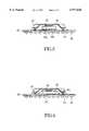
- FIG. 1shows a conventional package which includes a substrate 2, a die 4 formed on the substrate via die attach epoxy 6.
- the dieis electrically connected to the substrate 2 by using gold wire bonds 8.
- Solder balls 10 for signal transferis formed on the bottom surface of the substrate 2.
- Molding compound 12is used to cover the die 4 and gold wire bonds 8 for protection.
- the heatis spread by using thermal vias 14 formed in the substrate 2 and thermal balls 16 connected to the thermal vias 14.
- the amount heat generated by devicesis increased due to the packing density is increased. This also causes the conventional package can not meet the requirement of the future demands.
- VLSI integrated circuits packages having high connection capacityare pin grid array (PGA) and ball grid array (BGA).
- PGApin grid array
- BGAball grid array
- One such package typeis plastic ball grid array (PBGA).
- PBGAoffers many advantages over conventional packages such as solder ball I/O and high speed.
- the PBGA packagehas high speed due to a short path for signal transformation.
- the solder ballsare set on a package surface in a matrix array which can provide more signal contacts.
- pad array semiconductor devicesIn order to solve the problem relating to spread heat, pad array semiconductor devices have been proposed (see U.S. Pat. No. 5,285,352).
- the structureuses a thermal conductor in a pad array device permits routing of conductive traces and terminals beneath a semiconductor die for improved utilization of substrate area.
- An opening and a thermal conductorare set under the die on a substrate.
- the heat that is generated by devicesis dissipated to computer board via silver epoxy, the opening and a metal ground plane.
- An object of the present inventionis to provide a package with good efficiency of spreading heat and enhanced EM shielding.
- the packageincludes a substrate.
- a semiconductor chip or dieis fixedly adhered to the substrate by means of die attach material such as die attach epoxy.
- the die and the substrateare interconnected by means of signal transferring means such as bounding (gold)wires, solder ball or tape having conductive pins.
- Ball grid array (BGA), preferably, solder bumps (balls)are formed on the bottom side surface of the substrate. The solder bumps are used for external electrically coupling to the chip. At an end of each conductive trace in the substrate is connected to the solder bumps. Solder bumps are terminal of a device which permit electrical signal transfer to the chip.
- molding compoundis encapsulated among the substrate, the die and a heat spreader.
- a heat spreader or heat slugis arranged over the top surface of the substrate.
- the heat spreaderincludes a plane having a plurality of, preferably four supporting members that are set on the bottom side of the plane and at the corners of the plane.
- the supporting membersare protruded from the plane to connect the heat spreaders and the substrate.
- the heat spreaderfurther includes a protruded portion that is shaped to prevent the heat spreader from contacting with the die and the bounding wires.
- a further supporting memberis formed on the central portion of the protruded portion.
- the supporting membercan be optionally made to contact to the die or not.
- the substratehas a die paddle formed thereon for receiving the die.
- a power ringis formed around the die paddle on the surface of the substrate for power input.
- a ground ring formed around the power ring on the substratehas ground pads.
- the supporting members of the heat spreaderare connected on the ground pads by using the heat spreader attach material.
- FIG. 1is a cross sectional view of a structure of a package in accordance with the prior art.
- FIG. 2is a cross sectional view of a package in accordance with a first embodiment of the present invention.
- FIG. 3is a cross sectional view of a package in accordance with a second embodiment of the present invention.
- FIG. 4is a cross sectional view of a package in accordance with a third embodiment of the present invention.
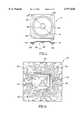
- FIG. 5is a top view and a side view of a head slug in accordance with the present invention.
- FIG. 6is a top view of the substrate in accordance with the present invention.
- FIGS. 7A-7Fshows the automatic setup process in accordance with the present invention.
- FIGS. 2-4are cross section views of the embodiments according to the present invention.
- FIG. 2illustrates a first embodiment of the present invention.
- the package 10includes a substrate 20.
- a semiconductor chip or die 22is fixedly adhered to the substrate 20 by means of die attach material such as die attach epoxy 24.
- the substratehas a first major surface and a second major surface. The first major surface is referred to a top side surface of substrate and the second major surface is referred to a bottom side surface of the substrate.
- the substrate 20includes a plurality of conductive traces (not shown), such as flexible printed circuit (PC) formed therein.
- PCflexible printed circuit
- the conductive traces of the substrate 20are used to provide electrical conductive path for signal transfer.
- the material used for the substratecan be a kind of dielectric, for example, polyimide, phenolic resin or bismaleimidetriazine (BT). Of course, any suitable material can be used for acting as the substrate.
- the conductive tracecan be selected from gold, copper or conductive metal or alloy.
- the chip (die) 22 and the substrate 20are interconnected by means of signal transferring means such as bounding wires 26.
- bounding wires 26For example, gold wires.
- the die 22is connected to the conductive traces in the substrate 20.
- the chip 22is coupled to the conductive traces.
- the conductive tracesare in the substrate for providing electrical connection path.
- One end of the bonding wireis connected to the chip 22 via a conductive pad array formed thereon, another end of the bonding wire 26 is connected to a BGA array 28 formed on the bottom side surface (second major surface) of the substrate 20 via the conductive traces 20e (FIG. 6).
- Ball grid arraypreferably, solder bumps (balls) 28, are formed on the bottom side surface of the substrate 20 by conventional positioning technique and using a solder re-flow operation.
- the solder bumps 28are used for electrically coupling to the chip 22. It is appreciate that metal alloy can be used to act the solder bumps 28.
- Solder bumps 28are terminal of a device which permit electrical signal transfer to the chip 22. In general, the solder bumps 28 are arranged in a matrix array configuration.
- the space among the substrate 20, the chip 22 and a heat spreader 32is encapsulated by molding material (compound) 30 using encapsulating technique.
- the bonding wires 20are electrically isolated by the encapsulating material 30.
- the heat spreader or heat slug 32is arranged over the top surface (first major surface) of the substrate 20 by using adhesive material 34.
- adhesive material 34For example, heat spreader attach epoxy can be used to achieve the purpose.
- the heat spreaderis exposed by the molding compound 30. This portion can improve the efficiency of spreading heat.
- the chip 22generates a lot of heat during operation.
- the heat spreader 32promotes thermal generated by the chip 22 away from the chip 22.
- the heat spreaderis formed of a kind of metal or alloy that has low thermal resistance.
- the heat spreader 32includes a plane 32a having a plurality of, preferably four supporting members 32d that are set on the bottom of the plane 32a and at the corners of the plane 32a.
- the supporting members 32dare protruded from the plane 32a.
- the supporting members 32dare used to connect the ground pad 20a to the substrate 20. More detail, the supporting members 32d and the substrate 20 are connected by means of heat spreader attaching material. In a case, epoxy or conductive glue can serve as the material to obtain the object.
- the heat spreader 32further includes a protruded portion 32b that is shaped to prevent the heat spreader 32 from contacting with the die 22 and the bonding wires 8, thereby forming a cavity 32e therein.
- the die 22is formed within the cavity 32e.
- a further supporting member 32cis formed on the central portion of the protruded portion 32b and in the cavity 32e. The supporting member 32c can be optionally made to contact to the chip 22 or not.
- FIG. 6shows the top view of the substrate 20.
- the substratehas a die paddle 20b formed thereon for receiving the die 22.
- a power ringis formed around the die paddle 20b on the surface of the substrate 20 for power input.
- a ground ring 20c formed around the power ring 20d on the substratehas ground pads 20a.
- the supporting members 32d of the heat spreader 32are connected on the ground pads 20a by using the heat spreader attach material 34.
- the present inventionfeatures the advantage of that the ground ring 20c and the heat spreader 32 construct a electric and. magnetic (EM) shielding to suppress the EM effect. This structure can reduce the inductance impedance.
- the ground pads 20aare aligned to the supporting members 32d.
- the heatis directly spread by the heat spreader 32. Additionally, the head spreader 32 is connected to the ground ring 20c of the substrate 20. Therefore, the efficiency of spreading heat is improved.
- the present inventionexhibits short signal transferring path. Further, it can improve the EM shielding effect.
- FIG. 3is a cross-sectional view of a second embodiment of the present invention. Since, in FIG. 3, like reference numerals are each assigned to the portions each corresponding to those of the first embodiment, any detailed and repeated description is omitted.
- a ball grid array (BGA), preferably, solder bumps (balls) 26aare used as the signal transferring means in lieu of the bonding wires 26 in the first embodiment.
- compound (under fill) 24ais used to take place of the die attach material 24 in FIG. 2 for filling under the die 22 and among the solder bumps 26a, substrate 20, the die 22.
- FIG. 4is a third embodiment of the present invention, only the signal transferring means is different from the first embodiment.
- a conductive tape 26bis employed to serve as the signal transferring means.
- FIG. 7A to FIG. 7Fare partial, cross-sectional views showing the assembling process in accordance with the present invention.
- the die attach epoxy 24is applied on the die paddle 20b of the substrate 20.
- the semiconductor chip or die 22is loaded on the die paddle 20b.
- a heat treatmentis used at the temperature of about 145 to 150 degrees Centigrade to fixedly adhere the die 22 to the substrate 20.
- the die 22 and the substrate 20are interconnected with the bounding wires 26 made of gold wire at the heating temperature of about 170 to 175 degrees Centigrade.
- epoxy or conductive glueis arranged on the ground pad 20a of the substrate 20 by using auto dispenser 50. Then, the heat spreader 32 is drop on the substrate and aligned the ground pad 20a to the supporting member 32d by using auto vacuum pick and place apparatus. Then, a thermal curing is performed at the temperature about 145 to 150 degrees Centigrade.
- the molding compound 30is formed over the die 22 and the heat spreader 32 for protection.
- the packageis turn up side down for implanting solder balls 28 on the surface of the substrate 20.
- the result of the assembling processis shown in FIG. 7F.
Landscapes
- Engineering & Computer Science (AREA)
- Microelectronics & Electronic Packaging (AREA)
- Physics & Mathematics (AREA)
- Computer Hardware Design (AREA)
- Power Engineering (AREA)
- Condensed Matter Physics & Semiconductors (AREA)
- General Physics & Mathematics (AREA)
- Health & Medical Sciences (AREA)
- Electromagnetism (AREA)
- Toxicology (AREA)
- Cooling Or The Like Of Semiconductors Or Solid State Devices (AREA)
Abstract
Description
Claims (28)
Priority Applications (1)
| Application Number | Priority Date | Filing Date | Title |
|---|---|---|---|
| US09/133,483US5977626A (en) | 1998-08-12 | 1998-08-12 | Thermally and electrically enhanced PBGA package |
Applications Claiming Priority (1)
| Application Number | Priority Date | Filing Date | Title |
|---|---|---|---|
| US09/133,483US5977626A (en) | 1998-08-12 | 1998-08-12 | Thermally and electrically enhanced PBGA package |
Publications (1)
| Publication Number | Publication Date |
|---|---|
| US5977626Atrue US5977626A (en) | 1999-11-02 |
Family
ID=22458826
Family Applications (1)
| Application Number | Title | Priority Date | Filing Date |
|---|---|---|---|
| US09/133,483Expired - LifetimeUS5977626A (en) | 1998-08-12 | 1998-08-12 | Thermally and electrically enhanced PBGA package |
Country Status (1)
| Country | Link |
|---|---|
| US (1) | US5977626A (en) |
Cited By (213)
| Publication number | Priority date | Publication date | Assignee | Title |
|---|---|---|---|---|
| US6163458A (en)* | 1999-12-03 | 2000-12-19 | Caesar Technology, Inc. | Heat spreader for ball grid array package |
| US6166435A (en)* | 1998-12-10 | 2000-12-26 | Industrial Technology Research Institute | Flip-chip ball grid array package with a heat slug |
| US6246115B1 (en)* | 1998-10-21 | 2001-06-12 | Siliconware Precision Industries Co., Ltd. | Semiconductor package having a heat sink with an exposed surface |
| US6249433B1 (en)* | 1999-05-14 | 2001-06-19 | Siliconware Precision Industries | Heat-dissipating device for integrated circuit package |
| US6278613B1 (en) | 2000-09-27 | 2001-08-21 | St Assembly Test Services Pte Ltd | Copper pads for heat spreader attach |
| US6284571B1 (en)* | 1997-07-02 | 2001-09-04 | Micron Technology, Inc. | Lead frame assemblies with voltage reference plane and IC packages including same |
| US6291893B1 (en)* | 1998-03-10 | 2001-09-18 | Stmicroelectronics S.R.L. | Power semiconductor device for “flip-chip” connections |
| US6380048B1 (en) | 2001-08-02 | 2002-04-30 | St Assembly Test Services Pte Ltd | Die paddle enhancement for exposed pad in semiconductor packaging |
| US6396138B1 (en)* | 2000-02-15 | 2002-05-28 | International Rectifier Corporation | Chip array with two-sided cooling |
| US6400014B1 (en) | 2001-01-13 | 2002-06-04 | Siliconware Precision Industries Co., Ltd. | Semiconductor package with a heat sink |
| US6403401B1 (en) | 2000-08-14 | 2002-06-11 | St Assembly Test Services Pte Ltd | Heat spreader hole pin 1 identifier |
| US6424032B1 (en)* | 1999-12-07 | 2002-07-23 | Fujitsu Limited | Semiconductor device having a power supply ring and a ground ring |
| US6429044B1 (en)* | 2000-08-31 | 2002-08-06 | Micron Technology, Inc. | Method and apparatus for magnetic shielding of an integrated circuit |
| US6433420B1 (en) | 2001-02-13 | 2002-08-13 | Siliconware Precision Industries Co., Ltd. | Semiconductor package with heat sink having air vent |
| US6432742B1 (en) | 2000-08-17 | 2002-08-13 | St Assembly Test Services Pte Ltd. | Methods of forming drop-in heat spreader plastic ball grid array (PBGA) packages |
| US20020119602A1 (en)* | 2001-02-23 | 2002-08-29 | Masahiro Yonemochi | Insert-moldable heat spreader, semiconductor device using same, and method for manufacturing such semiconductor device |
| US20020135065A1 (en)* | 2000-12-01 | 2002-09-26 | Zhao Sam Ziqun | Thermally and electrically enhanced ball grid array packaging |
| US20020149092A1 (en)* | 2001-04-11 | 2002-10-17 | Lee Ki Wook | Carrier frame and semiconductor package including carrier frame |
| US6472743B2 (en) | 2001-02-22 | 2002-10-29 | Siliconware Precision Industries, Co., Ltd. | Semiconductor package with heat dissipating structure |
| US20020190361A1 (en)* | 2000-12-22 | 2002-12-19 | Zhao Sam Z. | Die-up ball grid array package with die-attached heat spreader |
| US20020195704A1 (en)* | 2001-06-21 | 2002-12-26 | Vincent Chan | Multi-die module and method thereof |
| US6504723B1 (en)* | 2001-11-15 | 2003-01-07 | Intel Corporation | Electronic assembly having solder thermal interface between a die substrate and a heat spreader |
| US6507102B2 (en) | 1999-05-12 | 2003-01-14 | Amkor Technology, Inc. | Printed circuit board with integral heat sink for semiconductor package |
| US6507104B2 (en) | 2000-09-07 | 2003-01-14 | Siliconware Precision Industries Co., Ltd. | Semiconductor package with embedded heat-dissipating device |
| US20030015785A1 (en)* | 1995-11-29 | 2003-01-23 | Hitachi, Ltd. | BGA type semiconductor device and electronic equipment using the same |
| US6525421B1 (en)* | 2001-05-01 | 2003-02-25 | Lsi Logic Corporation | Molded integrated circuit package |
| US6528876B2 (en)* | 2000-06-26 | 2003-03-04 | Siliconware Precision Industries Co., Ltd. | Semiconductor package having heat sink attached to substrate |
| US6528872B2 (en)* | 2001-04-19 | 2003-03-04 | Via Technologies, Inc. | Packaging structure for ball grid array |
| WO2003021670A1 (en)* | 2001-07-31 | 2003-03-13 | Chippac, Inc. | Plastic ball grid array package with integral heatsink |
| US6534859B1 (en)* | 2002-04-05 | 2003-03-18 | St. Assembly Test Services Ltd. | Semiconductor package having heat sink attached to pre-molded cavities and method for creating the package |
| KR20030023986A (en)* | 2001-09-14 | 2003-03-26 | 주동욱 | Method of ensuring adhesivity and electric conductivity in a PBGA heat-slug |
| US20030057550A1 (en)* | 2000-12-22 | 2003-03-27 | Broadcom Corporation | Ball grid array package enhanced with a thermal and electrical connector |
| US6541854B2 (en)* | 2000-12-01 | 2003-04-01 | Siliconware Precision Industries Co., Ltd. | Super low profile package with high efficiency of heat dissipation |
| US6541310B1 (en) | 2000-07-24 | 2003-04-01 | Siliconware Precision Industries Co., Ltd. | Method of fabricating a thin and fine ball-grid array package with embedded heat spreader |
| US6549413B2 (en) | 2001-02-27 | 2003-04-15 | Chippac, Inc. | Tape ball grid array semiconductor package structure and assembly process |
| US6552428B1 (en)* | 1998-10-12 | 2003-04-22 | Siliconware Precision Industries Co., Ltd. | Semiconductor package having an exposed heat spreader |
| US20030077853A1 (en)* | 1997-07-02 | 2003-04-24 | Kinsman Larry D. | Varied-thickness heat sink for integrated circuit (IC) packages and method of fabricating IC packages |
| US20030098469A1 (en)* | 2000-09-25 | 2003-05-29 | Micron Technology, Inc. | Shielding arrangement to protect a circuit from stray magnetic fields |
| US20030111726A1 (en)* | 2001-12-18 | 2003-06-19 | Khan Reza-Ur Rahman | Ball grid array package substrates and method of making the same |
| US20030132494A1 (en)* | 2002-01-15 | 2003-07-17 | Tuttle Mark E | Magnetic shield for integrated circuit packaging |
| KR100392061B1 (en)* | 2001-09-14 | 2003-07-22 | 주동욱 | Method of ensuring against electrical risk in a drop-in type PBGA |
| US6599779B2 (en) | 2001-09-24 | 2003-07-29 | St Assembly Test Service Ltd. | PBGA substrate for anchoring heat sink |
| US20030146506A1 (en)* | 2002-02-01 | 2003-08-07 | Broadcom Corporation | Ball grid array package fabrication with IC die support structures |
| US20030146511A1 (en)* | 2002-02-01 | 2003-08-07 | Broadcom Corporation | Ball grid array package with multiple interposers |
| US20030146503A1 (en)* | 2002-02-01 | 2003-08-07 | Broadcom Corporation | Ball grid array package with stepped stiffener layer |
| US6618252B2 (en)* | 2001-06-11 | 2003-09-09 | Samsung Electro-Mechanics Co., Ltd. | Heat sink of module with built-in IC |
| US20030168720A1 (en)* | 2002-03-06 | 2003-09-11 | Nichia Corporation | Semiconductor device and manufacturing method for same |
| US20030179556A1 (en)* | 2002-03-21 | 2003-09-25 | Broadcom Corporation | Enhanced die-up ball grid array package with two substrates and method for making the same |
| SG99859A1 (en)* | 1999-05-07 | 2003-11-27 | St Assembly Test Services Ltd | Heat sink for ball grid array packages |
| US6657294B2 (en)* | 2000-05-23 | 2003-12-02 | Koninklijke Philips Electronics N.V. | Data carrier having an IC module with a protection mechanism for protecting the parts of the IC module from mechanical stress |
| US6657293B1 (en)* | 1999-10-05 | 2003-12-02 | Nec Corporation | Chip scale package in which layout of wiring lines is improved |
| US20030231032A1 (en)* | 2002-06-13 | 2003-12-18 | Takayuki Tanaka | Multistage level discrimination circuit |
| US6667546B2 (en)* | 2001-11-15 | 2003-12-23 | Siliconware Precision Industries Co., Ltd. | Ball grid array semiconductor package and substrate without power ring or ground ring |
| US20040012096A1 (en)* | 2002-07-16 | 2004-01-22 | Ji Yon Kim | Stack-type semiconductor package having one or more semiconductor packages stacked therein |
| US20040018666A1 (en)* | 2002-04-19 | 2004-01-29 | Chun-Chi Lee | Wafer level package structure and method for packaging the same |
| US6706563B2 (en) | 2002-04-10 | 2004-03-16 | St Assembly Test Services Pte Ltd | Heat spreader interconnect methodology for thermally enhanced PBGA packages |
| US6717241B1 (en)* | 2000-08-31 | 2004-04-06 | Micron Technology, Inc. | Magnetic shielding for integrated circuits |
| US6720649B2 (en)* | 2001-12-07 | 2004-04-13 | Siliconware Precision Industries Co., Ltd. | Semiconductor package with heat dissipating structure |
| EP1347513A3 (en)* | 2002-03-22 | 2004-04-14 | Broadcom Corporation | Low voltage drop and high thermal performance ball grid array package |
| US6737298B2 (en) | 2002-01-23 | 2004-05-18 | St Assembly Test Services Ltd | Heat spreader anchoring & grounding method & thermally enhanced PBGA package using the same |
| US6737755B1 (en)* | 2002-07-19 | 2004-05-18 | Asat, Ltd. | Ball grid array package with improved thermal characteristics |
| US6747350B1 (en) | 2003-06-06 | 2004-06-08 | Silicon Integrated Systems Corp. | Flip chip package structure |
| US20040124515A1 (en)* | 2002-12-31 | 2004-07-01 | Su Tao | [chip package structure and method for manufacturing the same] |
| US20040188864A1 (en)* | 2003-03-28 | 2004-09-30 | United Test & Assembly Center Ltd. | Packaged device and method of packaging |
| US20040212051A1 (en)* | 2000-12-22 | 2004-10-28 | Broadcom Corporation | Ball grid array package with patterned stiffener layer |
| WO2004032186A3 (en)* | 2002-09-30 | 2004-10-28 | Advanced Interconnect Tech Ltd | Thermal enhanced package for block mold assembly |
| KR100456816B1 (en)* | 2000-06-13 | 2004-11-10 | 앰코 테크놀로지 코리아 주식회사 | Semiconductor package |
| US20040245936A1 (en)* | 2003-06-03 | 2004-12-09 | Flower Graham Mcrae | Integrated circuit device for driving a laser diode with reduced heat transfer and method for fabricating the device |
| US20040262746A1 (en)* | 2003-06-28 | 2004-12-30 | Samsung Electro-Mechanics Co., Ltd. | High-density chip scale package and method of manufacturing the same |
| US6849940B1 (en)* | 2000-11-20 | 2005-02-01 | Ati Technologies, Inc. | Integrated circuit package for the transfer of heat generated by the inte circuit and method of fabricating same |
| WO2005010989A1 (en)* | 2003-07-30 | 2005-02-03 | Koninklijke Philips Electronics, N.V. | Ground arch for wirebond ball grid arrays |
| US6853070B2 (en) | 2001-02-15 | 2005-02-08 | Broadcom Corporation | Die-down ball grid array package with die-attached heat spreader and method for making the same |
| US20050062149A1 (en)* | 2001-06-26 | 2005-03-24 | Chippac, Inc | Integral heatsink ball grid array |
| US6882041B1 (en)* | 2002-02-05 | 2005-04-19 | Altera Corporation | Thermally enhanced metal capped BGA package |
| US20050093135A1 (en)* | 2003-10-31 | 2005-05-05 | Wei-Chi Liu | Thermal dissipating element of a chip |
| US20050104201A1 (en)* | 2003-11-18 | 2005-05-19 | Advanced Semiconductor Engineering, Inc. | Heat spreader and semiconductor device package having the same |
| US20050104165A1 (en)* | 2002-05-22 | 2005-05-19 | Sharp Kabushiki Kaisha | Semiconductor element, semiconductor device, and method for manufacturing semiconductor element |
| US20050145277A1 (en)* | 2001-12-04 | 2005-07-07 | Arch Chemicals, Inc., A Corporation Of The State Of Connecticut | Chemical feeder |
| US6919631B1 (en) | 2001-12-07 | 2005-07-19 | Amkor Technology, Inc. | Structures for improving heat dissipation in stacked semiconductor packages |
| US6933176B1 (en) | 2002-07-19 | 2005-08-23 | Asat Ltd. | Ball grid array package and process for manufacturing same |
| US20050224954A1 (en)* | 2004-04-08 | 2005-10-13 | Kelly Michael G | Thermal dissipation in integrated circuit systems |
| US6969640B1 (en) | 2004-09-02 | 2005-11-29 | Stats Chippac Ltd. | Air pocket resistant semiconductor package system |
| KR100533763B1 (en)* | 2002-10-29 | 2005-12-06 | 앰코 테크놀로지 코리아 주식회사 | semiconductor package |
| US20050275086A1 (en)* | 2004-06-09 | 2005-12-15 | Lsi Logic Corporation | Semiconductor package and process utilizing pre-formed mold cap and heatspreader assembly |
| US20050281011A1 (en)* | 2004-06-22 | 2005-12-22 | Lim Hong T | Heat spreader in integrated circuit package |
| US6979594B1 (en) | 2002-07-19 | 2005-12-27 | Asat Ltd. | Process for manufacturing ball grid array package |
| US6982192B1 (en)* | 1999-12-30 | 2006-01-03 | Intel Corporation | High performance thermal interface curing process for organic flip chip packages |
| US20060055006A1 (en)* | 2004-09-16 | 2006-03-16 | Rosemount Inc. | Field device incorporating circuit card assembly as environmental and EMI/RFI shield |
| US20060063306A1 (en)* | 2004-09-23 | 2006-03-23 | Ki-Won Choi | Semiconductor package having a heat slug and manufacturing method thereof |
| US20060094161A1 (en)* | 2002-12-30 | 2006-05-04 | Advanced Semiconductor Engineering, Inc. | Thermal enhance package and manufacturing method thereof |
| US20060103008A1 (en)* | 2004-11-15 | 2006-05-18 | Stats Chippac Ltd. | Hyper thermally enhanced semiconductor package system |
| US20060131735A1 (en)* | 2004-11-15 | 2006-06-22 | Stats Chippac Ltd. | Hyper thermally enhanced semiconductor package system |
| US20060231944A1 (en)* | 2005-04-15 | 2006-10-19 | Siliconware Precision Industries Co., Ltd. | Thermally enhanced semiconductor package and fabrication method thereof |
| US7126218B1 (en)* | 2001-08-07 | 2006-10-24 | Amkor Technology, Inc. | Embedded heat spreader ball grid array |
| US7132744B2 (en) | 2000-12-22 | 2006-11-07 | Broadcom Corporation | Enhanced die-up ball grid array packages and method for making the same |
| US20060273467A1 (en)* | 2005-06-06 | 2006-12-07 | Delphi Technologies, Inc. | Flip chip package and method of conducting heat therefrom |
| US20070045829A1 (en)* | 2005-08-30 | 2007-03-01 | Samsung Electro-Mechanics Co., Ltd. | Backside ground type flip chip semiconductor package |
| US20070065984A1 (en)* | 2005-09-22 | 2007-03-22 | Lau Daniel K | Thermal enhanced package for block mold assembly |
| US20070090533A1 (en)* | 2005-10-24 | 2007-04-26 | Texas Instruments Incorporated | Closed loop thermally enhanced flip chip BGA |
| US20070090502A1 (en)* | 2005-10-20 | 2007-04-26 | Broadcom Corporation | Methods and apparatus for improved thermal performance and electromagnetic interference (EMI) shielding in leadframe integrated circuit (IC) packages |
| US20070107525A1 (en)* | 2005-11-17 | 2007-05-17 | Schnaare Theodore H | Process transmitter with overpressure vent |
| US7259457B2 (en) | 2001-05-07 | 2007-08-21 | Broadcom Corporation | Die-up ball grid array package including a substrate capable of mounting an integrated circuit die and method for making the same |
| US20070200210A1 (en)* | 2006-02-28 | 2007-08-30 | Broadcom Corporation | Methods and apparatus for improved thermal performance and electromagnetic interference (EMI) shielding in integrated circuit (IC) packages |
| US20070200207A1 (en)* | 2006-02-28 | 2007-08-30 | Ramos Mary J B | No lead package with heat spreader |
| US20070284733A1 (en)* | 2006-06-08 | 2007-12-13 | Advanced Interconnect Technologies Limited, A Corporation Of Mauritius. | Method of making thermally enhanced substrate-base package |
| US20080017975A1 (en)* | 2006-06-30 | 2008-01-24 | Carl Deppisch | Capillary underflow integral heat spreader |
| US20080019112A1 (en)* | 2004-10-28 | 2008-01-24 | Kyocera Corporation | Electronic Component Module and Radio Communications Equipment |
| US20080067645A1 (en)* | 2006-09-20 | 2008-03-20 | Chee Seng Foong | Heat spreader for semiconductor package |
| US7372151B1 (en) | 2003-09-12 | 2008-05-13 | Asat Ltd. | Ball grid array package and process for manufacturing same |
| WO2008063744A1 (en)* | 2006-11-17 | 2008-05-29 | Freescale Semiconductor Inc. | Method of packaging a device having a keypad switch point |
| US20080122067A1 (en)* | 2006-11-27 | 2008-05-29 | Chung-Cheng Wang | Heat spreader for an electrical device |
| US20080157344A1 (en)* | 2006-12-28 | 2008-07-03 | Siliconware Precision Industries Co., Ltd. | Heat dissipation semiconductor pakage |
| US7411281B2 (en) | 2004-06-21 | 2008-08-12 | Broadcom Corporation | Integrated circuit device package having both wire bond and flip-chip interconnections and method of making the same |
| US20080211089A1 (en)* | 2007-02-16 | 2008-09-04 | Broadcom Corporation | Interposer for die stacking in semiconductor packages and the method of making the same |
| US7432586B2 (en) | 2004-06-21 | 2008-10-07 | Broadcom Corporation | Apparatus and method for thermal and electromagnetic interference (EMI) shielding enhancement in die-up array packages |
| USD580376S1 (en)* | 2006-10-12 | 2008-11-11 | Semi-Photonics Co., Ltd. | Lead frame for a four-pin light-emitting diode device |
| USD580375S1 (en)* | 2006-10-12 | 2008-11-11 | Semi-Photonics Co., Ltd. | Lead frame for a two-pin light emitting diode device |
| US20080277777A1 (en)* | 2007-05-11 | 2008-11-13 | Siliconware Precision Industries Co., Ltd. | Heat dissipation semiconductor package |
| USD582360S1 (en)* | 2006-10-12 | 2008-12-09 | Semi-Photonics Co., Ltd. | Lead frame for a through-hole light emitting diode device |
| US20080305584A1 (en)* | 2007-06-08 | 2008-12-11 | Chee Seng Foong | Heat spreader for center gate molding |
| US20080303124A1 (en)* | 2007-06-08 | 2008-12-11 | Broadcom Corporation | Lead frame-BGA package with enhanced thermal performance and I/O counts |
| US20090000114A1 (en)* | 2007-06-27 | 2009-01-01 | Rf Micro Devices, Inc. | Heat sink formed with conformal shield |
| US7482686B2 (en) | 2004-06-21 | 2009-01-27 | Braodcom Corporation | Multipiece apparatus for thermal and electromagnetic interference (EMI) shielding enhancement in die-up array packages and method of making the same |
| US20090035895A1 (en)* | 2007-07-30 | 2009-02-05 | Advanced Semiconductor Engineering, Inc. | Chip package and chip packaging process thereof |
| US20090072362A1 (en)* | 2005-12-09 | 2009-03-19 | Fairchild Semiconductor Corporation | Thermal enhanced upper and dual heat sink exposed molded leadless package |
| US20090121334A1 (en)* | 2007-11-09 | 2009-05-14 | Shinko Electric Industries Co., Ltd. | Manufacturing method of semiconductor apparatus and semiconductor apparatus |
| US20090152688A1 (en)* | 2007-12-13 | 2009-06-18 | Byung Tai Do | Integrated circuit package system for shielding electromagnetic interference |
| US7550845B2 (en) | 2002-02-01 | 2009-06-23 | Broadcom Corporation | Ball grid array package with separated stiffener layer |
| US20090166830A1 (en)* | 2007-12-28 | 2009-07-02 | Kuan-Hsing Li | Metallic cover of miniaturization module |
| US20090194868A1 (en)* | 2008-02-01 | 2009-08-06 | National Semiconductor Corporation | Panel level methods and systems for packaging integrated circuits with integrated heat sinks |
| US20090256244A1 (en)* | 2008-02-05 | 2009-10-15 | Kuo-Hsien Liao | Semiconductor device packages with electromagnetic interference shielding |
| USD613702S1 (en)* | 2006-10-12 | 2010-04-13 | SemiLEDs Optoelectronics Co., Ltd. | Two-pin lead frame for a LED device |
| US20100110656A1 (en)* | 2008-10-31 | 2010-05-06 | Advanced Semiconductor Engineering, Inc. | Chip package and manufacturing method thereof |
| US20100109152A1 (en)* | 2008-10-30 | 2010-05-06 | Nec Electronics Corporation | Electronic device and lid |
| US7714453B2 (en) | 2006-05-12 | 2010-05-11 | Broadcom Corporation | Interconnect structure and formation for package stacking of molded plastic area array package |
| US20100207259A1 (en)* | 2008-02-05 | 2010-08-19 | Advanced Semiconductor Engineering, Inc. | Semiconductor device packages with electromagnetic interference shielding |
| US20100207258A1 (en)* | 2009-02-19 | 2010-08-19 | Advanced Semiconductor Engineering, Inc. | Chip package and manufacturing method thereof |
| US7786591B2 (en) | 2004-09-29 | 2010-08-31 | Broadcom Corporation | Die down ball grid array package |
| US20100224991A1 (en)* | 2006-07-11 | 2010-09-09 | Filoteo Jr Dario S | Integrated circuit heat spreader stacking system |
| US7808087B2 (en) | 2006-06-01 | 2010-10-05 | Broadcom Corporation | Leadframe IC packages having top and bottom integrated heat spreaders |
| US20100308453A1 (en)* | 2009-06-03 | 2010-12-09 | Honeywell International Inc. | Integrated circuit package including a thermally and electrically conductive package lid |
| US20100327421A1 (en)* | 2009-06-30 | 2010-12-30 | Stmicroelectronics Asia Pacific Pte. Ltd. | Ic package design with stress relief feature |
| US20110006408A1 (en)* | 2009-07-13 | 2011-01-13 | Advanced Semiconductor Engineering, Inc. | Chip package and manufacturing method thereof |
| US20110012257A1 (en)* | 2009-07-14 | 2011-01-20 | Freescale Semiconductor, Inc | Heat spreader for semiconductor package |
| US20110044007A1 (en)* | 2009-08-20 | 2011-02-24 | Nec Electronics Corporation | Heat sink, semiconductor device, and method of manufacturing heat sink |
| US20110070700A1 (en)* | 2007-05-16 | 2011-03-24 | Texas Instruments Incorporated | Apparatus for Connecting Integrated Circuit Chip to Power and Ground Circuits |
| US7999371B1 (en) | 2010-02-09 | 2011-08-16 | Amkor Technology, Inc. | Heat spreader package and method |
| US8018072B1 (en)* | 2008-12-23 | 2011-09-13 | Amkor Technology, Inc. | Semiconductor package having a heat spreader with an exposed exterion surface and a top mold gate |
| US8022511B2 (en) | 2008-02-05 | 2011-09-20 | Advanced Semiconductor Engineering, Inc. | Semiconductor device packages with electromagnetic interference shielding |
| US8030750B2 (en) | 2009-11-19 | 2011-10-04 | Advanced Semiconductor Engineering, Inc. | Semiconductor device packages with electromagnetic interference shielding |
| US8053872B1 (en)* | 2007-06-25 | 2011-11-08 | Rf Micro Devices, Inc. | Integrated shield for a no-lead semiconductor device package |
| US20110278714A1 (en)* | 2010-05-14 | 2011-11-17 | Chipmos Technologies Inc. | Chip package device and manufacturing method thereof |
| US8062930B1 (en) | 2005-08-08 | 2011-11-22 | Rf Micro Devices, Inc. | Sub-module conformal electromagnetic interference shield |
| US20120104581A1 (en)* | 2010-11-02 | 2012-05-03 | Global Unichip Corporation | Semiconductor package device with a heat dissipation structure and the packaging method thereof |
| US20120112328A1 (en)* | 2009-03-23 | 2012-05-10 | Stats Chippac, Ltd. | Semiconductor Device and Method of Mounting Pre-Fabricated Shielding Frame over Semiconductor Die |
| US8183680B2 (en) | 2006-05-16 | 2012-05-22 | Broadcom Corporation | No-lead IC packages having integrated heat spreader for electromagnetic interference (EMI) shielding and thermal enhancement |
| US8350367B2 (en) | 2008-02-05 | 2013-01-08 | Advanced Semiconductor Engineering, Inc. | Semiconductor device packages with electromagnetic interference shielding |
| US8368185B2 (en) | 2009-11-19 | 2013-02-05 | Advanced Semiconductor Engineering, Inc. | Semiconductor device packages with electromagnetic interference shielding |
| US8378466B2 (en) | 2009-11-19 | 2013-02-19 | Advanced Semiconductor Engineering, Inc. | Wafer-level semiconductor device packages with electromagnetic interference shielding |
| US8410584B2 (en) | 2008-08-08 | 2013-04-02 | Advanced Semiconductor Engineering, Inc. | Semiconductor device packages with electromagnetic interference shielding |
| US8421212B2 (en) | 2010-09-22 | 2013-04-16 | Stats Chippac Ltd. | Integrated circuit packaging system with active surface heat removal and method of manufacture thereof |
| US20130155620A1 (en)* | 2011-12-20 | 2013-06-20 | Stmicroelectronics (Grenoble 2) Sas | Package |
| US8476115B2 (en) | 2011-05-03 | 2013-07-02 | Stats Chippac, Ltd. | Semiconductor device and method of mounting cover to semiconductor die and interposer with adhesive material |
| CN103219298A (en)* | 2012-05-15 | 2013-07-24 | 日月光半导体制造股份有限公司 | Semiconductor package with heat dissipation structure and electromagnetic interference shielding and manufacturing method thereof |
| US8569870B1 (en) | 2012-06-25 | 2013-10-29 | Stats Chippac Ltd. | Integrated circuit packaging system with shielding spacer and method of manufacture thereof |
| US8581381B2 (en) | 2006-06-20 | 2013-11-12 | Broadcom Corporation | Integrated circuit (IC) package stacking and IC packages formed by same |
| US8610262B1 (en) | 2005-02-18 | 2013-12-17 | Utac Hong Kong Limited | Ball grid array package with improved thermal characteristics |
| CN103456701A (en)* | 2012-05-31 | 2013-12-18 | 飞思卡尔半导体公司 | Integrated circuit die assembly with heat spreader |
| US8617934B1 (en) | 2000-11-28 | 2013-12-31 | Knowles Electronics, Llc | Methods of manufacture of top port multi-part surface mount silicon condenser microphone packages |
| US8624387B1 (en) | 2000-11-28 | 2014-01-07 | Knowles Electronics, Llc | Top port multi-part surface mount silicon condenser microphone package |
| US8653634B2 (en) | 2012-06-11 | 2014-02-18 | Advanced Semiconductor Engineering, Inc. | EMI-shielded semiconductor devices and methods of making |
| US8669646B2 (en)* | 2011-05-31 | 2014-03-11 | Broadcom Corporation | Apparatus and method for grounding an IC package lid for EMI reduction |
| US8748233B2 (en) | 2011-06-21 | 2014-06-10 | Stats Chippac Ltd. | Integrated circuit packaging system with underfill and method of manufacture thereof |
| US8802508B2 (en) | 2012-11-29 | 2014-08-12 | Freescale Semiconductor, Inc. | Semiconductor device package |
| US8835226B2 (en) | 2011-02-25 | 2014-09-16 | Rf Micro Devices, Inc. | Connection using conductive vias |
| US8884424B2 (en) | 2010-01-13 | 2014-11-11 | Advanced Semiconductor Engineering, Inc. | Semiconductor package with single sided substrate design and manufacturing methods thereof |
| US8921994B2 (en) | 2012-09-14 | 2014-12-30 | Freescale Semiconductor, Inc. | Thermally enhanced package with lid heat spreader |
| US8959762B2 (en) | 2005-08-08 | 2015-02-24 | Rf Micro Devices, Inc. | Method of manufacturing an electronic module |
| US9059143B2 (en) | 2010-07-28 | 2015-06-16 | J-Devices Corporation | Semiconductor device |
| US9059144B2 (en) | 2012-02-23 | 2015-06-16 | Freescale Semiconductor, Inc. | Method for forming die assembly with heat spreader |
| US9070793B2 (en) | 2010-08-02 | 2015-06-30 | Advanced Semiconductor Engineering, Inc. | Semiconductor device packages having electromagnetic interference shielding and related methods |
| US9078063B2 (en) | 2012-08-10 | 2015-07-07 | Knowles Electronics, Llc | Microphone assembly with barrier to prevent contaminant infiltration |
| US9137934B2 (en) | 2010-08-18 | 2015-09-15 | Rf Micro Devices, Inc. | Compartmentalized shielding of selected components |
| US20150270191A1 (en)* | 2014-03-18 | 2015-09-24 | Toyota Jidosha Kabushiki Kaisha | Semiconductor device and method of manufacturing semiconductor device |
| US9159643B2 (en) | 2012-09-14 | 2015-10-13 | Freescale Semiconductor, Inc. | Matrix lid heatspreader for flip chip package |
| US20160081234A1 (en)* | 2014-09-12 | 2016-03-17 | Siliconware Precision Industries Co., Ltd. | Package structure |
| US9349611B2 (en) | 2010-03-22 | 2016-05-24 | Advanced Semiconductor Engineering, Inc. | Stackable semiconductor package and manufacturing method thereof |
| US9374643B2 (en) | 2011-11-04 | 2016-06-21 | Knowles Electronics, Llc | Embedded dielectric as a barrier in an acoustic device and method of manufacture |
| US9406658B2 (en) | 2010-12-17 | 2016-08-02 | Advanced Semiconductor Engineering, Inc. | Embedded component device and manufacturing methods thereof |
| US20160351469A1 (en)* | 2015-05-28 | 2016-12-01 | Jtekt Corporation | Semiconductor device |
| US9627230B2 (en) | 2011-02-28 | 2017-04-18 | Qorvo Us, Inc. | Methods of forming a microshield on standard QFN package |
| EP3163613A1 (en)* | 2015-10-29 | 2017-05-03 | Semtech Corporation | Semiconductor device and method of forming a package of the type direct chip attach land grid array (dcalga) using a emiconductor die with micro pillars |
| US20170178985A1 (en)* | 2015-12-17 | 2017-06-22 | Renesas Electronics Corporation | Semiconductor device |
| US9794661B2 (en) | 2015-08-07 | 2017-10-17 | Knowles Electronics, Llc | Ingress protection for reducing particle infiltration into acoustic chamber of a MEMS microphone package |
| CN107275241A (en)* | 2013-02-27 | 2017-10-20 | 日月光半导体制造股份有限公司 | Semiconductor package with thermally enhanced conformal shielding and related methods |
| US9807890B2 (en) | 2013-05-31 | 2017-10-31 | Qorvo Us, Inc. | Electronic modules having grounded electromagnetic shields |
| US9990457B2 (en) | 2016-01-12 | 2018-06-05 | Toyota Motor Engineering & Manufacturing North America, Inc. | Switching circuit including wire traces to reduce the magnitude of voltage and current oscillations |
| US20180233457A1 (en)* | 2017-02-10 | 2018-08-16 | Advanced Semiconductor Engineering, Inc. | Semiconductor device package and method of manufacturing the same |
| CN108630629A (en)* | 2017-03-23 | 2018-10-09 | 三星电机株式会社 | Semiconductor package assembly and a manufacturing method thereof |
| US20180342441A1 (en)* | 2017-05-23 | 2018-11-29 | Stmicroelectronics S.R.L. | Semiconductor device, corresponding circuit and method |
| US10410942B2 (en)* | 2017-11-27 | 2019-09-10 | Advanced Semiconductor Engineering, Inc. | Semiconductor device package and method for manufacturing the same |
| WO2020253148A1 (en)* | 2019-06-18 | 2020-12-24 | 潍坊歌尔微电子有限公司 | Encapsulation method for circuit units |
| US11058038B2 (en) | 2018-06-28 | 2021-07-06 | Qorvo Us, Inc. | Electromagnetic shields for sub-modules |
| US11114363B2 (en) | 2018-12-20 | 2021-09-07 | Qorvo Us, Inc. | Electronic package arrangements and related methods |
| US11127689B2 (en) | 2018-06-01 | 2021-09-21 | Qorvo Us, Inc. | Segmented shielding using wirebonds |
| US20210407821A1 (en)* | 2020-06-24 | 2021-12-30 | Samsung Electronics Co., Ltd. | Semiconductor package and method of manufacturing semiconductor package |
| US11328971B2 (en)* | 2016-01-29 | 2022-05-10 | Taiwan Semiconductor Manufacturing Company, Ltd. | Semiconductor device and method of manufacture |
| US20220173082A1 (en)* | 2020-11-30 | 2022-06-02 | Samsung Electronics Co., Ltd. | Semiconductor package |
| TWI774008B (en)* | 2020-06-19 | 2022-08-11 | 啟碁科技股份有限公司 | Package structure and manufacturing method thereof |
| US11427488B2 (en) | 2019-05-03 | 2022-08-30 | Innovative Water Care, Llc | Devices and systems for water treatment |
| US11515282B2 (en) | 2019-05-21 | 2022-11-29 | Qorvo Us, Inc. | Electromagnetic shields with bonding wires for sub-modules |
| US11830722B2 (en)* | 2019-03-22 | 2023-11-28 | Canon Kabushiki Kaisha | Method of manufacturing package unit, package unit, electronic module, and equipment |
| US12080613B2 (en) | 2019-04-15 | 2024-09-03 | Murata Manufacturing Co., Ltd. | Electronic component module |
Citations (3)
| Publication number | Priority date | Publication date | Assignee | Title |
|---|---|---|---|---|
| US4692791A (en)* | 1984-07-13 | 1987-09-08 | Texas Instruments Incorporated | Monolithic IMPATT with stripline leads |
| US5311059A (en)* | 1992-01-24 | 1994-05-10 | Motorola, Inc. | Backplane grounding for flip-chip integrated circuit |
| US5371404A (en)* | 1993-02-04 | 1994-12-06 | Motorola, Inc. | Thermally conductive integrated circuit package with radio frequency shielding |
- 1998
- 1998-08-12USUS09/133,483patent/US5977626A/ennot_activeExpired - Lifetime
Patent Citations (3)
| Publication number | Priority date | Publication date | Assignee | Title |
|---|---|---|---|---|
| US4692791A (en)* | 1984-07-13 | 1987-09-08 | Texas Instruments Incorporated | Monolithic IMPATT with stripline leads |
| US5311059A (en)* | 1992-01-24 | 1994-05-10 | Motorola, Inc. | Backplane grounding for flip-chip integrated circuit |
| US5371404A (en)* | 1993-02-04 | 1994-12-06 | Motorola, Inc. | Thermally conductive integrated circuit package with radio frequency shielding |
Cited By (425)
| Publication number | Priority date | Publication date | Assignee | Title |
|---|---|---|---|---|
| US7164194B2 (en)* | 1995-11-29 | 2007-01-16 | Renesas Technology Corp. | BGA type semiconductor device and electronic equipment using the same |
| US20030015785A1 (en)* | 1995-11-29 | 2003-01-23 | Hitachi, Ltd. | BGA type semiconductor device and electronic equipment using the same |
| US20030077853A1 (en)* | 1997-07-02 | 2003-04-24 | Kinsman Larry D. | Varied-thickness heat sink for integrated circuit (IC) packages and method of fabricating IC packages |
| US6284571B1 (en)* | 1997-07-02 | 2001-09-04 | Micron Technology, Inc. | Lead frame assemblies with voltage reference plane and IC packages including same |
| US7125749B2 (en) | 1997-07-02 | 2006-10-24 | Micron Technology, Inc. | Varied-thickness heat sink for integrated circuit (IC) packages and method of fabricating IC packages |
| US6747344B2 (en) | 1997-07-02 | 2004-06-08 | Micron Technology, Inc. | Lead frame assemblies with voltage reference plane and IC packages including same |
| US6291893B1 (en)* | 1998-03-10 | 2001-09-18 | Stmicroelectronics S.R.L. | Power semiconductor device for “flip-chip” connections |
| US6552428B1 (en)* | 1998-10-12 | 2003-04-22 | Siliconware Precision Industries Co., Ltd. | Semiconductor package having an exposed heat spreader |
| US6246115B1 (en)* | 1998-10-21 | 2001-06-12 | Siliconware Precision Industries Co., Ltd. | Semiconductor package having a heat sink with an exposed surface |
| US6166435A (en)* | 1998-12-10 | 2000-12-26 | Industrial Technology Research Institute | Flip-chip ball grid array package with a heat slug |
| SG99859A1 (en)* | 1999-05-07 | 2003-11-27 | St Assembly Test Services Ltd | Heat sink for ball grid array packages |
| US6507102B2 (en) | 1999-05-12 | 2003-01-14 | Amkor Technology, Inc. | Printed circuit board with integral heat sink for semiconductor package |
| US6249433B1 (en)* | 1999-05-14 | 2001-06-19 | Siliconware Precision Industries | Heat-dissipating device for integrated circuit package |
| US6657293B1 (en)* | 1999-10-05 | 2003-12-02 | Nec Corporation | Chip scale package in which layout of wiring lines is improved |
| US6163458A (en)* | 1999-12-03 | 2000-12-19 | Caesar Technology, Inc. | Heat spreader for ball grid array package |
| US6424032B1 (en)* | 1999-12-07 | 2002-07-23 | Fujitsu Limited | Semiconductor device having a power supply ring and a ground ring |
| US6982192B1 (en)* | 1999-12-30 | 2006-01-03 | Intel Corporation | High performance thermal interface curing process for organic flip chip packages |
| US6586280B2 (en)* | 2000-02-15 | 2003-07-01 | International Rectifier Corporation | Method of manufacturing a semiconductor chip array with two-sided cooling |
| US6396138B1 (en)* | 2000-02-15 | 2002-05-28 | International Rectifier Corporation | Chip array with two-sided cooling |
| US6657294B2 (en)* | 2000-05-23 | 2003-12-02 | Koninklijke Philips Electronics N.V. | Data carrier having an IC module with a protection mechanism for protecting the parts of the IC module from mechanical stress |
| KR100456816B1 (en)* | 2000-06-13 | 2004-11-10 | 앰코 테크놀로지 코리아 주식회사 | Semiconductor package |
| US6528876B2 (en)* | 2000-06-26 | 2003-03-04 | Siliconware Precision Industries Co., Ltd. | Semiconductor package having heat sink attached to substrate |
| US6541310B1 (en) | 2000-07-24 | 2003-04-01 | Siliconware Precision Industries Co., Ltd. | Method of fabricating a thin and fine ball-grid array package with embedded heat spreader |
| US20030162405A1 (en)* | 2000-07-24 | 2003-08-28 | Siliconware Precision Industries Co., Ltd. | Method of fabricating a thin and fine ball-grid array package with embedded heat spreader |
| US20030134437A1 (en)* | 2000-07-24 | 2003-07-17 | Siliconware Precision Industries Co., Ltd. | Method of fabricating a thin and fine ball-grid array package with embedded heat spreader |
| US6949414B2 (en) | 2000-07-24 | 2005-09-27 | Siliconware Precision Industries Co., Ltd. | Method of fabricating a thin and fine ball-grid array package with embedded heat spreader |
| US20030155648A1 (en)* | 2000-07-24 | 2003-08-21 | Siliconware Precision Industries Co., Ltd. | Method of fabricating a thin and fine ball-grid array package with embedded heat spreader |
| US6949413B2 (en) | 2000-07-24 | 2005-09-27 | Siliconware Precision Industries Co., Ltd. | Method of fabricating a thin and fine ball-grid array package with embedded heat spreader |
| US6933175B2 (en) | 2000-07-24 | 2005-08-23 | Siliconware Precision Industries Co., Ltd. | Method of fabricating a thin and fine ball-grid array package with embedded heat spreader |
| US20030178721A1 (en)* | 2000-07-24 | 2003-09-25 | Siliconware Precision Industries Co., Ltd. | Method of fabricating a thin and fine ball-grid array package with embedded heat spreader |
| US7045395B2 (en) | 2000-07-24 | 2006-05-16 | Siliconware Precision Industries Co., Ltd. | Method of fabricating a thin and fine ball-grid array package with embedded heat spreader |
| US6951776B2 (en) | 2000-07-24 | 2005-10-04 | Siliconware Precision Industries Co., Ltd. | Method of fabricating a thin and fine ball-grid array package with embedded heat spreader |
| US6750534B2 (en) | 2000-08-14 | 2004-06-15 | St Assembly Test Services Ltd | Heat spreader hole pin 1 identifier |
| US6403401B1 (en) | 2000-08-14 | 2002-06-11 | St Assembly Test Services Pte Ltd | Heat spreader hole pin 1 identifier |
| US6432742B1 (en) | 2000-08-17 | 2002-08-13 | St Assembly Test Services Pte Ltd. | Methods of forming drop-in heat spreader plastic ball grid array (PBGA) packages |
| US6717241B1 (en)* | 2000-08-31 | 2004-04-06 | Micron Technology, Inc. | Magnetic shielding for integrated circuits |
| US6429044B1 (en)* | 2000-08-31 | 2002-08-06 | Micron Technology, Inc. | Method and apparatus for magnetic shielding of an integrated circuit |
| US6507104B2 (en) | 2000-09-07 | 2003-01-14 | Siliconware Precision Industries Co., Ltd. | Semiconductor package with embedded heat-dissipating device |
| US20060237823A1 (en)* | 2000-09-25 | 2006-10-26 | Micron Technology, Inc. | Shielding arrangement to protect a circuit from stray magnetic fields |
| US7078243B2 (en) | 2000-09-25 | 2006-07-18 | Micron Technology, Inc. | Shielding arrangement to protect a circuit from stray magnetic fields |
| US20050130327A1 (en)* | 2000-09-25 | 2005-06-16 | Micron Technology, Inc. | Shielding arrangement to protect a circuit from stray magnetic fields |
| US6916668B2 (en) | 2000-09-25 | 2005-07-12 | Micron Technology, Inc. | Methods for providing a magnetic shield for an integrated circuit having magnetoresistive memory cells |
| US7569915B2 (en) | 2000-09-25 | 2009-08-04 | Micron Technology, Inc. | Shielding arrangement to protect a circuit from stray magnetic fields |
| US20030098469A1 (en)* | 2000-09-25 | 2003-05-29 | Micron Technology, Inc. | Shielding arrangement to protect a circuit from stray magnetic fields |
| US6278613B1 (en) | 2000-09-27 | 2001-08-21 | St Assembly Test Services Pte Ltd | Copper pads for heat spreader attach |
| US6849940B1 (en)* | 2000-11-20 | 2005-02-01 | Ati Technologies, Inc. | Integrated circuit package for the transfer of heat generated by the inte circuit and method of fabricating same |
| US9024432B1 (en) | 2000-11-28 | 2015-05-05 | Knowles Electronics, Llc | Bottom port multi-part surface mount MEMS microphone |
| US9980038B2 (en) | 2000-11-28 | 2018-05-22 | Knowles Electronics, Llc | Top port multi-part surface mount silicon condenser microphone |
| US9148731B1 (en) | 2000-11-28 | 2015-09-29 | Knowles Electronics, Llc | Top port surface mount MEMS microphone |
| US8617934B1 (en) | 2000-11-28 | 2013-12-31 | Knowles Electronics, Llc | Methods of manufacture of top port multi-part surface mount silicon condenser microphone packages |
| US9156684B1 (en) | 2000-11-28 | 2015-10-13 | Knowles Electronics, Llc | Methods of manufacture of top port surface mount MEMS microphones |
| US8623710B1 (en) | 2000-11-28 | 2014-01-07 | Knowles Electronics, Llc | Methods of manufacture of bottom port multi-part surface mount silicon condenser microphone packages |
| US8704360B1 (en) | 2000-11-28 | 2014-04-22 | Knowles Electronics, Llc | Top port surface mount silicon condenser microphone package |
| US9139422B1 (en) | 2000-11-28 | 2015-09-22 | Knowles Electronics, Llc | Bottom port surface mount MEMS microphone |
| US9139421B1 (en) | 2000-11-28 | 2015-09-22 | Knowles Electronics, Llc | Top port surface mount MEMS microphone |
| US9133020B1 (en) | 2000-11-28 | 2015-09-15 | Knowles Electronics, Llc | Methods of manufacture of bottom port surface mount MEMS microphones |
| US9338560B1 (en) | 2000-11-28 | 2016-05-10 | Knowles Electronics, Llc | Top port multi-part surface mount silicon condenser microphone |
| US9096423B1 (en) | 2000-11-28 | 2015-08-04 | Knowles Electronics, Llc | Methods of manufacture of top port multi-part surface mount MEMS microphones |
| US8624384B1 (en) | 2000-11-28 | 2014-01-07 | Knowles Electronics, Llc | Bottom port surface mount silicon condenser microphone package |
| US8623709B1 (en) | 2000-11-28 | 2014-01-07 | Knowles Electronics, Llc | Methods of manufacture of top port surface mount silicon condenser microphone packages |
| US9067780B1 (en) | 2000-11-28 | 2015-06-30 | Knowles Electronics, Llc | Methods of manufacture of top port surface mount MEMS microphones |
| US10321226B2 (en) | 2000-11-28 | 2019-06-11 | Knowles Electronics, Llc | Top port multi-part surface mount MEMS microphone |
| US9061893B1 (en) | 2000-11-28 | 2015-06-23 | Knowles Electronics, Llc | Methods of manufacture of top port multi-part surface mount silicon condenser microphones |
| US9051171B1 (en) | 2000-11-28 | 2015-06-09 | Knowles Electronics, Llc | Bottom port surface mount MEMS microphone |
| US8629005B1 (en) | 2000-11-28 | 2014-01-14 | Knowles Electronics, Llc | Methods of manufacture of bottom port surface mount silicon condenser microphone packages |
| US9150409B1 (en) | 2000-11-28 | 2015-10-06 | Knowles Electronics, Llc | Methods of manufacture of bottom port surface mount MEMS microphones |
| US8624387B1 (en) | 2000-11-28 | 2014-01-07 | Knowles Electronics, Llc | Top port multi-part surface mount silicon condenser microphone package |
| US8629552B1 (en) | 2000-11-28 | 2014-01-14 | Knowles Electronics, Llc | Top port multi-part surface mount silicon condenser microphone package |
| US8624386B1 (en) | 2000-11-28 | 2014-01-07 | Knowles Electronics, Llc | Bottom port multi-part surface mount silicon condenser microphone package |
| US9040360B1 (en) | 2000-11-28 | 2015-05-26 | Knowles Electronics, Llc | Methods of manufacture of bottom port multi-part surface mount MEMS microphones |
| US9023689B1 (en) | 2000-11-28 | 2015-05-05 | Knowles Electronics, Llc | Top port multi-part surface mount MEMS microphone |
| US8629551B1 (en) | 2000-11-28 | 2014-01-14 | Knowles Electronics, Llc | Bottom port surface mount silicon condenser microphone package |
| US8652883B1 (en) | 2000-11-28 | 2014-02-18 | Knowles Electronics, Llc | Methods of manufacture of bottom port surface mount silicon condenser microphone packages |
| US8624385B1 (en) | 2000-11-28 | 2014-01-07 | Knowles Electronics, Llc | Top port surface mount silicon condenser microphone package |
| US8765530B1 (en) | 2000-11-28 | 2014-07-01 | Knowles Electronics, Llc | Methods of manufacture of top port surface mount silicon condenser microphone packages |
| US9006880B1 (en) | 2000-11-28 | 2015-04-14 | Knowles Electronics, Llc | Top port multi-part surface mount silicon condenser microphone |
| US8633064B1 (en) | 2000-11-28 | 2014-01-21 | Knowles Electronics, Llc | Methods of manufacture of top port multipart surface mount silicon condenser microphone package |
| US6882042B2 (en) | 2000-12-01 | 2005-04-19 | Broadcom Corporation | Thermally and electrically enhanced ball grid array packaging |
| US20030092221A1 (en)* | 2000-12-01 | 2003-05-15 | Chien-Ping Huang | Super low profile package with high efficiency of heat dissipation |
| US8686558B2 (en) | 2000-12-01 | 2014-04-01 | Broadcom Corporation | Thermally and electrically enhanced ball grid array package |
| US6713321B2 (en)* | 2000-12-01 | 2004-03-30 | Siliconware Precision Industries Co. Ltd. | Super low profile package with high efficiency of heat dissipation |
| US7629681B2 (en) | 2000-12-01 | 2009-12-08 | Broadcom Corporation | Ball grid array package with patterned stiffener surface and method of assembling the same |
| US20020135065A1 (en)* | 2000-12-01 | 2002-09-26 | Zhao Sam Ziqun | Thermally and electrically enhanced ball grid array packaging |
| US8039949B2 (en) | 2000-12-01 | 2011-10-18 | Broadcom Corporation | Ball grid array package having one or more stiffeners |
| US6541854B2 (en)* | 2000-12-01 | 2003-04-01 | Siliconware Precision Industries Co., Ltd. | Super low profile package with high efficiency of heat dissipation |
| US7579217B2 (en) | 2000-12-22 | 2009-08-25 | Broadcom Corporation | Methods of making a die-up ball grid array package with printed circuit board attachable heat spreader |
| US7893546B2 (en) | 2000-12-22 | 2011-02-22 | Broadcom Corporation | Ball grid array package enhanced with a thermal and electrical connector |
| US7462933B2 (en) | 2000-12-22 | 2008-12-09 | Broadcom Corporation | Ball grid array package enhanced with a thermal and electrical connector |
| US7132744B2 (en) | 2000-12-22 | 2006-11-07 | Broadcom Corporation | Enhanced die-up ball grid array packages and method for making the same |
| US20020190362A1 (en)* | 2000-12-22 | 2002-12-19 | Khan Reza-Ur R. | Die-up ball grid array package with patterned stiffener opening |
| US20040212051A1 (en)* | 2000-12-22 | 2004-10-28 | Broadcom Corporation | Ball grid array package with patterned stiffener layer |
| US7161239B2 (en) | 2000-12-22 | 2007-01-09 | Broadcom Corporation | Ball grid array package enhanced with a thermal and electrical connector |
| US20020190361A1 (en)* | 2000-12-22 | 2002-12-19 | Zhao Sam Z. | Die-up ball grid array package with die-attached heat spreader |
| US7005737B2 (en) | 2000-12-22 | 2006-02-28 | Broadcom Corporation | Die-up ball grid array package with enhanced stiffener |
| US6989593B2 (en) | 2000-12-22 | 2006-01-24 | Broadcom Corporation | Die-up ball grid array package with patterned stiffener opening |
| US7859101B2 (en) | 2000-12-22 | 2010-12-28 | Broadcom Corporation | Die-up ball grid array package with die-attached heat spreader |
| US7038312B2 (en) | 2000-12-22 | 2006-05-02 | Broadcom Corporation | Die-up ball grid array package with attached stiffener ring |
| US7227256B2 (en) | 2000-12-22 | 2007-06-05 | Broadcom Corporation | Die-up ball grid array package with printed circuit board attachable heat spreader |
| US7102225B2 (en) | 2000-12-22 | 2006-09-05 | Broadcom Corporation | Die-up ball grid array package with printed circuit board attachable heat spreader |
| US7202559B2 (en) | 2000-12-22 | 2007-04-10 | Broadcom Corporation | Method of assembling a ball grid array package with patterned stiffener layer |
| US8310067B2 (en) | 2000-12-22 | 2012-11-13 | Broadcom Corporation | Ball grid array package enhanced with a thermal and electrical connector |
| US20030057550A1 (en)* | 2000-12-22 | 2003-03-27 | Broadcom Corporation | Ball grid array package enhanced with a thermal and electrical connector |
| US6906414B2 (en) | 2000-12-22 | 2005-06-14 | Broadcom Corporation | Ball grid array package with patterned stiffener layer |
| US6400014B1 (en) | 2001-01-13 | 2002-06-04 | Siliconware Precision Industries Co., Ltd. | Semiconductor package with a heat sink |
| US6433420B1 (en) | 2001-02-13 | 2002-08-13 | Siliconware Precision Industries Co., Ltd. | Semiconductor package with heat sink having air vent |
| US7402906B2 (en) | 2001-02-15 | 2008-07-22 | Broadcom Corporation | Enhanced die-down ball grid array and method for making the same |
| US6853070B2 (en) | 2001-02-15 | 2005-02-08 | Broadcom Corporation | Die-down ball grid array package with die-attached heat spreader and method for making the same |
| US6472743B2 (en) | 2001-02-22 | 2002-10-29 | Siliconware Precision Industries, Co., Ltd. | Semiconductor package with heat dissipating structure |
| US6818476B2 (en)* | 2001-02-23 | 2004-11-16 | Shinko Electric Industries Co., Ltd | Insert-moldable heat spreader, semiconductor device using same, and method for manufacturing such semiconductor device |
| US20020119602A1 (en)* | 2001-02-23 | 2002-08-29 | Masahiro Yonemochi | Insert-moldable heat spreader, semiconductor device using same, and method for manufacturing such semiconductor device |
| US6549413B2 (en) | 2001-02-27 | 2003-04-15 | Chippac, Inc. | Tape ball grid array semiconductor package structure and assembly process |
| US20020149092A1 (en)* | 2001-04-11 | 2002-10-17 | Lee Ki Wook | Carrier frame and semiconductor package including carrier frame |
| US6770961B2 (en)* | 2001-04-11 | 2004-08-03 | Amkor Technology, Inc. | Carrier frame and semiconductor package including carrier frame |
| US6528872B2 (en)* | 2001-04-19 | 2003-03-04 | Via Technologies, Inc. | Packaging structure for ball grid array |
| US6525421B1 (en)* | 2001-05-01 | 2003-02-25 | Lsi Logic Corporation | Molded integrated circuit package |
| US7259457B2 (en) | 2001-05-07 | 2007-08-21 | Broadcom Corporation | Die-up ball grid array package including a substrate capable of mounting an integrated circuit die and method for making the same |
| US7259448B2 (en)* | 2001-05-07 | 2007-08-21 | Broadcom Corporation | Die-up ball grid array package with a heat spreader and method for making the same |
| US6618252B2 (en)* | 2001-06-11 | 2003-09-09 | Samsung Electro-Mechanics Co., Ltd. | Heat sink of module with built-in IC |
| US7215022B2 (en) | 2001-06-21 | 2007-05-08 | Ati Technologies Inc. | Multi-die module |
| US20020195704A1 (en)* | 2001-06-21 | 2002-12-26 | Vincent Chan | Multi-die module and method thereof |
| US20050062149A1 (en)* | 2001-06-26 | 2005-03-24 | Chippac, Inc | Integral heatsink ball grid array |
| US6967126B2 (en)* | 2001-07-31 | 2005-11-22 | Chippac, Inc. | Method for manufacturing plastic ball grid array with integral heatsink |
| US7217598B2 (en) | 2001-07-31 | 2007-05-15 | Chippac, Inc. | Method for manufacturing plastic ball grid array package with integral heatsink |
| WO2003021670A1 (en)* | 2001-07-31 | 2003-03-13 | Chippac, Inc. | Plastic ball grid array package with integral heatsink |
| US20040043539A1 (en)* | 2001-07-31 | 2004-03-04 | Chippac, Inc. | Plastic ball grid array with integral heatsink |
| US20070176289A1 (en)* | 2001-07-31 | 2007-08-02 | Chippac, Inc | Plastic Ball Grid Array Package with Integral Heatsink |
| US6614123B2 (en)* | 2001-07-31 | 2003-09-02 | Chippac, Inc. | Plastic ball grid array package with integral heatsink |
| US20060019429A1 (en)* | 2001-07-31 | 2006-01-26 | Chippac, Inc | Method for manufacturing plastic ball grid array package with integral heatsink |
| US8030756B2 (en)* | 2001-07-31 | 2011-10-04 | Chippac, Inc. | Plastic ball grid array package with integral heatsink |
| US6380048B1 (en) | 2001-08-02 | 2002-04-30 | St Assembly Test Services Pte Ltd | Die paddle enhancement for exposed pad in semiconductor packaging |
| US7126218B1 (en)* | 2001-08-07 | 2006-10-24 | Amkor Technology, Inc. | Embedded heat spreader ball grid array |
| KR100392061B1 (en)* | 2001-09-14 | 2003-07-22 | 주동욱 | Method of ensuring against electrical risk in a drop-in type PBGA |
| KR20030023986A (en)* | 2001-09-14 | 2003-03-26 | 주동욱 | Method of ensuring adhesivity and electric conductivity in a PBGA heat-slug |
| US20030216024A1 (en)* | 2001-09-24 | 2003-11-20 | St Assembly Test Services Pte Ltd | PBGA substrate for anchoring heat sink |
| US7446408B2 (en) | 2001-09-24 | 2008-11-04 | St Assembly Test Services Pte Ltd | Semiconductor package with heat sink |
| US6599779B2 (en) | 2001-09-24 | 2003-07-29 | St Assembly Test Service Ltd. | PBGA substrate for anchoring heat sink |
| US6817091B2 (en)* | 2001-11-15 | 2004-11-16 | Intel Corporation | Electronic assembly having solder thermal interface between a die substrate and a heat spreader |
| US6504723B1 (en)* | 2001-11-15 | 2003-01-07 | Intel Corporation | Electronic assembly having solder thermal interface between a die substrate and a heat spreader |
| US6667546B2 (en)* | 2001-11-15 | 2003-12-23 | Siliconware Precision Industries Co., Ltd. | Ball grid array semiconductor package and substrate without power ring or ground ring |
| US20050145277A1 (en)* | 2001-12-04 | 2005-07-07 | Arch Chemicals, Inc., A Corporation Of The State Of Connecticut | Chemical feeder |
| US7342304B2 (en)* | 2001-12-07 | 2008-03-11 | Siliconware Precision Industries Co., Ltd. | Semiconductor package with heat dissipating structure |
| USRE42653E1 (en)* | 2001-12-07 | 2011-08-30 | Siliconware Precision Industries Co., Ltd. | Semiconductor package with heat dissipating structure |
| US20040164404A1 (en)* | 2001-12-07 | 2004-08-26 | Siliconware Precision Industries Co., Ltd. | Semiconductor package with heat dissipating structure |
| US6720649B2 (en)* | 2001-12-07 | 2004-04-13 | Siliconware Precision Industries Co., Ltd. | Semiconductor package with heat dissipating structure |
| US6919631B1 (en) | 2001-12-07 | 2005-07-19 | Amkor Technology, Inc. | Structures for improving heat dissipation in stacked semiconductor packages |
| US7405145B2 (en) | 2001-12-18 | 2008-07-29 | Broadcom Corporation | Ball grid array package substrates with a modified central opening and method for making the same |
| US6879039B2 (en) | 2001-12-18 | 2005-04-12 | Broadcom Corporation | Ball grid array package substrates and method of making the same |
| US20030111726A1 (en)* | 2001-12-18 | 2003-06-19 | Khan Reza-Ur Rahman | Ball grid array package substrates and method of making the same |
| US20030132494A1 (en)* | 2002-01-15 | 2003-07-17 | Tuttle Mark E | Magnetic shield for integrated circuit packaging |
| US6962833B2 (en) | 2002-01-15 | 2005-11-08 | Micron Technology, Inc. | Magnetic shield for integrated circuit packaging |
| US20060019422A1 (en)* | 2002-01-15 | 2006-01-26 | Tuttle Mark E | Magnetic shield for integrated circuit packaging |
| US20040119095A1 (en)* | 2002-01-15 | 2004-06-24 | Tuttle Mark E | Magnetic shield for integrated circuit packaging |
| US6737298B2 (en) | 2002-01-23 | 2004-05-18 | St Assembly Test Services Ltd | Heat spreader anchoring & grounding method & thermally enhanced PBGA package using the same |
| US20030146506A1 (en)* | 2002-02-01 | 2003-08-07 | Broadcom Corporation | Ball grid array package fabrication with IC die support structures |
| US7550845B2 (en) | 2002-02-01 | 2009-06-23 | Broadcom Corporation | Ball grid array package with separated stiffener layer |
| US6825108B2 (en) | 2002-02-01 | 2004-11-30 | Broadcom Corporation | Ball grid array package fabrication with IC die support structures |
| US6861750B2 (en) | 2002-02-01 | 2005-03-01 | Broadcom Corporation | Ball grid array package with multiple interposers |
| US7078806B2 (en) | 2002-02-01 | 2006-07-18 | Broadcom Corporation | IC die support structures for ball grid array package fabrication |
| US20030146503A1 (en)* | 2002-02-01 | 2003-08-07 | Broadcom Corporation | Ball grid array package with stepped stiffener layer |
| US7245500B2 (en) | 2002-02-01 | 2007-07-17 | Broadcom Corporation | Ball grid array package with stepped stiffener layer |
| US20030146511A1 (en)* | 2002-02-01 | 2003-08-07 | Broadcom Corporation | Ball grid array package with multiple interposers |
| US7241645B2 (en) | 2002-02-01 | 2007-07-10 | Broadcom Corporation | Method for assembling a ball grid array package with multiple interposers |
| US6882041B1 (en)* | 2002-02-05 | 2005-04-19 | Altera Corporation | Thermally enhanced metal capped BGA package |
| US20030168720A1 (en)* | 2002-03-06 | 2003-09-11 | Nichia Corporation | Semiconductor device and manufacturing method for same |
| US6943433B2 (en)* | 2002-03-06 | 2005-09-13 | Nichia Corporation | Semiconductor device and manufacturing method for same |
| US6887741B2 (en) | 2002-03-21 | 2005-05-03 | Broadcom Corporation | Method for making an enhanced die-up ball grid array package with two substrates |
| US7312108B2 (en) | 2002-03-21 | 2007-12-25 | Broadcom Corporation | Method for assembling a ball grid array package with two substrates |
| US6876553B2 (en) | 2002-03-21 | 2005-04-05 | Broadcom Corporation | Enhanced die-up ball grid array package with two substrates |
| US20030179556A1 (en)* | 2002-03-21 | 2003-09-25 | Broadcom Corporation | Enhanced die-up ball grid array package with two substrates and method for making the same |
| US7566590B2 (en) | 2002-03-22 | 2009-07-28 | Broadcom Corporation | Low voltage drop and high thermal performance ball grid array package |
| US7196415B2 (en) | 2002-03-22 | 2007-03-27 | Broadcom Corporation | Low voltage drop and high thermal performance ball grid array package |
| US7781882B2 (en) | 2002-03-22 | 2010-08-24 | Broadcom Corporation | Low voltage drop and high thermal performance ball grid array package |
| EP1347513A3 (en)* | 2002-03-22 | 2004-04-14 | Broadcom Corporation | Low voltage drop and high thermal performance ball grid array package |
| US6534859B1 (en)* | 2002-04-05 | 2003-03-18 | St. Assembly Test Services Ltd. | Semiconductor package having heat sink attached to pre-molded cavities and method for creating the package |
| US6706563B2 (en) | 2002-04-10 | 2004-03-16 | St Assembly Test Services Pte Ltd | Heat spreader interconnect methodology for thermally enhanced PBGA packages |
| US6946729B2 (en)* | 2002-04-19 | 2005-09-20 | Advanced Semiconductor Engineering, Inc. | Wafer level package structure with a heat slug |
| US20040018666A1 (en)* | 2002-04-19 | 2004-01-29 | Chun-Chi Lee | Wafer level package structure and method for packaging the same |
| US20050104165A1 (en)* | 2002-05-22 | 2005-05-19 | Sharp Kabushiki Kaisha | Semiconductor element, semiconductor device, and method for manufacturing semiconductor element |
| US20030231032A1 (en)* | 2002-06-13 | 2003-12-18 | Takayuki Tanaka | Multistage level discrimination circuit |
| US20040012096A1 (en)* | 2002-07-16 | 2004-01-22 | Ji Yon Kim | Stack-type semiconductor package having one or more semiconductor packages stacked therein |
| US7006360B2 (en)* | 2002-07-16 | 2006-02-28 | Hynix Semiconductor Inc. | Stack-type semiconductor package having one or more semiconductor packages stacked therein |
| US6800948B1 (en) | 2002-07-19 | 2004-10-05 | Asat Ltd. | Ball grid array package |
| US7315080B1 (en) | 2002-07-19 | 2008-01-01 | Asat Ltd. | Ball grid array package that includes a collapsible spacer for separating die adapter from a heat spreader |
| US6987032B1 (en) | 2002-07-19 | 2006-01-17 | Asat Ltd. | Ball grid array package and process for manufacturing same |
| US6979594B1 (en) | 2002-07-19 | 2005-12-27 | Asat Ltd. | Process for manufacturing ball grid array package |
| US6933176B1 (en) | 2002-07-19 | 2005-08-23 | Asat Ltd. | Ball grid array package and process for manufacturing same |
| US6818472B1 (en) | 2002-07-19 | 2004-11-16 | Asat Ltd. | Ball grid array package |
| US6737755B1 (en)* | 2002-07-19 | 2004-05-18 | Asat, Ltd. | Ball grid array package with improved thermal characteristics |
| US20060223229A1 (en)* | 2002-07-19 | 2006-10-05 | Asat Ltd. | Ball grid array package and process for manufacturing same |
| US7371610B1 (en) | 2002-07-19 | 2008-05-13 | Asat Ltd. | Process for fabricating an integrated circuit package with reduced mold warping |
| US20060166397A1 (en)* | 2002-09-30 | 2006-07-27 | Lau Daniel K | Thermal enhanced package for block mold assembly |
| CN100380636C (en)* | 2002-09-30 | 2008-04-09 | 先进互连技术有限公司 | Thermally enhanced package for integrally formed component and method of making same |
| WO2004032186A3 (en)* | 2002-09-30 | 2004-10-28 | Advanced Interconnect Tech Ltd | Thermal enhanced package for block mold assembly |
| US7259445B2 (en) | 2002-09-30 | 2007-08-21 | Advanced Interconnect Technologies Limited | Thermal enhanced package for block mold assembly |
| KR100533763B1 (en)* | 2002-10-29 | 2005-12-06 | 앰코 테크놀로지 코리아 주식회사 | semiconductor package |
| US20060094161A1 (en)* | 2002-12-30 | 2006-05-04 | Advanced Semiconductor Engineering, Inc. | Thermal enhance package and manufacturing method thereof |
| US20040124515A1 (en)* | 2002-12-31 | 2004-07-01 | Su Tao | [chip package structure and method for manufacturing the same] |
| US6921974B2 (en)* | 2003-03-28 | 2005-07-26 | United Test & Assembly Center Ltd. | Packaged device with thermal enhancement and method of packaging |
| US20040188864A1 (en)* | 2003-03-28 | 2004-09-30 | United Test & Assembly Center Ltd. | Packaged device and method of packaging |
| CN100461385C (en)* | 2003-06-03 | 2009-02-11 | 安捷伦科技有限公司 | Integrated circuit device for driving laser diode with reduced heat transfer and method of manufacturing the same |
| US7129640B2 (en)* | 2003-06-03 | 2006-10-31 | Avago Technologies Fiber Ip (Singapore) Pte. Ltd. | Integrated circuit device for driving a laser diode with reduced heat transfer and method for fabricating the device |
| US20040245936A1 (en)* | 2003-06-03 | 2004-12-09 | Flower Graham Mcrae | Integrated circuit device for driving a laser diode with reduced heat transfer and method for fabricating the device |
| US6747350B1 (en) | 2003-06-06 | 2004-06-08 | Silicon Integrated Systems Corp. | Flip chip package structure |
| US20040262746A1 (en)* | 2003-06-28 | 2004-12-30 | Samsung Electro-Mechanics Co., Ltd. | High-density chip scale package and method of manufacturing the same |
| US7217997B2 (en) | 2003-07-30 | 2007-05-15 | Nxp Bv. | Ground arch for wirebond ball grid arrays |
| WO2005010989A1 (en)* | 2003-07-30 | 2005-02-03 | Koninklijke Philips Electronics, N.V. | Ground arch for wirebond ball grid arrays |
| CN100438016C (en)* | 2003-07-30 | 2008-11-26 | Nxp股份有限公司 | Ground arch for wirebond ball grid arrays |
| US20060180916A1 (en)* | 2003-07-30 | 2006-08-17 | Koninklijke Philips Electronics N.V. | Ground arch for wirebond ball grid arrays |
| US7372151B1 (en) | 2003-09-12 | 2008-05-13 | Asat Ltd. | Ball grid array package and process for manufacturing same |
| US20050093135A1 (en)* | 2003-10-31 | 2005-05-05 | Wei-Chi Liu | Thermal dissipating element of a chip |
| US20050104201A1 (en)* | 2003-11-18 | 2005-05-19 | Advanced Semiconductor Engineering, Inc. | Heat spreader and semiconductor device package having the same |
| US7122911B2 (en)* | 2003-11-18 | 2006-10-17 | Advanced Semiconductor Engineering, Inc. | Heat spreader and semiconductor device package having the same |
| US20050224954A1 (en)* | 2004-04-08 | 2005-10-13 | Kelly Michael G | Thermal dissipation in integrated circuit systems |
| US7868472B2 (en)* | 2004-04-08 | 2011-01-11 | Avago Technologies General Ip (Singapore) Pte. Ltd. | Thermal dissipation in integrated circuit systems |
| US7436060B2 (en)* | 2004-06-09 | 2008-10-14 | Lsi Corporation | Semiconductor package and process utilizing pre-formed mold cap and heatspreader assembly |
| US20050275086A1 (en)* | 2004-06-09 | 2005-12-15 | Lsi Logic Corporation | Semiconductor package and process utilizing pre-formed mold cap and heatspreader assembly |
| US7482686B2 (en) | 2004-06-21 | 2009-01-27 | Braodcom Corporation | Multipiece apparatus for thermal and electromagnetic interference (EMI) shielding enhancement in die-up array packages and method of making the same |
| US7411281B2 (en) | 2004-06-21 | 2008-08-12 | Broadcom Corporation | Integrated circuit device package having both wire bond and flip-chip interconnections and method of making the same |
| US7432586B2 (en) | 2004-06-21 | 2008-10-07 | Broadcom Corporation | Apparatus and method for thermal and electromagnetic interference (EMI) shielding enhancement in die-up array packages |
| US7791189B2 (en) | 2004-06-21 | 2010-09-07 | Broadcom Corporation | Multipiece apparatus for thermal and electromagnetic interference (EMI) shielding enhancement in die-up array packages and method of making the same |
| US7595227B2 (en) | 2004-06-21 | 2009-09-29 | Broadcom Corporation | Integrated circuit device package having both wire bond and flip-chip interconnections and method of making the same |
| US20050281011A1 (en)* | 2004-06-22 | 2005-12-22 | Lim Hong T | Heat spreader in integrated circuit package |
| US7420809B2 (en)* | 2004-06-22 | 2008-09-02 | Lsi Corporation | Heat spreader in integrated circuit package |
| US6969640B1 (en) | 2004-09-02 | 2005-11-29 | Stats Chippac Ltd. | Air pocket resistant semiconductor package system |
| US20060055006A1 (en)* | 2004-09-16 | 2006-03-16 | Rosemount Inc. | Field device incorporating circuit card assembly as environmental and EMI/RFI shield |
| US7190053B2 (en) | 2004-09-16 | 2007-03-13 | Rosemount Inc. | Field device incorporating circuit card assembly as environmental and EMI/RFI shield |
| US20060063306A1 (en)* | 2004-09-23 | 2006-03-23 | Ki-Won Choi | Semiconductor package having a heat slug and manufacturing method thereof |
| US7786591B2 (en) | 2004-09-29 | 2010-08-31 | Broadcom Corporation | Die down ball grid array package |
| US8021927B2 (en) | 2004-09-29 | 2011-09-20 | Broadcom Corporation | Die down ball grid array packages and method for making same |
| US7701728B2 (en)* | 2004-10-28 | 2010-04-20 | Kyocera Corporation | Electronic component module and radio comunications equipment |
| US20080019112A1 (en)* | 2004-10-28 | 2008-01-24 | Kyocera Corporation | Electronic Component Module and Radio Communications Equipment |
| US20060131735A1 (en)* | 2004-11-15 | 2006-06-22 | Stats Chippac Ltd. | Hyper thermally enhanced semiconductor package system |
| US8415786B2 (en) | 2004-11-15 | 2013-04-09 | Stats Chippac Ltd. | Thermally enhanced semiconductor package system |
| US8164182B2 (en) | 2004-11-15 | 2012-04-24 | Stats Chippac Ltd. | Hyper thermally enhanced semiconductor package system comprising heat slugs on opposite surfaces of a semiconductor chip |
| US20060103008A1 (en)* | 2004-11-15 | 2006-05-18 | Stats Chippac Ltd. | Hyper thermally enhanced semiconductor package system |
| US8610262B1 (en) | 2005-02-18 | 2013-12-17 | Utac Hong Kong Limited | Ball grid array package with improved thermal characteristics |
| US20060231944A1 (en)* | 2005-04-15 | 2006-10-19 | Siliconware Precision Industries Co., Ltd. | Thermally enhanced semiconductor package and fabrication method thereof |
| US20060273467A1 (en)* | 2005-06-06 | 2006-12-07 | Delphi Technologies, Inc. | Flip chip package and method of conducting heat therefrom |
| US9661739B2 (en) | 2005-08-08 | 2017-05-23 | Qorvo Us, Inc. | Electronic modules having grounded electromagnetic shields |
| US8959762B2 (en) | 2005-08-08 | 2015-02-24 | Rf Micro Devices, Inc. | Method of manufacturing an electronic module |
| US8062930B1 (en) | 2005-08-08 | 2011-11-22 | Rf Micro Devices, Inc. | Sub-module conformal electromagnetic interference shield |
| US20070045829A1 (en)* | 2005-08-30 | 2007-03-01 | Samsung Electro-Mechanics Co., Ltd. | Backside ground type flip chip semiconductor package |
| US20070065984A1 (en)* | 2005-09-22 | 2007-03-22 | Lau Daniel K | Thermal enhanced package for block mold assembly |
| US20070090502A1 (en)* | 2005-10-20 | 2007-04-26 | Broadcom Corporation | Methods and apparatus for improved thermal performance and electromagnetic interference (EMI) shielding in leadframe integrated circuit (IC) packages |
| US7781266B2 (en) | 2005-10-20 | 2010-08-24 | Broadcom Corporation | Methods and apparatus for improved thermal performance and electromagnetic interference (EMI) shielding in leadframe integrated circuit (IC) packages |
| US7582951B2 (en) | 2005-10-20 | 2009-09-01 | Broadcom Corporation | Methods and apparatus for improved thermal performance and electromagnetic interference (EMI) shielding in leadframe integrated circuit (IC) packages |
| US20070090533A1 (en)* | 2005-10-24 | 2007-04-26 | Texas Instruments Incorporated | Closed loop thermally enhanced flip chip BGA |
| WO2007051101A3 (en)* | 2005-10-24 | 2007-12-27 | Texas Instruments Inc | Closed loop thermally enhanced flip chip bga |
| US7287432B2 (en) | 2005-11-17 | 2007-10-30 | Rosemount Inc. | Process transmitter with overpressure vent |
| US20070107525A1 (en)* | 2005-11-17 | 2007-05-17 | Schnaare Theodore H | Process transmitter with overpressure vent |
| US7968982B2 (en)* | 2005-12-09 | 2011-06-28 | Fairchild Semiconductor Corporation | Thermal enhanced upper and dual heat sink exposed molded leadless package |
| US20090072362A1 (en)* | 2005-12-09 | 2009-03-19 | Fairchild Semiconductor Corporation | Thermal enhanced upper and dual heat sink exposed molded leadless package |
| US20110124158A1 (en)* | 2005-12-09 | 2011-05-26 | Fairchild Semiconductor Corporation | Thermal enhanced upper and dual heat sink exposed molded leadless package |
| US8278742B2 (en) | 2005-12-09 | 2012-10-02 | Fairchild Semiconductor Corporation | Thermal enhanced upper and dual heat sink exposed molded leadless package and method |
| US20070200207A1 (en)* | 2006-02-28 | 2007-08-30 | Ramos Mary J B | No lead package with heat spreader |
| US20070200210A1 (en)* | 2006-02-28 | 2007-08-30 | Broadcom Corporation | Methods and apparatus for improved thermal performance and electromagnetic interference (EMI) shielding in integrated circuit (IC) packages |
| US8022512B2 (en) | 2006-02-28 | 2011-09-20 | Unisem (Mauritus) Holdings Limited | No lead package with heat spreader |
| US7714453B2 (en) | 2006-05-12 | 2010-05-11 | Broadcom Corporation | Interconnect structure and formation for package stacking of molded plastic area array package |
| US8183680B2 (en) | 2006-05-16 | 2012-05-22 | Broadcom Corporation | No-lead IC packages having integrated heat spreader for electromagnetic interference (EMI) shielding and thermal enhancement |
| US7808087B2 (en) | 2006-06-01 | 2010-10-05 | Broadcom Corporation | Leadframe IC packages having top and bottom integrated heat spreaders |
| US7741158B2 (en)* | 2006-06-08 | 2010-06-22 | Unisem (Mauritius) Holdings Limited | Method of making thermally enhanced substrate-base package |
| US20070284733A1 (en)* | 2006-06-08 | 2007-12-13 | Advanced Interconnect Technologies Limited, A Corporation Of Mauritius. | Method of making thermally enhanced substrate-base package |
| US8581381B2 (en) | 2006-06-20 | 2013-11-12 | Broadcom Corporation | Integrated circuit (IC) package stacking and IC packages formed by same |
| US20080017975A1 (en)* | 2006-06-30 | 2008-01-24 | Carl Deppisch | Capillary underflow integral heat spreader |
| US7439617B2 (en)* | 2006-06-30 | 2008-10-21 | Intel Corporation | Capillary underflow integral heat spreader |
| US20100224991A1 (en)* | 2006-07-11 | 2010-09-09 | Filoteo Jr Dario S | Integrated circuit heat spreader stacking system |
| US8421221B2 (en)* | 2006-07-11 | 2013-04-16 | Stats Chippac Ltd. | Integrated circuit heat spreader stacking system |
| US20080067645A1 (en)* | 2006-09-20 | 2008-03-20 | Chee Seng Foong | Heat spreader for semiconductor package |
| US8049313B2 (en) | 2006-09-20 | 2011-11-01 | Freescale Semiconductor, Inc. | Heat spreader for semiconductor package |
| USD582360S1 (en)* | 2006-10-12 | 2008-12-09 | Semi-Photonics Co., Ltd. | Lead frame for a through-hole light emitting diode device |
| USD580376S1 (en)* | 2006-10-12 | 2008-11-11 | Semi-Photonics Co., Ltd. | Lead frame for a four-pin light-emitting diode device |
| USD613702S1 (en)* | 2006-10-12 | 2010-04-13 | SemiLEDs Optoelectronics Co., Ltd. | Two-pin lead frame for a LED device |
| USD580375S1 (en)* | 2006-10-12 | 2008-11-11 | Semi-Photonics Co., Ltd. | Lead frame for a two-pin light emitting diode device |
| WO2008063744A1 (en)* | 2006-11-17 | 2008-05-29 | Freescale Semiconductor Inc. | Method of packaging a device having a keypad switch point |
| US20080122067A1 (en)* | 2006-11-27 | 2008-05-29 | Chung-Cheng Wang | Heat spreader for an electrical device |
| US20080157344A1 (en)* | 2006-12-28 | 2008-07-03 | Siliconware Precision Industries Co., Ltd. | Heat dissipation semiconductor pakage |
| US8183687B2 (en) | 2007-02-16 | 2012-05-22 | Broadcom Corporation | Interposer for die stacking in semiconductor packages and the method of making the same |
| US20080211089A1 (en)* | 2007-02-16 | 2008-09-04 | Broadcom Corporation | Interposer for die stacking in semiconductor packages and the method of making the same |
| US20080277777A1 (en)* | 2007-05-11 | 2008-11-13 | Siliconware Precision Industries Co., Ltd. | Heat dissipation semiconductor package |
| US7608915B2 (en) | 2007-05-11 | 2009-10-27 | Siliconware Precision Industries Co., Ltd. | Heat dissipation semiconductor package |
| US20110070700A1 (en)* | 2007-05-16 | 2011-03-24 | Texas Instruments Incorporated | Apparatus for Connecting Integrated Circuit Chip to Power and Ground Circuits |
| US8298870B2 (en)* | 2007-05-16 | 2012-10-30 | Texas Instruments Incorporated | Method for connecting integrated circuit chip to power and ground circuits |
| US8643172B2 (en) | 2007-06-08 | 2014-02-04 | Freescale Semiconductor, Inc. | Heat spreader for center gate molding |
| US20080305584A1 (en)* | 2007-06-08 | 2008-12-11 | Chee Seng Foong | Heat spreader for center gate molding |
| US20080303124A1 (en)* | 2007-06-08 | 2008-12-11 | Broadcom Corporation | Lead frame-BGA package with enhanced thermal performance and I/O counts |
| US7872335B2 (en) | 2007-06-08 | 2011-01-18 | Broadcom Corporation | Lead frame-BGA package with enhanced thermal performance and I/O counts |
| US8053872B1 (en)* | 2007-06-25 | 2011-11-08 | Rf Micro Devices, Inc. | Integrated shield for a no-lead semiconductor device package |
| US8349659B1 (en) | 2007-06-25 | 2013-01-08 | Rf Micro Devices, Inc. | Integrated shield for a no-lead semiconductor device package |
| US20090002969A1 (en)* | 2007-06-27 | 2009-01-01 | Rf Micro Devices, Inc. | Field barrier structures within a conformal shield |
| US20090025211A1 (en)* | 2007-06-27 | 2009-01-29 | Rf Micro Devices, Inc. | Isolated conformal shielding |
| US8220145B2 (en) | 2007-06-27 | 2012-07-17 | Rf Micro Devices, Inc. | Isolated conformal shielding |
| US20110225803A1 (en)* | 2007-06-27 | 2011-09-22 | Rf Micro Devices, Inc. | Conformal shielding employing segment buildup |
| US20090002971A1 (en)* | 2007-06-27 | 2009-01-01 | Rf Micro Devices, Inc. | Bottom side support structure for conformal shielding process |
| US8296938B2 (en) | 2007-06-27 | 2012-10-30 | Rf Micro Devices, Inc. | Method for forming an electronic module having backside seal |
| US8186048B2 (en) | 2007-06-27 | 2012-05-29 | Rf Micro Devices, Inc. | Conformal shielding process using process gases |
| US8296941B2 (en) | 2007-06-27 | 2012-10-30 | Rf Micro Devices, Inc. | Conformal shielding employing segment buildup |
| US8061012B2 (en) | 2007-06-27 | 2011-11-22 | Rf Micro Devices, Inc. | Method of manufacturing a module |
| US20090002972A1 (en)* | 2007-06-27 | 2009-01-01 | Rf Micro Devices, Inc. | Backside seal for conformal shielding process |
| US20090002970A1 (en)* | 2007-06-27 | 2009-01-01 | Rf Micro Devices, Inc. | Conformal shielding process using process gases |
| US20090000114A1 (en)* | 2007-06-27 | 2009-01-01 | Rf Micro Devices, Inc. | Heat sink formed with conformal shield |
| US8359739B2 (en) | 2007-06-27 | 2013-01-29 | Rf Micro Devices, Inc. | Process for manufacturing a module |
| US20100199492A1 (en)* | 2007-06-27 | 2010-08-12 | Rf Micro Devices, Inc. | Conformal shielding employing segment buildup |
| US8434220B2 (en) | 2007-06-27 | 2013-05-07 | Rf Micro Devices, Inc. | Heat sink formed with conformal shield |
| US8720051B2 (en) | 2007-06-27 | 2014-05-13 | Rf Micro Devices, Inc. | Conformal shielding process using process gases |
| US8409658B2 (en) | 2007-06-27 | 2013-04-02 | Rf Micro Devices, Inc. | Conformal shielding process using flush structures |
| US20110235282A1 (en)* | 2007-06-27 | 2011-09-29 | Rf Micro Devices, Inc. | Conformal shielding process using process gases |
| US20090000816A1 (en)* | 2007-06-27 | 2009-01-01 | Rf Micro Devices, Inc. | Conformal shielding process using flush structures |
| US8614899B2 (en) | 2007-06-27 | 2013-12-24 | Rf Micro Devices, Inc. | Field barrier structures within a conformal shield |
| US20110038136A1 (en)* | 2007-06-27 | 2011-02-17 | Rf Micro Devices, Inc. | Backside seal for conformal shielding process |
| US20090035895A1 (en)* | 2007-07-30 | 2009-02-05 | Advanced Semiconductor Engineering, Inc. | Chip package and chip packaging process thereof |
| US20090121334A1 (en)* | 2007-11-09 | 2009-05-14 | Shinko Electric Industries Co., Ltd. | Manufacturing method of semiconductor apparatus and semiconductor apparatus |
| US8178956B2 (en)* | 2007-12-13 | 2012-05-15 | Stats Chippac Ltd. | Integrated circuit package system for shielding electromagnetic interference |
| US20090152688A1 (en)* | 2007-12-13 | 2009-06-18 | Byung Tai Do | Integrated circuit package system for shielding electromagnetic interference |
| US20090166830A1 (en)* | 2007-12-28 | 2009-07-02 | Kuan-Hsing Li | Metallic cover of miniaturization module |
| US7787250B2 (en)* | 2007-12-28 | 2010-08-31 | Universal Scientific Industrial (Shanghai) Co., Ltd. | Metallic cover of miniaturization module |
| US20090194868A1 (en)* | 2008-02-01 | 2009-08-06 | National Semiconductor Corporation | Panel level methods and systems for packaging integrated circuits with integrated heat sinks |
| US7998791B2 (en)* | 2008-02-01 | 2011-08-16 | National Semiconductor Corporation | Panel level methods and systems for packaging integrated circuits with integrated heat sinks |
| US8350367B2 (en) | 2008-02-05 | 2013-01-08 | Advanced Semiconductor Engineering, Inc. | Semiconductor device packages with electromagnetic interference shielding |
| US8653633B2 (en) | 2008-02-05 | 2014-02-18 | Advanced Semiconductor Engineering, Inc. | Semiconductor device packages with electromagnetic interference shielding |
| US20100207259A1 (en)* | 2008-02-05 | 2010-08-19 | Advanced Semiconductor Engineering, Inc. | Semiconductor device packages with electromagnetic interference shielding |
| US20090256244A1 (en)* | 2008-02-05 | 2009-10-15 | Kuo-Hsien Liao | Semiconductor device packages with electromagnetic interference shielding |
| US7989928B2 (en) | 2008-02-05 | 2011-08-02 | Advanced Semiconductor Engineering Inc. | Semiconductor device packages with electromagnetic interference shielding |
| US8212339B2 (en) | 2008-02-05 | 2012-07-03 | Advanced Semiconductor Engineering, Inc. | Semiconductor device packages with electromagnetic interference shielding |
| US8022511B2 (en) | 2008-02-05 | 2011-09-20 | Advanced Semiconductor Engineering, Inc. | Semiconductor device packages with electromagnetic interference shielding |
| US8410584B2 (en) | 2008-08-08 | 2013-04-02 | Advanced Semiconductor Engineering, Inc. | Semiconductor device packages with electromagnetic interference shielding |
| US7986038B2 (en)* | 2008-10-30 | 2011-07-26 | Renesas Electronics Corporation | Electronic device and lid |
| US20100109152A1 (en)* | 2008-10-30 | 2010-05-06 | Nec Electronics Corporation | Electronic device and lid |
| JP2010109140A (en)* | 2008-10-30 | 2010-05-13 | Nec Electronics Corp | Electronic device and lid |
| US20100110656A1 (en)* | 2008-10-31 | 2010-05-06 | Advanced Semiconductor Engineering, Inc. | Chip package and manufacturing method thereof |
| US8592958B2 (en) | 2008-10-31 | 2013-11-26 | Advanced Semiconductor Engineering, Inc. | Chip package and manufacturing method thereof |
| US8018072B1 (en)* | 2008-12-23 | 2011-09-13 | Amkor Technology, Inc. | Semiconductor package having a heat spreader with an exposed exterion surface and a top mold gate |
| US8110902B2 (en) | 2009-02-19 | 2012-02-07 | Advanced Semiconductor Engineering, Inc. | Chip package and manufacturing method thereof |
| US20100207258A1 (en)* | 2009-02-19 | 2010-08-19 | Advanced Semiconductor Engineering, Inc. | Chip package and manufacturing method thereof |
| US20120112328A1 (en)* | 2009-03-23 | 2012-05-10 | Stats Chippac, Ltd. | Semiconductor Device and Method of Mounting Pre-Fabricated Shielding Frame over Semiconductor Die |
| US9406619B2 (en)* | 2009-03-23 | 2016-08-02 | STATS ChipPAC Pte. Ltd. | Semiconductor device including pre-fabricated shielding frame disposed over semiconductor die |
| US20100308453A1 (en)* | 2009-06-03 | 2010-12-09 | Honeywell International Inc. | Integrated circuit package including a thermally and electrically conductive package lid |
| US8362607B2 (en)* | 2009-06-03 | 2013-01-29 | Honeywell International Inc. | Integrated circuit package including a thermally and electrically conductive package lid |
| US20100327421A1 (en)* | 2009-06-30 | 2010-12-30 | Stmicroelectronics Asia Pacific Pte. Ltd. | Ic package design with stress relief feature |
| US20110006408A1 (en)* | 2009-07-13 | 2011-01-13 | Advanced Semiconductor Engineering, Inc. | Chip package and manufacturing method thereof |
| US8212340B2 (en) | 2009-07-13 | 2012-07-03 | Advanced Semiconductor Engineering, Inc. | Chip package and manufacturing method thereof |
| US20110012257A1 (en)* | 2009-07-14 | 2011-01-20 | Freescale Semiconductor, Inc | Heat spreader for semiconductor package |
| US8077466B2 (en)* | 2009-08-20 | 2011-12-13 | Nec Electronics Corporation | Heat sink, semiconductor device, and method of manufacturing heat sink |
| US20110044007A1 (en)* | 2009-08-20 | 2011-02-24 | Nec Electronics Corporation | Heat sink, semiconductor device, and method of manufacturing heat sink |
| US8378466B2 (en) | 2009-11-19 | 2013-02-19 | Advanced Semiconductor Engineering, Inc. | Wafer-level semiconductor device packages with electromagnetic interference shielding |
| US8368185B2 (en) | 2009-11-19 | 2013-02-05 | Advanced Semiconductor Engineering, Inc. | Semiconductor device packages with electromagnetic interference shielding |
| US8030750B2 (en) | 2009-11-19 | 2011-10-04 | Advanced Semiconductor Engineering, Inc. | Semiconductor device packages with electromagnetic interference shielding |
| US8884424B2 (en) | 2010-01-13 | 2014-11-11 | Advanced Semiconductor Engineering, Inc. | Semiconductor package with single sided substrate design and manufacturing methods thereof |
| US9196597B2 (en) | 2010-01-13 | 2015-11-24 | Advanced Semiconductor Engineering, Inc. | Semiconductor package with single sided substrate design and manufacturing methods thereof |
| US7999371B1 (en) | 2010-02-09 | 2011-08-16 | Amkor Technology, Inc. | Heat spreader package and method |
| US8441120B1 (en) | 2010-02-09 | 2013-05-14 | Amkor Technology, Inc. | Heat spreader package |
| US9349611B2 (en) | 2010-03-22 | 2016-05-24 | Advanced Semiconductor Engineering, Inc. | Stackable semiconductor package and manufacturing method thereof |
| US20110278714A1 (en)* | 2010-05-14 | 2011-11-17 | Chipmos Technologies Inc. | Chip package device and manufacturing method thereof |
| US8338938B2 (en)* | 2010-05-14 | 2012-12-25 | Chipmos Technologies Inc. | Chip package device and manufacturing method thereof |
| US9059143B2 (en) | 2010-07-28 | 2015-06-16 | J-Devices Corporation | Semiconductor device |
| US9070793B2 (en) | 2010-08-02 | 2015-06-30 | Advanced Semiconductor Engineering, Inc. | Semiconductor device packages having electromagnetic interference shielding and related methods |
| US9137934B2 (en) | 2010-08-18 | 2015-09-15 | Rf Micro Devices, Inc. | Compartmentalized shielding of selected components |
| US8421212B2 (en) | 2010-09-22 | 2013-04-16 | Stats Chippac Ltd. | Integrated circuit packaging system with active surface heat removal and method of manufacture thereof |
| US20120104581A1 (en)* | 2010-11-02 | 2012-05-03 | Global Unichip Corporation | Semiconductor package device with a heat dissipation structure and the packaging method thereof |
| US8288863B2 (en)* | 2010-11-02 | 2012-10-16 | Global Unichip Corporation | Semiconductor package device with a heat dissipation structure and the packaging method thereof |
| US9406658B2 (en) | 2010-12-17 | 2016-08-02 | Advanced Semiconductor Engineering, Inc. | Embedded component device and manufacturing methods thereof |
| US9942994B2 (en) | 2011-02-25 | 2018-04-10 | Qorvo Us, Inc. | Connection using conductive vias |
| US8835226B2 (en) | 2011-02-25 | 2014-09-16 | Rf Micro Devices, Inc. | Connection using conductive vias |
| US9420704B2 (en) | 2011-02-25 | 2016-08-16 | Qorvo Us, Inc. | Connection using conductive vias |
| US9627230B2 (en) | 2011-02-28 | 2017-04-18 | Qorvo Us, Inc. | Methods of forming a microshield on standard QFN package |
| US9378983B2 (en) | 2011-05-03 | 2016-06-28 | STATS ChipPAC Pte. Ltd. | Semiconductor device and method of mounting cover to semiconductor die and interposer with adhesive material |
| US8476115B2 (en) | 2011-05-03 | 2013-07-02 | Stats Chippac, Ltd. | Semiconductor device and method of mounting cover to semiconductor die and interposer with adhesive material |
| US8669646B2 (en)* | 2011-05-31 | 2014-03-11 | Broadcom Corporation | Apparatus and method for grounding an IC package lid for EMI reduction |
| US8748233B2 (en) | 2011-06-21 | 2014-06-10 | Stats Chippac Ltd. | Integrated circuit packaging system with underfill and method of manufacture thereof |
| US9374643B2 (en) | 2011-11-04 | 2016-06-21 | Knowles Electronics, Llc | Embedded dielectric as a barrier in an acoustic device and method of manufacture |
| US9101077B2 (en)* | 2011-12-20 | 2015-08-04 | Stmicroelectronics (Grenoble 2) Sas | Electronic component package with a heat conductor |
| US20130155620A1 (en)* | 2011-12-20 | 2013-06-20 | Stmicroelectronics (Grenoble 2) Sas | Package |
| US9059144B2 (en) | 2012-02-23 | 2015-06-16 | Freescale Semiconductor, Inc. | Method for forming die assembly with heat spreader |
| CN103219298B (en)* | 2012-05-15 | 2016-12-28 | 日月光半导体制造股份有限公司 | Semiconductor package with heat dissipation structure and electromagnetic interference shielding and manufacturing method thereof |
| CN103219298A (en)* | 2012-05-15 | 2013-07-24 | 日月光半导体制造股份有限公司 | Semiconductor package with heat dissipation structure and electromagnetic interference shielding and manufacturing method thereof |
| US8704341B2 (en) | 2012-05-15 | 2014-04-22 | Advanced Semiconductor Engineering, Inc. | Semiconductor packages with thermal dissipation structures and EMI shielding |
| CN106449556A (en)* | 2012-05-15 | 2017-02-22 | 日月光半导体制造股份有限公司 | Semiconductor package with heat dissipation structure and electromagnetic interference shielding |
| CN103456701B (en)* | 2012-05-31 | 2017-08-08 | 飞思卡尔半导体公司 | Integrated circuit lead component with radiator |
| CN103456701A (en)* | 2012-05-31 | 2013-12-18 | 飞思卡尔半导体公司 | Integrated circuit die assembly with heat spreader |
| US8653634B2 (en) | 2012-06-11 | 2014-02-18 | Advanced Semiconductor Engineering, Inc. | EMI-shielded semiconductor devices and methods of making |
| US8569870B1 (en) | 2012-06-25 | 2013-10-29 | Stats Chippac Ltd. | Integrated circuit packaging system with shielding spacer and method of manufacture thereof |
| US9078063B2 (en) | 2012-08-10 | 2015-07-07 | Knowles Electronics, Llc | Microphone assembly with barrier to prevent contaminant infiltration |
| US9640469B2 (en) | 2012-09-14 | 2017-05-02 | Nxp Usa, Inc. | Matrix lid heatspreader for flip chip package |
| US8921994B2 (en) | 2012-09-14 | 2014-12-30 | Freescale Semiconductor, Inc. | Thermally enhanced package with lid heat spreader |
| US9269648B2 (en) | 2012-09-14 | 2016-02-23 | Freescale Semiconductor, Inc. | Thermally enhanced package with lid heat spreader |
| US9159643B2 (en) | 2012-09-14 | 2015-10-13 | Freescale Semiconductor, Inc. | Matrix lid heatspreader for flip chip package |
| US8802508B2 (en) | 2012-11-29 | 2014-08-12 | Freescale Semiconductor, Inc. | Semiconductor device package |
| CN107275241A (en)* | 2013-02-27 | 2017-10-20 | 日月光半导体制造股份有限公司 | Semiconductor package with thermally enhanced conformal shielding and related methods |
| CN107275241B (en)* | 2013-02-27 | 2020-05-19 | 日月光半导体制造股份有限公司 | Semiconductor package with thermally enhanced conformal shield and related method |
| US9807890B2 (en) | 2013-05-31 | 2017-10-31 | Qorvo Us, Inc. | Electronic modules having grounded electromagnetic shields |
| US9373562B2 (en)* | 2014-03-18 | 2016-06-21 | Toyota Jidosha Kabushiki Kaisha | Semiconductor device and method of manufacturing semiconductor device |
| US20150270191A1 (en)* | 2014-03-18 | 2015-09-24 | Toyota Jidosha Kabushiki Kaisha | Semiconductor device and method of manufacturing semiconductor device |
| US20160081234A1 (en)* | 2014-09-12 | 2016-03-17 | Siliconware Precision Industries Co., Ltd. | Package structure |
| US20160351469A1 (en)* | 2015-05-28 | 2016-12-01 | Jtekt Corporation | Semiconductor device |
| US9794661B2 (en) | 2015-08-07 | 2017-10-17 | Knowles Electronics, Llc | Ingress protection for reducing particle infiltration into acoustic chamber of a MEMS microphone package |
| US9875988B2 (en) | 2015-10-29 | 2018-01-23 | Semtech Corporation | Semiconductor device and method of forming DCALGA package using semiconductor die with micro pillars |
| EP3163613A1 (en)* | 2015-10-29 | 2017-05-03 | Semtech Corporation | Semiconductor device and method of forming a package of the type direct chip attach land grid array (dcalga) using a emiconductor die with micro pillars |
| US20170178985A1 (en)* | 2015-12-17 | 2017-06-22 | Renesas Electronics Corporation | Semiconductor device |
| US9990457B2 (en) | 2016-01-12 | 2018-06-05 | Toyota Motor Engineering & Manufacturing North America, Inc. | Switching circuit including wire traces to reduce the magnitude of voltage and current oscillations |
| US11328971B2 (en)* | 2016-01-29 | 2022-05-10 | Taiwan Semiconductor Manufacturing Company, Ltd. | Semiconductor device and method of manufacture |
| US20180233457A1 (en)* | 2017-02-10 | 2018-08-16 | Advanced Semiconductor Engineering, Inc. | Semiconductor device package and method of manufacturing the same |
| US10134683B2 (en)* | 2017-02-10 | 2018-11-20 | Advanced Semiconductor Engineering, Inc. | Semiconductor device package and method of manufacturing the same |
| CN108417563B (en)* | 2017-02-10 | 2020-02-18 | 日月光半导体制造股份有限公司 | Semiconductor device package and method of manufacturing the same |
| CN108417563A (en)* | 2017-02-10 | 2018-08-17 | 日月光半导体制造股份有限公司 | Semiconductor device package and method of manufacturing the same |
| US10217711B2 (en)* | 2017-03-23 | 2019-02-26 | Samsung Electro-Mechanics Co., Ltd. | Semiconductor package and manufacturing method thereof |
| CN108630629A (en)* | 2017-03-23 | 2018-10-09 | 三星电机株式会社 | Semiconductor package assembly and a manufacturing method thereof |
| US10756005B2 (en)* | 2017-05-23 | 2020-08-25 | Stmicroelectronics S.R.L. | Semiconductor device, corresponding circuit and method |
| US20180342441A1 (en)* | 2017-05-23 | 2018-11-29 | Stmicroelectronics S.R.L. | Semiconductor device, corresponding circuit and method |
| US10410942B2 (en)* | 2017-11-27 | 2019-09-10 | Advanced Semiconductor Engineering, Inc. | Semiconductor device package and method for manufacturing the same |
| US11127689B2 (en) | 2018-06-01 | 2021-09-21 | Qorvo Us, Inc. | Segmented shielding using wirebonds |
| US11219144B2 (en) | 2018-06-28 | 2022-01-04 | Qorvo Us, Inc. | Electromagnetic shields for sub-modules |
| US11058038B2 (en) | 2018-06-28 | 2021-07-06 | Qorvo Us, Inc. | Electromagnetic shields for sub-modules |
| US11114363B2 (en) | 2018-12-20 | 2021-09-07 | Qorvo Us, Inc. | Electronic package arrangements and related methods |
| US11830722B2 (en)* | 2019-03-22 | 2023-11-28 | Canon Kabushiki Kaisha | Method of manufacturing package unit, package unit, electronic module, and equipment |
| US12080613B2 (en) | 2019-04-15 | 2024-09-03 | Murata Manufacturing Co., Ltd. | Electronic component module |
| US11427488B2 (en) | 2019-05-03 | 2022-08-30 | Innovative Water Care, Llc | Devices and systems for water treatment |
| US11515282B2 (en) | 2019-05-21 | 2022-11-29 | Qorvo Us, Inc. | Electromagnetic shields with bonding wires for sub-modules |
| US12431457B2 (en) | 2019-05-21 | 2025-09-30 | Qorvo Us, Inc. | Electromagnetic shields with bonding wires for sub-modules |
| WO2020253148A1 (en)* | 2019-06-18 | 2020-12-24 | 潍坊歌尔微电子有限公司 | Encapsulation method for circuit units |
| TWI774008B (en)* | 2020-06-19 | 2022-08-11 | 啟碁科技股份有限公司 | Package structure and manufacturing method thereof |
| US11869850B2 (en) | 2020-06-19 | 2024-01-09 | Wistron Neweb Corporation | Package structure comprising conductive metal board and ground element |
| US11610786B2 (en)* | 2020-06-24 | 2023-03-21 | Samsung Electronics., Co., Ltd. | Semiconductor package and method of manufacturing semiconductor package |
| US11894242B2 (en) | 2020-06-24 | 2024-02-06 | Samsung Electronics Co, Ltd. | Semiconductor package and method of manufacturing semiconductor package |
| US20210407821A1 (en)* | 2020-06-24 | 2021-12-30 | Samsung Electronics Co., Ltd. | Semiconductor package and method of manufacturing semiconductor package |
| US20220173082A1 (en)* | 2020-11-30 | 2022-06-02 | Samsung Electronics Co., Ltd. | Semiconductor package |
| US11876083B2 (en)* | 2020-11-30 | 2024-01-16 | Samsung Electronics Co., Ltd. | Semiconductor package |
Similar Documents
| Publication | Publication Date | Title |
|---|---|---|
| US5977626A (en) | Thermally and electrically enhanced PBGA package | |
| US5903052A (en) | Structure for semiconductor package for improving the efficiency of spreading heat | |
| US5693572A (en) | Ball grid array integrated circuit package with high thermal conductivity | |
| US6201302B1 (en) | Semiconductor package having multi-dies | |
| US5877552A (en) | Semiconductor package for improving the capability of spreading heat and electrical function | |
| US5736785A (en) | Semiconductor package for improving the capability of spreading heat | |
| US6531337B1 (en) | Method of manufacturing a semiconductor structure having stacked semiconductor devices | |
| US7786591B2 (en) | Die down ball grid array package | |
| US5541450A (en) | Low-profile ball-grid array semiconductor package | |
| US7372151B1 (en) | Ball grid array package and process for manufacturing same | |
| US5838061A (en) | Semiconductor package including a semiconductor chip adhesively bonded thereto | |
| US6278613B1 (en) | Copper pads for heat spreader attach | |
| US5642261A (en) | Ball-grid-array integrated circuit package with solder-connected thermal conductor | |
| US5705851A (en) | Thermal ball lead integrated package | |
| US7196415B2 (en) | Low voltage drop and high thermal performance ball grid array package | |
| US6737755B1 (en) | Ball grid array package with improved thermal characteristics | |
| US6964888B2 (en) | Semiconductor device and method for fabricating the same | |
| US6984785B1 (en) | Thermally enhanced cavity-down integrated circuit package | |
| US7342304B2 (en) | Semiconductor package with heat dissipating structure | |
| US7338837B2 (en) | Semiconductor packages for enhanced number of terminals, speed and power performance | |
| US6759752B2 (en) | Single unit automated assembly of flex enhanced ball grid array packages | |
| US6501164B1 (en) | Multi-chip semiconductor package with heat dissipating structure | |
| JP3148718B2 (en) | Thermally and electrically enhanced semiconductor package | |
| US7173341B2 (en) | High performance thermally enhanced package and method of fabricating the same | |
| WO2004070790A2 (en) | Molded high density electronic packaging structure for high performance applications |
Legal Events
| Date | Code | Title | Description |
|---|---|---|---|
| AS | Assignment | Owner name:INDUSTRIAL TECHNOLOGY RESEARCH INSTITUTE, TAIWAN Free format text:ASSIGNMENT OF ASSIGNORS INTEREST;ASSIGNORS:WANG, HSING-SENG;LEE, RONG-SHEN;CHEN, POU-HUANG;REEL/FRAME:009397/0596 Effective date:19980730 | |
| STCF | Information on status: patent grant | Free format text:PATENTED CASE | |
| FEPP | Fee payment procedure | Free format text:PAYOR NUMBER ASSIGNED (ORIGINAL EVENT CODE: ASPN); ENTITY STATUS OF PATENT OWNER: LARGE ENTITY | |
| FPAY | Fee payment | Year of fee payment:4 | |
| AS | Assignment | Owner name:ADVANCED SEMICONDUCTOR ENGINEERING INC., TAIWAN Free format text:ASSIGNMENT OF ASSIGNORS INTEREST;ASSIGNOR:INDUSTRIAL TECHNOLOGY RESEARCH INSTITUTE;REEL/FRAME:015676/0238 Effective date:20040618 | |
| FPAY | Fee payment | Year of fee payment:8 | |
| AS | Assignment | Owner name:ACER INC., TAIWAN Free format text:ASSIGNMENT OF 45% INTEREST;ASSIGNOR:INDUSTRIAL TECHNOLOGY RESEARCH INSTITUTE;REEL/FRAME:019520/0079 Effective date:20070705 | |
| AS | Assignment | Owner name:ACER INC., TAIWAN Free format text:ASSIGNMENT OF 45% INTEREST;ASSIGNOR:INDUSTRIAL TECHNOLOGY RESEARCH INSTITUTE;REEL/FRAME:019562/0673 Effective date:20070718 | |
| AS | Assignment | Owner name:ACER INC., TAIWAN Free format text:ASSIGNMENT OF ASSIGNORS INTEREST;ASSIGNOR:INDUSTRIAL TECHNOLOGY RESEARCH INSTITUTE;REEL/FRAME:020762/0308 Effective date:20070920 | |
| FPAY | Fee payment | Year of fee payment:12 |