US5977579A - Trench dram cell with vertical device and buried word lines - Google Patents
Trench dram cell with vertical device and buried word linesDownload PDFInfo
- Publication number
- US5977579A US5977579AUS09/204,072US20407298AUS5977579AUS 5977579 AUS5977579 AUS 5977579AUS 20407298 AUS20407298 AUS 20407298AUS 5977579 AUS5977579 AUS 5977579A
- Authority
- US
- United States
- Prior art keywords
- conductivity type
- doped
- memory cell
- doped silicon
- substrate
- Prior art date
- Legal status (The legal status is an assumption and is not a legal conclusion. Google has not performed a legal analysis and makes no representation as to the accuracy of the status listed.)
- Expired - Lifetime
Links
- 230000015654memoryEffects0.000claimsabstractdescription46
- 239000003990capacitorSubstances0.000claimsabstractdescription37
- XUIMIQQOPSSXEZ-UHFFFAOYSA-NSiliconChemical group[Si]XUIMIQQOPSSXEZ-UHFFFAOYSA-N0.000claimsdescription42
- 229910052710siliconInorganic materials0.000claimsdescription42
- 239000010703siliconSubstances0.000claimsdescription42
- 239000000758substrateSubstances0.000claimsdescription37
- 229910021420polycrystalline siliconInorganic materials0.000claimsdescription26
- 229920005591polysiliconPolymers0.000claimsdescription26
- VYPSYNLAJGMNEJ-UHFFFAOYSA-NSilicium dioxideChemical compoundO=[Si]=OVYPSYNLAJGMNEJ-UHFFFAOYSA-N0.000claimsdescription11
- 239000004065semiconductorSubstances0.000claimsdescription10
- 239000003989dielectric materialSubstances0.000claimsdescription2
- 239000000463materialSubstances0.000claimsdescription2
- 235000012239silicon dioxideNutrition0.000claimsdescription2
- 239000000377silicon dioxideSubstances0.000claimsdescription2
- 238000000034methodMethods0.000abstractdescription29
- 230000008569processEffects0.000abstractdescription20
- 238000003491arrayMethods0.000abstractdescription2
- 229910021421monocrystalline siliconInorganic materials0.000abstract1
- 150000004767nitridesChemical class0.000description20
- 238000005229chemical vapour depositionMethods0.000description15
- 238000005530etchingMethods0.000description11
- 238000004519manufacturing processMethods0.000description9
- 238000001020plasma etchingMethods0.000description8
- 230000003647oxidationEffects0.000description7
- 238000007254oxidation reactionMethods0.000description7
- 229910052814silicon oxideInorganic materials0.000description7
- 230000002093peripheral effectEffects0.000description6
- 238000002955isolationMethods0.000description5
- 230000015572biosynthetic processEffects0.000description4
- 238000000151depositionMethods0.000description4
- 238000000206photolithographyMethods0.000description4
- 239000004020conductorSubstances0.000description3
- 239000012212insulatorSubstances0.000description3
- JBRZTFJDHDCESZ-UHFFFAOYSA-NAsGaChemical compound[As]#[Ga]JBRZTFJDHDCESZ-UHFFFAOYSA-N0.000description2
- 229910001218Gallium arsenideInorganic materials0.000description2
- NBIIXXVUZAFLBC-UHFFFAOYSA-NPhosphoric acidChemical compoundOP(O)(O)=ONBIIXXVUZAFLBC-UHFFFAOYSA-N0.000description2
- 230000004888barrier functionEffects0.000description2
- 230000007423decreaseEffects0.000description2
- 230000003247decreasing effectEffects0.000description2
- 230000008021depositionEffects0.000description2
- 238000005516engineering processMethods0.000description2
- 238000004943liquid phase epitaxyMethods0.000description2
- 230000000737periodic effectEffects0.000description2
- 229920002120photoresistant polymerPolymers0.000description2
- 230000003068static effectEffects0.000description2
- 238000000927vapour-phase epitaxyMethods0.000description2
- 229910000577Silicon-germaniumInorganic materials0.000description1
- LEVVHYCKPQWKOP-UHFFFAOYSA-N[Si].[Ge]Chemical compound[Si].[Ge]LEVVHYCKPQWKOP-UHFFFAOYSA-N0.000description1
- 229910000147aluminium phosphateInorganic materials0.000description1
- 210000000746body regionAnatomy0.000description1
- 239000005380borophosphosilicate glassSubstances0.000description1
- 230000002860competitive effectEffects0.000description1
- 150000001875compoundsChemical class0.000description1
- 230000005669field effectEffects0.000description1
- 230000006870functionEffects0.000description1
- 229910052732germaniumInorganic materials0.000description1
- GNPVGFCGXDBREM-UHFFFAOYSA-Ngermanium atomChemical compound[Ge]GNPVGFCGXDBREM-UHFFFAOYSA-N0.000description1
- 238000010438heat treatmentMethods0.000description1
- UJXZVRRCKFUQKG-UHFFFAOYSA-Kindium(3+);phosphateChemical compound[In+3].[O-]P([O-])([O-])=OUJXZVRRCKFUQKG-UHFFFAOYSA-K0.000description1
- 230000010354integrationEffects0.000description1
- 230000000670limiting effectEffects0.000description1
- 239000007791liquid phaseSubstances0.000description1
- 230000004048modificationEffects0.000description1
- 238000012986modificationMethods0.000description1
- 238000002161passivationMethods0.000description1
- 238000005498polishingMethods0.000description1
- 238000003672processing methodMethods0.000description1
- 230000002829reductive effectEffects0.000description1
- 230000003362replicative effectEffects0.000description1
- 230000008672reprogrammingEffects0.000description1
- 230000000284resting effectEffects0.000description1
- 229910052594sapphireInorganic materials0.000description1
- 239000010980sapphireSubstances0.000description1
- 238000005549size reductionMethods0.000description1
- 238000000348solid-phase epitaxyMethods0.000description1
- 238000012876topographyMethods0.000description1
- 239000012808vapor phaseSubstances0.000description1
Images


Classifications
- H—ELECTRICITY
- H10—SEMICONDUCTOR DEVICES; ELECTRIC SOLID-STATE DEVICES NOT OTHERWISE PROVIDED FOR
- H10B—ELECTRONIC MEMORY DEVICES
- H10B12/00—Dynamic random access memory [DRAM] devices
- H10B12/01—Manufacture or treatment
- H10B12/02—Manufacture or treatment for one transistor one-capacitor [1T-1C] memory cells
- H10B12/03—Making the capacitor or connections thereto
- H10B12/038—Making the capacitor or connections thereto the capacitor being in a trench in the substrate
- H10B12/0383—Making the capacitor or connections thereto the capacitor being in a trench in the substrate wherein the transistor is vertical
- H—ELECTRICITY
- H10—SEMICONDUCTOR DEVICES; ELECTRIC SOLID-STATE DEVICES NOT OTHERWISE PROVIDED FOR
- H10B—ELECTRONIC MEMORY DEVICES
- H10B12/00—Dynamic random access memory [DRAM] devices
- H10B12/01—Manufacture or treatment
- H10B12/02—Manufacture or treatment for one transistor one-capacitor [1T-1C] memory cells
- H10B12/03—Making the capacitor or connections thereto
- H10B12/038—Making the capacitor or connections thereto the capacitor being in a trench in the substrate
- H10B12/0385—Making a connection between the transistor and the capacitor, e.g. buried strap
Definitions
- the present inventionrelates generally to an improved semiconductor structure for high density device arrays, and in particular to a trench DRAM cell array, and to a process for its formation.
- DRAMsDynamic random-access memories
- Static random-access memoriesare so named because they do not require periodic refreshing.
- DRAM memory circuitsare manufactured by replicating millions of identical circuit elements, known as DRAM cells, on a single semiconductor wafer. Each DRAM cell is an addressable location that can store one bit (binary digit) of data. In its most common form, a DRAM cell consists of two circuit components: a field effect transistor (FET) and a capacitor.
- FETfield effect transistor
- the body of the FET 46is connected to the body line 76, which is used to apply a fixed potential to the body.
- this connectionis provided directly to the silicon bulk in which the array devices are formed.
- SOI or other oxide isolated devicesa separate means of body connection is needed to maintain the body potential.
- Body linesare used to avoid floating body threshold voltage instabilities that occur when FETs are used on silicon-on-insulator (SOI) substrates. These threshold voltage instabilities occur because the body of the FET does not have a fixed potential. Threshold voltage is a function of the potential difference between the source and the body of a FET, so if the body does not have a fixed potential, then the threshold voltage will be unstable. Because control of the threshold voltage is especially critical in DRAM cells, a body line may be used to provide the body of the FET with a fixed potential so that the threshold voltage of the FET may thereby be stabilized.
- the manufacturing of a DRAM cellincludes the fabrication of a transistor, a capacitor, and three contacts: one each to the bit line, the word line, and the reference voltage.
- DRAM manufacturingis a highly competitive business. There is continuous pressure to decrease the size of individual cells and to increase memory cell density to allow more memory to be squeezed onto a single memory chip, especially for densities greater than 256 Megabits. Limitations on cell size reduction include the passage of both active and passive word lines through the cell, the size of the cell capacitor, and the compatibility of array devices with non-array devices.
- a DRAM cellhaving an area of 4F 2 or smaller that achieves high array density while maintaining structural commonality between array and peripheral (non-array) features. Also needed is a simple method of fabricating a trench DRAM cell that maximizes common process steps during the formation of array and peripheral devices.
- the present inventionprovides a DRAM cell array having a cell area of 4F 2 or smaller which comprises an array of vertical transistors located over an array of trench capacitors.
- the trench capacitor for each cellis located beneath and to one side of the vertical transistor, thereby decreasing the cell area while maintaining compatibility of the vertical transistors with peripheral devices.
- Also providedis a simplified process for fabricating the DRAM cell array which may share common process steps with peripheral device formation so as to minimize the fabrication cost of the array.
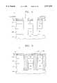
- FIG. 1is a schematic illustration of a known DRAM cell.
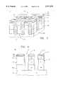
- FIG. 2is a perspective view of the memory array of the present invention.
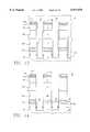
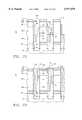
- FIG. 3is a cross-sectional view of a semiconductor wafer undergoing the process of a preferred embodiment.
- FIG. 4shows the wafer of FIG. 3 at a processing step subsequent to that shown in FIG. 3.
- FIG. 5shows the wafer of FIG. 3 at a processing step subsequent to that shown in FIG. 4.
- FIG. 6shows the wafer of FIG. 3 at a processing step subsequent to that shown in FIG. 5.
- FIG. 7shows the wafer of FIG. 3 at a processing step subsequent to that shown in FIG. 6.
- FIG. 8shows the wafer of FIG. 3 at a processing step subsequent to that shown in FIG. 7.
- FIG. 9shows the wafer of FIG. 3 at a processing step subsequent to that shown in FIG. 8.
- FIG. 10shows the wafer of FIG. 3 at a processing step subsequent to that shown in FIG. 9.
- FIG. 11shows the wafer of FIG. 3 at a processing step subsequent to that shown in FIG. 10.
- FIG. 12shows the wafer of FIG. 3 at a processing step subsequent to that shown in FIG. 11.
- FIG. 13shows the wafer of FIG. 3 at a processing step subsequent to that shown in FIG. 12.
- FIG. 14shows the wafer of FIG. 3 at a processing step subsequent to that shown in FIG. 13.
- FIG. 15shows the wafer of FIG. 3 at a processing step subsequent to that shown in FIG. 14.
- FIG. 16shows the wafer of FIG. 3 at a processing step subsequent to that shown in FIG. 15.
- FIG. 17shows the wafer of FIG. 3 at a processing step subsequent to that shown in FIG. 16.
- FIG. 18shows the wafer of FIG. 3 at a processing step subsequent to that shown in FIG. 17.
- FIG. 19shows the wafer of FIG. 3 at a processing step subsequent to that shown in FIG. 18.
- FIG. 20shows the wafer of FIG. 3 at a processing step subsequent to that shown in FIG. 19.
- FIG. 21shows the wafer of FIG. 3 at a processing step subsequent to that shown in FIG. 20.
- FIG. 22shows the wafer of FIG. 3 at a processing step subsequent to that shown in FIG. 21.
- FIG. 23shows the wafer of FIG. 3 at a processing step subsequent to that shown in FIG. 22.
- FIG. 24shows the wafer of FIG. 3 at a processing step subsequent to that shown in FIG. 23.
- FIG. 25shows the wafer of FIG. 3 at a processing step subsequent to that shown in FIG. 24.
- wafer and substrateare to be understood as including silicon-on-insulator (SOI) or silicon-on-sapphire (SOS) technology, doped and undoped semiconductors, epitaxial layers of silicon supported by a base semiconductor foundation, and other semiconductor structures.
- SOIsilicon-on-insulator
- SOSsilicon-on-sapphire
- doped and undoped semiconductorsepitaxial layers of silicon supported by a base semiconductor foundation
- previous process stepsmay have been utilized to form regions or junctions in the base semiconductor structure or foundation.
- the semiconductorneed not be silicon-based, but could be based on silicon-germanium, germanium, or gallium arsenide. The following detailed description is, therefore, not to be taken in a limiting sense, and the scope of the present invention is defined by the appended claims.
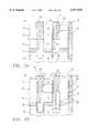
- the device array 40is comprised of a plurality of trench DRAM cells 42 formed on a substrate 60, where the DRAM cells 42 are separated from each other by oxide isolation layers 62.
- Each DRAM cell 42comprises two components, a vertical transistor 46, and a trench capacitor 44 located beneath the transistor 46.
- the transistor 46forms a vertical stack of three doped silicon layers resting on top of the isolation layer 62.
- An exemplary n-channel deviceas illustrated in FIG. 2, would be formed using a substrate 60 of a first conductivity type, e.g., p+, a drain 70 of a second conductivity type (n+), a lightly-doped body region 72 of a first conductivity type (p-), and a source 74 of a second conductivity type (n+). If a p-channel device were desired, the doping types and levels of these elements would be adjusted as is known in the art.
- the capacitor 44comprises a polysilicon electrode 80, which for exemplary purposes is of a second conductivity type (n+), and a dielectric 82, which may be any suitable dielectric material such as oxide, ON (oxide-nitride), or ONO (oxide-nitri-deoxide).
- a polysilicon electrode 80which for exemplary purposes is of a second conductivity type (n+)
- a dielectric 82which may be any suitable dielectric material such as oxide, ON (oxide-nitride), or ONO (oxide-nitri-deoxide).
- the region of the substrate 60 underlying the electrode 80acts as a capacitor plate.
- the transistor 46is a MOSFET (metal-oxide-semiconductor FET) device having four contacts to other portions of the cell 42 or array 40.
- MOSFETmetal-oxide-semiconductor FET
- the drain 70 of the transistor 46is in contact with the capacitor electrode 80.
- a conductive bit line 50 formed of polysilicon doped to a second conductivity type (n+)is formed so that it contacts the source 74 of each transistor 46 of a particular column in th e array 40.
- an active word line 48 of a conductive material such as doped polysilicon of a second conductivity type (n+)is formed to act as the gate of each transistor 46, and to electrically connect all of the cells 42 of a given row in the array 40.
- a thin oxide layer 132is present between the word line 48 and the body 72 of each transistor 46.
- a body line 76 of a conductive material such as doped polysilicon of a first conductivity type (p+)is formed to contact the body 72 of each transistor 46 in a given row. The presence of the body line 76 serves to avoid floating body threshold voltage instabilities.
- the device array 40is manufactured through a process described as following, and illustrated by FIGS. 3 through 25.
- dimensionsare suggested which are suitable for 0.2 micron critical dimension technology, and it should be understood that dimensions should be scaled accordingly for other critical dimension sizes.
- a substrate 60which may be an y of the types of substrate described above, is selected as the base for the device array 40.
- the substrate 60will be described as a silicon substrate, and the following process should be modified as appropriate and as known in the art if a non-silicon substrate is used.
- the substrate 60may be doped or undoped, but a p+type doped wafer is preferred.
- n-wells(not shown) are implanted.
- the level of doping in the n-wellsmay vary but should be of comparable or greater strength than the doping level of the substrate 60.
- the first step in the processis to form the device layers 100, 102, 104.
- the device layers 100, 102, 104are formed of doped epitaxial silicon by known methods of epitaxial growth, such as vapor phase, liquid phase, or solid phase epitaxy. If a silicon substrate 60 is used, then vapor phase epitaxy is preferred, and if a Group III-V compound substrate, e.g., gallium arsenide or indium phosphate, is used, liquid phase epitaxy is preferred.
- the first device layer 100should be a doped silicon layer of a second conductivity type (n+) approximately 0.4 microns thick
- the second device layer 102should be a lightly-doped silicon layer of a first conductivity type (p-) approximately 0.35 microns thick
- the third device layer 104should be a doped silicon layer of a second conductivity type (n+) approximately 0.2 microns thick.
- an oxide pad 106 approximately 10 nm thick, and a first nitride pad 108 approximately 100 nm thickare formed on top of the third device layer 104 by chemical vapor deposition (CVD) or other suitable means.
- a photoresist and maskare then applied over the first nitride pad 108, and photolithographic techniques are used to define a set of parallel columns on the array surface.
- a directional etching processsuch as plasma etching or reactive ion etching (RIE) is used to etch through the pad layers 106, 108 and the device layers 100, 102, 104 and into the substrate 60 to form a first set of trenches 110, as depicted in FIG. 5.
- the trenches 110should be approximately 1.05 microns deep.
- the first set of trenches 110is filled with silicon oxide by CVD or other suitable process to form a first set of silicon oxide bars 112, as shown in FIG. 6.
- the device array 40is then planarized by any suitable means, such as chemical-mechanical polishing (CMP), stopping on the first nitride pad 108.
- CMPchemical-mechanical polishing
- a second nitride pad 114is then deposited, preferably by CVD, to a thickness of about 60 to 100 nm.
- the device array 40now appears as shown in FIG. 6.
- FIG. 7illustrates the next step in the process, in which a resist and mask (not shown) are applied, and photolithography is used to define a second set of trenches 116 orthogonal to the first set of silicon oxide bars 112.
- the nitride pads 108, 114, the oxide pad 106, and the exposed device layers 100, 102, 104are etched out by a directional etching process such as RIE to define the second set of trenches 116.
- Etchingis continued down to the level of the substrate 60, and the second set of trenches 116 should be approximately 0.95 microns deep.
- the resistis then removed.
- the second set of trenches 116is defined by a set of device islands 118, which will be transformed into individual DRAM cells by the fabrication process described herein.
- a first nitride film 120is now formed on the sides of the second set of trenches 116 by depositing a layer of CVD nitride and directionally etching to remove excess nitride from horizontal surfaces.
- the first nitride film 120which is about 10 nm thick, acts as an oxidation and etching barrier during subsequent steps of the fabrication process. Isotropic etching such as RIE is then performed to deepen the second set of trenches 116 an additional 0.1 microns and undercut the device island resulting in the structure shown in FIG. 9.
- Thermal oxidationis then performed to create an isolation layer 62 under and between the device islands 118, as depicted by FIG. 10.
- the substrate 60is thermally oxidized by a suitable process as known in the art, such as by heating the wafer in a standard silicon processing furnace at a temperature of approximately 900 to 1100 degrees Celsius in a wet ambient.
- the oxidation timeis selected to produce an isolation layer 62, at least approximately 0.1 microns thick under the device islands 118.
- FIG. 11shows the next step in the process, in which an anisotropic etch such as RIE is performed to deepen the second set of trenches 116 through the isolation layer 62 and into the substrate 60 to the depth desired for the trench capacitors.
- an anisotropic etchsuch as RIE
- a capacitor dielectric layer 82is now formed inside the second set of trenches 116 on the sides of the device islands 118 and the bottom of the trenches 116.
- the dielectric layer 82may be oxide, ON, or ONO, and is preferably formed by CVD and/or thermal oxidation.
- the second set of trenches 116are filled with a polysilicon layer 80 of a second conductivity type (n+) by CVD or other suitable means, as shown in FIG. 13.
- the polysilicon layer 80is then etched back to a level approximately 1 micron below the second nitride pad 114, as shown in FIG. 14.
- the capacitor dielectric on exposed sidewalls 82is then removed by isotropic etching.
- the second set of trenches 116are then re -filled with polysilicon of a second conductivity type (n+) by CVD.
- the polysiliconis then etched back to a level approximately 0.55 microns below the second nitride pad 114 to form a capacitor electrode 80, depicted in FIG. 15.
- FIG. 16illustrates the next step of the process in which the exposed segments of oxide bars 112 are etched back by ⁇ 0.4 ⁇ m followed by the deposition of a nitride film 122 on the sides of the second set of trenches 116.
- the film 122which is about 10 nm thick, is formed by depositing a layer of CVD nitride and directionally etching to remove excess nitride from horizontal surfaces.
- the second nitride film 122acts as an oxidation barrier during the next step of the process.
- Thermal oxidation of the capacitor electrode 80is now performed by methods known in the art to create a first oxide layer 124 approximately 100 nm thick on top of the electrode 80 in the second set of trenches 116.
- the second nitride film 122is then stripped from the sides of the device islands 118 and remaining segments of oxide 112 in trenches 116, preferably by isotropic etching with a nitride etchant such as phosphoric acid, to form the structure shown in FIG. 17.
- FIG. 18depicts the following step of the process where polysilicon of a first conductivity type (p+) is deposited by CVD or other suitable means in the second set of trenches 116 to a thickness of approximately 70 nm.
- a directional etchsuch as RIE is performed so that no polysilicon remains on the horizontal surfaces of the array 40, and the etch is continued to recess the top of the polysilicon to at least 0.2 microns below the bottom of the oxide pad 106.
- the resultant first and second body lines 76, 78are shown in FIG. 18.
- a conformal film 126 of nitride or other suitable materialis now formed over the first and second body lines 76, 78, as shown in FIG. 19.
- the conformal film 126is approximately 10 nm thick, and is formed by CVD or other suitable methods.
- a photoresist and maskare applied, and photolithography is used to define a third set of trenches 128 inside the second set of trenches 116.
- the exposed conformal film 126is etched off by an isotropic etch, and then a directional etch is performed to remove the second body line 78.
- Directional etchingis continued to remove the exposed first oxide layer 124 and the exposed electrode 80 to a depth below the first device layer 100.
- the resistis stripped, and the third set of trenches is filled with silicon oxide by CVD or known methods, as shown in FIG. 21. If desired, the device array 40 may be planarized by CMP or other means at this point.
- the silicon oxideis then etched back to form a second oxide layer 130 at a level approximately 0.6 to 0.7 microns below the level of the oxide pad 106.
- FIG. 22depicts the next step, in which a thin gate oxide layer 132 is formed by thermal oxidation of the exposed side of the device islands 118.
- polysilicon of a second conductivity type (n+)is deposited by CVD or other suitable means in the third set of trenches 128 to a thickness of approximately 70 nm.
- a directional etchsuch as RIE is performed so that no polysilicon remains on the horizontal surfaces of the array 40.
- a resist and mask(not shown) are then applied, and a selective etch is performed to remove excess polysilicon on the body line 76 side of the third set of trenches 128.
- the resultant word line 48is shown in FIG. 22.
- FIG. 24illustrates the next step in the process, in which a dip etch is performed to remove the nitride pads 108, 114 and the oxide pad 106 from the device islands 118.
- the next stepis to form a conductive bit line 50 over the device array 40 so that it contacts the source 74 of each transistor 46 of a particular row in the array 40.
- the bit line 50is formed of doped polysilicon of a second conductivity type (n+), and is deposited by means such as CVD. After deposition, the polysilicon is patterned by photolithography and subsequent etching to form a bit line 50 as shown in FIG. 25 and in FIG. 2. Conventional processing methods may then be used to form contacts and wiring to connect the device array to peripheral circuits, and to form other connections.
- the entire surfacemay then be covered with a passivation layer of, e.g., silicon dioxide, BSG, PSG, or BPSG, which is CMP planarized and etched to provide contact holes which may then be metallized.
- a passivation layere.g., silicon dioxide, BSG, PSG, or BPSG, which is CMP planarized and etched to provide contact holes which may then be metallized.
- Conventional multiple layers of conductors and insulatorsmay also be used to interconnect the structures.
- the present inventionencompasses a trench DRAM cell having an area of 4F 2 or smaller that comprises a vertical transistor located over a trench capacitor.
- decreasing the size of the DRAM cell while maintaining common process steps with peripheral devicesdecreases fabrication costs while increasing array density.
- a high density and high performance arrayis produced by a simplified fabrication process.
Landscapes
- Engineering & Computer Science (AREA)
- Manufacturing & Machinery (AREA)
- Semiconductor Memories (AREA)
Abstract
Description
Claims (42)
Priority Applications (7)
| Application Number | Priority Date | Filing Date | Title |
|---|---|---|---|
| US09/204,072US5977579A (en) | 1998-12-03 | 1998-12-03 | Trench dram cell with vertical device and buried word lines |
| US09/405,091US6395597B2 (en) | 1998-12-03 | 1999-09-27 | Trench DRAM cell with vertical device and buried word lines |
| US10/152,842US6624033B2 (en) | 1998-12-03 | 2002-05-23 | Trench DRAM cell with vertical device and buried word lines |
| US10/640,387US6946700B2 (en) | 1998-12-03 | 2003-08-14 | Trench DRAM cell with vertical device and buried word lines |
| US10/962,657US7488641B2 (en) | 1998-12-03 | 2004-10-13 | Trench DRAM cell with vertical device and buried word lines |
| US12/357,196US7785961B2 (en) | 1998-12-03 | 2009-01-21 | Trench DRAM cell with vertical device and buried word lines |
| US12/848,369US7883962B2 (en) | 1998-12-03 | 2010-08-02 | Trench DRAM cell with vertical device and buried word lines |
Applications Claiming Priority (1)
| Application Number | Priority Date | Filing Date | Title |
|---|---|---|---|
| US09/204,072US5977579A (en) | 1998-12-03 | 1998-12-03 | Trench dram cell with vertical device and buried word lines |
Related Child Applications (1)
| Application Number | Title | Priority Date | Filing Date |
|---|---|---|---|
| US09/405,091DivisionUS6395597B2 (en) | 1998-12-03 | 1999-09-27 | Trench DRAM cell with vertical device and buried word lines |
Publications (1)
| Publication Number | Publication Date |
|---|---|
| US5977579Atrue US5977579A (en) | 1999-11-02 |
Family
ID=22756512
Family Applications (7)
| Application Number | Title | Priority Date | Filing Date |
|---|---|---|---|
| US09/204,072Expired - LifetimeUS5977579A (en) | 1998-12-03 | 1998-12-03 | Trench dram cell with vertical device and buried word lines |
| US09/405,091Expired - LifetimeUS6395597B2 (en) | 1998-12-03 | 1999-09-27 | Trench DRAM cell with vertical device and buried word lines |
| US10/152,842Expired - LifetimeUS6624033B2 (en) | 1998-12-03 | 2002-05-23 | Trench DRAM cell with vertical device and buried word lines |
| US10/640,387Expired - LifetimeUS6946700B2 (en) | 1998-12-03 | 2003-08-14 | Trench DRAM cell with vertical device and buried word lines |
| US10/962,657Expired - Fee RelatedUS7488641B2 (en) | 1998-12-03 | 2004-10-13 | Trench DRAM cell with vertical device and buried word lines |
| US12/357,196Expired - Fee RelatedUS7785961B2 (en) | 1998-12-03 | 2009-01-21 | Trench DRAM cell with vertical device and buried word lines |
| US12/848,369Expired - Fee RelatedUS7883962B2 (en) | 1998-12-03 | 2010-08-02 | Trench DRAM cell with vertical device and buried word lines |
Family Applications After (6)
| Application Number | Title | Priority Date | Filing Date |
|---|---|---|---|
| US09/405,091Expired - LifetimeUS6395597B2 (en) | 1998-12-03 | 1999-09-27 | Trench DRAM cell with vertical device and buried word lines |
| US10/152,842Expired - LifetimeUS6624033B2 (en) | 1998-12-03 | 2002-05-23 | Trench DRAM cell with vertical device and buried word lines |
| US10/640,387Expired - LifetimeUS6946700B2 (en) | 1998-12-03 | 2003-08-14 | Trench DRAM cell with vertical device and buried word lines |
| US10/962,657Expired - Fee RelatedUS7488641B2 (en) | 1998-12-03 | 2004-10-13 | Trench DRAM cell with vertical device and buried word lines |
| US12/357,196Expired - Fee RelatedUS7785961B2 (en) | 1998-12-03 | 2009-01-21 | Trench DRAM cell with vertical device and buried word lines |
| US12/848,369Expired - Fee RelatedUS7883962B2 (en) | 1998-12-03 | 2010-08-02 | Trench DRAM cell with vertical device and buried word lines |
Country Status (1)
| Country | Link |
|---|---|
| US (7) | US5977579A (en) |
Cited By (296)
| Publication number | Priority date | Publication date | Assignee | Title |
|---|---|---|---|---|
| US6229187B1 (en) | 1999-10-20 | 2001-05-08 | Advanced Micro Devices, Inc. | Field effect transistor with non-floating body and method for forming same on a bulk silicon wafer |
| US6245636B1 (en) | 1999-10-20 | 2001-06-12 | Advanced Micro Devices, Inc. | Method of formation of pseudo-SOI structures with direct contact of transistor body to the substrate |
| US6281539B1 (en) | 2000-03-31 | 2001-08-28 | International Business Machines Corporation | Structure and process for 6F2 DT cell having vertical MOSFET and large storage capacitance |
| US6288422B1 (en) | 2000-03-31 | 2001-09-11 | International Business Machines Corporation | Structure and process for fabricating a 6F2 DRAM cell having vertical MOSFET and large trench capacitance |
| US6309924B1 (en) | 2000-06-02 | 2001-10-30 | International Business Machines Corporation | Method of forming self-limiting polysilicon LOCOS for DRAM cell |
| US6339239B1 (en) | 2000-06-23 | 2002-01-15 | International Business Machines Corporation | DRAM cell layout for node capacitance enhancement |
| US6376286B1 (en)* | 1999-10-20 | 2002-04-23 | Advanced Micro Devices, Inc. | Field effect transistor with non-floating body and method for forming same on a bulk silicon wafer |
| US6448610B2 (en) | 2000-03-07 | 2002-09-10 | Infineon Technologies Ag | Memory cell with trench, and method for production thereof |
| US6465852B1 (en) | 1999-10-20 | 2002-10-15 | Advanced Micro Devices, Inc. | Silicon wafer including both bulk and SOI regions and method for forming same on a bulk silicon wafer |
| US6475890B1 (en)* | 2001-02-12 | 2002-11-05 | Advanced Micro Devices, Inc. | Fabrication of a field effect transistor with an upside down T-shaped semiconductor pillar in SOI technology |
| US20030047767A1 (en)* | 2000-06-23 | 2003-03-13 | Infineon Technologies Ag | Integrated circuit configuration having at least one buried circuit element and an insulating layer |
| US20030049910A1 (en)* | 2001-02-15 | 2003-03-13 | Leonard Forbes | Monotonic Dynamic-Static Pseudo-NMOS Logic Circuit |
| US20030075751A1 (en)* | 1998-09-03 | 2003-04-24 | Kao David Y. | Gapped-plate capacitor |
| US6570207B2 (en) | 2000-12-13 | 2003-05-27 | International Business Machines Corporation | Structure and method for creating vertical capacitor and anti-fuse in DRAM process employing vertical array device cell complex |
| US20030224566A1 (en)* | 2002-05-29 | 2003-12-04 | Clampitt Darwin A. | Biasable isolation regions using epitaxially grown silicon between the isolation regions |
| WO2002037542A3 (en)* | 2000-11-03 | 2004-01-08 | Infineon Technologies Corp | Method for trench capacitor dram cell without floating-well effects |
| US6686283B1 (en)* | 1999-02-05 | 2004-02-03 | Texas Instruments Incorporated | Shallow trench isolation planarization using self aligned isotropic etch |
| US6707092B2 (en)* | 2001-07-16 | 2004-03-16 | Masayoshi Sasaki | Semiconductor memory having longitudinal cell structure |
| US6720602B2 (en)* | 2000-07-19 | 2004-04-13 | International Business Machines Corporation | Dynamic random access memory (DRAM) cell with folded bitline vertical transistor and method of producing the same |
| US20050106795A1 (en)* | 2002-08-15 | 2005-05-19 | Tang Sanh D. | Methods of forming field effect transistors and methods of forming field effect transistor gates and gate lines |
| US20050280155A1 (en)* | 2004-06-21 | 2005-12-22 | Sang-Yun Lee | Semiconductor bonding and layer transfer method |
| US20050280154A1 (en)* | 2004-06-21 | 2005-12-22 | Sang-Yun Lee | Semiconductor memory device |
| US20060017088A1 (en)* | 2004-07-20 | 2006-01-26 | Abbott Todd R | DRAM layout with vertical FETS and method of formation |
| US20060043449A1 (en)* | 2004-09-01 | 2006-03-02 | Tang Sanh D | Semiconductor constructions and transistors, and methods of forming semiconductor constructions and transistors |
| US20060081884A1 (en)* | 2004-03-11 | 2006-04-20 | Micron Technology, Inc. | Semiconductor constructions |
| US20060216889A1 (en)* | 2005-03-28 | 2006-09-28 | Promos Technologies Inc. | Memories having a charge storage node at least partially located in a trench in a semiconductor substrate and electrically coupled to a source/drain region formed in the substrate |
| US20060240634A1 (en)* | 2003-09-17 | 2006-10-26 | Tran Luan C | DRAM access transistor and method of formation |
| US20070048942A1 (en)* | 2005-08-30 | 2007-03-01 | Micron Technology, Inc. | Methods of forming field effect transistors on substrates |
| US20070048941A1 (en)* | 2005-09-01 | 2007-03-01 | Micron Technology, Inc. | Transistor gate forming methods and transistor structures |
| US20070262415A1 (en)* | 2006-05-11 | 2007-11-15 | Casey Smith | Recessed antifuse structures and methods of making the same |
| US20070264771A1 (en)* | 2006-05-11 | 2007-11-15 | Venkatesan Ananthan | Dual work function recessed access device and methods of forming |
| US20070262395A1 (en)* | 2006-05-11 | 2007-11-15 | Gibbons Jasper S | Memory cell access devices and methods of making the same |
| US20080099847A1 (en)* | 2005-03-10 | 2008-05-01 | Micron Technology, Inc. | Integrated Circuits and Methods of Forming a Field Effect Transistor |
| US20080166856A1 (en)* | 2005-03-25 | 2008-07-10 | Parekh Kunal R | Methods of Forming Recessed Access Devices Associated With Semiconductor Constructions |
| US20090026559A1 (en)* | 2007-07-23 | 2009-01-29 | Honeywell International Inc. | Boron doped shell for mems device |
| US7488641B2 (en) | 1998-12-03 | 2009-02-10 | Micron Technology, Inc. | Trench DRAM cell with vertical device and buried word lines |
| US20090111241A1 (en)* | 2003-06-24 | 2009-04-30 | Sang-Yun Lee | Wafer bonding method |
| US7557032B2 (en) | 2005-09-01 | 2009-07-07 | Micron Technology, Inc. | Silicided recessed silicon |
| US7566620B2 (en) | 2005-07-25 | 2009-07-28 | Micron Technology, Inc. | DRAM including a vertical surround gate transistor |
| US20090224364A1 (en)* | 2003-06-24 | 2009-09-10 | Oh Choonsik | Semiconductor circuit and method of fabricating the same |
| US7601595B2 (en) | 2005-07-06 | 2009-10-13 | Micron Technology, Inc. | Surround gate access transistors with grown ultra-thin bodies |
| US20090325343A1 (en)* | 2003-06-24 | 2009-12-31 | Sang-Yun Lee | Bonded semiconductor structure and method of fabricating the same |
| US20100038743A1 (en)* | 2003-06-24 | 2010-02-18 | Sang-Yun Lee | Information storage system which includes a bonded semiconductor structure |
| US20100066440A1 (en)* | 2008-09-15 | 2010-03-18 | Micron Technology, Inc. | Transistor with a passive gate and methods of fabricating the same |
| US7696567B2 (en) | 2005-08-31 | 2010-04-13 | Micron Technology, Inc | Semiconductor memory device |
| US7700441B2 (en) | 2006-02-02 | 2010-04-20 | Micron Technology, Inc. | Methods of forming field effect transistors, methods of forming field effect transistor gates, methods of forming integrated circuitry comprising a transistor gate array and circuitry peripheral to the gate array, and methods of forming integrated circuitry comprising a transistor gate array including first gates and second grounded isolation gates |
| US20100118465A1 (en)* | 2004-08-27 | 2010-05-13 | University Of South Florida | Method of Manufacturing Silicon Topological Capacitors |
| US20100133695A1 (en)* | 2003-01-12 | 2010-06-03 | Sang-Yun Lee | Electronic circuit with embedded memory |
| US20100190334A1 (en)* | 2003-06-24 | 2010-07-29 | Sang-Yun Lee | Three-dimensional semiconductor structure and method of manufacturing the same |
| US7772632B2 (en) | 2006-08-21 | 2010-08-10 | Micron Technology, Inc. | Memory arrays and methods of fabricating memory arrays |
| US7824986B2 (en) | 2008-11-05 | 2010-11-02 | Micron Technology, Inc. | Methods of forming a plurality of transistor gates, and methods of forming a plurality of transistor gates having at least two different work functions |
| US20100283094A1 (en)* | 2005-10-10 | 2010-11-11 | Samsung Electronics Co., Ltd. | Semiconductor device having vertical transistor and method of fabricating the same |
| US20110003438A1 (en)* | 2005-03-29 | 2011-01-06 | Sang-Yun Lee | Three-dimensional integrated circuit structure |
| US7867822B2 (en) | 2003-06-24 | 2011-01-11 | Sang-Yun Lee | Semiconductor memory device |
| US20110042734A1 (en)* | 2004-09-01 | 2011-02-24 | Micron Technology, Inc. | Memory cell with a vertically oriented transistor coupled to a digit line and method of forming the same |
| US20110053332A1 (en)* | 2003-06-24 | 2011-03-03 | Sang-Yun Lee | Semiconductor circuit |
| US7935999B2 (en) | 2005-09-01 | 2011-05-03 | Micron Technology, Inc. | Memory device |
| US7939409B2 (en) | 2005-09-01 | 2011-05-10 | Micron Technology, Inc. | Peripheral gate stacks and recessed array gates |
| US7944743B2 (en) | 2006-09-07 | 2011-05-17 | Micron Technology, Inc. | Methods of making a semiconductor memory device |
| US20110143506A1 (en)* | 2009-12-10 | 2011-06-16 | Sang-Yun Lee | Method for fabricating a semiconductor memory device |
| US8058142B2 (en) | 1996-11-04 | 2011-11-15 | Besang Inc. | Bonded semiconductor structure and method of making the same |
| US8101992B2 (en) | 2005-05-13 | 2012-01-24 | Micron Technology, Inc. | Memory array with surrounding gate access transistors and capacitors with global and staggered local bit lines |
| US8203148B2 (en) | 2010-10-11 | 2012-06-19 | Monolithic 3D Inc. | Semiconductor device and structure |
| US8227305B2 (en) | 2005-05-13 | 2012-07-24 | Micron Technology, Inc. | Memory array with ultra-thin etched pillar surround gate access transistors and buried data/bit lines |
| US8237228B2 (en) | 2009-10-12 | 2012-08-07 | Monolithic 3D Inc. | System comprising a semiconductor device and structure |
| US8273610B2 (en) | 2010-11-18 | 2012-09-25 | Monolithic 3D Inc. | Method of constructing a semiconductor device and structure |
| US8294159B2 (en) | 2009-10-12 | 2012-10-23 | Monolithic 3D Inc. | Method for fabrication of a semiconductor device and structure |
| US8362482B2 (en) | 2009-04-14 | 2013-01-29 | Monolithic 3D Inc. | Semiconductor device and structure |
| US8362800B2 (en) | 2010-10-13 | 2013-01-29 | Monolithic 3D Inc. | 3D semiconductor device including field repairable logics |
| US8373230B1 (en) | 2010-10-13 | 2013-02-12 | Monolithic 3D Inc. | Method for fabrication of a semiconductor device and structure |
| US8373439B2 (en) | 2009-04-14 | 2013-02-12 | Monolithic 3D Inc. | 3D semiconductor device |
| US8378715B2 (en) | 2009-04-14 | 2013-02-19 | Monolithic 3D Inc. | Method to construct systems |
| US8379458B1 (en) | 2010-10-13 | 2013-02-19 | Monolithic 3D Inc. | Semiconductor device and structure |
| US8378494B2 (en) | 2009-04-14 | 2013-02-19 | Monolithic 3D Inc. | Method for fabrication of a semiconductor device and structure |
| US8384426B2 (en) | 2009-04-14 | 2013-02-26 | Monolithic 3D Inc. | Semiconductor device and structure |
| US8399920B2 (en) | 2005-07-08 | 2013-03-19 | Werner Juengling | Semiconductor device comprising a transistor gate having multiple vertically oriented sidewalls |
| US8405420B2 (en) | 2009-04-14 | 2013-03-26 | Monolithic 3D Inc. | System comprising a semiconductor device and structure |
| US8427200B2 (en) | 2009-04-14 | 2013-04-23 | Monolithic 3D Inc. | 3D semiconductor device |
| US8440542B2 (en) | 2010-10-11 | 2013-05-14 | Monolithic 3D Inc. | Semiconductor device and structure |
| US8450804B2 (en) | 2011-03-06 | 2013-05-28 | Monolithic 3D Inc. | Semiconductor device and structure for heat removal |
| US8455978B2 (en) | 2010-05-27 | 2013-06-04 | Sang-Yun Lee | Semiconductor circuit structure and method of making the same |
| US8461035B1 (en) | 2010-09-30 | 2013-06-11 | Monolithic 3D Inc. | Method for fabrication of a semiconductor device and structure |
| US8476145B2 (en) | 2010-10-13 | 2013-07-02 | Monolithic 3D Inc. | Method of fabricating a semiconductor device and structure |
| US8492886B2 (en) | 2010-02-16 | 2013-07-23 | Monolithic 3D Inc | 3D integrated circuit with logic |
| US8524560B2 (en)* | 2010-10-08 | 2013-09-03 | Samsung Electronics Co., Ltd. | Method of fabricating semiconductor device with vertical channel transistor |
| US8536023B2 (en) | 2010-11-22 | 2013-09-17 | Monolithic 3D Inc. | Method of manufacturing a semiconductor device and structure |
| US8541819B1 (en) | 2010-12-09 | 2013-09-24 | Monolithic 3D Inc. | Semiconductor device and structure |
| US8551823B2 (en) | 2006-07-17 | 2013-10-08 | Micron Technology, Inc. | Methods of forming lines of capacitorless one transistor DRAM cells, methods of patterning substrates, and methods of forming two conductive lines |
| US8557632B1 (en) | 2012-04-09 | 2013-10-15 | Monolithic 3D Inc. | Method for fabrication of a semiconductor device and structure |
| US8574929B1 (en) | 2012-11-16 | 2013-11-05 | Monolithic 3D Inc. | Method to form a 3D semiconductor device and structure |
| US8581349B1 (en) | 2011-05-02 | 2013-11-12 | Monolithic 3D Inc. | 3D memory semiconductor device and structure |
| US8642416B2 (en) | 2010-07-30 | 2014-02-04 | Monolithic 3D Inc. | Method of forming three dimensional integrated circuit devices using layer transfer technique |
| US8669778B1 (en) | 2009-04-14 | 2014-03-11 | Monolithic 3D Inc. | Method for design and manufacturing of a 3D semiconductor device |
| US8674470B1 (en) | 2012-12-22 | 2014-03-18 | Monolithic 3D Inc. | Semiconductor device and structure |
| US8687399B2 (en) | 2011-10-02 | 2014-04-01 | Monolithic 3D Inc. | Semiconductor device and structure |
| US8686428B1 (en) | 2012-11-16 | 2014-04-01 | Monolithic 3D Inc. | Semiconductor device and structure |
| US8709880B2 (en) | 2010-07-30 | 2014-04-29 | Monolithic 3D Inc | Method for fabrication of a semiconductor device and structure |
| US8723335B2 (en) | 2010-05-20 | 2014-05-13 | Sang-Yun Lee | Semiconductor circuit structure and method of forming the same using a capping layer |
| US8742476B1 (en) | 2012-11-27 | 2014-06-03 | Monolithic 3D Inc. | Semiconductor device and structure |
| US8753913B2 (en) | 2010-10-13 | 2014-06-17 | Monolithic 3D Inc. | Method for fabricating novel semiconductor and optoelectronic devices |
| US8754533B2 (en) | 2009-04-14 | 2014-06-17 | Monolithic 3D Inc. | Monolithic three-dimensional semiconductor device and structure |
| US8803206B1 (en) | 2012-12-29 | 2014-08-12 | Monolithic 3D Inc. | 3D semiconductor device and structure |
| US8901613B2 (en) | 2011-03-06 | 2014-12-02 | Monolithic 3D Inc. | Semiconductor device and structure for heat removal |
| US8902663B1 (en) | 2013-03-11 | 2014-12-02 | Monolithic 3D Inc. | Method of maintaining a memory state |
| US8975670B2 (en) | 2011-03-06 | 2015-03-10 | Monolithic 3D Inc. | Semiconductor device and structure for heat removal |
| US8994404B1 (en) | 2013-03-12 | 2015-03-31 | Monolithic 3D Inc. | Semiconductor device and structure |
| US9000557B2 (en) | 2012-03-17 | 2015-04-07 | Zvi Or-Bach | Semiconductor device and structure |
| US9029173B2 (en) | 2011-10-18 | 2015-05-12 | Monolithic 3D Inc. | Method for fabrication of a semiconductor device and structure |
| US9099526B2 (en) | 2010-02-16 | 2015-08-04 | Monolithic 3D Inc. | Integrated circuit device and structure |
| US9099424B1 (en) | 2012-08-10 | 2015-08-04 | Monolithic 3D Inc. | Semiconductor system, device and structure with heat removal |
| US9117749B1 (en) | 2013-03-15 | 2015-08-25 | Monolithic 3D Inc. | Semiconductor device and structure |
| US9197804B1 (en) | 2011-10-14 | 2015-11-24 | Monolithic 3D Inc. | Semiconductor and optoelectronic devices |
| US9219005B2 (en) | 2011-06-28 | 2015-12-22 | Monolithic 3D Inc. | Semiconductor system and device |
| US9252192B2 (en)* | 2014-06-20 | 2016-02-02 | SK Hynix Inc. | Methods of manufacturing semiconductor devices including a cross point cell array |
| US9287271B2 (en) | 2011-08-23 | 2016-03-15 | Micron Technology, Inc. | Vertical transistor devices, memory arrays, and methods of forming vertical transistor devices |
| US9509313B2 (en) | 2009-04-14 | 2016-11-29 | Monolithic 3D Inc. | 3D semiconductor device |
| US9577642B2 (en) | 2009-04-14 | 2017-02-21 | Monolithic 3D Inc. | Method to form a 3D semiconductor device |
| WO2017091780A1 (en)* | 2015-11-26 | 2017-06-01 | Fu-Chang Hsu | 3d cross-point array and process flows |
| US9711407B2 (en) | 2009-04-14 | 2017-07-18 | Monolithic 3D Inc. | Method of manufacturing a three dimensional integrated circuit by transfer of a mono-crystalline layer |
| US9871034B1 (en) | 2012-12-29 | 2018-01-16 | Monolithic 3D Inc. | Semiconductor device and structure |
| US9953925B2 (en) | 2011-06-28 | 2018-04-24 | Monolithic 3D Inc. | Semiconductor system and device |
| US10043781B2 (en) | 2009-10-12 | 2018-08-07 | Monolithic 3D Inc. | 3D semiconductor device and structure |
| US10115663B2 (en) | 2012-12-29 | 2018-10-30 | Monolithic 3D Inc. | 3D semiconductor device and structure |
| US10127344B2 (en) | 2013-04-15 | 2018-11-13 | Monolithic 3D Inc. | Automation for monolithic 3D devices |
| US10157909B2 (en) | 2009-10-12 | 2018-12-18 | Monolithic 3D Inc. | 3D semiconductor device and structure |
| US10217667B2 (en) | 2011-06-28 | 2019-02-26 | Monolithic 3D Inc. | 3D semiconductor device, fabrication method and system |
| US10224279B2 (en) | 2013-03-15 | 2019-03-05 | Monolithic 3D Inc. | Semiconductor device and structure |
| US10290682B2 (en) | 2010-10-11 | 2019-05-14 | Monolithic 3D Inc. | 3D IC semiconductor device and structure with stacked memory |
| US10297586B2 (en) | 2015-03-09 | 2019-05-21 | Monolithic 3D Inc. | Methods for processing a 3D semiconductor device |
| US10325651B2 (en) | 2013-03-11 | 2019-06-18 | Monolithic 3D Inc. | 3D semiconductor device with stacked memory |
| US10354995B2 (en) | 2009-10-12 | 2019-07-16 | Monolithic 3D Inc. | Semiconductor memory device and structure |
| US10366970B2 (en) | 2009-10-12 | 2019-07-30 | Monolithic 3D Inc. | 3D semiconductor device and structure |
| US10381328B2 (en) | 2015-04-19 | 2019-08-13 | Monolithic 3D Inc. | Semiconductor device and structure |
| US10388863B2 (en) | 2009-10-12 | 2019-08-20 | Monolithic 3D Inc. | 3D memory device and structure |
| US10388568B2 (en) | 2011-06-28 | 2019-08-20 | Monolithic 3D Inc. | 3D semiconductor device and system |
| US10418369B2 (en) | 2015-10-24 | 2019-09-17 | Monolithic 3D Inc. | Multi-level semiconductor memory device and structure |
| US10497713B2 (en) | 2010-11-18 | 2019-12-03 | Monolithic 3D Inc. | 3D semiconductor memory device and structure |
| US10515981B2 (en) | 2015-09-21 | 2019-12-24 | Monolithic 3D Inc. | Multilevel semiconductor device and structure with memory |
| US10515801B2 (en) | 2007-06-04 | 2019-12-24 | Micron Technology, Inc. | Pitch multiplication using self-assembling materials |
| US10522225B1 (en) | 2015-10-02 | 2019-12-31 | Monolithic 3D Inc. | Semiconductor device with non-volatile memory |
| US10600657B2 (en) | 2012-12-29 | 2020-03-24 | Monolithic 3D Inc | 3D semiconductor device and structure |
| US10600888B2 (en) | 2012-04-09 | 2020-03-24 | Monolithic 3D Inc. | 3D semiconductor device |
| US10651054B2 (en) | 2012-12-29 | 2020-05-12 | Monolithic 3D Inc. | 3D semiconductor device and structure |
| US10679977B2 (en) | 2010-10-13 | 2020-06-09 | Monolithic 3D Inc. | 3D microdisplay device and structure |
| TWI708320B (en)* | 2019-10-29 | 2020-10-21 | 南亞科技股份有限公司 | Semiconductor structure and method of forming the same |
| US10825779B2 (en) | 2015-04-19 | 2020-11-03 | Monolithic 3D Inc. | 3D semiconductor device and structure |
| US10833108B2 (en) | 2010-10-13 | 2020-11-10 | Monolithic 3D Inc. | 3D microdisplay device and structure |
| US10840239B2 (en) | 2014-08-26 | 2020-11-17 | Monolithic 3D Inc. | 3D semiconductor device and structure |
| US10847540B2 (en) | 2015-10-24 | 2020-11-24 | Monolithic 3D Inc. | 3D semiconductor memory device and structure |
| US10892169B2 (en) | 2012-12-29 | 2021-01-12 | Monolithic 3D Inc. | 3D semiconductor device and structure |
| US10892016B1 (en) | 2019-04-08 | 2021-01-12 | Monolithic 3D Inc. | 3D memory semiconductor devices and structures |
| US10896931B1 (en) | 2010-10-11 | 2021-01-19 | Monolithic 3D Inc. | 3D semiconductor device and structure |
| US10903089B1 (en) | 2012-12-29 | 2021-01-26 | Monolithic 3D Inc. | 3D semiconductor device and structure |
| US10910364B2 (en) | 2009-10-12 | 2021-02-02 | Monolitaic 3D Inc. | 3D semiconductor device |
| US10943934B2 (en) | 2010-10-13 | 2021-03-09 | Monolithic 3D Inc. | Multilevel semiconductor device and structure |
| CN112585752A (en)* | 2018-09-05 | 2021-03-30 | 东京毅力科创株式会社 | Power distribution network for 3D logic and memory |
| US10978501B1 (en) | 2010-10-13 | 2021-04-13 | Monolithic 3D Inc. | Multilevel semiconductor device and structure with waveguides |
| US10998374B1 (en) | 2010-10-13 | 2021-05-04 | Monolithic 3D Inc. | Multilevel semiconductor device and structure |
| US11004719B1 (en) | 2010-11-18 | 2021-05-11 | Monolithic 3D Inc. | Methods for producing a 3D semiconductor memory device and structure |
| US11004694B1 (en) | 2012-12-29 | 2021-05-11 | Monolithic 3D Inc. | 3D semiconductor device and structure |
| US11011507B1 (en) | 2015-04-19 | 2021-05-18 | Monolithic 3D Inc. | 3D semiconductor device and structure |
| US11018116B2 (en) | 2012-12-22 | 2021-05-25 | Monolithic 3D Inc. | Method to form a 3D semiconductor device and structure |
| US11018133B2 (en) | 2009-10-12 | 2021-05-25 | Monolithic 3D Inc. | 3D integrated circuit |
| US11018042B1 (en) | 2010-11-18 | 2021-05-25 | Monolithic 3D Inc. | 3D semiconductor memory device and structure |
| US11018156B2 (en) | 2019-04-08 | 2021-05-25 | Monolithic 3D Inc. | 3D memory semiconductor devices and structures |
| US11018191B1 (en) | 2010-10-11 | 2021-05-25 | Monolithic 3D Inc. | 3D semiconductor device and structure |
| US11024673B1 (en) | 2010-10-11 | 2021-06-01 | Monolithic 3D Inc. | 3D semiconductor device and structure |
| US11031394B1 (en) | 2014-01-28 | 2021-06-08 | Monolithic 3D Inc. | 3D semiconductor device and structure |
| US11030371B2 (en) | 2013-04-15 | 2021-06-08 | Monolithic 3D Inc. | Automation for monolithic 3D devices |
| US11031275B2 (en) | 2010-11-18 | 2021-06-08 | Monolithic 3D Inc. | 3D semiconductor device and structure with memory |
| US11043523B1 (en) | 2010-10-13 | 2021-06-22 | Monolithic 3D Inc. | Multilevel semiconductor device and structure with image sensors |
| US11056468B1 (en) | 2015-04-19 | 2021-07-06 | Monolithic 3D Inc. | 3D semiconductor device and structure |
| US11063024B1 (en) | 2012-12-22 | 2021-07-13 | Monlithic 3D Inc. | Method to form a 3D semiconductor device and structure |
| US11063071B1 (en) | 2010-10-13 | 2021-07-13 | Monolithic 3D Inc. | Multilevel semiconductor device and structure with waveguides |
| US11088050B2 (en) | 2012-04-09 | 2021-08-10 | Monolithic 3D Inc. | 3D semiconductor device with isolation layers |
| US11088130B2 (en) | 2014-01-28 | 2021-08-10 | Monolithic 3D Inc. | 3D semiconductor device and structure |
| US11087995B1 (en) | 2012-12-29 | 2021-08-10 | Monolithic 3D Inc. | 3D semiconductor device and structure |
| US11094576B1 (en) | 2010-11-18 | 2021-08-17 | Monolithic 3D Inc. | Methods for producing a 3D semiconductor memory device and structure |
| US11107721B2 (en) | 2010-11-18 | 2021-08-31 | Monolithic 3D Inc. | 3D semiconductor device and structure with NAND logic |
| US11107808B1 (en) | 2014-01-28 | 2021-08-31 | Monolithic 3D Inc. | 3D semiconductor device and structure |
| US11114464B2 (en) | 2015-10-24 | 2021-09-07 | Monolithic 3D Inc. | 3D semiconductor device and structure |
| US11114427B2 (en) | 2015-11-07 | 2021-09-07 | Monolithic 3D Inc. | 3D semiconductor processor and memory device and structure |
| US11121021B2 (en) | 2010-11-18 | 2021-09-14 | Monolithic 3D Inc. | 3D semiconductor device and structure |
| US11133344B2 (en) | 2010-10-13 | 2021-09-28 | Monolithic 3D Inc. | Multilevel semiconductor device and structure with image sensors |
| US11158652B1 (en) | 2019-04-08 | 2021-10-26 | Monolithic 3D Inc. | 3D memory semiconductor devices and structures |
| US11158674B2 (en) | 2010-10-11 | 2021-10-26 | Monolithic 3D Inc. | Method to produce a 3D semiconductor device and structure |
| US11163112B2 (en) | 2010-10-13 | 2021-11-02 | Monolithic 3D Inc. | Multilevel semiconductor device and structure with electromagnetic modulators |
| US11164770B1 (en) | 2010-11-18 | 2021-11-02 | Monolithic 3D Inc. | Method for producing a 3D semiconductor memory device and structure |
| US11164811B2 (en) | 2012-04-09 | 2021-11-02 | Monolithic 3D Inc. | 3D semiconductor device with isolation layers and oxide-to-oxide bonding |
| US11164898B2 (en) | 2010-10-13 | 2021-11-02 | Monolithic 3D Inc. | Multilevel semiconductor device and structure |
| US11177140B2 (en) | 2012-12-29 | 2021-11-16 | Monolithic 3D Inc. | 3D semiconductor device and structure |
| US11211279B2 (en) | 2010-11-18 | 2021-12-28 | Monolithic 3D Inc. | Method for processing a 3D integrated circuit and structure |
| US11217565B2 (en) | 2012-12-22 | 2022-01-04 | Monolithic 3D Inc. | Method to form a 3D semiconductor device and structure |
| US11227897B2 (en) | 2010-10-11 | 2022-01-18 | Monolithic 3D Inc. | Method for producing a 3D semiconductor memory device and structure |
| US11251149B2 (en) | 2016-10-10 | 2022-02-15 | Monolithic 3D Inc. | 3D memory device and structure |
| US11257867B1 (en) | 2010-10-11 | 2022-02-22 | Monolithic 3D Inc. | 3D semiconductor device and structure with oxide bonds |
| CN114121958A (en)* | 2020-08-25 | 2022-03-01 | 南亚科技股份有限公司 | Memory element and method of forming the same |
| US11270055B1 (en) | 2013-04-15 | 2022-03-08 | Monolithic 3D Inc. | Automation for monolithic 3D devices |
| US11296115B1 (en) | 2015-10-24 | 2022-04-05 | Monolithic 3D Inc. | 3D semiconductor device and structure |
| US11296106B2 (en) | 2019-04-08 | 2022-04-05 | Monolithic 3D Inc. | 3D memory semiconductor devices and structures |
| US11309292B2 (en) | 2012-12-22 | 2022-04-19 | Monolithic 3D Inc. | 3D semiconductor device and structure with metal layers |
| US11315980B1 (en) | 2010-10-11 | 2022-04-26 | Monolithic 3D Inc. | 3D semiconductor device and structure with transistors |
| US11329059B1 (en) | 2016-10-10 | 2022-05-10 | Monolithic 3D Inc. | 3D memory devices and structures with thinned single crystal substrates |
| US11327227B2 (en) | 2010-10-13 | 2022-05-10 | Monolithic 3D Inc. | Multilevel semiconductor device and structure with electromagnetic modulators |
| US11341309B1 (en) | 2013-04-15 | 2022-05-24 | Monolithic 3D Inc. | Automation for monolithic 3D devices |
| US11355380B2 (en) | 2010-11-18 | 2022-06-07 | Monolithic 3D Inc. | Methods for producing 3D semiconductor memory device and structure utilizing alignment marks |
| US11355381B2 (en) | 2010-11-18 | 2022-06-07 | Monolithic 3D Inc. | 3D semiconductor memory device and structure |
| US11374118B2 (en) | 2009-10-12 | 2022-06-28 | Monolithic 3D Inc. | Method to form a 3D integrated circuit |
| US11398569B2 (en) | 2013-03-12 | 2022-07-26 | Monolithic 3D Inc. | 3D semiconductor device and structure |
| US11404466B2 (en) | 2010-10-13 | 2022-08-02 | Monolithic 3D Inc. | Multilevel semiconductor device and structure with image sensors |
| US11410912B2 (en) | 2012-04-09 | 2022-08-09 | Monolithic 3D Inc. | 3D semiconductor device with vias and isolation layers |
| US11430668B2 (en) | 2012-12-29 | 2022-08-30 | Monolithic 3D Inc. | 3D semiconductor device and structure with bonding |
| US11430667B2 (en) | 2012-12-29 | 2022-08-30 | Monolithic 3D Inc. | 3D semiconductor device and structure with bonding |
| CN114975616A (en)* | 2021-02-22 | 2022-08-30 | 爱思开海力士有限公司 | Memory cell and semiconductor memory device having the same |
| US11437368B2 (en) | 2010-10-13 | 2022-09-06 | Monolithic 3D Inc. | Multilevel semiconductor device and structure with oxide bonding |
| US11443971B2 (en) | 2010-11-18 | 2022-09-13 | Monolithic 3D Inc. | 3D semiconductor device and structure with memory |
| US11469271B2 (en) | 2010-10-11 | 2022-10-11 | Monolithic 3D Inc. | Method to produce 3D semiconductor devices and structures with memory |
| US11476181B1 (en) | 2012-04-09 | 2022-10-18 | Monolithic 3D Inc. | 3D semiconductor device and structure with metal layers |
| US11482438B2 (en) | 2010-11-18 | 2022-10-25 | Monolithic 3D Inc. | Methods for producing a 3D semiconductor memory device and structure |
| US11482439B2 (en) | 2010-11-18 | 2022-10-25 | Monolithic 3D Inc. | Methods for producing a 3D semiconductor memory device comprising charge trap junction-less transistors |
| US11482440B2 (en) | 2010-12-16 | 2022-10-25 | Monolithic 3D Inc. | 3D semiconductor device and structure with a built-in test circuit for repairing faulty circuits |
| US11487928B2 (en) | 2013-04-15 | 2022-11-01 | Monolithic 3D Inc. | Automation for monolithic 3D devices |
| US11495484B2 (en) | 2010-11-18 | 2022-11-08 | Monolithic 3D Inc. | 3D semiconductor devices and structures with at least two single-crystal layers |
| US11508605B2 (en) | 2010-11-18 | 2022-11-22 | Monolithic 3D Inc. | 3D semiconductor memory device and structure |
| US11521888B2 (en) | 2010-11-18 | 2022-12-06 | Monolithic 3D Inc. | 3D semiconductor device and structure with high-k metal gate transistors |
| US11569117B2 (en) | 2010-11-18 | 2023-01-31 | Monolithic 3D Inc. | 3D semiconductor device and structure with single-crystal layers |
| US11574109B1 (en) | 2013-04-15 | 2023-02-07 | Monolithic 3D Inc | Automation methods for 3D integrated circuits and devices |
| US11594473B2 (en) | 2012-04-09 | 2023-02-28 | Monolithic 3D Inc. | 3D semiconductor device and structure with metal layers and a connective path |
| US11600667B1 (en) | 2010-10-11 | 2023-03-07 | Monolithic 3D Inc. | Method to produce 3D semiconductor devices and structures with memory |
| US11605663B2 (en) | 2010-10-13 | 2023-03-14 | Monolithic 3D Inc. | Multilevel semiconductor device and structure with image sensors and wafer bonding |
| US11610802B2 (en) | 2010-11-18 | 2023-03-21 | Monolithic 3D Inc. | Method for producing a 3D semiconductor device and structure with single crystal transistors and metal gate electrodes |
| US11615977B2 (en) | 2010-11-18 | 2023-03-28 | Monolithic 3D Inc. | 3D semiconductor memory device and structure |
| US11616004B1 (en) | 2012-04-09 | 2023-03-28 | Monolithic 3D Inc. | 3D semiconductor device and structure with metal layers and a connective path |
| US11694944B1 (en) | 2012-04-09 | 2023-07-04 | Monolithic 3D Inc. | 3D semiconductor device and structure with metal layers and a connective path |
| US11694922B2 (en) | 2010-10-13 | 2023-07-04 | Monolithic 3D Inc. | Multilevel semiconductor device and structure with oxide bonding |
| US11711928B2 (en) | 2016-10-10 | 2023-07-25 | Monolithic 3D Inc. | 3D memory devices and structures with control circuits |
| US11720736B2 (en) | 2013-04-15 | 2023-08-08 | Monolithic 3D Inc. | Automation methods for 3D integrated circuits and devices |
| US11735501B1 (en) | 2012-04-09 | 2023-08-22 | Monolithic 3D Inc. | 3D semiconductor device and structure with metal layers and a connective path |
| US11735462B2 (en) | 2010-11-18 | 2023-08-22 | Monolithic 3D Inc. | 3D semiconductor device and structure with single-crystal layers |
| US11763864B2 (en) | 2019-04-08 | 2023-09-19 | Monolithic 3D Inc. | 3D memory semiconductor devices and structures with bit-line pillars |
| US11784169B2 (en) | 2012-12-22 | 2023-10-10 | Monolithic 3D Inc. | 3D semiconductor device and structure with metal layers |
| US11784082B2 (en) | 2010-11-18 | 2023-10-10 | Monolithic 3D Inc. | 3D semiconductor device and structure with bonding |
| US11804396B2 (en) | 2010-11-18 | 2023-10-31 | Monolithic 3D Inc. | Methods for producing a 3D semiconductor device and structure with memory cells and multiple metal layers |
| US11812620B2 (en) | 2016-10-10 | 2023-11-07 | Monolithic 3D Inc. | 3D DRAM memory devices and structures with control circuits |
| US11818877B2 (en) | 2020-11-02 | 2023-11-14 | Applied Materials, Inc. | Three-dimensional dynamic random access memory (DRAM) and methods of forming the same |
| US11854857B1 (en) | 2010-11-18 | 2023-12-26 | Monolithic 3D Inc. | Methods for producing a 3D semiconductor device and structure with memory cells and multiple metal layers |
| US11855100B2 (en) | 2010-10-13 | 2023-12-26 | Monolithic 3D Inc. | Multilevel semiconductor device and structure with oxide bonding |
| US11855114B2 (en) | 2010-10-13 | 2023-12-26 | Monolithic 3D Inc. | Multilevel semiconductor device and structure with image sensors and wafer bonding |
| US11862503B2 (en) | 2010-11-18 | 2024-01-02 | Monolithic 3D Inc. | Method for producing a 3D semiconductor device and structure with memory cells and multiple metal layers |
| US11869915B2 (en) | 2010-10-13 | 2024-01-09 | Monolithic 3D Inc. | Multilevel semiconductor device and structure with image sensors and wafer bonding |
| US11869591B2 (en) | 2016-10-10 | 2024-01-09 | Monolithic 3D Inc. | 3D memory devices and structures with control circuits |
| US11869965B2 (en) | 2013-03-11 | 2024-01-09 | Monolithic 3D Inc. | 3D semiconductor device and structure with metal layers and memory cells |
| US11881443B2 (en) | 2012-04-09 | 2024-01-23 | Monolithic 3D Inc. | 3D semiconductor device and structure with metal layers and a connective path |
| US11901210B2 (en) | 2010-11-18 | 2024-02-13 | Monolithic 3D Inc. | 3D semiconductor device and structure with memory |
| US11916045B2 (en) | 2012-12-22 | 2024-02-27 | Monolithic 3D Inc. | 3D semiconductor device and structure with metal layers |
| US11923374B2 (en) | 2013-03-12 | 2024-03-05 | Monolithic 3D Inc. | 3D semiconductor device and structure with metal layers |
| US11923230B1 (en) | 2010-11-18 | 2024-03-05 | Monolithic 3D Inc. | 3D semiconductor device and structure with bonding |
| US11929372B2 (en) | 2010-10-13 | 2024-03-12 | Monolithic 3D Inc. | Multilevel semiconductor device and structure with image sensors and wafer bonding |
| US11930648B1 (en) | 2016-10-10 | 2024-03-12 | Monolithic 3D Inc. | 3D memory devices and structures with metal layers |
| US11937422B2 (en) | 2015-11-07 | 2024-03-19 | Monolithic 3D Inc. | Semiconductor memory device and structure |
| US11935949B1 (en) | 2013-03-11 | 2024-03-19 | Monolithic 3D Inc. | 3D semiconductor device and structure with metal layers and memory cells |
| US11956952B2 (en) | 2015-08-23 | 2024-04-09 | Monolithic 3D Inc. | Semiconductor memory device and structure |
| US11961827B1 (en) | 2012-12-22 | 2024-04-16 | Monolithic 3D Inc. | 3D semiconductor device and structure with metal layers |
| US11967583B2 (en) | 2012-12-22 | 2024-04-23 | Monolithic 3D Inc. | 3D semiconductor device and structure with metal layers |
| US11978731B2 (en) | 2015-09-21 | 2024-05-07 | Monolithic 3D Inc. | Method to produce a multi-level semiconductor memory device and structure |
| US11984438B2 (en) | 2010-10-13 | 2024-05-14 | Monolithic 3D Inc. | Multilevel semiconductor device and structure with oxide bonding |
| US11984445B2 (en) | 2009-10-12 | 2024-05-14 | Monolithic 3D Inc. | 3D semiconductor devices and structures with metal layers |
| US11991884B1 (en) | 2015-10-24 | 2024-05-21 | Monolithic 3D Inc. | 3D semiconductor device and structure with logic and memory |
| US12016181B2 (en) | 2015-10-24 | 2024-06-18 | Monolithic 3D Inc. | 3D semiconductor device and structure with logic and memory |
| US12027518B1 (en) | 2009-10-12 | 2024-07-02 | Monolithic 3D Inc. | 3D semiconductor devices and structures with metal layers |
| US12033884B2 (en) | 2010-11-18 | 2024-07-09 | Monolithic 3D Inc. | Methods for producing a 3D semiconductor device and structure with memory cells and multiple metal layers |
| US12035531B2 (en) | 2015-10-24 | 2024-07-09 | Monolithic 3D Inc. | 3D semiconductor device and structure with logic and memory |
| US12051674B2 (en) | 2012-12-22 | 2024-07-30 | Monolithic 3D Inc. | 3D semiconductor device and structure with metal layers |
| US12068187B2 (en) | 2010-11-18 | 2024-08-20 | Monolithic 3D Inc. | 3D semiconductor device and structure with bonding and DRAM memory cells |
| US12080743B2 (en) | 2010-10-13 | 2024-09-03 | Monolithic 3D Inc. | Multilevel semiconductor device and structure with image sensors and wafer bonding |
| US12087669B1 (en)* | 2023-08-14 | 2024-09-10 | Samsung Electronics Co., Ltd. | Integrated circuit devices including discharging path and methods of forming the same |
| US12094965B2 (en) | 2013-03-11 | 2024-09-17 | Monolithic 3D Inc. | 3D semiconductor device and structure with metal layers and memory cells |
| US12094892B2 (en) | 2010-10-13 | 2024-09-17 | Monolithic 3D Inc. | 3D micro display device and structure |
| US12094829B2 (en) | 2014-01-28 | 2024-09-17 | Monolithic 3D Inc. | 3D semiconductor device and structure |
| US12100611B2 (en) | 2010-11-18 | 2024-09-24 | Monolithic 3D Inc. | Methods for producing a 3D semiconductor device and structure with memory cells and multiple metal layers |
| US12100646B2 (en) | 2013-03-12 | 2024-09-24 | Monolithic 3D Inc. | 3D semiconductor device and structure with metal layers |
| US12100658B2 (en) | 2015-09-21 | 2024-09-24 | Monolithic 3D Inc. | Method to produce a 3D multilayer semiconductor device and structure |
| US12120880B1 (en) | 2015-10-24 | 2024-10-15 | Monolithic 3D Inc. | 3D semiconductor device and structure with logic and memory |
| US12125737B1 (en) | 2010-11-18 | 2024-10-22 | Monolithic 3D Inc. | 3D semiconductor device and structure with metal layers and memory cells |
| US12136562B2 (en) | 2010-11-18 | 2024-11-05 | Monolithic 3D Inc. | 3D semiconductor device and structure with single-crystal layers |
| US12144190B2 (en) | 2010-11-18 | 2024-11-12 | Monolithic 3D Inc. | 3D semiconductor device and structure with bonding and memory cells preliminary class |
| US12154817B1 (en) | 2010-11-18 | 2024-11-26 | Monolithic 3D Inc. | Methods for producing a 3D semiconductor memory device and structure |
| US12178055B2 (en) | 2015-09-21 | 2024-12-24 | Monolithic 3D Inc. | 3D semiconductor memory devices and structures |
| US12219769B2 (en) | 2015-10-24 | 2025-02-04 | Monolithic 3D Inc. | 3D semiconductor device and structure with logic and memory |
| US12225704B2 (en) | 2016-10-10 | 2025-02-11 | Monolithic 3D Inc. | 3D memory devices and structures with memory arrays and metal layers |
| US12243765B2 (en) | 2010-11-18 | 2025-03-04 | Monolithic 3D Inc. | 3D semiconductor device and structure with metal layers and memory cells |
| US12250830B2 (en) | 2015-09-21 | 2025-03-11 | Monolithic 3D Inc. | 3D semiconductor memory devices and structures |
| US12249538B2 (en) | 2012-12-29 | 2025-03-11 | Monolithic 3D Inc. | 3D semiconductor device and structure including power distribution grids |
| US12272586B2 (en) | 2010-11-18 | 2025-04-08 | Monolithic 3D Inc. | 3D semiconductor memory device and structure with memory and metal layers |
| US12362219B2 (en) | 2010-11-18 | 2025-07-15 | Monolithic 3D Inc. | 3D semiconductor memory device and structure |
| US12360310B2 (en) | 2010-10-13 | 2025-07-15 | Monolithic 3D Inc. | Multilevel semiconductor device and structure with oxide bonding |
Families Citing this family (61)
| Publication number | Priority date | Publication date | Assignee | Title |
|---|---|---|---|---|
| US8779597B2 (en)* | 2004-06-21 | 2014-07-15 | Sang-Yun Lee | Semiconductor device with base support structure |
| JP3883641B2 (en)* | 1997-03-27 | 2007-02-21 | 株式会社半導体エネルギー研究所 | Contact structure and active matrix display device |
| US6537870B1 (en)* | 2000-09-29 | 2003-03-25 | Infineon Technologies Ag | Method of forming an integrated circuit comprising a self aligned trench |
| WO2003017336A2 (en)* | 2001-08-13 | 2003-02-27 | Amberwave Systems Corporation | Dram trench capacitor and method of making the same |
| KR100442781B1 (en) | 2001-12-24 | 2004-08-04 | 동부전자 주식회사 | semiconductor having having trench capacitor and method for fabricating the same |
| US7217588B2 (en)* | 2005-01-05 | 2007-05-15 | Sharp Laboratories Of America, Inc. | Integrated MEMS packaging |
| US7045844B2 (en)* | 2002-06-21 | 2006-05-16 | Micron Technology, Inc. | Memory cell and method for forming the same |
| US7208789B2 (en)* | 2002-08-02 | 2007-04-24 | Promos Technologies, Inc. | DRAM cell structure with buried surrounding capacitor and process for manufacturing the same |
| US6838723B2 (en)* | 2002-08-29 | 2005-01-04 | Micron Technology, Inc. | Merged MOS-bipolar capacitor memory cell |
| US7224024B2 (en)* | 2002-08-29 | 2007-05-29 | Micron Technology, Inc. | Single transistor vertical memory gain cell |
| US6804142B2 (en)* | 2002-11-12 | 2004-10-12 | Micron Technology, Inc. | 6F2 3-transistor DRAM gain cell |
| US7030436B2 (en)* | 2002-12-04 | 2006-04-18 | Micron Technology, Inc. | Embedded DRAM gain memory cell having MOS transistor body provided with a bi-polar transistor charge injecting means |
| US6956256B2 (en)* | 2003-03-04 | 2005-10-18 | Micron Technology Inc. | Vertical gain cell |
| US7098105B2 (en)* | 2004-05-26 | 2006-08-29 | Micron Technology, Inc. | Methods for forming semiconductor structures |
| US7442976B2 (en) | 2004-09-01 | 2008-10-28 | Micron Technology, Inc. | DRAM cells with vertical transistors |
| KR100672673B1 (en)* | 2004-12-29 | 2007-01-24 | 동부일렉트로닉스 주식회사 | Capacitor Structure and Manufacturing Method Thereof |
| US20070045697A1 (en)* | 2005-08-31 | 2007-03-01 | International Business Machines Corporation | Body-contacted semiconductor structures and methods of fabricating such body-contacted semiconductor structures |
| US20070045698A1 (en)* | 2005-08-31 | 2007-03-01 | International Business Machines Corporation | Semiconductor structures with body contacts and fabrication methods thereof |
| KR100697291B1 (en)* | 2005-09-15 | 2007-03-20 | 삼성전자주식회사 | Nonvolatile Semiconductor Memory Device and Manufacturing Method Thereof |
| TWI293207B (en)* | 2006-01-11 | 2008-02-01 | Promos Technologies Inc | Dynamic random access memory structure and method for preparing the smae |
| KR100685659B1 (en)* | 2006-01-26 | 2007-02-26 | 삼성전자주식회사 | Semiconductor device and manufacturing method thereof |
| TWI291218B (en)* | 2006-03-10 | 2007-12-11 | Promos Technologies Inc | Vertical-type surrounding gate semiconductor device |
| US7439135B2 (en) | 2006-04-04 | 2008-10-21 | International Business Machines Corporation | Self-aligned body contact for a semiconductor-on-insulator trench device and method of fabricating same |
| KR100782488B1 (en) | 2006-08-24 | 2007-12-05 | 삼성전자주식회사 | Semiconductor device having buried wiring and manufacturing method thereof |
| TWI313514B (en)* | 2006-11-16 | 2009-08-11 | Au Optronics Corporatio | Thin film transistor array substrate and fabricating method thereof |
| US7646041B2 (en) | 2006-12-04 | 2010-01-12 | Samsung Electronics Co., Ltd. | Non-volatile memory devices including vertical channels, methods of operating, and methods of fabricating the same |
| KR100843716B1 (en)* | 2007-05-18 | 2008-07-04 | 삼성전자주식회사 | Method for manufacturing semiconductor device having self-aligned contact plug and related device |
| US7632736B2 (en)* | 2007-12-18 | 2009-12-15 | Intel Corporation | Self-aligned contact formation utilizing sacrificial polysilicon |
| US7994536B2 (en)* | 2008-02-19 | 2011-08-09 | Qimonda Ag | Integrated circuit including U-shaped access device |
| US8101497B2 (en) | 2008-09-11 | 2012-01-24 | Micron Technology, Inc. | Self-aligned trench formation |
| KR101075492B1 (en)* | 2009-03-23 | 2011-10-21 | 주식회사 하이닉스반도체 | Semiconductor device with vertical transistor and method for fabricating the same |
| US8537610B2 (en)* | 2009-07-10 | 2013-09-17 | Micron Technology, Inc. | Techniques for providing a semiconductor memory device |
| TWI455291B (en)* | 2009-10-30 | 2014-10-01 | Inotera Memories Inc | Vertical transistor and method of manufacturing same |
| US8158967B2 (en)* | 2009-11-23 | 2012-04-17 | Micron Technology, Inc. | Integrated memory arrays |
| US8507966B2 (en) | 2010-03-02 | 2013-08-13 | Micron Technology, Inc. | Semiconductor cells, arrays, devices and systems having a buried conductive line and methods for forming the same |
| US9646869B2 (en) | 2010-03-02 | 2017-05-09 | Micron Technology, Inc. | Semiconductor devices including a diode structure over a conductive strap and methods of forming such semiconductor devices |
| US9608119B2 (en)* | 2010-03-02 | 2017-03-28 | Micron Technology, Inc. | Semiconductor-metal-on-insulator structures, methods of forming such structures, and semiconductor devices including such structures |
| US8063404B2 (en)* | 2010-03-31 | 2011-11-22 | Nanya Technology Corp. | Semiconductor memory device |
| KR101736235B1 (en)* | 2010-10-08 | 2017-05-17 | 삼성전자주식회사 | Semiconductor Device With Vertical Channel Transistor And Method Of Fabricating The Same |
| US8786014B2 (en) | 2011-01-18 | 2014-07-22 | Powerchip Technology Corporation | Vertical channel transistor array and manufacturing method thereof |
| US8598621B2 (en) | 2011-02-11 | 2013-12-03 | Micron Technology, Inc. | Memory cells, memory arrays, methods of forming memory cells, and methods of forming a shared doped semiconductor region of a vertically oriented thyristor and a vertically oriented access transistor |
| US8952418B2 (en) | 2011-03-01 | 2015-02-10 | Micron Technology, Inc. | Gated bipolar junction transistors |
| US8519431B2 (en) | 2011-03-08 | 2013-08-27 | Micron Technology, Inc. | Thyristors |
| US8933491B2 (en) | 2011-03-29 | 2015-01-13 | Micron Technology, Inc. | Arrays of memory cells and methods of forming an array of vertically stacked tiers of memory cells |
| US8772848B2 (en) | 2011-07-26 | 2014-07-08 | Micron Technology, Inc. | Circuit structures, memory circuitry, and methods |
| US8530312B2 (en) | 2011-08-08 | 2013-09-10 | Micron Technology, Inc. | Vertical devices and methods of forming |
| US9059030B2 (en) | 2011-10-07 | 2015-06-16 | Micron Technology, Inc. | Memory cells having capacitor dielectric directly against a transistor source/drain region |
| US9466614B2 (en) | 2014-05-29 | 2016-10-11 | International Business Machines Corporation | Vertically integrated memory cell |
| US9735161B2 (en) | 2015-09-09 | 2017-08-15 | Micron Technology, Inc. | Memory device and fabricating method thereof |
| US10825815B2 (en)* | 2017-05-08 | 2020-11-03 | Micron Technology, Inc. | Memory arrays |
| WO2019005218A1 (en)* | 2017-06-26 | 2019-01-03 | Micron Technology, Inc. | Apparatuses having body connection lines coupled with access devices |
| US10304518B2 (en)* | 2017-06-26 | 2019-05-28 | Micron Technology, Inc. | Apparatuses with compensator lines laid out along wordlines and spaced apart from wordlines by dielectric, compensator lines being independently controlled relative to the wordlines providing increased on-current in wordlines, reduced leakage in coupled transistors and longer retention time in coupled memory cells |
| WO2019117904A1 (en)* | 2017-12-14 | 2019-06-20 | Intel Corporation | Vertical thyristors for cross-point dynamic memories |
| US10790287B2 (en) | 2018-11-29 | 2020-09-29 | Applied Materials, Inc. | Reducing gate induced drain leakage in DRAM wordline |
| US11195797B2 (en) | 2019-05-21 | 2021-12-07 | Samsung Electronics Co., Ltd. | Applications of buried power rails |
| TWI731687B (en) | 2020-05-20 | 2021-06-21 | 華邦電子股份有限公司 | Semiconductor memory structure and method for forming the same |
| KR20230024515A (en) | 2021-08-12 | 2023-02-21 | 삼성전자주식회사 | Semiconductor device including buried contact and method for manufacturing the same |
| KR20230102385A (en)* | 2021-12-30 | 2023-07-07 | 에스케이하이닉스 주식회사 | Semiconductor device and method for fabricating the same |
| US20230378372A1 (en)* | 2022-05-19 | 2023-11-23 | Taiwan Semiconductor Manufacturing Company Ltd. | Semiconductor device and method of manufacturing semiconductor device |
| KR20240039936A (en) | 2022-09-20 | 2024-03-27 | 삼성전자주식회사 | Semiconductor Memory Device Capable of Adaptive Bias Control and Operating Method thereof |
| CN115835624B (en)* | 2022-11-24 | 2024-01-30 | 北京超弦存储器研究院 | Memory and manufacturing method thereof |
Citations (6)
| Publication number | Priority date | Publication date | Assignee | Title |
|---|---|---|---|---|
| US5001526A (en)* | 1987-11-10 | 1991-03-19 | Fujitsu Limited | Dram cell formed on an insulating layer having a buried semiconductor pillar structure and a manufacturing method thereof |
| US5252845A (en)* | 1990-04-02 | 1993-10-12 | Electronics And Telecommunications Research Institute | Trench DRAM cell with vertical transistor |
| US5334548A (en)* | 1988-06-01 | 1994-08-02 | Texas Instruments Incorporated | High performance composed pillar dRAM cell |
| US5497017A (en)* | 1995-01-26 | 1996-03-05 | Micron Technology, Inc. | Dynamic random access memory array having a cross-point layout, tungsten digit lines buried in the substrate, and vertical access transistors |
| US5504357A (en)* | 1991-09-26 | 1996-04-02 | Hyundai Electronics Industries, Co., Ltd. | Dynamic random access memory having a vertical transistor |
| US5753947A (en)* | 1995-01-20 | 1998-05-19 | Micron Technology, Inc. | Very high-density DRAM cell structure and method for fabricating it |
Family Cites Families (35)
| Publication number | Priority date | Publication date | Assignee | Title |
|---|---|---|---|---|
| JPS63260166A (en)* | 1987-04-17 | 1988-10-27 | Oki Electric Ind Co Ltd | Semiconductor memory device and manufacture thereof |
| JPH01227468A (en)* | 1988-03-08 | 1989-09-11 | Oki Electric Ind Co Ltd | Semiconductor storage device |
| US5001256A (en)* | 1988-11-18 | 1991-03-19 | Ici Americas Inc. | Trisubstituted benzoic acid intermediates |
| US5346834A (en)* | 1988-11-21 | 1994-09-13 | Hitachi, Ltd. | Method for manufacturing a semiconductor device and a semiconductor memory device |
| US5181089A (en)* | 1989-08-15 | 1993-01-19 | Matsushita Electric Industrial Co., Ltd. | Semiconductor memory device and a method for producing the same |
| US5316962A (en)* | 1989-08-15 | 1994-05-31 | Matsushita Electric Industrial Co., Ltd. | Method of producing a semiconductor device having trench capacitors and vertical switching transistors |
| US5218218A (en)* | 1990-02-01 | 1993-06-08 | Mitsubishi Denki Kabushiki Kaisha | Semiconductor device and manufacturing method thereof |
| US5013680A (en) | 1990-07-18 | 1991-05-07 | Micron Technology, Inc. | Process for fabricating a DRAM array having feature widths that transcend the resolution limit of available photolithography |
| US5122848A (en) | 1991-04-08 | 1992-06-16 | Micron Technology, Inc. | Insulated-gate vertical field-effect transistor with high current drive and minimum overlap capacitance |
| JP3407204B2 (en)* | 1992-07-23 | 2003-05-19 | オリンパス光学工業株式会社 | Ferroelectric integrated circuit and method of manufacturing the same |
| CN1153526A (en) | 1994-07-21 | 1997-07-02 | 美国3M公司 | Concentrated cleaner compositions capable of viscosity increase upon dilution |
| US5581101A (en)* | 1995-01-03 | 1996-12-03 | International Business Machines Corporation | FET and/or bipolar devices formed in thin vertical silicon on insulator (SOI) structures |
| US5677227A (en)* | 1996-09-09 | 1997-10-14 | Vanguard International Semiconductor Corporation | Method of fabricating single crown, extendible to triple crown, stacked capacitor structures, using a self-aligned capacitor node contact |
| US5937296A (en)* | 1996-12-20 | 1999-08-10 | Siemens Aktiengesellschaft | Memory cell that includes a vertical transistor and a trench capacitor |
| US5909618A (en) | 1997-07-08 | 1999-06-01 | Micron Technology, Inc. | Method of making memory cell with vertical transistor and buried word and body lines |
| US6191470B1 (en) | 1997-07-08 | 2001-02-20 | Micron Technology, Inc. | Semiconductor-on-insulator memory cell with buried word and body lines |
| US6072209A (en) | 1997-07-08 | 2000-06-06 | Micro Technology, Inc. | Four F2 folded bit line DRAM cell structure having buried bit and word lines |
| US6150687A (en) | 1997-07-08 | 2000-11-21 | Micron Technology, Inc. | Memory cell having a vertical transistor with buried source/drain and dual gates |
| US5914511A (en)* | 1997-10-06 | 1999-06-22 | Micron Technology, Inc. | Circuit and method for a folded bit line memory using trench plate capacitor cells with body bias contacts |
| US5963469A (en) | 1998-02-24 | 1999-10-05 | Micron Technology, Inc. | Vertical bipolar read access for low voltage memory cell |
| US6008104A (en)* | 1998-04-06 | 1999-12-28 | Siemens Aktiengesellschaft | Method of fabricating a trench capacitor with a deposited isolation collar |
| US6696746B1 (en) | 1998-04-29 | 2004-02-24 | Micron Technology, Inc. | Buried conductors |
| US6091094A (en)* | 1998-06-11 | 2000-07-18 | Siemens Aktiengesellschaft | Vertical device formed adjacent to a wordline sidewall and method for semiconductor chips |
| US5977579A (en) | 1998-12-03 | 1999-11-02 | Micron Technology, Inc. | Trench dram cell with vertical device and buried word lines |
| US6498062B2 (en) | 2001-04-27 | 2002-12-24 | Micron Technology, Inc. | DRAM access transistor |
| US7071043B2 (en) | 2002-08-15 | 2006-07-04 | Micron Technology, Inc. | Methods of forming a field effect transistor having source/drain material over insulative material |
| US6844591B1 (en) | 2003-09-17 | 2005-01-18 | Micron Technology, Inc. | Method of forming DRAM access transistors |
| US7262089B2 (en) | 2004-03-11 | 2007-08-28 | Micron Technology, Inc. | Methods of forming semiconductor structures |
| US7122425B2 (en) | 2004-08-24 | 2006-10-17 | Micron Technology, Inc. | Methods of forming semiconductor constructions |
| US7285812B2 (en) | 2004-09-02 | 2007-10-23 | Micron Technology, Inc. | Vertical transistors |
| US7244659B2 (en) | 2005-03-10 | 2007-07-17 | Micron Technology, Inc. | Integrated circuits and methods of forming a field effect transistor |
| US7384849B2 (en) | 2005-03-25 | 2008-06-10 | Micron Technology, Inc. | Methods of forming recessed access devices associated with semiconductor constructions |
| US7214621B2 (en) | 2005-05-18 | 2007-05-08 | Micron Technology, Inc. | Methods of forming devices associated with semiconductor constructions |
| US7282401B2 (en) | 2005-07-08 | 2007-10-16 | Micron Technology, Inc. | Method and apparatus for a self-aligned recessed access device (RAD) transistor gate |
| US7349232B2 (en) | 2006-03-15 | 2008-03-25 | Micron Technology, Inc. | 6F2 DRAM cell design with 3F-pitch folded digitline sense amplifier |
- 1998
- 1998-12-03USUS09/204,072patent/US5977579A/ennot_activeExpired - Lifetime
- 1999
- 1999-09-27USUS09/405,091patent/US6395597B2/ennot_activeExpired - Lifetime
- 2002
- 2002-05-23USUS10/152,842patent/US6624033B2/ennot_activeExpired - Lifetime
- 2003
- 2003-08-14USUS10/640,387patent/US6946700B2/ennot_activeExpired - Lifetime
- 2004
- 2004-10-13USUS10/962,657patent/US7488641B2/ennot_activeExpired - Fee Related
- 2009
- 2009-01-21USUS12/357,196patent/US7785961B2/ennot_activeExpired - Fee Related
- 2010
- 2010-08-02USUS12/848,369patent/US7883962B2/ennot_activeExpired - Fee Related
Patent Citations (6)
| Publication number | Priority date | Publication date | Assignee | Title |
|---|---|---|---|---|
| US5001526A (en)* | 1987-11-10 | 1991-03-19 | Fujitsu Limited | Dram cell formed on an insulating layer having a buried semiconductor pillar structure and a manufacturing method thereof |
| US5334548A (en)* | 1988-06-01 | 1994-08-02 | Texas Instruments Incorporated | High performance composed pillar dRAM cell |
| US5252845A (en)* | 1990-04-02 | 1993-10-12 | Electronics And Telecommunications Research Institute | Trench DRAM cell with vertical transistor |
| US5504357A (en)* | 1991-09-26 | 1996-04-02 | Hyundai Electronics Industries, Co., Ltd. | Dynamic random access memory having a vertical transistor |
| US5753947A (en)* | 1995-01-20 | 1998-05-19 | Micron Technology, Inc. | Very high-density DRAM cell structure and method for fabricating it |
| US5497017A (en)* | 1995-01-26 | 1996-03-05 | Micron Technology, Inc. | Dynamic random access memory array having a cross-point layout, tungsten digit lines buried in the substrate, and vertical access transistors |
Non-Patent Citations (6)
| Title |
|---|
| C.J. Radens et al., "A 0.21μm2 7F2 Trench Cell with a Locally-Open Globally-Folded Dual Bitline for 1Gb/4Gb Dram", 1998 Symposium on VLSI Technology Digest of Technical Papers, pp. 36-37. Jan. |
| C.J. Radens et al., A 0.21 m 2 7F 2 Trench Cell with a Locally Open Globally Folded Dual Bitline for 1Gb/4Gb Dram , 1998 Symposium on VLSI Technology Digest of Technical Papers, pp. 36 37. Jan.* |
| Hyun Jin Cho et al, A Novel Pillar Dram Cell for 4Gbit And Beyond , 1998 symposium on VLSI Technology Digest of Technical Papers, pp. 38 39, Jan.* |
| Hyun-Jin Cho et al, "A Novel Pillar Dram Cell for 4Gbit And Beyond", 1998 symposium on VLSI Technology Digest of Technical Papers, pp. 38-39, Jan. |
| W.F. Richardson et al, "A Trench Transistor Cross-Point Dram Cell", 1985 IEEE, pp. 714-717, Jan. |
| W.F. Richardson et al, A Trench Transistor Cross Point Dram Cell , 1985 IEEE, pp. 714 717, Jan.* |
Cited By (420)
| Publication number | Priority date | Publication date | Assignee | Title |
|---|---|---|---|---|
| US8058142B2 (en) | 1996-11-04 | 2011-11-15 | Besang Inc. | Bonded semiconductor structure and method of making the same |
| US6774421B2 (en)* | 1998-09-03 | 2004-08-10 | Micron Technology, Inc. | Gapped-plate capacitor |
| US20030075751A1 (en)* | 1998-09-03 | 2003-04-24 | Kao David Y. | Gapped-plate capacitor |
| US20100297819A1 (en)* | 1998-12-03 | 2010-11-25 | Micron Technology, Inc. | Trench DRAM Cell with Vertical Device and Buried Word Lines |
| US7883962B2 (en) | 1998-12-03 | 2011-02-08 | Micron Technology, Inc. | Trench DRAM cell with vertical device and buried word lines |
| US7785961B2 (en) | 1998-12-03 | 2010-08-31 | Micron Technology, Inc. | Trench DRAM cell with vertical device and buried word lines |
| US7488641B2 (en) | 1998-12-03 | 2009-02-10 | Micron Technology, Inc. | Trench DRAM cell with vertical device and buried word lines |
| US20090130807A1 (en)* | 1998-12-03 | 2009-05-21 | Micron Technology, Inc. | Trench DRAM Cell with Vertical Device and Buried Word Lines |
| US6686283B1 (en)* | 1999-02-05 | 2004-02-03 | Texas Instruments Incorporated | Shallow trench isolation planarization using self aligned isotropic etch |
| US6465852B1 (en) | 1999-10-20 | 2002-10-15 | Advanced Micro Devices, Inc. | Silicon wafer including both bulk and SOI regions and method for forming same on a bulk silicon wafer |
| US6229187B1 (en) | 1999-10-20 | 2001-05-08 | Advanced Micro Devices, Inc. | Field effect transistor with non-floating body and method for forming same on a bulk silicon wafer |
| US6376286B1 (en)* | 1999-10-20 | 2002-04-23 | Advanced Micro Devices, Inc. | Field effect transistor with non-floating body and method for forming same on a bulk silicon wafer |
| US6245636B1 (en) | 1999-10-20 | 2001-06-12 | Advanced Micro Devices, Inc. | Method of formation of pseudo-SOI structures with direct contact of transistor body to the substrate |
| US6448610B2 (en) | 2000-03-07 | 2002-09-10 | Infineon Technologies Ag | Memory cell with trench, and method for production thereof |
| US6288422B1 (en) | 2000-03-31 | 2001-09-11 | International Business Machines Corporation | Structure and process for fabricating a 6F2 DRAM cell having vertical MOSFET and large trench capacitance |
| US6281539B1 (en) | 2000-03-31 | 2001-08-28 | International Business Machines Corporation | Structure and process for 6F2 DT cell having vertical MOSFET and large storage capacitance |
| US6309924B1 (en) | 2000-06-02 | 2001-10-30 | International Business Machines Corporation | Method of forming self-limiting polysilicon LOCOS for DRAM cell |
| US6339239B1 (en) | 2000-06-23 | 2002-01-15 | International Business Machines Corporation | DRAM cell layout for node capacitance enhancement |
| US20030047767A1 (en)* | 2000-06-23 | 2003-03-13 | Infineon Technologies Ag | Integrated circuit configuration having at least one buried circuit element and an insulating layer |
| US6720602B2 (en)* | 2000-07-19 | 2004-04-13 | International Business Machines Corporation | Dynamic random access memory (DRAM) cell with folded bitline vertical transistor and method of producing the same |
| WO2002037542A3 (en)* | 2000-11-03 | 2004-01-08 | Infineon Technologies Corp | Method for trench capacitor dram cell without floating-well effects |
| US6570207B2 (en) | 2000-12-13 | 2003-05-27 | International Business Machines Corporation | Structure and method for creating vertical capacitor and anti-fuse in DRAM process employing vertical array device cell complex |
| US6475890B1 (en)* | 2001-02-12 | 2002-11-05 | Advanced Micro Devices, Inc. | Fabrication of a field effect transistor with an upside down T-shaped semiconductor pillar in SOI technology |
| US6801056B2 (en) | 2001-02-15 | 2004-10-05 | Micron Technology, Inc. | Monotonic dynamic-static pseudo-NMOS logic circuit |
| US20030049910A1 (en)* | 2001-02-15 | 2003-03-13 | Leonard Forbes | Monotonic Dynamic-Static Pseudo-NMOS Logic Circuit |
| US6649476B2 (en)* | 2001-02-15 | 2003-11-18 | Micron Technology, Inc. | Monotonic dynamic-static pseudo-NMOS logic circuit and method of forming a logic gate array |
| US6707092B2 (en)* | 2001-07-16 | 2004-03-16 | Masayoshi Sasaki | Semiconductor memory having longitudinal cell structure |
| US20040147075A1 (en)* | 2001-07-16 | 2004-07-29 | Masayoshi Sasaki | Semiconductor memory and method of manufacturing the same |
| US7122438B2 (en) | 2001-07-16 | 2006-10-17 | Sony Corporation | Semiconductor memory and method of manufacturing the same |
| US6716719B2 (en) | 2002-05-29 | 2004-04-06 | Micron Technology, Inc. | Method of forming biasable isolation regions using epitaxially grown silicon between the isolation regions |
| US20030224566A1 (en)* | 2002-05-29 | 2003-12-04 | Clampitt Darwin A. | Biasable isolation regions using epitaxially grown silicon between the isolation regions |
| US6919612B2 (en) | 2002-05-29 | 2005-07-19 | Micron Technology, Inc. | Biasable isolation regions using epitaxially grown silicon between the isolation regions |
| US7470576B2 (en) | 2002-08-15 | 2008-12-30 | Micron Technology, Inc. | Methods of forming field effect transistor gate lines |
| US7465616B2 (en) | 2002-08-15 | 2008-12-16 | Micron Technology, Inc. | Method of forming a field effect transistor |
| US8440515B2 (en) | 2002-08-15 | 2013-05-14 | Micron Technology, Inc. | Method of forming a field effect transistor |
| US8802520B2 (en) | 2002-08-15 | 2014-08-12 | Micron Technology, Inc. | Method of forming a field effect transistor having source/drain material over insulative material |
| US20050106795A1 (en)* | 2002-08-15 | 2005-05-19 | Tang Sanh D. | Methods of forming field effect transistors and methods of forming field effect transistor gates and gate lines |
| US20100133695A1 (en)* | 2003-01-12 | 2010-06-03 | Sang-Yun Lee | Electronic circuit with embedded memory |
| US20100190334A1 (en)* | 2003-06-24 | 2010-07-29 | Sang-Yun Lee | Three-dimensional semiconductor structure and method of manufacturing the same |
| US8471263B2 (en) | 2003-06-24 | 2013-06-25 | Sang-Yun Lee | Information storage system which includes a bonded semiconductor structure |
| US7863748B2 (en) | 2003-06-24 | 2011-01-04 | Oh Choonsik | Semiconductor circuit and method of fabricating the same |
| US20090224364A1 (en)* | 2003-06-24 | 2009-09-10 | Oh Choonsik | Semiconductor circuit and method of fabricating the same |
| US7867822B2 (en) | 2003-06-24 | 2011-01-11 | Sang-Yun Lee | Semiconductor memory device |
| US20090111241A1 (en)* | 2003-06-24 | 2009-04-30 | Sang-Yun Lee | Wafer bonding method |
| US7799675B2 (en) | 2003-06-24 | 2010-09-21 | Sang-Yun Lee | Bonded semiconductor structure and method of fabricating the same |
| US20110053332A1 (en)* | 2003-06-24 | 2011-03-03 | Sang-Yun Lee | Semiconductor circuit |
| US7632738B2 (en) | 2003-06-24 | 2009-12-15 | Sang-Yun Lee | Wafer bonding method |
| US20100038743A1 (en)* | 2003-06-24 | 2010-02-18 | Sang-Yun Lee | Information storage system which includes a bonded semiconductor structure |
| US20090325343A1 (en)* | 2003-06-24 | 2009-12-31 | Sang-Yun Lee | Bonded semiconductor structure and method of fabricating the same |
| US8071438B2 (en) | 2003-06-24 | 2011-12-06 | Besang Inc. | Semiconductor circuit |
| US20060240634A1 (en)* | 2003-09-17 | 2006-10-26 | Tran Luan C | DRAM access transistor and method of formation |
| US7518184B2 (en) | 2003-09-17 | 2009-04-14 | Micron Technology, Inc. | DRAM access transistor |
| US7547604B2 (en) | 2003-09-17 | 2009-06-16 | Micron Technology, Inc. | Method of forming a recessed gate structure on a substrate having insulating columns and removing said insulating columns after forming a conductive region of the gate structure |
| US20070176232A1 (en)* | 2003-09-17 | 2007-08-02 | Tran Luan C | DRAM access transistor and method of formation |
| US7453103B2 (en) | 2004-03-11 | 2008-11-18 | Micron Technology, Inc. | Semiconductor constructions |
| US20060081884A1 (en)* | 2004-03-11 | 2006-04-20 | Micron Technology, Inc. | Semiconductor constructions |
| US8018058B2 (en)* | 2004-06-21 | 2011-09-13 | Besang Inc. | Semiconductor memory device |
| US20050280154A1 (en)* | 2004-06-21 | 2005-12-22 | Sang-Yun Lee | Semiconductor memory device |
| US20050280155A1 (en)* | 2004-06-21 | 2005-12-22 | Sang-Yun Lee | Semiconductor bonding and layer transfer method |
| US7736969B2 (en) | 2004-07-20 | 2010-06-15 | Micron Technology, Inc. | DRAM layout with vertical FETS and method of formation |
| US20100052027A1 (en)* | 2004-07-20 | 2010-03-04 | Micron Technology, Inc. | DRAM Layout with Vertical FETS and Method of Formation |
| US8482047B2 (en) | 2004-07-20 | 2013-07-09 | Micron Technology, Inc. | DRAM layout with vertical FETS and method of formation |
| US20060017088A1 (en)* | 2004-07-20 | 2006-01-26 | Abbott Todd R | DRAM layout with vertical FETS and method of formation |
| US8274106B2 (en) | 2004-07-20 | 2012-09-25 | Micron Technology, Inc. | DRAM layout with vertical FETs and method of formation |
| US20060038205A1 (en)* | 2004-07-20 | 2006-02-23 | Abbott Todd R | DRAM layout with vertical FETS and method of formation |
| US7989866B2 (en) | 2004-07-20 | 2011-08-02 | Micron Technology, Inc. | DRAM layout with vertical FETS and method of formation |
| US7518182B2 (en) | 2004-07-20 | 2009-04-14 | Micron Technology, Inc. | DRAM layout with vertical FETs and method of formation |
| US20100118465A1 (en)* | 2004-08-27 | 2010-05-13 | University Of South Florida | Method of Manufacturing Silicon Topological Capacitors |
| US7829409B2 (en) | 2004-08-27 | 2010-11-09 | University Of South Florida | Method of manufacturing silicon topological capacitors |
| US20060261393A1 (en)* | 2004-09-01 | 2006-11-23 | Tang Sanh D | Semiconductor constructions and transistors, and methods of forming semiconductor constructions and transistors |
| US7501684B2 (en) | 2004-09-01 | 2009-03-10 | Micron Technology, Inc. | Methods of forming semiconductor constructions |
| US8120101B2 (en) | 2004-09-01 | 2012-02-21 | Micron Technology, Inc. | Semiconductor constructions and transistors, and methods of forming semiconductor constructions and transistors |
| US20060043449A1 (en)* | 2004-09-01 | 2006-03-02 | Tang Sanh D | Semiconductor constructions and transistors, and methods of forming semiconductor constructions and transistors |
| US7825462B2 (en) | 2004-09-01 | 2010-11-02 | Micron Technology, Inc. | Transistors |
| US20110042734A1 (en)* | 2004-09-01 | 2011-02-24 | Micron Technology, Inc. | Memory cell with a vertically oriented transistor coupled to a digit line and method of forming the same |
| US7547945B2 (en) | 2004-09-01 | 2009-06-16 | Micron Technology, Inc. | Transistor devices, transistor structures and semiconductor constructions |
| US8183615B2 (en)* | 2004-09-01 | 2012-05-22 | Micron Technology, Inc. | Memory cell with a vertically oriented transistor coupled to a digit line and method of forming the same |
| US20080099847A1 (en)* | 2005-03-10 | 2008-05-01 | Micron Technology, Inc. | Integrated Circuits and Methods of Forming a Field Effect Transistor |
| US7687857B2 (en) | 2005-03-10 | 2010-03-30 | Micron Technology, Inc. | Integrated circuits |
| US7897460B2 (en) | 2005-03-25 | 2011-03-01 | Micron Technology, Inc. | Methods of forming recessed access devices associated with semiconductor constructions |
| US8067286B2 (en) | 2005-03-25 | 2011-11-29 | Micron Technology, Inc. | Methods of forming recessed access devices associated with semiconductor constructions |
| US20080166856A1 (en)* | 2005-03-25 | 2008-07-10 | Parekh Kunal R | Methods of Forming Recessed Access Devices Associated With Semiconductor Constructions |
| US7232719B2 (en) | 2005-03-28 | 2007-06-19 | Promos Technologies Inc. | Memories having a charge storage node at least partially located in a trench in a semiconductor substrate and electrically coupled to a source/drain region formed in the substrate |
| US20060216889A1 (en)* | 2005-03-28 | 2006-09-28 | Promos Technologies Inc. | Memories having a charge storage node at least partially located in a trench in a semiconductor substrate and electrically coupled to a source/drain region formed in the substrate |
| US7348622B2 (en)* | 2005-03-28 | 2008-03-25 | Promos Technologies Inc. | Memories having a charge storage node at least partially located in a trench in a semiconductor substrate and electrically coupled to a source/drain region formed in the substrate |
| US20060220089A1 (en)* | 2005-03-28 | 2006-10-05 | Chao-Hsi Chung | Memories having a charge storage node at least partially located in a trench in a semiconductor substrate and electrically coupled to a source/drain region formed in the substrate |
| US20110003438A1 (en)* | 2005-03-29 | 2011-01-06 | Sang-Yun Lee | Three-dimensional integrated circuit structure |
| US8367524B2 (en) | 2005-03-29 | 2013-02-05 | Sang-Yun Lee | Three-dimensional integrated circuit structure |
| US8101992B2 (en) | 2005-05-13 | 2012-01-24 | Micron Technology, Inc. | Memory array with surrounding gate access transistors and capacitors with global and staggered local bit lines |
| US8609523B2 (en) | 2005-05-13 | 2013-12-17 | Micron Technology, Inc. | Method of making a memory array with surrounding gate access transistors and capacitors with global staggered local bit lines |
| US8227305B2 (en) | 2005-05-13 | 2012-07-24 | Micron Technology, Inc. | Memory array with ultra-thin etched pillar surround gate access transistors and buried data/bit lines |
| US8637362B2 (en) | 2005-05-13 | 2014-01-28 | Micron Technology, Inc. | Memory array with ultra-thin etched pillar surround gate access transistors and buried data/bit lines |
| US8350320B2 (en) | 2005-05-13 | 2013-01-08 | Micron Technology, Inc. | Memory array and memory device |
| US7601595B2 (en) | 2005-07-06 | 2009-10-13 | Micron Technology, Inc. | Surround gate access transistors with grown ultra-thin bodies |
| US7626219B2 (en) | 2005-07-06 | 2009-12-01 | Micron Technology, Inc. | Surround gate access transistors with grown ultra-thin bodies |
| US7888721B2 (en) | 2005-07-06 | 2011-02-15 | Micron Technology, Inc. | Surround gate access transistors with grown ultra-thin bodies |
| US8115243B2 (en) | 2005-07-06 | 2012-02-14 | Micron Technology, Inc. | Surround gate access transistors with grown ultra-thin bodies |
| US8399920B2 (en) | 2005-07-08 | 2013-03-19 | Werner Juengling | Semiconductor device comprising a transistor gate having multiple vertically oriented sidewalls |
| US9536971B2 (en) | 2005-07-08 | 2017-01-03 | Micron Technology, Inc. | Semiconductor device comprising a transistor gate having multiple vertically oriented sidewalls |
| US8916912B2 (en) | 2005-07-08 | 2014-12-23 | Micron Technology, Inc. | Semiconductor device comprising a transistor gate having multiple vertically oriented sidewalls |
| US7768051B2 (en) | 2005-07-25 | 2010-08-03 | Micron Technology, Inc. | DRAM including a vertical surround gate transistor |
| US7566620B2 (en) | 2005-07-25 | 2009-07-28 | Micron Technology, Inc. | DRAM including a vertical surround gate transistor |
| US20070048942A1 (en)* | 2005-08-30 | 2007-03-01 | Micron Technology, Inc. | Methods of forming field effect transistors on substrates |
| US8426273B2 (en) | 2005-08-30 | 2013-04-23 | Micron Technology, Inc. | Methods of forming field effect transistors on substrates |
| US8877589B2 (en) | 2005-08-30 | 2014-11-04 | Micron Technology, Inc. | Methods of forming field effect transistors on substrates |
| US7867851B2 (en) | 2005-08-30 | 2011-01-11 | Micron Technology, Inc. | Methods of forming field effect transistors on substrates |
| US7696567B2 (en) | 2005-08-31 | 2010-04-13 | Micron Technology, Inc | Semiconductor memory device |
| US8546215B2 (en) | 2005-08-31 | 2013-10-01 | Micron Technology, Inc. | Methods of fabricating a memory device |
| US8481385B2 (en) | 2005-08-31 | 2013-07-09 | Micron Technology, Inc. | Methods of fabricating a memory device |
| US8222105B2 (en) | 2005-08-31 | 2012-07-17 | Micron Technology, Inc. | Methods of fabricating a memory device |
| US20110092062A1 (en)* | 2005-09-01 | 2011-04-21 | Micron Technology, Inc. | Transistor Gate Forming Methods and Transistor Structures |
| US20070048941A1 (en)* | 2005-09-01 | 2007-03-01 | Micron Technology, Inc. | Transistor gate forming methods and transistor structures |
| US7557032B2 (en) | 2005-09-01 | 2009-07-07 | Micron Technology, Inc. | Silicided recessed silicon |
| US7939409B2 (en) | 2005-09-01 | 2011-05-10 | Micron Technology, Inc. | Peripheral gate stacks and recessed array gates |
| US7935999B2 (en) | 2005-09-01 | 2011-05-03 | Micron Technology, Inc. | Memory device |
| US8252646B2 (en) | 2005-09-01 | 2012-08-28 | Micron Technology, Inc. | Peripheral gate stacks and recessed array gates |
| US20070166920A1 (en)* | 2005-09-01 | 2007-07-19 | Tang Sanh D | Transistor gate forming methods and transistor structures |
| US7659560B2 (en) | 2005-09-01 | 2010-02-09 | Micron Technology, Inc. | Transistor structures |
| US8349687B2 (en) | 2005-09-01 | 2013-01-08 | Micron Technology, Inc. | Transistor gate forming methods and transistor structures |
| US7867845B2 (en) | 2005-09-01 | 2011-01-11 | Micron Technology, Inc. | Transistor gate forming methods and transistor structures |
| US9076888B2 (en) | 2005-09-01 | 2015-07-07 | Micron Technology, Inc. | Silicided recessed silicon |
| US7977236B2 (en) | 2005-09-01 | 2011-07-12 | Micron Technology, Inc. | Method of forming a transistor gate of a recessed access device, method of forming a recessed transistor gate and a non-recessed transistor gate, and method of fabricating an integrated circuit |
| US20100283094A1 (en)* | 2005-10-10 | 2010-11-11 | Samsung Electronics Co., Ltd. | Semiconductor device having vertical transistor and method of fabricating the same |
| US8174065B2 (en)* | 2005-10-10 | 2012-05-08 | Samsung Electronics Co., Ltd. | Semiconductor device having vertical transistor and method of fabricating the same |
| US8389363B2 (en) | 2006-02-02 | 2013-03-05 | Micron Technology, Inc. | Methods of forming field effect transistors, methods of forming field effect transistor gates, methods of forming integrated circuitry comprising a transistor gate array and circuitry peripheral to the gate array, and methods of forming integrated circuitry comprising a transistor gate array including first gates and second grounded isolation gates |
| US7700441B2 (en) | 2006-02-02 | 2010-04-20 | Micron Technology, Inc. | Methods of forming field effect transistors, methods of forming field effect transistor gates, methods of forming integrated circuitry comprising a transistor gate array and circuitry peripheral to the gate array, and methods of forming integrated circuitry comprising a transistor gate array including first gates and second grounded isolation gates |
| US7902028B2 (en) | 2006-02-02 | 2011-03-08 | Micron Technology, Inc. | Methods of forming field effect transistors, methods of forming field effect transistor gates, methods of forming integrated circuitry comprising a transistor gate array and circuitry peripheral to the gate array, and methods of forming integrated circuitry comprising a transistor gate array including first gates and second grounded isolation gates |
| US9543433B2 (en) | 2006-05-11 | 2017-01-10 | Micron Technology, Inc. | Dual work function recessed access device and methods of forming |
| US20070264771A1 (en)* | 2006-05-11 | 2007-11-15 | Venkatesan Ananthan | Dual work function recessed access device and methods of forming |
| US9502516B2 (en) | 2006-05-11 | 2016-11-22 | Micron Technology, Inc. | Recessed access devices and gate electrodes |
| US8860174B2 (en) | 2006-05-11 | 2014-10-14 | Micron Technology, Inc. | Recessed antifuse structures and methods of making the same |
| US20070262415A1 (en)* | 2006-05-11 | 2007-11-15 | Casey Smith | Recessed antifuse structures and methods of making the same |
| US8008144B2 (en) | 2006-05-11 | 2011-08-30 | Micron Technology, Inc. | Dual work function recessed access device and methods of forming |
| US20070262395A1 (en)* | 2006-05-11 | 2007-11-15 | Gibbons Jasper S | Memory cell access devices and methods of making the same |
| US8710583B2 (en) | 2006-05-11 | 2014-04-29 | Micron Technology, Inc. | Dual work function recessed access device and methods of forming |
| US8692320B2 (en) | 2006-05-11 | 2014-04-08 | Micron Technology, Inc. | Recessed memory cell access devices and gate electrodes |
| US8551823B2 (en) | 2006-07-17 | 2013-10-08 | Micron Technology, Inc. | Methods of forming lines of capacitorless one transistor DRAM cells, methods of patterning substrates, and methods of forming two conductive lines |
| US9129847B2 (en) | 2006-07-17 | 2015-09-08 | Micron Technology, Inc. | Transistor structures and integrated circuitry comprising an array of transistor structures |
| US8394699B2 (en) | 2006-08-21 | 2013-03-12 | Micron Technology, Inc. | Memory arrays and methods of fabricating memory arrays |
| US7772632B2 (en) | 2006-08-21 | 2010-08-10 | Micron Technology, Inc. | Memory arrays and methods of fabricating memory arrays |
| US8446762B2 (en) | 2006-09-07 | 2013-05-21 | Micron Technology, Inc. | Methods of making a semiconductor memory device |
| US7944743B2 (en) | 2006-09-07 | 2011-05-17 | Micron Technology, Inc. | Methods of making a semiconductor memory device |
| US10515801B2 (en) | 2007-06-04 | 2019-12-24 | Micron Technology, Inc. | Pitch multiplication using self-assembling materials |
| US7563720B2 (en)* | 2007-07-23 | 2009-07-21 | Honeywell International Inc. | Boron doped shell for MEMS device |
| US20090026559A1 (en)* | 2007-07-23 | 2009-01-29 | Honeywell International Inc. | Boron doped shell for mems device |
| US20100066440A1 (en)* | 2008-09-15 | 2010-03-18 | Micron Technology, Inc. | Transistor with a passive gate and methods of fabricating the same |
| US8148776B2 (en) | 2008-09-15 | 2012-04-03 | Micron Technology, Inc. | Transistor with a passive gate |
| WO2010030493A3 (en)* | 2008-09-15 | 2011-04-07 | Micron Technology, Inc. | Transistor with a passive gate and methods of fabricating the same |
| CN102160158B (en)* | 2008-09-15 | 2013-05-22 | 美光科技公司 | Transistor with passive gate and method of manufacturing the same |
| CN102160158A (en)* | 2008-09-15 | 2011-08-17 | 美光科技公司 | Transistor with passive gate and method of manufacturing the same |
| US7824986B2 (en) | 2008-11-05 | 2010-11-02 | Micron Technology, Inc. | Methods of forming a plurality of transistor gates, and methods of forming a plurality of transistor gates having at least two different work functions |
| US8034687B2 (en) | 2008-11-05 | 2011-10-11 | Micron Technology, Inc. | Methods of forming a plurality of transistor gates, and methods of forming a plurality of transistor gates having at least two different work functions |
| US20110039404A1 (en)* | 2008-11-05 | 2011-02-17 | Micron Technology, Inc. | Methods of Forming a Plurality of Transistor Gates, and Methods of Forming a Plurality of Transistor Gates Having at Least Two Different Work Functions |
| US8524561B2 (en) | 2008-11-05 | 2013-09-03 | Micron Technology, Inc. | Methods of forming a plurality of transistor gates, and methods of forming a plurality of transistor gates having at least two different work functions |
| US8378715B2 (en) | 2009-04-14 | 2013-02-19 | Monolithic 3D Inc. | Method to construct systems |
| US9711407B2 (en) | 2009-04-14 | 2017-07-18 | Monolithic 3D Inc. | Method of manufacturing a three dimensional integrated circuit by transfer of a mono-crystalline layer |
| US9577642B2 (en) | 2009-04-14 | 2017-02-21 | Monolithic 3D Inc. | Method to form a 3D semiconductor device |
| US8427200B2 (en) | 2009-04-14 | 2013-04-23 | Monolithic 3D Inc. | 3D semiconductor device |
| US8405420B2 (en) | 2009-04-14 | 2013-03-26 | Monolithic 3D Inc. | System comprising a semiconductor device and structure |
| US8754533B2 (en) | 2009-04-14 | 2014-06-17 | Monolithic 3D Inc. | Monolithic three-dimensional semiconductor device and structure |
| US8987079B2 (en) | 2009-04-14 | 2015-03-24 | Monolithic 3D Inc. | Method for developing a custom device |
| US8384426B2 (en) | 2009-04-14 | 2013-02-26 | Monolithic 3D Inc. | Semiconductor device and structure |
| US8378494B2 (en) | 2009-04-14 | 2013-02-19 | Monolithic 3D Inc. | Method for fabrication of a semiconductor device and structure |
| US8373439B2 (en) | 2009-04-14 | 2013-02-12 | Monolithic 3D Inc. | 3D semiconductor device |
| US9509313B2 (en) | 2009-04-14 | 2016-11-29 | Monolithic 3D Inc. | 3D semiconductor device |
| US8669778B1 (en) | 2009-04-14 | 2014-03-11 | Monolithic 3D Inc. | Method for design and manufacturing of a 3D semiconductor device |
| US8362482B2 (en) | 2009-04-14 | 2013-01-29 | Monolithic 3D Inc. | Semiconductor device and structure |
| US9412645B1 (en) | 2009-04-14 | 2016-08-09 | Monolithic 3D Inc. | Semiconductor devices and structures |
| US10043781B2 (en) | 2009-10-12 | 2018-08-07 | Monolithic 3D Inc. | 3D semiconductor device and structure |
| US8294159B2 (en) | 2009-10-12 | 2012-10-23 | Monolithic 3D Inc. | Method for fabrication of a semiconductor device and structure |
| US8907442B2 (en) | 2009-10-12 | 2014-12-09 | Monolthic 3D Inc. | System comprising a semiconductor device and structure |
| US8664042B2 (en) | 2009-10-12 | 2014-03-04 | Monolithic 3D Inc. | Method for fabrication of configurable systems |
| US11374118B2 (en) | 2009-10-12 | 2022-06-28 | Monolithic 3D Inc. | Method to form a 3D integrated circuit |
| US10388863B2 (en) | 2009-10-12 | 2019-08-20 | Monolithic 3D Inc. | 3D memory device and structure |
| US10366970B2 (en) | 2009-10-12 | 2019-07-30 | Monolithic 3D Inc. | 3D semiconductor device and structure |
| US10354995B2 (en) | 2009-10-12 | 2019-07-16 | Monolithic 3D Inc. | Semiconductor memory device and structure |
| US8237228B2 (en) | 2009-10-12 | 2012-08-07 | Monolithic 3D Inc. | System comprising a semiconductor device and structure |
| US11984445B2 (en) | 2009-10-12 | 2024-05-14 | Monolithic 3D Inc. | 3D semiconductor devices and structures with metal layers |
| US10910364B2 (en) | 2009-10-12 | 2021-02-02 | Monolitaic 3D Inc. | 3D semiconductor device |
| US9406670B1 (en) | 2009-10-12 | 2016-08-02 | Monolithic 3D Inc. | System comprising a semiconductor device and structure |
| US8395191B2 (en) | 2009-10-12 | 2013-03-12 | Monolithic 3D Inc. | Semiconductor device and structure |
| US12027518B1 (en) | 2009-10-12 | 2024-07-02 | Monolithic 3D Inc. | 3D semiconductor devices and structures with metal layers |
| US10157909B2 (en) | 2009-10-12 | 2018-12-18 | Monolithic 3D Inc. | 3D semiconductor device and structure |
| US11018133B2 (en) | 2009-10-12 | 2021-05-25 | Monolithic 3D Inc. | 3D integrated circuit |
| US20110143506A1 (en)* | 2009-12-10 | 2011-06-16 | Sang-Yun Lee | Method for fabricating a semiconductor memory device |
| US8492886B2 (en) | 2010-02-16 | 2013-07-23 | Monolithic 3D Inc | 3D integrated circuit with logic |
| US9564432B2 (en) | 2010-02-16 | 2017-02-07 | Monolithic 3D Inc. | 3D semiconductor device and structure |
| US8846463B1 (en) | 2010-02-16 | 2014-09-30 | Monolithic 3D Inc. | Method to construct a 3D semiconductor device |
| US9099526B2 (en) | 2010-02-16 | 2015-08-04 | Monolithic 3D Inc. | Integrated circuit device and structure |
| US8723335B2 (en) | 2010-05-20 | 2014-05-13 | Sang-Yun Lee | Semiconductor circuit structure and method of forming the same using a capping layer |
| US8455978B2 (en) | 2010-05-27 | 2013-06-04 | Sang-Yun Lee | Semiconductor circuit structure and method of making the same |
| US8709880B2 (en) | 2010-07-30 | 2014-04-29 | Monolithic 3D Inc | Method for fabrication of a semiconductor device and structure |
| US8912052B2 (en) | 2010-07-30 | 2014-12-16 | Monolithic 3D Inc. | Semiconductor device and structure |
| US8642416B2 (en) | 2010-07-30 | 2014-02-04 | Monolithic 3D Inc. | Method of forming three dimensional integrated circuit devices using layer transfer technique |
| US8461035B1 (en) | 2010-09-30 | 2013-06-11 | Monolithic 3D Inc. | Method for fabrication of a semiconductor device and structure |
| US8703597B1 (en) | 2010-09-30 | 2014-04-22 | Monolithic 3D Inc. | Method for fabrication of a semiconductor device and structure |
| US9419031B1 (en) | 2010-10-07 | 2016-08-16 | Monolithic 3D Inc. | Semiconductor and optoelectronic devices |
| US8524560B2 (en)* | 2010-10-08 | 2013-09-03 | Samsung Electronics Co., Ltd. | Method of fabricating semiconductor device with vertical channel transistor |
| US11018191B1 (en) | 2010-10-11 | 2021-05-25 | Monolithic 3D Inc. | 3D semiconductor device and structure |
| US11257867B1 (en) | 2010-10-11 | 2022-02-22 | Monolithic 3D Inc. | 3D semiconductor device and structure with oxide bonds |
| US11158674B2 (en) | 2010-10-11 | 2021-10-26 | Monolithic 3D Inc. | Method to produce a 3D semiconductor device and structure |
| US9818800B2 (en) | 2010-10-11 | 2017-11-14 | Monolithic 3D Inc. | Self aligned semiconductor device and structure |
| US10896931B1 (en) | 2010-10-11 | 2021-01-19 | Monolithic 3D Inc. | 3D semiconductor device and structure |
| US10290682B2 (en) | 2010-10-11 | 2019-05-14 | Monolithic 3D Inc. | 3D IC semiconductor device and structure with stacked memory |
| US11469271B2 (en) | 2010-10-11 | 2022-10-11 | Monolithic 3D Inc. | Method to produce 3D semiconductor devices and structures with memory |
| US11600667B1 (en) | 2010-10-11 | 2023-03-07 | Monolithic 3D Inc. | Method to produce 3D semiconductor devices and structures with memory |
| US8956959B2 (en) | 2010-10-11 | 2015-02-17 | Monolithic 3D Inc. | Method of manufacturing a semiconductor device with two monocrystalline layers |
| US11024673B1 (en) | 2010-10-11 | 2021-06-01 | Monolithic 3D Inc. | 3D semiconductor device and structure |
| US11315980B1 (en) | 2010-10-11 | 2022-04-26 | Monolithic 3D Inc. | 3D semiconductor device and structure with transistors |
| US11227897B2 (en) | 2010-10-11 | 2022-01-18 | Monolithic 3D Inc. | Method for producing a 3D semiconductor memory device and structure |
| US8203148B2 (en) | 2010-10-11 | 2012-06-19 | Monolithic 3D Inc. | Semiconductor device and structure |
| US8440542B2 (en) | 2010-10-11 | 2013-05-14 | Monolithic 3D Inc. | Semiconductor device and structure |
| US12094892B2 (en) | 2010-10-13 | 2024-09-17 | Monolithic 3D Inc. | 3D micro display device and structure |
| US11437368B2 (en) | 2010-10-13 | 2022-09-06 | Monolithic 3D Inc. | Multilevel semiconductor device and structure with oxide bonding |
| US11869915B2 (en) | 2010-10-13 | 2024-01-09 | Monolithic 3D Inc. | Multilevel semiconductor device and structure with image sensors and wafer bonding |
| US11063071B1 (en) | 2010-10-13 | 2021-07-13 | Monolithic 3D Inc. | Multilevel semiconductor device and structure with waveguides |
| US11855114B2 (en) | 2010-10-13 | 2023-12-26 | Monolithic 3D Inc. | Multilevel semiconductor device and structure with image sensors and wafer bonding |
| US11855100B2 (en) | 2010-10-13 | 2023-12-26 | Monolithic 3D Inc. | Multilevel semiconductor device and structure with oxide bonding |
| US8362800B2 (en) | 2010-10-13 | 2013-01-29 | Monolithic 3D Inc. | 3D semiconductor device including field repairable logics |
| US11929372B2 (en) | 2010-10-13 | 2024-03-12 | Monolithic 3D Inc. | Multilevel semiconductor device and structure with image sensors and wafer bonding |
| US8373230B1 (en) | 2010-10-13 | 2013-02-12 | Monolithic 3D Inc. | Method for fabrication of a semiconductor device and structure |
| US11133344B2 (en) | 2010-10-13 | 2021-09-28 | Monolithic 3D Inc. | Multilevel semiconductor device and structure with image sensors |
| US8379458B1 (en) | 2010-10-13 | 2013-02-19 | Monolithic 3D Inc. | Semiconductor device and structure |
| US11163112B2 (en) | 2010-10-13 | 2021-11-02 | Monolithic 3D Inc. | Multilevel semiconductor device and structure with electromagnetic modulators |
| US11984438B2 (en) | 2010-10-13 | 2024-05-14 | Monolithic 3D Inc. | Multilevel semiconductor device and structure with oxide bonding |
| US10998374B1 (en) | 2010-10-13 | 2021-05-04 | Monolithic 3D Inc. | Multilevel semiconductor device and structure |
| US10978501B1 (en) | 2010-10-13 | 2021-04-13 | Monolithic 3D Inc. | Multilevel semiconductor device and structure with waveguides |
| US12080743B2 (en) | 2010-10-13 | 2024-09-03 | Monolithic 3D Inc. | Multilevel semiconductor device and structure with image sensors and wafer bonding |
| US11164898B2 (en) | 2010-10-13 | 2021-11-02 | Monolithic 3D Inc. | Multilevel semiconductor device and structure |
| US10943934B2 (en) | 2010-10-13 | 2021-03-09 | Monolithic 3D Inc. | Multilevel semiconductor device and structure |
| US11043523B1 (en) | 2010-10-13 | 2021-06-22 | Monolithic 3D Inc. | Multilevel semiconductor device and structure with image sensors |
| US8476145B2 (en) | 2010-10-13 | 2013-07-02 | Monolithic 3D Inc. | Method of fabricating a semiconductor device and structure |
| US11327227B2 (en) | 2010-10-13 | 2022-05-10 | Monolithic 3D Inc. | Multilevel semiconductor device and structure with electromagnetic modulators |
| US11694922B2 (en) | 2010-10-13 | 2023-07-04 | Monolithic 3D Inc. | Multilevel semiconductor device and structure with oxide bonding |
| US10833108B2 (en) | 2010-10-13 | 2020-11-10 | Monolithic 3D Inc. | 3D microdisplay device and structure |
| US10679977B2 (en) | 2010-10-13 | 2020-06-09 | Monolithic 3D Inc. | 3D microdisplay device and structure |
| US8823122B2 (en) | 2010-10-13 | 2014-09-02 | Monolithic 3D Inc. | Semiconductor and optoelectronic devices |
| US11605663B2 (en) | 2010-10-13 | 2023-03-14 | Monolithic 3D Inc. | Multilevel semiconductor device and structure with image sensors and wafer bonding |
| US12360310B2 (en) | 2010-10-13 | 2025-07-15 | Monolithic 3D Inc. | Multilevel semiconductor device and structure with oxide bonding |
| US8753913B2 (en) | 2010-10-13 | 2014-06-17 | Monolithic 3D Inc. | Method for fabricating novel semiconductor and optoelectronic devices |
| US11374042B1 (en) | 2010-10-13 | 2022-06-28 | Monolithic 3D Inc. | 3D micro display semiconductor device and structure |
| US11404466B2 (en) | 2010-10-13 | 2022-08-02 | Monolithic 3D Inc. | Multilevel semiconductor device and structure with image sensors |
| US12272586B2 (en) | 2010-11-18 | 2025-04-08 | Monolithic 3D Inc. | 3D semiconductor memory device and structure with memory and metal layers |
| US11784082B2 (en) | 2010-11-18 | 2023-10-10 | Monolithic 3D Inc. | 3D semiconductor device and structure with bonding |
| US11495484B2 (en) | 2010-11-18 | 2022-11-08 | Monolithic 3D Inc. | 3D semiconductor devices and structures with at least two single-crystal layers |
| US12154817B1 (en) | 2010-11-18 | 2024-11-26 | Monolithic 3D Inc. | Methods for producing a 3D semiconductor memory device and structure |
| US11031275B2 (en) | 2010-11-18 | 2021-06-08 | Monolithic 3D Inc. | 3D semiconductor device and structure with memory |
| US12243765B2 (en) | 2010-11-18 | 2025-03-04 | Monolithic 3D Inc. | 3D semiconductor device and structure with metal layers and memory cells |
| US11482439B2 (en) | 2010-11-18 | 2022-10-25 | Monolithic 3D Inc. | Methods for producing a 3D semiconductor memory device comprising charge trap junction-less transistors |
| US11901210B2 (en) | 2010-11-18 | 2024-02-13 | Monolithic 3D Inc. | 3D semiconductor device and structure with memory |
| US11482438B2 (en) | 2010-11-18 | 2022-10-25 | Monolithic 3D Inc. | Methods for producing a 3D semiconductor memory device and structure |
| US11862503B2 (en) | 2010-11-18 | 2024-01-02 | Monolithic 3D Inc. | Method for producing a 3D semiconductor device and structure with memory cells and multiple metal layers |
| US10497713B2 (en) | 2010-11-18 | 2019-12-03 | Monolithic 3D Inc. | 3D semiconductor memory device and structure |
| US11443971B2 (en) | 2010-11-18 | 2022-09-13 | Monolithic 3D Inc. | 3D semiconductor device and structure with memory |
| US12362219B2 (en) | 2010-11-18 | 2025-07-15 | Monolithic 3D Inc. | 3D semiconductor memory device and structure |
| US12144190B2 (en) | 2010-11-18 | 2024-11-12 | Monolithic 3D Inc. | 3D semiconductor device and structure with bonding and memory cells preliminary class |
| US11521888B2 (en) | 2010-11-18 | 2022-12-06 | Monolithic 3D Inc. | 3D semiconductor device and structure with high-k metal gate transistors |
| US11569117B2 (en) | 2010-11-18 | 2023-01-31 | Monolithic 3D Inc. | 3D semiconductor device and structure with single-crystal layers |
| US12136562B2 (en) | 2010-11-18 | 2024-11-05 | Monolithic 3D Inc. | 3D semiconductor device and structure with single-crystal layers |
| US11610802B2 (en) | 2010-11-18 | 2023-03-21 | Monolithic 3D Inc. | Method for producing a 3D semiconductor device and structure with single crystal transistors and metal gate electrodes |
| US11355381B2 (en) | 2010-11-18 | 2022-06-07 | Monolithic 3D Inc. | 3D semiconductor memory device and structure |
| US11355380B2 (en) | 2010-11-18 | 2022-06-07 | Monolithic 3D Inc. | Methods for producing 3D semiconductor memory device and structure utilizing alignment marks |
| US11615977B2 (en) | 2010-11-18 | 2023-03-28 | Monolithic 3D Inc. | 3D semiconductor memory device and structure |
| US12125737B1 (en) | 2010-11-18 | 2024-10-22 | Monolithic 3D Inc. | 3D semiconductor device and structure with metal layers and memory cells |
| US11094576B1 (en) | 2010-11-18 | 2021-08-17 | Monolithic 3D Inc. | Methods for producing a 3D semiconductor memory device and structure |
| US8273610B2 (en) | 2010-11-18 | 2012-09-25 | Monolithic 3D Inc. | Method of constructing a semiconductor device and structure |
| US11923230B1 (en) | 2010-11-18 | 2024-03-05 | Monolithic 3D Inc. | 3D semiconductor device and structure with bonding |
| US11107721B2 (en) | 2010-11-18 | 2021-08-31 | Monolithic 3D Inc. | 3D semiconductor device and structure with NAND logic |
| US11211279B2 (en) | 2010-11-18 | 2021-12-28 | Monolithic 3D Inc. | Method for processing a 3D integrated circuit and structure |
| US11735462B2 (en) | 2010-11-18 | 2023-08-22 | Monolithic 3D Inc. | 3D semiconductor device and structure with single-crystal layers |
| US12100611B2 (en) | 2010-11-18 | 2024-09-24 | Monolithic 3D Inc. | Methods for producing a 3D semiconductor device and structure with memory cells and multiple metal layers |
| US11018042B1 (en) | 2010-11-18 | 2021-05-25 | Monolithic 3D Inc. | 3D semiconductor memory device and structure |
| US11164770B1 (en) | 2010-11-18 | 2021-11-02 | Monolithic 3D Inc. | Method for producing a 3D semiconductor memory device and structure |
| US12068187B2 (en) | 2010-11-18 | 2024-08-20 | Monolithic 3D Inc. | 3D semiconductor device and structure with bonding and DRAM memory cells |
| US12033884B2 (en) | 2010-11-18 | 2024-07-09 | Monolithic 3D Inc. | Methods for producing a 3D semiconductor device and structure with memory cells and multiple metal layers |
| US11004719B1 (en) | 2010-11-18 | 2021-05-11 | Monolithic 3D Inc. | Methods for producing a 3D semiconductor memory device and structure |
| US11508605B2 (en) | 2010-11-18 | 2022-11-22 | Monolithic 3D Inc. | 3D semiconductor memory device and structure |
| US11804396B2 (en) | 2010-11-18 | 2023-10-31 | Monolithic 3D Inc. | Methods for producing a 3D semiconductor device and structure with memory cells and multiple metal layers |
| US11854857B1 (en) | 2010-11-18 | 2023-12-26 | Monolithic 3D Inc. | Methods for producing a 3D semiconductor device and structure with memory cells and multiple metal layers |
| US11121021B2 (en) | 2010-11-18 | 2021-09-14 | Monolithic 3D Inc. | 3D semiconductor device and structure |
| US9136153B2 (en) | 2010-11-18 | 2015-09-15 | Monolithic 3D Inc. | 3D semiconductor device and structure with back-bias |
| US8536023B2 (en) | 2010-11-22 | 2013-09-17 | Monolithic 3D Inc. | Method of manufacturing a semiconductor device and structure |
| US8541819B1 (en) | 2010-12-09 | 2013-09-24 | Monolithic 3D Inc. | Semiconductor device and structure |
| US11482440B2 (en) | 2010-12-16 | 2022-10-25 | Monolithic 3D Inc. | 3D semiconductor device and structure with a built-in test circuit for repairing faulty circuits |
| US8975670B2 (en) | 2011-03-06 | 2015-03-10 | Monolithic 3D Inc. | Semiconductor device and structure for heat removal |
| US8450804B2 (en) | 2011-03-06 | 2013-05-28 | Monolithic 3D Inc. | Semiconductor device and structure for heat removal |
| US8901613B2 (en) | 2011-03-06 | 2014-12-02 | Monolithic 3D Inc. | Semiconductor device and structure for heat removal |
| US8581349B1 (en) | 2011-05-02 | 2013-11-12 | Monolithic 3D Inc. | 3D memory semiconductor device and structure |
| US9219005B2 (en) | 2011-06-28 | 2015-12-22 | Monolithic 3D Inc. | Semiconductor system and device |
| US10388568B2 (en) | 2011-06-28 | 2019-08-20 | Monolithic 3D Inc. | 3D semiconductor device and system |
| US10217667B2 (en) | 2011-06-28 | 2019-02-26 | Monolithic 3D Inc. | 3D semiconductor device, fabrication method and system |
| US9953925B2 (en) | 2011-06-28 | 2018-04-24 | Monolithic 3D Inc. | Semiconductor system and device |
| US9401363B2 (en) | 2011-08-23 | 2016-07-26 | Micron Technology, Inc. | Vertical transistor devices, memory arrays, and methods of forming vertical transistor devices |
| US9287271B2 (en) | 2011-08-23 | 2016-03-15 | Micron Technology, Inc. | Vertical transistor devices, memory arrays, and methods of forming vertical transistor devices |
| US9030858B2 (en) | 2011-10-02 | 2015-05-12 | Monolithic 3D Inc. | Semiconductor device and structure |
| US8687399B2 (en) | 2011-10-02 | 2014-04-01 | Monolithic 3D Inc. | Semiconductor device and structure |
| US9197804B1 (en) | 2011-10-14 | 2015-11-24 | Monolithic 3D Inc. | Semiconductor and optoelectronic devices |
| US9029173B2 (en) | 2011-10-18 | 2015-05-12 | Monolithic 3D Inc. | Method for fabrication of a semiconductor device and structure |
| US9000557B2 (en) | 2012-03-17 | 2015-04-07 | Zvi Or-Bach | Semiconductor device and structure |
| US11164811B2 (en) | 2012-04-09 | 2021-11-02 | Monolithic 3D Inc. | 3D semiconductor device with isolation layers and oxide-to-oxide bonding |
| US11694944B1 (en) | 2012-04-09 | 2023-07-04 | Monolithic 3D Inc. | 3D semiconductor device and structure with metal layers and a connective path |
| US8836073B1 (en) | 2012-04-09 | 2014-09-16 | Monolithic 3D Inc. | Semiconductor device and structure |
| US11881443B2 (en) | 2012-04-09 | 2024-01-23 | Monolithic 3D Inc. | 3D semiconductor device and structure with metal layers and a connective path |
| US11410912B2 (en) | 2012-04-09 | 2022-08-09 | Monolithic 3D Inc. | 3D semiconductor device with vias and isolation layers |
| US9305867B1 (en) | 2012-04-09 | 2016-04-05 | Monolithic 3D Inc. | Semiconductor devices and structures |
| US11476181B1 (en) | 2012-04-09 | 2022-10-18 | Monolithic 3D Inc. | 3D semiconductor device and structure with metal layers |
| US11735501B1 (en) | 2012-04-09 | 2023-08-22 | Monolithic 3D Inc. | 3D semiconductor device and structure with metal layers and a connective path |
| US10600888B2 (en) | 2012-04-09 | 2020-03-24 | Monolithic 3D Inc. | 3D semiconductor device |
| US8557632B1 (en) | 2012-04-09 | 2013-10-15 | Monolithic 3D Inc. | Method for fabrication of a semiconductor device and structure |
| US11616004B1 (en) | 2012-04-09 | 2023-03-28 | Monolithic 3D Inc. | 3D semiconductor device and structure with metal layers and a connective path |
| US11088050B2 (en) | 2012-04-09 | 2021-08-10 | Monolithic 3D Inc. | 3D semiconductor device with isolation layers |
| US11594473B2 (en) | 2012-04-09 | 2023-02-28 | Monolithic 3D Inc. | 3D semiconductor device and structure with metal layers and a connective path |
| US9099424B1 (en) | 2012-08-10 | 2015-08-04 | Monolithic 3D Inc. | Semiconductor system, device and structure with heat removal |
| US8574929B1 (en) | 2012-11-16 | 2013-11-05 | Monolithic 3D Inc. | Method to form a 3D semiconductor device and structure |
| US8686428B1 (en) | 2012-11-16 | 2014-04-01 | Monolithic 3D Inc. | Semiconductor device and structure |
| US8742476B1 (en) | 2012-11-27 | 2014-06-03 | Monolithic 3D Inc. | Semiconductor device and structure |
| US11967583B2 (en) | 2012-12-22 | 2024-04-23 | Monolithic 3D Inc. | 3D semiconductor device and structure with metal layers |
| US8921970B1 (en) | 2012-12-22 | 2014-12-30 | Monolithic 3D Inc | Semiconductor device and structure |
| US11063024B1 (en) | 2012-12-22 | 2021-07-13 | Monlithic 3D Inc. | Method to form a 3D semiconductor device and structure |
| US11309292B2 (en) | 2012-12-22 | 2022-04-19 | Monolithic 3D Inc. | 3D semiconductor device and structure with metal layers |
| US12278216B2 (en) | 2012-12-22 | 2025-04-15 | Monolithic 3D Inc. | 3D semiconductor device and structure with metal layers |
| US8674470B1 (en) | 2012-12-22 | 2014-03-18 | Monolithic 3D Inc. | Semiconductor device and structure |
| US11784169B2 (en) | 2012-12-22 | 2023-10-10 | Monolithic 3D Inc. | 3D semiconductor device and structure with metal layers |
| US9252134B2 (en) | 2012-12-22 | 2016-02-02 | Monolithic 3D Inc. | Semiconductor device and structure |
| US11217565B2 (en) | 2012-12-22 | 2022-01-04 | Monolithic 3D Inc. | Method to form a 3D semiconductor device and structure |
| US11916045B2 (en) | 2012-12-22 | 2024-02-27 | Monolithic 3D Inc. | 3D semiconductor device and structure with metal layers |
| US11961827B1 (en) | 2012-12-22 | 2024-04-16 | Monolithic 3D Inc. | 3D semiconductor device and structure with metal layers |
| US11018116B2 (en) | 2012-12-22 | 2021-05-25 | Monolithic 3D Inc. | Method to form a 3D semiconductor device and structure |
| US12051674B2 (en) | 2012-12-22 | 2024-07-30 | Monolithic 3D Inc. | 3D semiconductor device and structure with metal layers |
| US10115663B2 (en) | 2012-12-29 | 2018-10-30 | Monolithic 3D Inc. | 3D semiconductor device and structure |
| US9460978B1 (en) | 2012-12-29 | 2016-10-04 | Monolithic 3D Inc. | Semiconductor device and structure |
| US11430668B2 (en) | 2012-12-29 | 2022-08-30 | Monolithic 3D Inc. | 3D semiconductor device and structure with bonding |
| US11430667B2 (en) | 2012-12-29 | 2022-08-30 | Monolithic 3D Inc. | 3D semiconductor device and structure with bonding |
| US9871034B1 (en) | 2012-12-29 | 2018-01-16 | Monolithic 3D Inc. | Semiconductor device and structure |
| US12249538B2 (en) | 2012-12-29 | 2025-03-11 | Monolithic 3D Inc. | 3D semiconductor device and structure including power distribution grids |
| US9460991B1 (en) | 2012-12-29 | 2016-10-04 | Monolithic 3D Inc. | Semiconductor device and structure |
| US11177140B2 (en) | 2012-12-29 | 2021-11-16 | Monolithic 3D Inc. | 3D semiconductor device and structure |
| US10892169B2 (en) | 2012-12-29 | 2021-01-12 | Monolithic 3D Inc. | 3D semiconductor device and structure |
| US10600657B2 (en) | 2012-12-29 | 2020-03-24 | Monolithic 3D Inc | 3D semiconductor device and structure |
| US10651054B2 (en) | 2012-12-29 | 2020-05-12 | Monolithic 3D Inc. | 3D semiconductor device and structure |
| US9911627B1 (en) | 2012-12-29 | 2018-03-06 | Monolithic 3D Inc. | Method of processing a semiconductor device |
| US10903089B1 (en) | 2012-12-29 | 2021-01-26 | Monolithic 3D Inc. | 3D semiconductor device and structure |
| US11087995B1 (en) | 2012-12-29 | 2021-08-10 | Monolithic 3D Inc. | 3D semiconductor device and structure |
| US8803206B1 (en) | 2012-12-29 | 2014-08-12 | Monolithic 3D Inc. | 3D semiconductor device and structure |
| US9385058B1 (en) | 2012-12-29 | 2016-07-05 | Monolithic 3D Inc. | Semiconductor device and structure |
| US11004694B1 (en) | 2012-12-29 | 2021-05-11 | Monolithic 3D Inc. | 3D semiconductor device and structure |
| US8902663B1 (en) | 2013-03-11 | 2014-12-02 | Monolithic 3D Inc. | Method of maintaining a memory state |
| US11515413B2 (en) | 2013-03-11 | 2022-11-29 | Monolithic 3D Inc. | 3D semiconductor device and structure with memory |
| US11121246B2 (en) | 2013-03-11 | 2021-09-14 | Monolithic 3D Inc. | 3D semiconductor device and structure with memory |
| US10325651B2 (en) | 2013-03-11 | 2019-06-18 | Monolithic 3D Inc. | 3D semiconductor device with stacked memory |
| US9496271B2 (en) | 2013-03-11 | 2016-11-15 | Monolithic 3D Inc. | 3DIC system with a two stable state memory and back-bias region |
| US11935949B1 (en) | 2013-03-11 | 2024-03-19 | Monolithic 3D Inc. | 3D semiconductor device and structure with metal layers and memory cells |
| US10355121B2 (en) | 2013-03-11 | 2019-07-16 | Monolithic 3D Inc. | 3D semiconductor device with stacked memory |
| US11004967B1 (en) | 2013-03-11 | 2021-05-11 | Monolithic 3D Inc. | 3D semiconductor device and structure with memory |
| US10964807B2 (en) | 2013-03-11 | 2021-03-30 | Monolithic 3D Inc. | 3D semiconductor device with memory |
| US12094965B2 (en) | 2013-03-11 | 2024-09-17 | Monolithic 3D Inc. | 3D semiconductor device and structure with metal layers and memory cells |
| US11869965B2 (en) | 2013-03-11 | 2024-01-09 | Monolithic 3D Inc. | 3D semiconductor device and structure with metal layers and memory cells |
| US11923374B2 (en) | 2013-03-12 | 2024-03-05 | Monolithic 3D Inc. | 3D semiconductor device and structure with metal layers |
| US12100646B2 (en) | 2013-03-12 | 2024-09-24 | Monolithic 3D Inc. | 3D semiconductor device and structure with metal layers |
| US11398569B2 (en) | 2013-03-12 | 2022-07-26 | Monolithic 3D Inc. | 3D semiconductor device and structure |
| US8994404B1 (en) | 2013-03-12 | 2015-03-31 | Monolithic 3D Inc. | Semiconductor device and structure |
| US10224279B2 (en) | 2013-03-15 | 2019-03-05 | Monolithic 3D Inc. | Semiconductor device and structure |
| US9117749B1 (en) | 2013-03-15 | 2015-08-25 | Monolithic 3D Inc. | Semiconductor device and structure |
| US11487928B2 (en) | 2013-04-15 | 2022-11-01 | Monolithic 3D Inc. | Automation for monolithic 3D devices |
| US11720736B2 (en) | 2013-04-15 | 2023-08-08 | Monolithic 3D Inc. | Automation methods for 3D integrated circuits and devices |
| US11030371B2 (en) | 2013-04-15 | 2021-06-08 | Monolithic 3D Inc. | Automation for monolithic 3D devices |
| US11574109B1 (en) | 2013-04-15 | 2023-02-07 | Monolithic 3D Inc | Automation methods for 3D integrated circuits and devices |
| US10127344B2 (en) | 2013-04-15 | 2018-11-13 | Monolithic 3D Inc. | Automation for monolithic 3D devices |
| US11341309B1 (en) | 2013-04-15 | 2022-05-24 | Monolithic 3D Inc. | Automation for monolithic 3D devices |
| US11270055B1 (en) | 2013-04-15 | 2022-03-08 | Monolithic 3D Inc. | Automation for monolithic 3D devices |
| US11088130B2 (en) | 2014-01-28 | 2021-08-10 | Monolithic 3D Inc. | 3D semiconductor device and structure |
| US11031394B1 (en) | 2014-01-28 | 2021-06-08 | Monolithic 3D Inc. | 3D semiconductor device and structure |
| US12094829B2 (en) | 2014-01-28 | 2024-09-17 | Monolithic 3D Inc. | 3D semiconductor device and structure |
| US11107808B1 (en) | 2014-01-28 | 2021-08-31 | Monolithic 3D Inc. | 3D semiconductor device and structure |
| US9252192B2 (en)* | 2014-06-20 | 2016-02-02 | SK Hynix Inc. | Methods of manufacturing semiconductor devices including a cross point cell array |
| US10840239B2 (en) | 2014-08-26 | 2020-11-17 | Monolithic 3D Inc. | 3D semiconductor device and structure |
| US10297586B2 (en) | 2015-03-09 | 2019-05-21 | Monolithic 3D Inc. | Methods for processing a 3D semiconductor device |
| US10825779B2 (en) | 2015-04-19 | 2020-11-03 | Monolithic 3D Inc. | 3D semiconductor device and structure |
| US11011507B1 (en) | 2015-04-19 | 2021-05-18 | Monolithic 3D Inc. | 3D semiconductor device and structure |
| US10381328B2 (en) | 2015-04-19 | 2019-08-13 | Monolithic 3D Inc. | Semiconductor device and structure |
| US11056468B1 (en) | 2015-04-19 | 2021-07-06 | Monolithic 3D Inc. | 3D semiconductor device and structure |
| US11956952B2 (en) | 2015-08-23 | 2024-04-09 | Monolithic 3D Inc. | Semiconductor memory device and structure |
| US12100658B2 (en) | 2015-09-21 | 2024-09-24 | Monolithic 3D Inc. | Method to produce a 3D multilayer semiconductor device and structure |
| US12178055B2 (en) | 2015-09-21 | 2024-12-24 | Monolithic 3D Inc. | 3D semiconductor memory devices and structures |
| US10515981B2 (en) | 2015-09-21 | 2019-12-24 | Monolithic 3D Inc. | Multilevel semiconductor device and structure with memory |
| US11978731B2 (en) | 2015-09-21 | 2024-05-07 | Monolithic 3D Inc. | Method to produce a multi-level semiconductor memory device and structure |
| US12250830B2 (en) | 2015-09-21 | 2025-03-11 | Monolithic 3D Inc. | 3D semiconductor memory devices and structures |
| US10522225B1 (en) | 2015-10-02 | 2019-12-31 | Monolithic 3D Inc. | Semiconductor device with non-volatile memory |
| US10418369B2 (en) | 2015-10-24 | 2019-09-17 | Monolithic 3D Inc. | Multi-level semiconductor memory device and structure |
| US11991884B1 (en) | 2015-10-24 | 2024-05-21 | Monolithic 3D Inc. | 3D semiconductor device and structure with logic and memory |
| US12016181B2 (en) | 2015-10-24 | 2024-06-18 | Monolithic 3D Inc. | 3D semiconductor device and structure with logic and memory |
| US11114464B2 (en) | 2015-10-24 | 2021-09-07 | Monolithic 3D Inc. | 3D semiconductor device and structure |
| US12035531B2 (en) | 2015-10-24 | 2024-07-09 | Monolithic 3D Inc. | 3D semiconductor device and structure with logic and memory |
| US11296115B1 (en) | 2015-10-24 | 2022-04-05 | Monolithic 3D Inc. | 3D semiconductor device and structure |
| US12219769B2 (en) | 2015-10-24 | 2025-02-04 | Monolithic 3D Inc. | 3D semiconductor device and structure with logic and memory |
| US10847540B2 (en) | 2015-10-24 | 2020-11-24 | Monolithic 3D Inc. | 3D semiconductor memory device and structure |
| US12120880B1 (en) | 2015-10-24 | 2024-10-15 | Monolithic 3D Inc. | 3D semiconductor device and structure with logic and memory |
| US11114427B2 (en) | 2015-11-07 | 2021-09-07 | Monolithic 3D Inc. | 3D semiconductor processor and memory device and structure |
| US11937422B2 (en) | 2015-11-07 | 2024-03-19 | Monolithic 3D Inc. | Semiconductor memory device and structure |
| WO2017091780A1 (en)* | 2015-11-26 | 2017-06-01 | Fu-Chang Hsu | 3d cross-point array and process flows |
| US11329059B1 (en) | 2016-10-10 | 2022-05-10 | Monolithic 3D Inc. | 3D memory devices and structures with thinned single crystal substrates |
| US11812620B2 (en) | 2016-10-10 | 2023-11-07 | Monolithic 3D Inc. | 3D DRAM memory devices and structures with control circuits |
| US11930648B1 (en) | 2016-10-10 | 2024-03-12 | Monolithic 3D Inc. | 3D memory devices and structures with metal layers |
| US11869591B2 (en) | 2016-10-10 | 2024-01-09 | Monolithic 3D Inc. | 3D memory devices and structures with control circuits |
| US11251149B2 (en) | 2016-10-10 | 2022-02-15 | Monolithic 3D Inc. | 3D memory device and structure |
| US11711928B2 (en) | 2016-10-10 | 2023-07-25 | Monolithic 3D Inc. | 3D memory devices and structures with control circuits |
| US12225704B2 (en) | 2016-10-10 | 2025-02-11 | Monolithic 3D Inc. | 3D memory devices and structures with memory arrays and metal layers |
| CN112585752B (en)* | 2018-09-05 | 2023-09-19 | 东京毅力科创株式会社 | Distribution network for 3D logic and memory |
| CN112585752A (en)* | 2018-09-05 | 2021-03-30 | 东京毅力科创株式会社 | Power distribution network for 3D logic and memory |
| US11018156B2 (en) | 2019-04-08 | 2021-05-25 | Monolithic 3D Inc. | 3D memory semiconductor devices and structures |
| US11158652B1 (en) | 2019-04-08 | 2021-10-26 | Monolithic 3D Inc. | 3D memory semiconductor devices and structures |
| US11763864B2 (en) | 2019-04-08 | 2023-09-19 | Monolithic 3D Inc. | 3D memory semiconductor devices and structures with bit-line pillars |
| US10892016B1 (en) | 2019-04-08 | 2021-01-12 | Monolithic 3D Inc. | 3D memory semiconductor devices and structures |
| US11296106B2 (en) | 2019-04-08 | 2022-04-05 | Monolithic 3D Inc. | 3D memory semiconductor devices and structures |
| TWI708320B (en)* | 2019-10-29 | 2020-10-21 | 南亞科技股份有限公司 | Semiconductor structure and method of forming the same |
| CN114121958A (en)* | 2020-08-25 | 2022-03-01 | 南亚科技股份有限公司 | Memory element and method of forming the same |
| US11818877B2 (en) | 2020-11-02 | 2023-11-14 | Applied Materials, Inc. | Three-dimensional dynamic random access memory (DRAM) and methods of forming the same |
| CN114975616A (en)* | 2021-02-22 | 2022-08-30 | 爱思开海力士有限公司 | Memory cell and semiconductor memory device having the same |
| US12369306B2 (en) | 2021-02-22 | 2025-07-22 | SK Hynix Inc. | Memory cell and semiconductor memory device with the same |
| US12087669B1 (en)* | 2023-08-14 | 2024-09-10 | Samsung Electronics Co., Ltd. | Integrated circuit devices including discharging path and methods of forming the same |
Also Published As
| Publication number | Publication date |
|---|---|
| US20020127811A1 (en) | 2002-09-12 |
| US20090130807A1 (en) | 2009-05-21 |
| US6624033B2 (en) | 2003-09-23 |
| US20040046201A1 (en) | 2004-03-11 |
| US6946700B2 (en) | 2005-09-20 |
| US20050048714A1 (en) | 2005-03-03 |
| US20100297819A1 (en) | 2010-11-25 |
| US7488641B2 (en) | 2009-02-10 |
| US7785961B2 (en) | 2010-08-31 |
| US20010053575A1 (en) | 2001-12-20 |
| US6395597B2 (en) | 2002-05-28 |
| US7883962B2 (en) | 2011-02-08 |
Similar Documents
| Publication | Publication Date | Title |
|---|---|---|
| US5977579A (en) | Trench dram cell with vertical device and buried word lines | |
| US6995057B2 (en) | Folded bit line DRAM with vertical ultra thin body transistors | |
| US7223678B2 (en) | Circuit and method for a folded bit line memory cell with vertical transistor and trench capacitor | |
| US7489002B2 (en) | Memory having a vertical transistor | |
| US5744386A (en) | Method of fabricating a memory cell in a substrate trench | |
| US6639268B2 (en) | Flash memory with ultra thin vertical body transistors | |
| US4816884A (en) | High density vertical trench transistor and capacitor memory cell structure and fabrication method therefor | |
| JP3434488B2 (en) | Manufacturing method of DRAM cell | |
| US8669603B2 (en) | Semiconductor constructions | |
| KR20100051355A (en) | Capacitor-less dram device | |
| JP2509177B2 (en) | Memory cell | |
| US20110180873A1 (en) | Semiconductor device and method of manufacturing the same |
Legal Events
| Date | Code | Title | Description |
|---|---|---|---|
| AS | Assignment | Owner name:MICRON TECHNOLOGY, INC., UNITED STATES Free format text:ASSIGNMENT OF ASSIGNORS INTEREST;ASSIGNOR:NOBLE, WENDELL P.;REEL/FRAME:009652/0732 Effective date:19981119 | |
| STCF | Information on status: patent grant | Free format text:PATENTED CASE | |
| CC | Certificate of correction | ||
| FPAY | Fee payment | Year of fee payment:4 | |
| FPAY | Fee payment | Year of fee payment:8 | |
| FEPP | Fee payment procedure | Free format text:PAYOR NUMBER ASSIGNED (ORIGINAL EVENT CODE: ASPN); ENTITY STATUS OF PATENT OWNER: LARGE ENTITY Free format text:PAYER NUMBER DE-ASSIGNED (ORIGINAL EVENT CODE: RMPN); ENTITY STATUS OF PATENT OWNER: LARGE ENTITY | |
| FPAY | Fee payment | Year of fee payment:12 | |
| AS | Assignment | Owner name:U.S. BANK NATIONAL ASSOCIATION, AS COLLATERAL AGENT, CALIFORNIA Free format text:SECURITY INTEREST;ASSIGNOR:MICRON TECHNOLOGY, INC.;REEL/FRAME:038669/0001 Effective date:20160426 Owner name:U.S. BANK NATIONAL ASSOCIATION, AS COLLATERAL AGEN Free format text:SECURITY INTEREST;ASSIGNOR:MICRON TECHNOLOGY, INC.;REEL/FRAME:038669/0001 Effective date:20160426 | |
| AS | Assignment | Owner name:MORGAN STANLEY SENIOR FUNDING, INC., AS COLLATERAL AGENT, MARYLAND Free format text:PATENT SECURITY AGREEMENT;ASSIGNOR:MICRON TECHNOLOGY, INC.;REEL/FRAME:038954/0001 Effective date:20160426 Owner name:MORGAN STANLEY SENIOR FUNDING, INC., AS COLLATERAL Free format text:PATENT SECURITY AGREEMENT;ASSIGNOR:MICRON TECHNOLOGY, INC.;REEL/FRAME:038954/0001 Effective date:20160426 | |
| AS | Assignment | Owner name:U.S. BANK NATIONAL ASSOCIATION, AS COLLATERAL AGENT, CALIFORNIA Free format text:CORRECTIVE ASSIGNMENT TO CORRECT THE REPLACE ERRONEOUSLY FILED PATENT #7358718 WITH THE CORRECT PATENT #7358178 PREVIOUSLY RECORDED ON REEL 038669 FRAME 0001. ASSIGNOR(S) HEREBY CONFIRMS THE SECURITY INTEREST;ASSIGNOR:MICRON TECHNOLOGY, INC.;REEL/FRAME:043079/0001 Effective date:20160426 Owner name:U.S. BANK NATIONAL ASSOCIATION, AS COLLATERAL AGEN Free format text:CORRECTIVE ASSIGNMENT TO CORRECT THE REPLACE ERRONEOUSLY FILED PATENT #7358718 WITH THE CORRECT PATENT #7358178 PREVIOUSLY RECORDED ON REEL 038669 FRAME 0001. ASSIGNOR(S) HEREBY CONFIRMS THE SECURITY INTEREST;ASSIGNOR:MICRON TECHNOLOGY, INC.;REEL/FRAME:043079/0001 Effective date:20160426 | |
| AS | Assignment | Owner name:JPMORGAN CHASE BANK, N.A., AS COLLATERAL AGENT, ILLINOIS Free format text:SECURITY INTEREST;ASSIGNORS:MICRON TECHNOLOGY, INC.;MICRON SEMICONDUCTOR PRODUCTS, INC.;REEL/FRAME:047540/0001 Effective date:20180703 Owner name:JPMORGAN CHASE BANK, N.A., AS COLLATERAL AGENT, IL Free format text:SECURITY INTEREST;ASSIGNORS:MICRON TECHNOLOGY, INC.;MICRON SEMICONDUCTOR PRODUCTS, INC.;REEL/FRAME:047540/0001 Effective date:20180703 | |
| AS | Assignment | Owner name:MICRON TECHNOLOGY, INC., IDAHO Free format text:RELEASE BY SECURED PARTY;ASSIGNOR:U.S. BANK NATIONAL ASSOCIATION, AS COLLATERAL AGENT;REEL/FRAME:047243/0001 Effective date:20180629 | |
| AS | Assignment | Owner name:MICRON TECHNOLOGY, INC., IDAHO Free format text:RELEASE BY SECURED PARTY;ASSIGNOR:MORGAN STANLEY SENIOR FUNDING, INC., AS COLLATERAL AGENT;REEL/FRAME:050937/0001 Effective date:20190731 | |
| AS | Assignment | Owner name:MICRON SEMICONDUCTOR PRODUCTS, INC., IDAHO Free format text:RELEASE BY SECURED PARTY;ASSIGNOR:JPMORGAN CHASE BANK, N.A., AS COLLATERAL AGENT;REEL/FRAME:051028/0001 Effective date:20190731 Owner name:MICRON TECHNOLOGY, INC., IDAHO Free format text:RELEASE BY SECURED PARTY;ASSIGNOR:JPMORGAN CHASE BANK, N.A., AS COLLATERAL AGENT;REEL/FRAME:051028/0001 Effective date:20190731 |