US5977535A - Light sensing device having an array of photosensitive elements coincident with an array of lens formed on an optically transmissive material - Google Patents
Light sensing device having an array of photosensitive elements coincident with an array of lens formed on an optically transmissive materialDownload PDFInfo
- Publication number
- US5977535A US5977535AUS08/863,372US86337297AUS5977535AUS 5977535 AUS5977535 AUS 5977535AUS 86337297 AUS86337297 AUS 86337297AUS 5977535 AUS5977535 AUS 5977535A
- Authority
- US
- United States
- Prior art keywords
- array
- photosensitive elements
- elements
- photosensitive
- sensing device
- Prior art date
- Legal status (The legal status is an assumption and is not a legal conclusion. Google has not performed a legal analysis and makes no representation as to the accuracy of the status listed.)
- Expired - Lifetime
Links
Images


Classifications
- H—ELECTRICITY
- H10—SEMICONDUCTOR DEVICES; ELECTRIC SOLID-STATE DEVICES NOT OTHERWISE PROVIDED FOR
- H10F—INORGANIC SEMICONDUCTOR DEVICES SENSITIVE TO INFRARED RADIATION, LIGHT, ELECTROMAGNETIC RADIATION OF SHORTER WAVELENGTH OR CORPUSCULAR RADIATION
- H10F39/00—Integrated devices, or assemblies of multiple devices, comprising at least one element covered by group H10F30/00, e.g. radiation detectors comprising photodiode arrays
- H10F39/80—Constructional details of image sensors
- H10F39/804—Containers or encapsulations
- H—ELECTRICITY
- H04—ELECTRIC COMMUNICATION TECHNIQUE
- H04N—PICTORIAL COMMUNICATION, e.g. TELEVISION
- H04N23/00—Cameras or camera modules comprising electronic image sensors; Control thereof
- H04N23/50—Constructional details
- H04N23/55—Optical parts specially adapted for electronic image sensors; Mounting thereof
- H—ELECTRICITY
- H04—ELECTRIC COMMUNICATION TECHNIQUE
- H04N—PICTORIAL COMMUNICATION, e.g. TELEVISION
- H04N23/00—Cameras or camera modules comprising electronic image sensors; Control thereof
- H04N23/60—Control of cameras or camera modules
- H04N23/63—Control of cameras or camera modules by using electronic viewfinders
- H—ELECTRICITY
- H04—ELECTRIC COMMUNICATION TECHNIQUE
- H04N—PICTORIAL COMMUNICATION, e.g. TELEVISION
- H04N25/00—Circuitry of solid-state image sensors [SSIS]; Control thereof
- H—ELECTRICITY
- H10—SEMICONDUCTOR DEVICES; ELECTRIC SOLID-STATE DEVICES NOT OTHERWISE PROVIDED FOR
- H10F—INORGANIC SEMICONDUCTOR DEVICES SENSITIVE TO INFRARED RADIATION, LIGHT, ELECTROMAGNETIC RADIATION OF SHORTER WAVELENGTH OR CORPUSCULAR RADIATION
- H10F39/00—Integrated devices, or assemblies of multiple devices, comprising at least one element covered by group H10F30/00, e.g. radiation detectors comprising photodiode arrays
- H10F39/10—Integrated devices
- H10F39/12—Image sensors
- H10F39/18—Complementary metal-oxide-semiconductor [CMOS] image sensors; Photodiode array image sensors
- H10F39/182—Colour image sensors
- H—ELECTRICITY
- H10—SEMICONDUCTOR DEVICES; ELECTRIC SOLID-STATE DEVICES NOT OTHERWISE PROVIDED FOR
- H10F—INORGANIC SEMICONDUCTOR DEVICES SENSITIVE TO INFRARED RADIATION, LIGHT, ELECTROMAGNETIC RADIATION OF SHORTER WAVELENGTH OR CORPUSCULAR RADIATION
- H10F39/00—Integrated devices, or assemblies of multiple devices, comprising at least one element covered by group H10F30/00, e.g. radiation detectors comprising photodiode arrays
- H10F39/80—Constructional details of image sensors
- H10F39/806—Optical elements or arrangements associated with the image sensors
- H—ELECTRICITY
- H01—ELECTRIC ELEMENTS
- H01L—SEMICONDUCTOR DEVICES NOT COVERED BY CLASS H10
- H01L2924/00—Indexing scheme for arrangements or methods for connecting or disconnecting semiconductor or solid-state bodies as covered by H01L24/00
- H01L2924/0001—Technical content checked by a classifier
- H01L2924/0002—Not covered by any one of groups H01L24/00, H01L24/00 and H01L2224/00
Definitions
- the inventionrelates to devices which incorporate display panels, such as a liquid crystal display (LCD).
- LCDliquid crystal display
- solid state image sensorsModern charge coupled devices and other photosensitive semiconductor devices (hereinafter “solid state image sensors”) are capable of providing signals representing images formed (focused) on a surface thereof.
- the surface of a solid state image sensoris provided with an array (for example, rows and columns) of discrete photosensitive semiconductor elements (for example gates or junctions), and particular array locations correspond to a particular "pixel" (or position) in the image.
- discrete photosensitive semiconductor elementsfor example gates or junctions
- Modern video camerasfor example, use discrete lens systems (optics) to focus images onto such solid state image sensors.
- a single "taking" lensis supported at a fixed distance, such as at least several or tens of millimeters, from the array of photosensitive elements, so that an image may be focused onto the array.
- the arrayis located at the focal plane of the lens. Additional lenses, in front of the taking lens, provide for focusing and image enlargement.
- U.S. Pat. No. 4,425,501discloses a transparent member 20 upon which a plurality of lenslets have been formed. The member is "mounted above" the die 10. Each lenslet is associated with a pair of detectors on the die.
- U.S. Pat. No. 4,553,035discloses in FIG. 3A two one-dimensional arrays 21 of photodetectors juxtaposed to a cylindrical lens 21. Also, as shown in FIG. 14, three rows of one-dimensional sensors may be provided, and red (R), green (G) and blue (B) filters may be installed, whereby signals of each sensor may be independently read to obtain color information.
- Rred
- Ggreen
- Bblue
- U.S. Pat. No. 4,636,631discloses a lens 8 assembled to a wafer 2 on a substrate X, with thickness-calibrating shims 6,7 and with a layer of photoresist 5.
- U.S. Pat. No. 4,733,096discloses in FIG. 2 a lens structure ("sensor substrate" 32; 32a, 32b, 38). An insulating layer 42 is juxtaposed with the lens structure 32. Sensors 44 are juxtaposed with the insulating layer 42.
- the apparatuscomprises a camera.
- the cameraincludes the solid state image sensor discussed above.
- an optically-transmissive layeris integrally formed over a substrate having an array of photosensitive elements on its surface.
- the layeris provided with an array of lenslets, preferably binary optics.
- the lensletsare physically or virtually offset from the photosensitive elements, so that each photosensitive element provides a unique pixel of information corresponding to a unique position of an incident image.
- the photosensitive elementsprovide a complete two-dimensional representation of the incident image.
- the photosensitive elementscan be arranged in regular, irregular, square or rectangular arrays.
- the array of photosensitive elementsmay cover substantially the entire underlying substrate, or may cover only a selected area (e.g., a central area) of the substrate.
- an opaque masking layercan be interposed between the lenslet layer and the photosensitive elements, and the masking layer can be provided with holes aligned with the photosensitive elements. In this manner, light focused by a lenslet that is not incident on a photosensitive element is prevented from impacting circuit elements which may be disposed on the substrate between the photosensitive elements.
- an optically-transmissive layermay be interposed between the lenslet-containing layer and the photosensitive elements. This layer acts as an integral standoff between the substrate and the lenslet-containing layer.
- both an optically-transmissive and a masking layercan be interposed between the lenslet containing layer and the surface of the substrate.
- the optically-transmissive layermay be disposed over the masking layer, or vice-versa.
- the lenslet containing layervarious materials and techniques are described for the lenslet containing layer, the masking layer and the optically-transmissive (interposed) layer.
- the lensletsare preferably formed as diffractive (rather than as refractive) optical devices.
- a focusing elementis supported by a package body, or the like, above the surface of a substrate.
- a first optical elementis supported by a package body, or the like, above the surface of a substrate, and a second optical element is integrally formed on the substrate.
- These two optical elementsmay cooperate to minimize spherical and/or chromatic aberrations exhibited by either of the optical elements.
- photosensitive elementsare arranged in closely spaced “triads" (or “triplets”), and the triads are arranged in an array.
- An overlying optically-transmissive layerhas lenslets formed therein.
- One lensletis associated with each triad of photosensitive elements.
- the lensletis preferably a diffractive device that is capable of focusing different wavelengths (e.g., red, green, blue) of incident light onto a particular one of the three photosensitive elements of a triad.
- three monochromatic image sensorsare juxtaposed in a linear array, a curved array, or a triangular pattern.
- An additional optical elementserves as a beam splitter, and directs different wavelengths of incident light onto a particular one of the three monochromatic image sensors.
- a television cameracomprising a camera housing and an image sensor of the type discussed above mounted within the camera housing.
- the aforementioned television cameramay be provided in a housing mounted to a bracelet type band which is sized to fit around a human wrist.
- the housingis formed integrally with at least a portion of a bracelet-type band which is sized to fit around a human wrist.
- the housingis sized and shaped to facilitate attachment to a telescope eyepiece.
- the housingis sized and shaped to facilitate attachment to a microscope eyepiece.
- Another television camera embodimentfurther comprises a fixed focus optical system mounted above the image sensor.
- Another television camera embodimentfurther comprises a variable focus optical system mounted above the image sensor.
- Various embodimentsare directed to a security system based on a camera of the type discussed above in combination with a video display monitor.
- Various other embodimentsare directed to a video-phone system based upon a camera of the type discussed above, a video display monitor, and means to transmit and receive a video signal from the camera across a communications line to the video display monitor.
- an image sensing display panelcomprises an LCD display panel; a substrate having an array of photosensitive elements disposed on a surface of the substrate, and an optically transmissive layer above and contiguous with the array, wherein said transmissive layer is capable of focusing light onto said array.
- the LCD display panel and the substrateare aligned along the same optical path.
- the LCD display panel, the optically transmissive medium (layer) and the substrateare aligned along the same optical path.
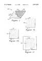
- FIG. 1is a partially cutaway, perspective view of the basic solid state image sensor, according to the present invention.
- FIG. 1Ais a plan view of the surface of a substrate having an array of photosensitive elements, according to the present invention.
- FIG. 1Bis a plan view of an alternate embodiment of the surface of a substrate having an array of photosensitive elements, according to the present invention.
- FIG. 1Cis a plan view of an yet another embodiment of the surface of a substrate having an array of photosensitive elements, according to the present invention.
- FIG. 2Ais a diagrammatic representation of a physical offset between lenslets and photosensitive elements, according to the present invention.
- FIG. 2Bis a diagrammatic representation of an alternate embodiment of a physical offset between lenslets and photosensitive elements, according to the present invention.
- FIG. 2Cis a diagrammatic representation of an embodiment of a virtual (rather than physical) between lenslets and photosensitive elements, according to the present invention.
- FIG. 3is a partially cut-away, perspective view of an alternate embodiment of the invention.
- FIG. 4is a partially cut-away, perspective view of yet another embodiment of the invention.
- FIG. 4Ais a side view of yet another embodiment of the invention.
- FIG. 4Bis a side view of yet another embodiment of the invention.
- FIG. 5is a perspective view of yet another embodiment of the invention.
- FIG. 6is a cross-sectional view of yet another embodiment of the invention.
- FIG. 7is a cross-sectional view of yet another embodiment of the invention.
- FIG. 8is a partially cut-away, perspective view of yet another embodiment of the invention.
- FIG. 9is a diagrammatic representation of yet another embodiment of the invention.
- FIG. 9Ais a diagrammatic representation of yet another embodiment of the invention.
- FIG. 9Bis a diagrammatic representation of yet another embodiment of the invention.
- FIG. 10is a diagrammatic representation of yet another embodiment of the invention.
- FIG. 11is a cross-sectional representation of yet another embodiment of the invention.
- FIG. 12is a cross-sectional representation of yet another embodiment of the invention.
- FIG. 13is a cross-sectional view of a television camera incorporating a solid-state image sensor according to the invention.
- FIG. 14Ais a block diagram of a security system incorporating a solid state image sensor according to the invention.
- FIG. 14Bis a block diagram of a video telephone system incorporating a solid state image sensor according. to the invention.
- FIG. 15is a partially diagrammatic, partially schematic view of a combined display and solid state image sensor arrangement.
- FIGS. 16A-Care cross-sectional views of various "sandwiched" display and solid-state image sensor arrangements, according to the invention.
- FIG. 16Dis a block diagram of a multiplexing system for simultaneous display and image capture, according to the invention.
- FIGS. 17A-Care views of various embodiments of combined display and image sensor arrangements affixed to a bracelet-type band, according to the invention.
- FIG. 18is a block diagram of a 2way audio/video communication device, according to the invention.
- FIG. 1show a solid state image sensor 100.
- a plurality of photosensitive elements 102(shown as dots "•") are formed on the front surface (up, in the figure) of a substrate 104.
- the photosensitive elements 102may be memory cells which discharge upon incidence of light, a CCD array, or any other suitable device which changes state or generates a potential or potential difference upon incidence of light.
- the substrate 104may be a silicon semiconductor die. Other suitable semiconducting materials may also be used.
- the photosensitive elements 102are arranged in an array of hundreds or thousands of rows and columns (only six rows and columns shown, for clarity). Preferably, the photosensitive elements are arranged in a square (m ⁇ m) or rectangular (m ⁇ n) array of evenly spaced elements.
- the photosensitive elements of one row (or column)can be offset from the elements of an adjacent row (or column).
- the photosensitive elements 102are arranged in a square array, and are arranged in columns and rows.
- the photosensitive elements 102'are arranged in a rectangular array on the surface of a substrate 104', and the photosensitive elements 102' of one row (or column) are offset from the photosensitive elements 102' of adjacent rows (or columns).
- an optically-transmissive layer 106is applied over the substrate, covering at least the entire array of elements 102 (or 102', or 102" discussed hereinbelow).
- the elements 102are shown covering substantially the entire surface of the substrate, it is within the scope of this invention that the array of elements occupies only a selected area, such as a central area 103 (dashed lines), of the substrate 104", as shown in FIG. 1C, where the photosensitive elements 102" cover only a central area 103 of the substrate 104".
- the photosensitive elements of one roware aligned with the photosensitive elements of an adjacent row, and the photosensitive elements of one column are aligned with the photosensitive elements of an adjacent column.
- the photosensitive elements of one roware offset from (located orthogonally between) the photosensitive elements of an adjacent row, and the photosensitive elements of one column are offset from the photosensitive elements of an adjacent column.
- the layer 106is formed of a suitably optically-transmissive material, such as silicon dioxide (SiO 2 ), spin-on glass, re-flow glass, photoresist, spin-on photoresist, re-flow photoresist, or the like, and is preferably of substantially uniform thickness.
- Spin-on and re-flow techniquesprovide relatively uniform thickness layers.
- the thickness of the layer 106is nonuniform, as initially applied, it is preferably planarized by chemical-mechanical polishing techniques, or the like.
- chemical-mechanical polishing techniquessee (e.g.) U.S. Pat. Nos. 4,671,851, 4,910,155 and 4,944,836, incorporated by reference herein.
- the layer 106can be applied as a sedimentary layer of relatively uniform thickness, as discussed in commonly-owned, copending U.S. patent application No. 906,902, entitled SEDIMENTARY DEPOSITION OF PHOTORESIST ON SEMICONDUCTOR WAFERS, filed Jun. 29, 1992 by Rostoker.
- the thickness of the layercan be verified by optical interference techniques, or the like, and adjusted to an appropriate final thickness.
- the layer 106is provided with a plurality of lens elements, or “lenslets” 108 (shown as circles “O").
- the lens elements 108are arranged in an array of hundreds or thousands of rows and columns (only six rows and columns shown, for clarity), corresponding on a one-to-one basis to the underlying elements 102.
- the lenslets (lens elements) 108are aligned over the photosensitive elements 102 in one of various ways discussed hereinbelow.
- the lens elements 108are formed as diffractive (binary) optical structures, but may be any lens or optical device which is capable of focusing an image onto the underlying photosensitive elements 102.
- each lenslet 108is generally directly over a corresponding photosensitive element 102, each pair of lenslets and corresponding photosensitive element is specifically arranged to sense a particular portion of an image being focused onto the substrate. This is accomplished in one of a variety of ways.
- FIG. 2Ashows an arrangement 200 of three lens elements 108a, 108b and 108c, over three corresponding photosensitive elements 102a, 102b and 102c.
- the photosensitive elementsare arranged in a regular array, with constant spacing "d" therebetween.
- the lens elementsare arranged in an irregular array, with varying spacing. More particularly, the lens element 108a is physically offset in one or two dimensions from the photosensitive element 102a. Thy lens element 108b is physically aligned with (directly over) the photosensitive element 102b.
- the lens element 108cis physically offset in an opposite (from the offset of 108a) direction from the photosensitive element 102c.
- each photosensitive element 102will provide information relating to one "pixel" of the image being focused onto the substrate.
- the plurality of photosensitive elementswill provide pixel information for the entire image of interest--each pixel representing a particular location on the image.
- the various physical offsets of the lens elementsare arranged to effect this result, namely by covering the entire two dimensional field of the image.
- FIG. 2Bshows an alternate arrangement 210 of three lens elements 108d, 108e and 108f, over three corresponding photosensitive elements 102d, 102e and 102f.
- the lens elementsare arranged in a regular (evenly spaced) array, with constant spacing "s" therebetween.
- the photosensitive elementsare arranged in an irregular (varying spacing) array. More particularly, the photosensitive element 102d is physically offset in one or two dimensions from the lens element 108d.
- the photosensitive element 102eis physically aligned with (directly under) the lens element 108e.
- the photosensitive element 102fis physically offset in an opposite (from the offset of 402e). direction from the lens element 108f.
- FIG. 2Cshows an alternate arrangement 220 of three lens elements 108g, 108h and 108i, over three corresponding photosensitive elements 102g, 102h and 102i.
- the lens elementsare arranged in a regular array, with constant spacing "s" therebetween, and the photosensitive elements are arranged in a regular array with constant spacing "d” therebetween.
- the lensletsare all physically aligned with the underlying photosensitive elements, with no physical offset.
- the lens elements 108g, 108h and 108iwere formed the same (same focusing parameters) as one another, this would result in all of the photosensitive elements 102g, 102h and 102i providing the same pixel information as the remaining photosensitive elements. Therefore, the lens elements 108g, 108h and 108i are each formed as binary (diffractive) optics, with unique focusing characteristics.
- the lenslet 108gis formed with its focal point offset in one or two dimensions from the photosensitive element 102g.
- the lenslet 108his formed with its focal point aligned with the photosensitive element 102h.
- the lenslet 108iis formed with its focal point offset in an opposite direction (vis-a-vis the lenslet 108g) from the photosensitive element 102e and is physically aligned with the lens element 102i. This provides a "virtual" offset for each pair of lenslets and photosensitive elements, in marked contrast to the "physical" offsets described with respect to FIGS. 2A and 2B.
- each photosensitive element 102will provide information relating to one "pixel" of the image being focused onto the substrate.
- the plurality of photosensitive elementswill provide pixel information for the entire image of interest--each pixel representing a particular location on the image.
- the various virtual offsetsare arranged to effect this result, namely by covering the entire two dimensions of the image.
- FIGS. 2A, 2B and 2CThe commonality between the arrangements of FIGS. 2A, 2B and 2C is that the relative orientation (whether physical or virtual or in combination) of the lenslets and photosensitive elements is arranged so that light from a selected portion of an image being focused by the lenslets onto the substrate is focused onto only one of the photosensitive elements, and in aggregate the photosensitive elements of the array provide a complete pixel-by-pixel image (i.e., signals representative of the incident image).
- light from a particular portion of an image being focused onto the die (substrate)is, however, focused by all of the lens elements 108 onto the substrate.
- the light from a particular portion of the imageis focused onto only one of the photosensitive elements 102.
- the light from that particular portion of the imageis focused onto the front surface of the substrate in areas between photosensitive elements 102.
- circuitrye.g., image processing circuitry
- Such circuitrymay be adversely affected by light.
- these areas between photosensitive elementsare preferably "masked" with an opaque layer, such as silicon nitride, aluminum or opaque photoresist (ink).
- FIG. 3shows an arrangement 300 similar to that of FIG. 1.
- a optically-opaque layer 310is applied over the substrate 304, and over any circuit elements (not shown) on the surface of the substrate.
- the layer 310is formed of any suitable material, such as silicon nitride, opaque photoresist, or the like, and is applied so as to have openings 312 (holes) in registration with the plurality of photosensitive elements 302 on the surface of the substrate.
- the array of photosensitive elementsmay cover only a portion of the surface of the substrate.
- An optically transmissive layer 306is applied over the masking layer 310, and can be applied to fill the holes while maintaining a relatively planar surface.
- the layer 306can also be chemical mechanically polished prior to forming lenslets in its exposed surface.
- Lenslets 308preferably diffractive
- lens elementse.g., 108, 308
- photosensitive elementse.g., 102, 302
- lens elementsit may be desirable to space the lens elements (e.g., 108, 308) further away from the photosensitive elements (e.g., 102, 302), while maintaining the integral structure of the substrate, photosensitive elements, masking layer (if used) and lens elements. This will allow greater flexibility in the design of the lenslets, such as increased depth of focus.
- FIG. 4shows an arrangement 400 similar to that of FIG. 1.
- an optically-transmissive layer 410is applied over the substrate 404, and over any circuit elements (not shown) on the surface of the substrate.
- the layer 410is preferably applied with uniform thickness, compensating for topological nonuniformities that may be caused by the underlying photosensitive elements (not shown) on the surface of the substrate.
- the layer 410is formed of any suitably optically-transmissive material, such as silicon dioxide (SiO 2 ), spin-on glass, re-flow glass, photoresist, spin-on photoresist, re-flow photoresist or the like, and is preferably of substantially uniform thickness. Spin-on and re-flow techniques provide relatively uniform thickness layers.
- the thickness of the layer 410is nonuniform, as initially applied, it is preferably planarized by chemical-mechanical polishing techniques, or the like.
- the layer 410can be applied as a sedimentary layer of relatively uniform thickness, as discussed hereinabove.
- the layer 310acted as a masking layer, to prevent light focused away from a photosensitive element from impacting on circuit elements between photosensitive elements, in this example, the layer 410 acts as a "standoff" to establish a suitable (increased) spacing for the overlying layer 406 containing lenslets 408.
- the array of photosensitive elements in the arrangement 400may cover only a portion of the surface of the substrate. Further, the techniques discussed with respect to FIGS. 1A, 1B, 2A, 2B and 2C are applicable with the spacing layer 410.
- FIG. 4Ashows an arrangement 420 wherein the teachings of FIGS. 3 and 4 are applied in combination.
- a masking layer 422(similar to 310) is applied over the substrate 404', with holes (not shown) aligned with the photosensitive elements (not shown).
- An optically-transmissive standoff layer 424(similar to 410) is applied over the masking layer 422.
- An optically-transmissive layer 406'is applied over the optically-transmissive standoff layer 424, and is provided with lenslets (not shown).
- FIG. 4Bshows an arrangement 440 wherein the teachings of FIGS. 3 and 4 are applied in combination.
- an optically-transmissive standoff layer 444(similar to 410) is applied over the substrate 404".
- An opaque masking layer 442(similar to 310) is applied over the standoff layer 444, and has holes aligned with the photosensitive elements (not shown).
- An optically-transmissive layer 406"is applied over the masking layer 442, and is provided with lenslets (not shown).
- the techniques discussed with respect to FIGS. 1A, 1B, 1C, 2A, 2B and 2Care applicable in this arrangement 420.
- lens elementse.g., 108, 308, 408
- photosensitive elementse.g., 102, 302, 402
- FIG. 5shows an arrangement 500 wherein a single, large lens element 508 is formed in an optically-transmissive layer 506 overlying an array of photosensitive elements 502 on a substrate 504.
- the lens element 508is formed as a single binary (diffractive) optical device, covering the. entire array of photosensitive elements 502.
- an optically-transmissive layer(not shown) is interposed between the single large lens element 508 and the surface of the substrate 504 (compare the optically-transmissive layer 410 of FIG. 4).
- FIG. 6shows an arrangement 600 where the lens element 608 is not integral with the substrate (as it was in the previous embodiments/arrangements). Rather, in this arrangement, a lens element 608 is mounted to vertical spacing members such as pins, posts, shims, or the side walls 622 of a package 620, or the like, containing the substrate 602 (array of photosensitive elements not shown).
- the side walls 622 of the package bodyestablish a known standoff for the lens element (i.e., distance between the lens element and the photosensitive array on the surface of the die). With the substrate 602, and the photosensitive array located in a predetermined location between the side walls 622, an accurate X-Y alignment of the lens 608 over the photosensitive array occurs.
- the lens element 608is preferably a refractive optic, similar to those described above (e.g., 108, 308, 408, 508), but in this case is nonintegral with the substrate. Further, the techniques discussed with respect to FIGS. 1A, 1B, 1C, 2A, 2B and 2C are applicable in this arrangement 600.
- the lens element 608can be formed as a conventional refractive lens which is also etched with a diffractive optical pattern.
- Such combination lens arrangementscould be used in any lens application (e.g., 108, 208, 308, 408, 508).
- FIG. 7shows an arrangement 700 similar to that of FIG. 6, in that a lens element 708 is supported above the substrate 702 by vertical pillars or posts/pins/shims, such as the side walls 722 of a package 720 (similar to 620), or the like. (The photosensitive array on the front surface of the die/substrate is not shown.) However, the substrate is also provided with an integral optic 788 on its front surface.
- the lens element 708can be a conventional refractive lens
- the substrate integral optic 788can be similar to any of the above-described diffractive elements (e.g., 108, 308, 408, 508)
- the lens element 708can be similar to any of the abovedescribed diffractive elements (e.g., 108, 308, 408, 508)
- the lens element 788can be a conventional refracting lens mounted to the surface of the substrate.
- either lens element 708 or 788may be a combination lens of conventional cum binary or conventional cum refractive lenses.
- the "mixed" optics 708 and 788can be designed to eliminate spherical and/or chromatic aberration. Filters may also be used to remove light having a wavelength subject to chromatic aberration and not otherwise corrected for by the use of "mixed optics".
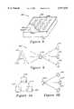
- FIG. 8shows an arrangement 800 suited for color imaging.
- An array of photosensitive elements 802are arranged on the front surface of a substrate 804, in a manner similar to the photosensitive elements 102 (e.g.). However, in this arrangement 800, at each array location, there are three closely grouped together photosensitive elements ("triplets”) 802a, 802b, 802c, rather than a single photosensitive element 102. A 4 ⁇ 4 array is shown, for illustrative clarity.
- An optically-transmissive layer 806(similar to 106) is formed over the array of photosensitive element triplets. In this case, there is one lenslet 808 for each "triplet" of photosensitive elements.
- the lens elementsare preferably formed as diffractive elements (or a combination lens), and are designed to have different focal points for different wavelengths of light. For example, red (R) light can be focused onto the element 802a of a triplet, green (G) light can be focused onto the element 802b of the triplet, and blue (B) light can be focused onto the element 802c of the triplet. In this manner, color imaging can be achieved.
- red (R) lightcan be focused onto the element 802a of a triplet
- green (G) lightcan be focused onto the element 802b of the triplet
- blue (B) lightcan be focused onto the element 802c of the triplet.
- color imagingcan be achieved.
- FIG. 9shows an alternate arrangement 900 of a color capable solid state image sensor.
- the arrangement of FIG. 8 aemployed a single substrate (die), and triplets of photosensitive elements
- this arrangement 900three solid-state image sensors 902, 904, 906 are employed, each of which is suited to monochromatic image sensing.
- Each image sensor 902, 904, 906is formed in a manner similar to the sensor 100 of FIG. 1 (and the enhancements to the FIG. 1 embodiment, discussed hereinabove, are equally applicable).
- An image 910 (“A")is focused by any suitable optics (not shown) through a beam splitter 912.
- the beam splitter 912is preferably a diffractive optic that is designed to direct different wavelengths of light at different angles.
- the beam splitter 912directs red (R) light towards the sensor 902, directs green (G) light towards the sensor 904, and directs blue (B) light towards the sensor 906.
- the beam splitter 912can be designed to accommodate a linear, planar arrangement of sensors 902, 904, 906, as shown.
- the three sensors 902', 904' and 906'can be arranged in a planar, triangular (e.g., equilateral) pattern, as shown in FIG. 9A, so that the angles to each of the sensors from the beam splitter 912' are preferably, but not necessarily equal but differently oriented.
- the three sensors 902", 904", 906"can be arranged in a curved, linear array, as shown in FIG.
- the distancecan correspond to the focal length (in the usual sense of the term) of the lens.
- the distancecan be sufficient to permit a predetermined mapping of the image onto the sensors.
- the mappingmay be either a one tone mapping or may instead be sufficient to be used in combination with a compression or decompression algorithm.
- focal lengthas defined herein for each of the embodiments of the present invention should be construed to include both of these definitions, and specifically to include the distance necessary to produce a focal plane image with one tone correspondence with a "viewed" object, in addition to the usual meaning of the term "focal length.”
- the three sensors of any of these embodimentscan be arranged on any suitable mounting substrate.
- the three sensors of FIGS. 9A and 9Bcan be disposed in a package similar to that of FIGS. 6 or 7.
- the optical element 708 of FIG. 7could function as a beam splitter (912), and three sensors, each having its own integral focusing optic could be disposed within the cavity of the package (each in a manner similar to 702/788).
- FIG. 10shows a chip 1000 including an image sensing array 1001.
- the chipalso includes a logic array 1002 for processing the signals generated by the array 1001.
- the chipmay also include a memory array 1003 for storing signals generated by array 1001 or array 1002.
- the logic array 1002 and/or memory array 1003can be an embedded array as described in, e.g., U.S. patent application Ser. No. 07/596,680.
- the memory array 1003can be a "cache memory.”
- FIG. 11shows a cross-sectional view of a method of forming a chip in accordance with an embodiment of the present invention.
- a substrate 1104is coated successively with a first optically transmissive layer 1103, such as spun on glass, a second optically transmissive layer 1102, such as pyrolitic silicon dioxide, and a layer of photoresist 1101.
- the photoresist 1101is exposed and developed by conventional techniques.
- the photoresist 1101is then used as a mask to etch second optically transmissive layer 1102. Any suitable etching technique can be used.
- reactive ion etchingis used when vertical sidewalls are desired.
- wet chemical etchingmay also be used, alone or in combination with reactive ion etching, to create more rounded geometries where appropriate.
- a laser beamis used to improve the shape of the lens, and to correct any defects in the lens shape which may be detected during testing. If desired, the entire lens may beshaped by the use of the laser. This avoids the need for masking and etching, but reduces throughput.
- Diffractive lenses for use in accordance with the present inventionmay be produced by any suitable technique.
- such lensesare shaped by chem-mech polishing or etching.
- layer 1202represents the second optically transmissive layer after the coating and etching step.
- layer 1202has been formed into a fresnel or binary lens structure.
- the first optically transmissive layer 1203provides a gap between the substrate 1204 which permits the lens 1202 to focus an image on an appropriate area of the substrate 1204 having one or more image sensing devices.
- FIG. 13is a cross-sectional view of a television camera 1300, incorporating a solid state image sensor 1310 of the type described hereinabove.
- a solid state image sensor 1310of the type described hereinabove.
- Any of the solid-state image sensors described hereinaboveare suitable in this arrangement, for example, 300 as described hereinabove with respect to FIG. 3.
- the image sensor 1310is mounted within a housing 1320, and provides a video output signal 1312.
- a variable focus optical system 1330is mounted to the housing 1320 over the solid-state image sensor 1310. Because of the small size of the solid-state image sensor, it is possible to provide an extremely small camera capable of application in very tight spaces or in applications, such as security systems, where it may be desirable that the camera be hidden.
- variable focus optical system 1330is shown having one or more lenses, such as lenses 1340 and 1350, which may be conventional, binary, or other refractive or diffractive or combination lenses, with a sliding system 1360, well known in the camera technology, to vary the focal length. Other means for varying the focal length are contemplated.
- variable focus optical system 1330is not essential to the operation of the television camera 1300, since the solid-state image sensors described herein have builtin optical systems providing fixed focus. However, the variable focus optical system 1330 permits alteration of the basic focal length of the solid-state image sensor 1310 and provides a wider range of distances over which the camera 1300 will operate effectively.
- Such a camera 1300may also be equipped with an aperture control 1380 (such as an iris) to control the intensity of light transmitted to the image sensor.
- an aperture control 1380such as an iris
- circuitrycould be utilized with the image sensor to enhance or subdue sensitivity to variable ambient light characteristics about the camera/sensor.
- variable focus optical system 1330could be substituted for the variable focus optical system 1330 to provide a different focal length than that provided by the solid-state image sensor for such specialized applications as dedicated inspection systems, microscope cameras, telescope cameras, etc.
- FIG. 14Ais a block diagram of a basic security system comprising a television camera 1410a of the type (1300) described with respect to FIG. 13 and television monitor 1430a.
- a video signal 1420 representing an image "seen" by the camera 1410ais connected to the monitor causing a representation of the image to be displayed on the monitor 1430a.
- An intermediate memory or processormay be utilized to store or modify the signal 1420 prior to display.
- the extremely small camera size afforded by the application of a solid-state image sensorpermits applications involving location and positioning of the camera 1410 in places which might otherwise be difficult or impossible.
- FIG. 14Bis a block diagram of a video telephone system 1400b comprising a camera 1410b of the type (e.g., 1300) described hereinabove with respect to FIG. 13, a transmitting line interface 1440b, a receiving line interface 1440b, and a television monitor 1430b.
- a video signal 1420b from the camera 1410bis interfaced to and transmitted over a communication line 1450b by the transmitting line interface 1440b.
- the communication line 1450bmay be, for example, a dialed telephone connection across a commercial switched telephone network.
- the receiving line interface 1440bconverts the signal received over the communication line back into a video signal and transmits it through line 1460b (for possible storage by memory and/or signal processing--not shown) before or after is may be displayed on the monitor 1430b.
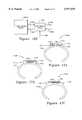
- FIGS. 15, 16A-D, and 17A-Care directed to combined arrangements of solid-state image sensors and LCD display panels. These combined arrangements are effectively image sensing display panels capable of both image display and image capture. LCD panels, for display purposes, are well known.
- FIG. 15is a view of a combined display and image sensor 1500.
- a solid state image sensor 1510(“camera") providing a "Camera” output signal 1515 (video signal) and an LCD (Liquid Crystal Display) Panel (Display) 1520 are mounted side by side on a common substrate (backing) 1530.
- the LCDmay alternatively be a plasma screen display or other. suitable display means for the purpose, all included in the term “LCD” or "Liquid Crystal Display”.
- An electrical interface 1525 to the LCD panel 1520provides data to be displayed on the LCD panel.
- the "camera” output signal 1515is. an electrical analog of the image "seen” by the solid-state image sensor 1510.
- FIG. 16Ais a view of a sandwiched display/image sensor arrangement.
- a binary optic element 1610e.g., lens element 788, FIG. 7
- a combination lens elementis disposed over a an array of photosensitive elements 1620 (e.g., 702, FIG. 7 or 802, FIG. 8). These two elements are disposed over an LCD display panel 1630.
- the binary optic element 1610 and array of photosensitive elements 1620in combination, form an image sensor.
- the image sensorvia the array of photosensitive elements 1620, produces a video output signal 1640, representative of an image "seen" by the array 1620.
- the LCD display panel 1630is responsive to signals on an LCD electrical interface 1650 to produce a visible image.
- the binary optic element 1610 and array of photo-sensitive elements 1620are sufficiently transmissive of light that an image displayed on the LCD display panel 1630 may be seen through them by an observer.
- the visibility of the image on the LCD display panelmay be augmented through the use of back-lighting means 1660 (light shown as arrows ()) such as an electro-luminescent panel (“EL" panel) or fluorescent lighting tubes.
- back-lighting means 1660such as an electro-luminescent panel (“EL" panel) or fluorescent lighting tubes.
- FIG. 16Bis a view of another embodiment 1600b of a sandwiched display/image sensor arrangement, similar to that described with respect to FIG. 16A. All of the same elements (binary or combination optic element 1610, photo-sensitive array 1620, and LCD display panel 1630) are employed in this display/image sensor arrangement 1600b, but are arranged in a different order.
- the LCD display panel 1630overlies the binary optic element 1610, which in turn overlies the photosensitive array 1620.
- an LCD panele.g. 1630
- the display panel 1630By causing the display panel 1630 to be transmissive of light (transparent) by applying appropriate electrical signals via the electrical interface 1650, sufficient light reaches the photosensitive array to cause an image to be formed thereupon. This image is then converted by the photosensitive array 1620 into an electrical video signal 1640 which is representative of the image. It is also possible, by making the LCD panel 1630 opaque, to block light to the photosensitive array 1620, thereby blocking any image which would otherwise be formed thereupon. Additionally, through memory or processing means (not shown) described previously, the LCD panel 1630 may display a separate image than what is being viewed by the photosensitive array 1620.
- signals provided to the LCD panel 1630 over the LCD electrical interface 1650permit an image to be formed on the LCD panel in the form of opaque and transmissive areas on the LCD panel.
- the viewability of this imagemay be augmented by back-lighting means 1660.
- Such systemsshown in FIGS. 16A-C, could also display in color with color LCD panels or the like in combination with, for example, a color photo-sensitive array system (e.g., 800, FIG. 8).
- FIG. 16Cis a view of another embodiment 1600c of a sandwiched display/image sensor arrangement, including means 1660 for backlighting.
- the binary optic element 1610overlies the LCD panel 1630, which in turn overlies the photosensitive array 1620.
- the binary optic or combination element 1610is sufficiently transmissive of light that an image formed on the LCD panel 1630 may be viewed through the binary optic element 1610.
- the LCD panel 1630can be made sufficiently transmissive of light (by application of appropriate signals to the LCD electrical interface 1650) to permit an image to be formed through the binary optic element 1610 and LCD panel 1630 onto the photosensitive array 1620.
- the backlighting means 1660enhances the viewability of any image on the LCD panel 1630.
- the sandwiched display/image sensor arrangements 1600a-1600c described hereinaboveit is possible, by multiplexing the operation of the LCD display panel 1630 and the photo-sensitive array 1620, to simultaneously display a viewable image on the LCD display panel 1630 and to capture and transmit an image formed on the photosensitive array 1620. This is accomplished by rapidly alternating the LCD display panel 1630 between displayed image and a transparent (transmissive) state via the LCD electrical interface 1650.
- the video signal 1640is monitored only when the LCD display panel 1630 is in its transparent state.
- the alternation of the LCD display panel 1630occurs at a rate sufficiently high that a human observer does not notice any significant "flicker" of the image.
- the displaymay be monitored when the display is in either state.
- any of the three embodimentsmay employ backlighting (e.g., 1660, FIG. 16C), but backlighting will generally interfere with the operation of the photosensitive array 1620. As a result, it is necessary to "turn off" the backlighting means 1660 while the video signal 1640 from the photosensitive array 1620 is being monitored.
- the embodiment of FIG. 16A (1600a)provides a convenient method for accomplishing this. Since the LCD display panel 1630 is behind the photosensitive array 1620, placing the LCD display panel 1630 into a completely opaque state would cause any light from backlighting means (e.g., 1660) placed behind the LCD display panel 1630 to be blocked. In this way, the LCD display panel 1630 acts as a sort of "shutter” between a back-lighting means and the photosensitive array 1620.
- the backlighting meanswould remain "on", and the LCD display panel 1630 would be caused to alternate between a displayed image and an opaque state.
- the video signal 1640 from the photosensitive arraywould then be monitored only when the LCD display panel 1630 is in the opaque state.
- the LCD display panel 1630can be selectively darkened (by pattern or "gray-scale") to limit the light that would impinge on the photo-sensitive array 1620 as another "shutter” means or light intensity control means where the panel 1630 is in front of the array 1620 (e.g., FIG. 16B and 16C).
- an LCD display panel 1630which, in its opaque state, blocks light frequencies which are visible to the human eye, but passes some light frequencies (e.g., infra-red) which are outside of the range of frequencies visible to humans.
- Optical an optical filtermay be employed to limit the light frequency. response of the photosensitive array 1620.
- the photosensitive array 1620is insensitive to the light frequency or frequencies produced by the back-lighting means 1660, then it not necessary to modulate (switch on and off) the backlighting means 1660 while the photo-sensitive array is capturing an image.
- FIG. 16Dis a block diagram of an arrangement for accomplishing this alternating, multiplexed operation of a sandwiched display/image sensor arrangement 1600d. Any of the three aforementioned sandwiched display image sensor arrangements 1600a-1600c may be used.
- a multiplexing circuit 1670receives image data 1655 to be displayed on the LCD display panel 1630, and causes the LCD display panel 1630 to alternate between displaying the image and assuming either a transparent state (as described above with respect to 1600b or 1600c) or an opaque state (as describe above with respect to 1600a).
- the multiplexing operationis controlled by a synchronizing multiplex control signal 1690, which governs the rate and duty cycle at which the transparent (or opaque) state is assumed by the LCD display panel 1630.
- This same multiplex control signal 1690is used to control when the video signal 1640 from the photosensitive array 1620 is monitored, so that the video signal 1640 is only “filtered” by the multiplexing circuit 1670.
- the "filtered” video signalis output by the multiplexing circuit 1670 as image sensor data 1645.
- a large glass, ceramic or plasticmay be used for the substrate of the photosensitive array, and the photosensitive elements may be disposed thereupon. This permits image sensor arrays of arbitrary size to be fabricated. Additionally, with all photo-sensitive elements as well as logic and memory circuit elements disposed on the display substrate, an efficient lightweight and easily manufactured system may be developed.
- the substratemay be formed by depositing amorphous or poly-silicon on a continuous sheet of metal, such as aluminum. Techniques similar to this are currently employed in the production of photo-voltaic cells.
- One embodiment of this typeinvolves sizing and shaping such a large sandwiched display/image sensor arrangement to approximately match the size and shape of a "sheet” (of, e.g., 8.5 inch by 11 inch paper).
- the effective focal length and aim of the lD integral optically transmissive elemente.g., binary optics
- a sheet of papercould be held (or laid) directly on the image sensing panel. This would provide a page sized reader (such as optical character recognition (OCR) readers or graphics readers) in the same device as the display for computer systems and the like.
- OCRoptical character recognition
- FIGS. 17A-Care views of various embodiments of a bracelet-mounted display/image sensor arrangement.
- FIG. 17Ais a view of an arrangement 1700a whereby a solid-state image sensor 1720 and an LCD display panel 1730 are mounted to a mounting surface 1725 attached to a bracelet-type band 1710, sized and shaped to fit around a human wrist.
- a clothespin or clip devicemay be used to hold the display/camera devices (1720, 1730).
- a housing 1740 with an optically transmissive element 1750covers the LCD display panel 1730 and the solid-state image sensor 1720.
- the optically transmissive elementmay be a nonrefractive element (e.g., a sheet of glass, quartz crystal, or transparent acrylic) or a refractive or diffractive or combination element (lens).
- Electronic control circuitry(not shown), which is powered (not shown) as by a battery, controls the operation of the LCD display panel 1730 and solid-state image sensor 1720.
- FIG. 17Bis a view of another similar arrangement 1700b, this time employing a sandwiched display/image sensor arrangement 1735.
- Electronic circuitry(not shown), such as that described hereinabove, controls the operation of the display/image sensor arrangement 1735.
- the arrangement 1735may be of the forms shown in FIGS. 16A-C as 1600a, 1600b, or 1600c and may be backlighted.
- FIG. 17Cis a view of another similar embodiment 1700c, wherein a bracelet-type band 1710a has an integrally formed housing and mounting surface 1745.
- the optically transmissive element 1750mounts directly to the bracelet-type band over the sandwiched display/image sensor arrangement 1735.
- electronic circuitry(not shown), controls the operation of the display/image sensor arrangement 1735.
- no upper element (or lens) 1750may be needed.
- the wrist band type sensor of FIGS. 17A-Cwould be suitable, with attendant communication circuitry, a microphone, audiocapture circuitry, audio reproduction circuitry and a speaker to be useful as a "Dick Tracy" type watch, enabling voice and picture communication, e.g., through a cellular phone system or other wireless communication means.
- voice and picture communicatione.g., through a cellular phone system or other wireless communication means.
- suchwould be an excellent input and output device for, e.g., a computer or security system and could be connected to such system.
- FIG. 18is a block diagram of such a two-way voice and picture (audio/video) communication system.
- a first audio/video communication device 1800aof the type mentioned above (e.g., "Dick Tracy" watch) transmits and receives communication signals 1820 over a wireless communication medium via a wireless communication circuit 1820, (e.g., a cellular telephone circuit).
- a camera chip 1802 of the type described hereinabove and an LCD display panel 1804,provide means 1801 for image capture and display.
- An image sensing display panel of the type described hereinabovee.g., 1600a, 1600b, or 1600c, FIGS. 16A-C
- Camera and LCD control circuitry 1806provides means for processing electrical signals 1805 from the camera 1802 and provides electrical signals 1803 to the LCD display 1804.
- An audio circuit 1814connects to the wireless communication circuit 1808, exchanging audio signals 1815 with the wireless communication circuit 1808.
- the audio circuit 1814receives an electrical signal 1811 from a microphone 1810 converting it into a form suitable for transmission by the wireless communication circuit 1808.
- the signals received (audio signals) from the wireless communication circuit 1808 by the audio circuit 1814are converted by the audio circuit 1814 into speaker electrical signals 1813 to be reproduced a speaker 1813. It is known in the art to use a single transducer as both a speaker and a microphone. If this approach is used, a separate microphone (e.g., 1810) and speaker (e.g., 1812) are not required.
- the first two-way audio/video communication device 1800acommunicates via the communication signals with a second two-way audio/video communication device 1800b.
- the second communication device 1800bmay be identical to the first communication device 1800a, or may be an equivalent device or devices, such as a conventional videophone.
Landscapes
- Engineering & Computer Science (AREA)
- Multimedia (AREA)
- Signal Processing (AREA)
- Solid State Image Pick-Up Elements (AREA)
- Transforming Light Signals Into Electric Signals (AREA)
Abstract
Description
Claims (21)
Priority Applications (1)
| Application Number | Priority Date | Filing Date | Title |
|---|---|---|---|
| US08/863,372US5977535A (en) | 1992-09-30 | 1997-05-27 | Light sensing device having an array of photosensitive elements coincident with an array of lens formed on an optically transmissive material |
Applications Claiming Priority (5)
| Application Number | Priority Date | Filing Date | Title |
|---|---|---|---|
| US95495892A | 1992-09-30 | 1992-09-30 | |
| US1720293A | 1993-02-11 | 1993-02-11 | |
| US08/287,204US5519205A (en) | 1992-09-30 | 1994-08-08 | Color electronic camera including photosensor array having binary diffractive lens elements |
| US57874696A | 1996-12-26 | 1996-12-26 | |
| US08/863,372US5977535A (en) | 1992-09-30 | 1997-05-27 | Light sensing device having an array of photosensitive elements coincident with an array of lens formed on an optically transmissive material |
Related Parent Applications (1)
| Application Number | Title | Priority Date | Filing Date |
|---|---|---|---|
| US57874696AContinuation | 1992-09-30 | 1996-12-26 |
Publications (1)
| Publication Number | Publication Date |
|---|---|
| US5977535Atrue US5977535A (en) | 1999-11-02 |
Family
ID=26689586
Family Applications (4)
| Application Number | Title | Priority Date | Filing Date |
|---|---|---|---|
| US08/287,128Expired - LifetimeUS5760834A (en) | 1992-09-30 | 1994-08-08 | Electronic camera with binary lens element array |
| US08/287,204Expired - LifetimeUS5519205A (en) | 1992-09-30 | 1994-08-08 | Color electronic camera including photosensor array having binary diffractive lens elements |
| US08/578,746Expired - LifetimeUS5648655A (en) | 1992-09-30 | 1995-12-26 | Sensing device for capturing a light image |
| US08/863,372Expired - LifetimeUS5977535A (en) | 1992-09-30 | 1997-05-27 | Light sensing device having an array of photosensitive elements coincident with an array of lens formed on an optically transmissive material |
Family Applications Before (3)
| Application Number | Title | Priority Date | Filing Date |
|---|---|---|---|
| US08/287,128Expired - LifetimeUS5760834A (en) | 1992-09-30 | 1994-08-08 | Electronic camera with binary lens element array |
| US08/287,204Expired - LifetimeUS5519205A (en) | 1992-09-30 | 1994-08-08 | Color electronic camera including photosensor array having binary diffractive lens elements |
| US08/578,746Expired - LifetimeUS5648655A (en) | 1992-09-30 | 1995-12-26 | Sensing device for capturing a light image |
Country Status (1)
| Country | Link |
|---|---|
| US (4) | US5760834A (en) |
Cited By (71)
| Publication number | Priority date | Publication date | Assignee | Title |
|---|---|---|---|---|
| US20020122124A1 (en)* | 2000-10-25 | 2002-09-05 | Yasuo Suda | Image sensing apparatus and its control method, control program, and storage medium |
| US20030193599A1 (en)* | 2002-03-27 | 2003-10-16 | Marconi Communications, Inc. | Method and apparatus for displaying images in combination with taking images |
| US6683645B1 (en)* | 1995-12-01 | 2004-01-27 | Qinetiq Limited | Imaging system with low sensitivity to variation in scene illumination |
| US20040037457A1 (en)* | 2002-08-26 | 2004-02-26 | Eastman Kodak Company | Detecting and classifying blemishes on the transmissive surface of an image sensor package |
| US20040105026A1 (en)* | 1998-12-24 | 2004-06-03 | Campbell Scott Patrick | Contoured surface cover plate for image sensor array |
| US6809774B1 (en)* | 1998-11-06 | 2004-10-26 | Fuji Photo Film Co., Ltd. | Wrist-carried camera and watch-type information equipment |
| US6867821B2 (en)* | 2000-07-31 | 2005-03-15 | Koninklijke Philips Electronics N.V. | Image-sensing display device with particular lens and sensor arrangement |
| US20050110889A1 (en)* | 2003-11-26 | 2005-05-26 | Tuttle Mark E. | Packaged microelectronic imagers and methods of packaging microelectronic imagers |
| US20050184219A1 (en)* | 2004-02-23 | 2005-08-25 | Kirby Kyle K. | Packaged microelectronic imagers and methods of packaging microelectronic imagers |
| US20050226319A1 (en)* | 2004-03-19 | 2005-10-13 | Sony Corporation | Information processing apparatus and method, recording medium, program, and display device |
| US20050255628A1 (en)* | 2003-09-18 | 2005-11-17 | Micron Technology, Inc. | Microelectronic devices and methods for packaging microelectronic devices |
| US20050254133A1 (en)* | 2004-05-13 | 2005-11-17 | Salman Akram | Integrated optics units and methods of manufacturing integrated optics units for use with microelectronic imagers |
| US20050270651A1 (en)* | 2004-06-02 | 2005-12-08 | Boettiger Ulrich C | Apparatus and method for manufacturing positive or negative microlenses |
| US20050275750A1 (en)* | 2004-06-09 | 2005-12-15 | Salman Akram | Wafer-level packaged microelectronic imagers and processes for wafer-level packaging |
| US20050275048A1 (en)* | 2004-06-14 | 2005-12-15 | Farnworth Warren M | Microelectronic imagers and methods of packaging microelectronic imagers |
| US20050275049A1 (en)* | 2004-06-10 | 2005-12-15 | Kirby Kyle K | Packaged microelectronic imagers and methods of packging microelectronic imagers |
| US20050275051A1 (en)* | 2004-06-14 | 2005-12-15 | Farnworth Warren M | Prefabricated housings for microelectronic imagers and methods for packaging microelectronic imagers |
| US20050285154A1 (en)* | 2004-06-29 | 2005-12-29 | Salman Akram | Packaged microelectronic imagers and methods of packaging microelectronic imagers |
| US20060011809A1 (en)* | 2004-07-19 | 2006-01-19 | Farnworth Warren M | Microelectronic imagers with optical devices and methods of manufacturing such microelectronic imagers |
| US20060014313A1 (en)* | 2004-07-16 | 2006-01-19 | Hall Frank L | Microelectronic imaging units and methods of manufacturing microelectronic imaging units |
| US20060024856A1 (en)* | 2004-07-28 | 2006-02-02 | Derderian James M | Microelectronic imaging units and methods of manufacturing microelectronic imaging units |
| US20060038183A1 (en)* | 2004-08-19 | 2006-02-23 | Oliver Steven D | Microelectronic imagers with curved image sensors and methods for manufacturing microelectronic imagers |
| US20060040421A1 (en)* | 2004-08-19 | 2006-02-23 | Farnworth Warren M | Spacers for packaged microelectronic imagers and methods of making and using spacers for wafer-level packaging of imagers |
| US20060043599A1 (en)* | 2004-09-02 | 2006-03-02 | Salman Akram | Through-wafer interconnects for photoimager and memory wafers |
| US20060044433A1 (en)* | 2004-08-31 | 2006-03-02 | Micron Technology, Inc. | Microelectronic imagers having front side contacts and methods of packaging such microelectronic imagers |
| US20060043262A1 (en)* | 2004-08-30 | 2006-03-02 | Micron Technology, Inc. | Microelectronic imagers with integrated optical devices and methods for manufacturing such microelectronic imagers |
| US20060043509A1 (en)* | 2004-08-24 | 2006-03-02 | Watkins Charles M | Packaged microelectronic imaging devices and methods of packaging microelectronic imaging devices |
| US20060043512A1 (en)* | 2004-08-24 | 2006-03-02 | Oliver Steven D | Microelectronic imagers with optical devices having integral reference features and methods for manufacturing such microelectronic imagers |
| US20060046332A1 (en)* | 2004-08-26 | 2006-03-02 | Derderian James M | Microelectronic Imaging units and methods of manufacturing microelectronic imaging units |
| US20060098097A1 (en)* | 2004-09-13 | 2006-05-11 | Wach Hans B | Iris image capture devices and associated systems |
| US20060148250A1 (en)* | 2004-12-30 | 2006-07-06 | Micron Technology, Inc. | Methods for forming interconnects in microelectronic workpieces and microelectronic workpieces formed using such methods |
| US20060177999A1 (en)* | 2005-02-10 | 2006-08-10 | Micron Technology, Inc. | Microelectronic workpieces and methods for forming interconnects in microelectronic workpieces |
| US20060177959A1 (en)* | 2005-02-10 | 2006-08-10 | Micron Technology, Inc. | Microfeature workpieces having microlenses and methods of forming microlenses on microfeature workpieces |
| US20060175532A1 (en)* | 2005-02-08 | 2006-08-10 | Micron Technology, Inc. | Microelectronic imaging units and methods of manufacturing microelectronic imaging units |
| US20060186492A1 (en)* | 2005-02-18 | 2006-08-24 | Micron Technology, Inc. | Microelectronic imagers with shaped image sensors and methods for manufacturing microelectronic imagers |
| US20060216850A1 (en)* | 2004-08-10 | 2006-09-28 | Street Bret K | Microelectronic imaging units and methods of manufacturing microelectronic imaging units |
| US20060289968A1 (en)* | 2005-06-28 | 2006-12-28 | Micron Technology, Inc. | Conductive interconnect structures and formation methods using supercritical fluids |
| GB2429596A (en)* | 2005-08-26 | 2007-02-28 | Avago Tech Ecbu Ip | Determining camera shake using multiple motion sensors |
| US20070045858A1 (en)* | 2005-09-01 | 2007-03-01 | Micron Technology, Inc. | Microfeature workpieces and methods for forming interconnects in microfeature workpieces |
| US20070045515A1 (en)* | 2005-09-01 | 2007-03-01 | Micron Technology, Inc. | Microelectronic imaging devices and associated methods for attaching transmissive elements |
| US7232754B2 (en) | 2004-06-29 | 2007-06-19 | Micron Technology, Inc. | Microelectronic devices and methods for forming interconnects in microelectronic devices |
| US20070148807A1 (en)* | 2005-08-22 | 2007-06-28 | Salman Akram | Microelectronic imagers with integrated optical devices and methods for manufacturing such microelectronic imagers |
| US20080062300A1 (en)* | 2006-09-08 | 2008-03-13 | Hon Hai Precision Industry Co., Ltd. | Electronic device and image-sensing device thereof |
| US7425499B2 (en) | 2004-08-24 | 2008-09-16 | Micron Technology, Inc. | Methods for forming interconnects in vias and microelectronic workpieces including such interconnects |
| US7448910B2 (en) | 2004-09-03 | 2008-11-11 | Samsung Electronics Co., Ltd | Displaying apparatus |
| US7622377B2 (en) | 2005-09-01 | 2009-11-24 | Micron Technology, Inc. | Microfeature workpiece substrates having through-substrate vias, and associated methods of formation |
| EP1728382A4 (en)* | 2004-03-17 | 2010-07-28 | Thomas Jeff Adamo | Apparatus for imaging using an array of lenses |
| US20100194465A1 (en)* | 2009-02-02 | 2010-08-05 | Ali Salih | Temperature compensated current source and method therefor |
| US20100272327A1 (en)* | 2003-12-01 | 2010-10-28 | Silveira Paulo E X | Task-Based Imaging Systems |
| US20110019055A1 (en)* | 2009-07-24 | 2011-01-27 | Jaworski Frank B | Integrate detect and display |
| US20110026141A1 (en)* | 2009-07-29 | 2011-02-03 | Geoffrey Louis Barrows | Low Profile Camera and Vision Sensor |
| US8013895B2 (en) | 2006-08-07 | 2011-09-06 | Avago Technologies General Ip (Singapore) Pte. Ltd. | Optical motion sensing |
| US8092734B2 (en) | 2004-05-13 | 2012-01-10 | Aptina Imaging Corporation | Covers for microelectronic imagers and methods for wafer-level packaging of microelectronics imagers |
| US8318579B1 (en) | 2011-12-01 | 2012-11-27 | United Microelectronics Corp. | Method for fabricating semiconductor device |
| US20130122247A1 (en)* | 2011-11-10 | 2013-05-16 | Omnivision Technologies, Inc. | Spacer Wafer For Wafer-Level Camera And Method For Manufacturing Same |
| US8466000B2 (en) | 2011-04-14 | 2013-06-18 | United Microelectronics Corp. | Backside-illuminated image sensor and fabricating method thereof |
| US8779344B2 (en) | 2012-07-11 | 2014-07-15 | United Microelectronics Corp. | Image sensor including a deep trench isolation (DTI)that does not contact a connecting element physically |
| US8779484B2 (en) | 2012-11-29 | 2014-07-15 | United Microelectronics Corp. | Image sensor and process thereof |
| US8815102B2 (en) | 2012-03-23 | 2014-08-26 | United Microelectronics Corporation | Method for fabricating patterned dichroic film |
| US8828779B2 (en) | 2012-11-01 | 2014-09-09 | United Microelectronics Corp. | Backside illumination (BSI) CMOS image sensor process |
| US9054106B2 (en) | 2013-11-13 | 2015-06-09 | United Microelectronics Corp. | Semiconductor structure and method for manufacturing the same |
| US9070612B2 (en) | 2011-07-05 | 2015-06-30 | United Microelectronics Corporation | Method for fabricating optical micro structure and applications thereof |
| US9129876B2 (en) | 2013-05-28 | 2015-09-08 | United Microelectronics Corp. | Image sensor and process thereof |
| US9279923B2 (en) | 2013-03-26 | 2016-03-08 | United Microelectronics Corporation | Color filter layer and method of fabricating the same |
| US9312292B2 (en) | 2011-10-26 | 2016-04-12 | United Microelectronics Corp. | Back side illumination image sensor and manufacturing method thereof |
| US9401441B2 (en) | 2012-06-14 | 2016-07-26 | United Microelectronics Corporation | Back-illuminated image sensor with dishing depression surface |
| US9537040B2 (en) | 2013-05-09 | 2017-01-03 | United Microelectronics Corp. | Complementary metal-oxide-semiconductor image sensor and manufacturing method thereof |
| US9841319B2 (en) | 2013-11-19 | 2017-12-12 | United Microelectronics Corp. | Light detecting device |
| US10136204B1 (en)* | 2014-09-30 | 2018-11-20 | Amazon Technologies, Inc. | Audio assemblies for electronic devices |
| US10677964B2 (en) | 2017-10-23 | 2020-06-09 | Omnivision Technologies, Inc. | Lens wafer assembly and associated method for manufacturing a stepped spacer wafer |
| WO2020149115A1 (en)* | 2019-01-16 | 2020-07-23 | ソニーセミコンダクタソリューションズ株式会社 | Display element and projection display device |
Families Citing this family (47)
| Publication number | Priority date | Publication date | Assignee | Title |
|---|---|---|---|---|
| US5529936A (en)* | 1992-09-30 | 1996-06-25 | Lsi Logic Corporation | Method of etching a lens for a semiconductor solid state image sensor |
| US5760834A (en)* | 1992-09-30 | 1998-06-02 | Lsi Logic | Electronic camera with binary lens element array |
| GB2282906B (en) | 1993-10-13 | 1996-11-06 | Dataquill Ltd | Data enty systems |
| JPH08233658A (en)* | 1995-02-24 | 1996-09-13 | Olympus Optical Co Ltd | Spectroscope and spectral image recorder |
| CA2222741C (en) | 1995-06-06 | 2002-05-28 | Vincent Chow | Multi-phasic microphotodiode retinal implant and adaptive imaging retinal stimulation system |
| US6141048A (en)* | 1996-08-19 | 2000-10-31 | Eastman Kodak Company | Compact image capture device |
| GB9618717D0 (en)* | 1996-09-07 | 1996-10-16 | Philips Electronics Nv | Image sensor |
| US6137535A (en)* | 1996-11-04 | 2000-10-24 | Eastman Kodak Company | Compact digital camera with segmented fields of view |
| US5837995A (en)* | 1996-11-25 | 1998-11-17 | Alan Y. Chow | Wavelength-controllable voltage-phase photodiode optoelectronic switch ("opsistor") |
| JPH10189929A (en)* | 1996-12-20 | 1998-07-21 | Sony Corp | Solid-state imaging device |
| US6137525A (en)* | 1997-02-19 | 2000-10-24 | Lg Electronics Inc. | Personal data communication apparatus |
| TW582549U (en)* | 1997-09-24 | 2004-04-01 | Matsushita Electric Industrial Co Ltd | Calculating apparatus of diffraction efficiency of diffraction lens, lens with optical grating device and reading optical system |
| US6622392B1 (en)* | 1999-03-19 | 2003-09-23 | Laser Alignment, Inc. | Target with diffractive elements for use with laser beam generating devices |
| US20040212724A1 (en)* | 1999-07-30 | 2004-10-28 | Bawolek Edward J. | Imaging device with liquid crystal shutter |
| US7129982B1 (en)* | 1999-12-30 | 2006-10-31 | Intel Corporation | Color image sensor with integrated binary optical elements |
| US20040039401A1 (en)* | 2000-03-31 | 2004-02-26 | Chow Alan Y. | Implant instrument |
| US6389317B1 (en)* | 2000-03-31 | 2002-05-14 | Optobionics Corporation | Multi-phasic microphotodetector retinal implant with variable voltage and current capability |
| US6427087B1 (en)* | 2000-05-04 | 2002-07-30 | Optobionics Corporation | Artificial retina device with stimulating and ground return electrodes disposed on opposite sides of the neuroretina and method of attachment |
| US6433330B1 (en)* | 2000-05-29 | 2002-08-13 | Her Majesty The Queen In Right Of Canada, As Represented By The Minister Of National Defence | Sun optical limitation illumination detector (SOLID) |
| US7037943B2 (en) | 2001-04-10 | 2006-05-02 | Optobionics Corporation | Retinal treatment method |
| US7031776B2 (en) | 2001-06-29 | 2006-04-18 | Optobionics | Methods for improving damaged retinal cell function |
| US20050004625A1 (en)* | 2001-06-29 | 2005-01-06 | Chow Alan Y. | Treatment of degenerative retinal disease via electrical stimulation of surface structures |
| US20050033202A1 (en)* | 2001-06-29 | 2005-02-10 | Chow Alan Y. | Mechanically activated objects for treatment of degenerative retinal disease |
| US7269027B2 (en)* | 2001-08-03 | 2007-09-11 | National Semiconductor Corporation | Ceramic optical sub-assembly for optoelectronic modules |
| JP4886162B2 (en)* | 2003-06-18 | 2012-02-29 | キヤノン株式会社 | Display device with imaging device |
| TW575270U (en)* | 2003-06-18 | 2004-02-01 | Hon Hai Prec Ind Co Ltd | Light leveling module for use in auto focus camera |
| TWI228924B (en)* | 2003-12-09 | 2005-03-01 | Sunplus Technology Co Ltd | Electric device adapted to capture and show images and pocket electric device |
| US7511749B2 (en)* | 2003-12-18 | 2009-03-31 | Aptina Imaging Corporation | Color image sensor having imaging element array forming images on respective regions of sensor elements |
| JP3841174B2 (en)* | 2003-12-18 | 2006-11-01 | ソニー株式会社 | Imaging device |
| US7480082B2 (en)* | 2004-03-31 | 2009-01-20 | Carestream Health, Inc. | Radiation image scanning apparatus and method |
| KR100644521B1 (en)* | 2004-07-29 | 2006-11-10 | 매그나칩 반도체 유한회사 | Image sensor with improved apparent size of microlens and its manufacturing method |
| JP2006195362A (en)* | 2005-01-17 | 2006-07-27 | Pentax Corp | Photometric device |
| US8411194B2 (en)* | 2005-08-22 | 2013-04-02 | Texas Instruments Incorporated | Methods for combining camera and projector functions in a single device |
| US20090160965A1 (en)* | 2007-12-20 | 2009-06-25 | Samsung Electronics Co., Ltd. | Image sensor having a diffractive optics element |
| US8581174B2 (en)* | 2008-08-26 | 2013-11-12 | Omnivision Technologies, Inc. | Image sensor with prismatic de-multiplexing |
| US8792027B2 (en)* | 2010-01-06 | 2014-07-29 | Panasonic Corporation | Solid-state image pickup device, imaging device, and dispersing element |
| CN102369463A (en)* | 2010-02-26 | 2012-03-07 | 松下电器产业株式会社 | Diffraction lens and photographic device using the same |
| WO2012013156A1 (en)* | 2010-07-30 | 2012-02-02 | 北京联想软件有限公司 | Display screen and terminal device using same |
| KR101781533B1 (en)* | 2010-12-23 | 2017-09-27 | 삼성디스플레이 주식회사 | Image capture apparatus and photographing method using the apparatus |
| JP5924943B2 (en)* | 2012-01-06 | 2016-05-25 | キヤノン株式会社 | IMAGING DEVICE AND IMAGING DEVICE CONTROL METHOD |
| US9300036B2 (en)* | 2013-06-07 | 2016-03-29 | Apple Inc. | Radio-frequency transparent window |
| KR102214832B1 (en) | 2014-07-17 | 2021-02-10 | 삼성전자주식회사 | Optical filter and Optical measuring equipment employing the optical filter |
| US11469265B2 (en) | 2015-07-29 | 2022-10-11 | Samsung Electronics Co., Ltd. | Imaging apparatus and image sensor including the same |
| US10790325B2 (en) | 2015-07-29 | 2020-09-29 | Samsung Electronics Co., Ltd. | Imaging apparatus and image sensor including the same |
| US10403668B2 (en) | 2015-07-29 | 2019-09-03 | Samsung Electronics Co., Ltd. | Imaging apparatus and image sensor including the same |
| US11089286B2 (en) | 2015-07-29 | 2021-08-10 | Samsung Electronics Co., Ltd. | Image sensor |
| DE102018120128B3 (en)* | 2018-08-17 | 2019-12-19 | Motherson Innovations Company Limited | Image capture device for driver assistance system, driver assistance system and method for operating an image capture device |
Citations (55)
| Publication number | Priority date | Publication date | Assignee | Title |
|---|---|---|---|---|
| US3816847A (en)* | 1972-05-19 | 1974-06-11 | Nippon Electric Co | Light-sensible semiconductor device |
| US3981023A (en)* | 1974-09-16 | 1976-09-14 | Northern Electric Company Limited | Integral lens light emitting diode |
| US3999280A (en)* | 1973-06-25 | 1976-12-28 | Amp Incorporated | Narrow lead contact for automatic face down bonding of electronic chips |
| US4034466A (en)* | 1974-09-03 | 1977-07-12 | Motorola, Inc. | Package and method for a semiconductor radiant energy emitting device |
| US4410804A (en)* | 1981-07-13 | 1983-10-18 | Honeywell Inc. | Two dimensional image panel with range measurement capability |
| US4425501A (en)* | 1981-03-30 | 1984-01-10 | Honeywell Inc. | Light aperture for a lenslet-photodetector array |
| US4524127A (en)* | 1983-04-27 | 1985-06-18 | Rca Corporation | Method of fabricating a silicon lens array |
| US4528446A (en)* | 1982-06-30 | 1985-07-09 | Honeywell Inc. | Optoelectronic lens array with an integrated circuit |
| US4553036A (en)* | 1977-12-08 | 1985-11-12 | Canon Kabushiki Kaisha | Information detecting apparatus |
| US4636631A (en)* | 1983-04-08 | 1987-01-13 | Societe Anonyme De Telecommunications | Photoconducting detector in optical immersion |
| US4667092A (en)* | 1982-12-28 | 1987-05-19 | Nec Corporation | Solid-state image device with resin lens and resin contact layer |
| US4671851A (en)* | 1985-10-28 | 1987-06-09 | International Business Machines Corporation | Method for removing protuberances at the surface of a semiconductor wafer using a chem-mech polishing technique |
| US4689652A (en)* | 1984-03-12 | 1987-08-25 | Hitachi, Ltd. | Image sensor |
| US4694185A (en)* | 1986-04-18 | 1987-09-15 | Eastman Kodak Company | Light sensing devices with lenticular pixels |
| US4695719A (en)* | 1983-12-05 | 1987-09-22 | Honeywell Inc. | Apparatus and method for opto-electronic package |
| US4733096A (en)* | 1985-12-19 | 1988-03-22 | Ricoh Company, Ltd. | Directly detectable image sensor employing a lens array and method of producing the same |
| JPS63172219A (en)* | 1987-01-12 | 1988-07-15 | Fujitsu Ltd | image sensor |
| US4856045A (en)* | 1987-09-08 | 1989-08-08 | Nec Corporation | Display terminal for a videophone |
| US4895790A (en)* | 1987-09-21 | 1990-01-23 | Massachusetts Institute Of Technology | High-efficiency, multilevel, diffractive optical elements |
| US4899174A (en)* | 1988-08-05 | 1990-02-06 | Eastman Kodak Company | Method of making LED array printhead with tab bonded wiring |
| US4910155A (en)* | 1988-10-28 | 1990-03-20 | International Business Machines Corporation | Wafer flood polishing |
| US4944836A (en)* | 1985-10-28 | 1990-07-31 | International Business Machines Corporation | Chem-mech polishing method for producing coplanar metal/insulator films on a substrate |
| US4953196A (en)* | 1987-05-13 | 1990-08-28 | Ricoh Company, Ltd. | Image transmission system |
| US4966446A (en)* | 1989-04-28 | 1990-10-30 | At&T Bell Laboratories | Mask controlled coupling of inter-substrate optical components |
| US4970381A (en)* | 1989-04-28 | 1990-11-13 | At&T Bell Laboratories | Integrated optics facsimile apparatus |
| US4985911A (en)* | 1985-11-07 | 1991-01-15 | Mitsubishi Electronics America, Inc. | Conversational video phone |
| US4994664A (en)* | 1989-03-27 | 1991-02-19 | Massachusetts Institute Of Technology | Optically coupled focal plane arrays using lenslets and multiplexers |
| US4993799A (en)* | 1988-09-29 | 1991-02-19 | Siemens Aktiengesellschaft | Arrangement for aligning a lens and opto-electronic component in free beam technology |
| US4998806A (en)* | 1989-01-06 | 1991-03-12 | Sharp Kabushiki Kaisha | Image reading apparatus |
| US5003167A (en)* | 1988-04-11 | 1991-03-26 | Thomson-Csf | Document reader |
| JPH03152971A (en)* | 1989-11-09 | 1991-06-28 | Sharp Corp | CCD color image sensor |
| JPH03182152A (en)* | 1989-12-11 | 1991-08-08 | Mitsubishi Electric Corp | image transmission device |
| US5077784A (en)* | 1988-02-29 | 1991-12-31 | Sanyo Electric Co., Ltd. | Visible telephone |
| US5081347A (en)* | 1987-09-11 | 1992-01-14 | Canon Kabushiki Kaisha | Photoelectric converting apparatus with reflection-prevention section |
| US5113067A (en)* | 1989-02-15 | 1992-05-12 | Canon Kabushiki Kaisha | Image reading apparatus having a blazed diffraction grating |
| US5124843A (en)* | 1989-12-27 | 1992-06-23 | Massachusetts Institute Of Technology | Array illuminator using a binary optics phase plate |
| US5130531A (en)* | 1989-06-09 | 1992-07-14 | Omron Corporation | Reflective photosensor and semiconductor light emitting apparatus each using micro Fresnel lens |
| US5132251A (en)* | 1990-12-31 | 1992-07-21 | Samsung Electronics Co., Ltd. | Method for manufacturing a color filter |
| US5144484A (en)* | 1990-10-15 | 1992-09-01 | Rockwell International Corporation | Binary optic lens design using flip-flop optimization |
| US5153772A (en)* | 1991-04-09 | 1992-10-06 | Toledyne Industries, Inc. | Binary optic-corrected multistage imaging system |
| US5161059A (en)* | 1987-09-21 | 1992-11-03 | Massachusetts Institute Of Technology | High-efficiency, multilevel, diffractive optical elements |
| US5161040A (en)* | 1989-01-30 | 1992-11-03 | Seiko Epson Corporation | Optical system with aberration suppression and optical head utilizing the same |
| US5162644A (en)* | 1988-03-14 | 1992-11-10 | Hitachi, Ltd. | Contact type image sensor having photoelectric conversion elements to reduce signal variation caused by luminous intensity variation of light source |
| US5164979A (en)* | 1989-11-21 | 1992-11-17 | Goldstar Co., Ltd. | Security system using telephone lines to transmit video images to remote supervisory location |
| US5170427A (en)* | 1989-02-03 | 1992-12-08 | L'etat Francais | Audio and video communications terminal with improved adjustments |
| US5173599A (en)* | 1989-08-29 | 1992-12-22 | Canon Kabushiki Kaisha | Color image reading apparatus with blazed diffraction grating |
| US5177349A (en)* | 1990-05-15 | 1993-01-05 | Canon Kabushiki Kaisha | Image reading apparatus utilizing a four step or more staircase diffraction grating structure |
| US5187358A (en)* | 1989-02-15 | 1993-02-16 | Canon Kabushiki Kaisha | Image reading device having a telecentric optical system and a blazed diffraction grating |
| US5191219A (en)* | 1989-10-10 | 1993-03-02 | Nec Research Institute, Inc. | Information processing apparatus including a planar optical waveguide |
| US5210400A (en)* | 1990-07-17 | 1993-05-11 | Kabushiki Kaisha Toshiba | Solid-state imaging device applicable to high sensitivity color camera and using diffraction gratings |
| US5223703A (en)* | 1990-01-30 | 1993-06-29 | Canon Kabushiki Kaisha | Image reader with color decomposing blazed diffraction grating |
| US5340978A (en)* | 1992-09-30 | 1994-08-23 | Lsi Logic Corporation | Image-sensing display panels with LCD display panel and photosensitive element array |
| US5362957A (en)* | 1992-06-25 | 1994-11-08 | Canon Kabushiki Kaisha | Image reading apparatus |
| US5519205A (en)* | 1992-09-30 | 1996-05-21 | Lsi Logic Corporation | Color electronic camera including photosensor array having binary diffractive lens elements |
| US5529936A (en)* | 1992-09-30 | 1996-06-25 | Lsi Logic Corporation | Method of etching a lens for a semiconductor solid state image sensor |
Family Cites Families (9)
| Publication number | Priority date | Publication date | Assignee | Title |
|---|---|---|---|---|
| US4323925A (en)* | 1980-07-07 | 1982-04-06 | Avco Everett Research Laboratory, Inc. | Method and apparatus for arraying image sensor modules |
| US4864658A (en)* | 1988-06-30 | 1989-09-12 | Russell Michael T | Wrist mounted entertainment unit |
| JPH02103962A (en)* | 1988-10-13 | 1990-04-17 | Toshiba Corp | Solid-state imaging device and its manufacturing method |
| US5159445A (en)* | 1990-12-31 | 1992-10-27 | At&T Bell Laboratories | Teleconferencing video display system for improving eye contact |
| JPH04252579A (en)* | 1991-01-28 | 1992-09-08 | Sony Corp | solid state imaging device |
| JPH0622309A (en)* | 1992-07-03 | 1994-01-28 | Canon Inc | Picture data input/output device |
| US5352886A (en)* | 1993-03-30 | 1994-10-04 | The United States Of America As Represented By The Secretary Of The Air Force | Micro non-imaging light concentrators for image sensors with a lenslet array |
| JPH06302483A (en)* | 1993-04-13 | 1994-10-28 | Murata Mfg Co Ltd | Formation method of external electrode |
| JPH07225303A (en)* | 1993-12-16 | 1995-08-22 | Sharp Corp | Microlens substrate, liquid crystal display device using the same, and liquid crystal projector device |
- 1994
- 1994-08-08USUS08/287,128patent/US5760834A/ennot_activeExpired - Lifetime
- 1994-08-08USUS08/287,204patent/US5519205A/ennot_activeExpired - Lifetime
- 1995
- 1995-12-26USUS08/578,746patent/US5648655A/ennot_activeExpired - Lifetime
- 1997
- 1997-05-27USUS08/863,372patent/US5977535A/ennot_activeExpired - Lifetime
Patent Citations (57)
| Publication number | Priority date | Publication date | Assignee | Title |
|---|---|---|---|---|
| US3816847A (en)* | 1972-05-19 | 1974-06-11 | Nippon Electric Co | Light-sensible semiconductor device |
| US3999280A (en)* | 1973-06-25 | 1976-12-28 | Amp Incorporated | Narrow lead contact for automatic face down bonding of electronic chips |
| US4034466A (en)* | 1974-09-03 | 1977-07-12 | Motorola, Inc. | Package and method for a semiconductor radiant energy emitting device |
| US3981023A (en)* | 1974-09-16 | 1976-09-14 | Northern Electric Company Limited | Integral lens light emitting diode |
| US4553036A (en)* | 1977-12-08 | 1985-11-12 | Canon Kabushiki Kaisha | Information detecting apparatus |
| US4425501A (en)* | 1981-03-30 | 1984-01-10 | Honeywell Inc. | Light aperture for a lenslet-photodetector array |
| US4410804A (en)* | 1981-07-13 | 1983-10-18 | Honeywell Inc. | Two dimensional image panel with range measurement capability |
| US4528446A (en)* | 1982-06-30 | 1985-07-09 | Honeywell Inc. | Optoelectronic lens array with an integrated circuit |
| US4667092A (en)* | 1982-12-28 | 1987-05-19 | Nec Corporation | Solid-state image device with resin lens and resin contact layer |
| US4636631A (en)* | 1983-04-08 | 1987-01-13 | Societe Anonyme De Telecommunications | Photoconducting detector in optical immersion |
| US4524127A (en)* | 1983-04-27 | 1985-06-18 | Rca Corporation | Method of fabricating a silicon lens array |
| US4695719A (en)* | 1983-12-05 | 1987-09-22 | Honeywell Inc. | Apparatus and method for opto-electronic package |
| US4689652A (en)* | 1984-03-12 | 1987-08-25 | Hitachi, Ltd. | Image sensor |
| US4944836A (en)* | 1985-10-28 | 1990-07-31 | International Business Machines Corporation | Chem-mech polishing method for producing coplanar metal/insulator films on a substrate |
| US4671851A (en)* | 1985-10-28 | 1987-06-09 | International Business Machines Corporation | Method for removing protuberances at the surface of a semiconductor wafer using a chem-mech polishing technique |
| US4985911A (en)* | 1985-11-07 | 1991-01-15 | Mitsubishi Electronics America, Inc. | Conversational video phone |
| US4733096A (en)* | 1985-12-19 | 1988-03-22 | Ricoh Company, Ltd. | Directly detectable image sensor employing a lens array and method of producing the same |
| US4694185A (en)* | 1986-04-18 | 1987-09-15 | Eastman Kodak Company | Light sensing devices with lenticular pixels |
| JPS63172219A (en)* | 1987-01-12 | 1988-07-15 | Fujitsu Ltd | image sensor |
| US4953196A (en)* | 1987-05-13 | 1990-08-28 | Ricoh Company, Ltd. | Image transmission system |
| US4856045A (en)* | 1987-09-08 | 1989-08-08 | Nec Corporation | Display terminal for a videophone |
| US5081347A (en)* | 1987-09-11 | 1992-01-14 | Canon Kabushiki Kaisha | Photoelectric converting apparatus with reflection-prevention section |
| US5161059A (en)* | 1987-09-21 | 1992-11-03 | Massachusetts Institute Of Technology | High-efficiency, multilevel, diffractive optical elements |
| US4895790A (en)* | 1987-09-21 | 1990-01-23 | Massachusetts Institute Of Technology | High-efficiency, multilevel, diffractive optical elements |
| US5077784A (en)* | 1988-02-29 | 1991-12-31 | Sanyo Electric Co., Ltd. | Visible telephone |
| US5162644A (en)* | 1988-03-14 | 1992-11-10 | Hitachi, Ltd. | Contact type image sensor having photoelectric conversion elements to reduce signal variation caused by luminous intensity variation of light source |
| US5003167A (en)* | 1988-04-11 | 1991-03-26 | Thomson-Csf | Document reader |
| US4899174A (en)* | 1988-08-05 | 1990-02-06 | Eastman Kodak Company | Method of making LED array printhead with tab bonded wiring |
| US4993799A (en)* | 1988-09-29 | 1991-02-19 | Siemens Aktiengesellschaft | Arrangement for aligning a lens and opto-electronic component in free beam technology |
| US4910155A (en)* | 1988-10-28 | 1990-03-20 | International Business Machines Corporation | Wafer flood polishing |
| US4998806A (en)* | 1989-01-06 | 1991-03-12 | Sharp Kabushiki Kaisha | Image reading apparatus |
| US5161040A (en)* | 1989-01-30 | 1992-11-03 | Seiko Epson Corporation | Optical system with aberration suppression and optical head utilizing the same |
| US5170427A (en)* | 1989-02-03 | 1992-12-08 | L'etat Francais | Audio and video communications terminal with improved adjustments |
| US5187358A (en)* | 1989-02-15 | 1993-02-16 | Canon Kabushiki Kaisha | Image reading device having a telecentric optical system and a blazed diffraction grating |
| US5113067A (en)* | 1989-02-15 | 1992-05-12 | Canon Kabushiki Kaisha | Image reading apparatus having a blazed diffraction grating |
| US4994664A (en)* | 1989-03-27 | 1991-02-19 | Massachusetts Institute Of Technology | Optically coupled focal plane arrays using lenslets and multiplexers |
| US4970381A (en)* | 1989-04-28 | 1990-11-13 | At&T Bell Laboratories | Integrated optics facsimile apparatus |
| US4966446A (en)* | 1989-04-28 | 1990-10-30 | At&T Bell Laboratories | Mask controlled coupling of inter-substrate optical components |
| US5130531A (en)* | 1989-06-09 | 1992-07-14 | Omron Corporation | Reflective photosensor and semiconductor light emitting apparatus each using micro Fresnel lens |
| US5173599A (en)* | 1989-08-29 | 1992-12-22 | Canon Kabushiki Kaisha | Color image reading apparatus with blazed diffraction grating |
| US5191219A (en)* | 1989-10-10 | 1993-03-02 | Nec Research Institute, Inc. | Information processing apparatus including a planar optical waveguide |
| JPH03152971A (en)* | 1989-11-09 | 1991-06-28 | Sharp Corp | CCD color image sensor |
| US5164979A (en)* | 1989-11-21 | 1992-11-17 | Goldstar Co., Ltd. | Security system using telephone lines to transmit video images to remote supervisory location |
| JPH03182152A (en)* | 1989-12-11 | 1991-08-08 | Mitsubishi Electric Corp | image transmission device |
| US5124843A (en)* | 1989-12-27 | 1992-06-23 | Massachusetts Institute Of Technology | Array illuminator using a binary optics phase plate |
| US5223703A (en)* | 1990-01-30 | 1993-06-29 | Canon Kabushiki Kaisha | Image reader with color decomposing blazed diffraction grating |
| US5177349A (en)* | 1990-05-15 | 1993-01-05 | Canon Kabushiki Kaisha | Image reading apparatus utilizing a four step or more staircase diffraction grating structure |
| US5210400A (en)* | 1990-07-17 | 1993-05-11 | Kabushiki Kaisha Toshiba | Solid-state imaging device applicable to high sensitivity color camera and using diffraction gratings |
| US5144484A (en)* | 1990-10-15 | 1992-09-01 | Rockwell International Corporation | Binary optic lens design using flip-flop optimization |
| US5132251A (en)* | 1990-12-31 | 1992-07-21 | Samsung Electronics Co., Ltd. | Method for manufacturing a color filter |
| US5153772A (en)* | 1991-04-09 | 1992-10-06 | Toledyne Industries, Inc. | Binary optic-corrected multistage imaging system |
| US5362957A (en)* | 1992-06-25 | 1994-11-08 | Canon Kabushiki Kaisha | Image reading apparatus |
| US5340978A (en)* | 1992-09-30 | 1994-08-23 | Lsi Logic Corporation | Image-sensing display panels with LCD display panel and photosensitive element array |
| US5432333A (en)* | 1992-09-30 | 1995-07-11 | Lsi Logic Corporation | Image-sensing display panels with LCD display panel and photosensor array |
| US5519205A (en)* | 1992-09-30 | 1996-05-21 | Lsi Logic Corporation | Color electronic camera including photosensor array having binary diffractive lens elements |
| US5529936A (en)* | 1992-09-30 | 1996-06-25 | Lsi Logic Corporation | Method of etching a lens for a semiconductor solid state image sensor |
| US5648655A (en)* | 1992-09-30 | 1997-07-15 | Lsi Logic Corporation | Sensing device for capturing a light image |
Non-Patent Citations (13)
| Title |
|---|
| "Binary Optics Technology: The Theory and Design of Multi-Level Diffractive Optical Elements", by Swanson, Technical Report 854, 47 pages, Aug. 14, 1989. |
| "Binary Optics", by Veldkamp & McHugh, Scientific American, May 1992, pp. 92-97. |
| "Microelectric Methods Push Binary Optics Frontiers", by Carts, Laser, Focus World, Feb. 1992, pp. 87-95. |
| "Photolithographic Fabrication of Thin Film Lenses", by d'Auria et al., Optics Communications, vol. 5, No. 4, Jul. 1972, pp. 232-235. |
| "Silicon Processing for the VLSI Era", by Wolf et al., Process Technology, vol. 1, Lattice Press, 1986, pp. 198-185, 265, 266. |
| "The Silicon Retina", by Mahowald & Mead, Scientific American, May 1991, pp. 76-82. |
| Binary Optics , by Veldkamp & McHugh, Scientific American, May 1992, pp. 92 97.* |
| Binary Optics Technology: The Theory and Design of Multi Level Diffractive Optical Elements , by Swanson, Technical Report 854, 47 pages, Aug. 14, 1989.* |
| MacBEEP Offers Desktop System for Binary Optics Application, Holography, vol. 2, No. 4, Oct. 1992.* |
| Microelectric Methods Push Binary Optics Frontiers , by Carts, Laser, Focus World, Feb. 1992, pp. 87 95.* |
| Photolithographic Fabrication of Thin Film Lenses , by d Auria et al., Optics Communications, vol. 5, No. 4, Jul. 1972, pp. 232 235.* |
| Silicon Processing for the VLSI Era , by Wolf et al., Process Technology, vol. 1, Lattice Press, 1986, pp. 198 185, 265, 266.* |
| The Silicon Retina , by Mahowald & Mead, Scientific American, May 1991, pp. 76 82.* |
Cited By (189)
| Publication number | Priority date | Publication date | Assignee | Title |
|---|---|---|---|---|
| US6683645B1 (en)* | 1995-12-01 | 2004-01-27 | Qinetiq Limited | Imaging system with low sensitivity to variation in scene illumination |
| US6809774B1 (en)* | 1998-11-06 | 2004-10-26 | Fuji Photo Film Co., Ltd. | Wrist-carried camera and watch-type information equipment |
| US20040218474A1 (en)* | 1998-11-06 | 2004-11-04 | Fuji Photo Film Co., Ltd. | Wrist-carried camera and watch-type information equipment |
| US6873575B2 (en) | 1998-11-06 | 2005-03-29 | Fuji Photo Film Co., Ltd. | Wrist-carried camera and watch-type information equipment |
| US20090141160A1 (en)* | 1998-12-24 | 2009-06-04 | Scott Patrick Campbell | Contoured surface cover plate for image sensor array |
| US8049808B2 (en) | 1998-12-24 | 2011-11-01 | Round Rock Research, Llc | Contoured surface cover plate for image sensor array |
| US7499093B2 (en)* | 1998-12-24 | 2009-03-03 | Aptina Imaging Corporation | Contoured surface cover plate for image sensor array |
| US20040105026A1 (en)* | 1998-12-24 | 2004-06-03 | Campbell Scott Patrick | Contoured surface cover plate for image sensor array |
| US6867821B2 (en)* | 2000-07-31 | 2005-03-15 | Koninklijke Philips Electronics N.V. | Image-sensing display device with particular lens and sensor arrangement |
| US20020122124A1 (en)* | 2000-10-25 | 2002-09-05 | Yasuo Suda | Image sensing apparatus and its control method, control program, and storage medium |
| US7262799B2 (en)* | 2000-10-25 | 2007-08-28 | Canon Kabushiki Kaisha | Image sensing apparatus and its control method, control program, and storage medium |
| US20060001765A1 (en)* | 2000-10-25 | 2006-01-05 | Yasuo Suda | Image sensing apparatus and its control method, control program, and storage medium |
| US7847843B2 (en) | 2000-10-25 | 2010-12-07 | Canon Kabushiki Kaisha | Image sensing apparatus and its control method, control program, and storage medium for correcting position deviation of images |
| US7196728B2 (en)* | 2002-03-27 | 2007-03-27 | Ericsson, Inc. | Method and apparatus for displaying images in combination with taking images |
| US20030193599A1 (en)* | 2002-03-27 | 2003-10-16 | Marconi Communications, Inc. | Method and apparatus for displaying images in combination with taking images |
| US7103208B2 (en)* | 2002-08-26 | 2006-09-05 | Eastman Kodak Company | Detecting and classifying blemishes on the transmissive surface of an image sensor package |
| US20040037457A1 (en)* | 2002-08-26 | 2004-02-26 | Eastman Kodak Company | Detecting and classifying blemishes on the transmissive surface of an image sensor package |
| US7321455B2 (en) | 2003-09-18 | 2008-01-22 | Micron Technology, Inc. | Microelectronic devices and methods for packaging microelectronic devices |
| US20050255628A1 (en)* | 2003-09-18 | 2005-11-17 | Micron Technology, Inc. | Microelectronic devices and methods for packaging microelectronic devices |
| US20050110889A1 (en)* | 2003-11-26 | 2005-05-26 | Tuttle Mark E. | Packaged microelectronic imagers and methods of packaging microelectronic imagers |
| US7583862B2 (en) | 2003-11-26 | 2009-09-01 | Aptina Imaging Corporation | Packaged microelectronic imagers and methods of packaging microelectronic imagers |
| US20050231626A1 (en)* | 2003-11-26 | 2005-10-20 | Micron Technology, Inc. | Packaged microelectronic imagers and methods of packaging microelectronic imagers |
| US8144208B2 (en) | 2003-12-01 | 2012-03-27 | Omnivision Technologies, Inc. | Task-based imaging systems |
| US20100272327A1 (en)* | 2003-12-01 | 2010-10-28 | Silveira Paulo E X | Task-Based Imaging Systems |
| US7253397B2 (en) | 2004-02-23 | 2007-08-07 | Micron Technology, Inc. | Packaged microelectronic imagers and methods of packaging microelectronic imagers |
| US20050184219A1 (en)* | 2004-02-23 | 2005-08-25 | Kirby Kyle K. | Packaged microelectronic imagers and methods of packaging microelectronic imagers |
| EP1728382A4 (en)* | 2004-03-17 | 2010-07-28 | Thomas Jeff Adamo | Apparatus for imaging using an array of lenses |
| CN1717065B (en)* | 2004-03-19 | 2011-06-15 | 索尼株式会社 | Information processing apparatus, method and display device |
| US7705886B2 (en)* | 2004-03-19 | 2010-04-27 | Sony Corporation | Information processing apparatus and method, recording medium, program, and display device |
| US20050226319A1 (en)* | 2004-03-19 | 2005-10-13 | Sony Corporation | Information processing apparatus and method, recording medium, program, and display device |
| US7253957B2 (en) | 2004-05-13 | 2007-08-07 | Micron Technology, Inc. | Integrated optics units and methods of manufacturing integrated optics units for use with microelectronic imagers |
| US8092734B2 (en) | 2004-05-13 | 2012-01-10 | Aptina Imaging Corporation | Covers for microelectronic imagers and methods for wafer-level packaging of microelectronics imagers |
| US20050254133A1 (en)* | 2004-05-13 | 2005-11-17 | Salman Akram | Integrated optics units and methods of manufacturing integrated optics units for use with microelectronic imagers |
| US20050270651A1 (en)* | 2004-06-02 | 2005-12-08 | Boettiger Ulrich C | Apparatus and method for manufacturing positive or negative microlenses |
| US20070076299A1 (en)* | 2004-06-02 | 2007-04-05 | Boettiger Ulrich C | Apparatus and method for manufacturing positive or negative microlenses |
| US7280278B2 (en) | 2004-06-02 | 2007-10-09 | Micron Technology, Inc. | Apparatus and method for manufacturing positive or negative microlenses |
| US8816463B2 (en) | 2004-06-09 | 2014-08-26 | Round Rock Research, Llc | Wafer-level packaged microelectronic imagers having interconnects formed through terminals |
| US20050275750A1 (en)* | 2004-06-09 | 2005-12-15 | Salman Akram | Wafer-level packaged microelectronic imagers and processes for wafer-level packaging |
| US20050275049A1 (en)* | 2004-06-10 | 2005-12-15 | Kirby Kyle K | Packaged microelectronic imagers and methods of packging microelectronic imagers |
| US8035179B2 (en) | 2004-06-10 | 2011-10-11 | Micron Technology, Inc. | Packaged microelectronic imagers and methods of packaging microelectronic imagers |
| US7498647B2 (en) | 2004-06-10 | 2009-03-03 | Micron Technology, Inc. | Packaged microelectronic imagers and methods of packaging microelectronic imagers |
| US8703518B2 (en) | 2004-06-10 | 2014-04-22 | Micron Technology, Inc. | Packaged microelectronic imagers and methods of packaging microelectronic imagers |
| US20050275051A1 (en)* | 2004-06-14 | 2005-12-15 | Farnworth Warren M | Prefabricated housings for microelectronic imagers and methods for packaging microelectronic imagers |
| US7253390B2 (en) | 2004-06-14 | 2007-08-07 | Micron Technology, Inc. | Methods for packaging microelectronic imagers |
| US20060186317A1 (en)* | 2004-06-14 | 2006-08-24 | Farnworth Warren M | Methods for packaging microelectronic imagers |
| US7262405B2 (en) | 2004-06-14 | 2007-08-28 | Micron Technology, Inc. | Prefabricated housings for microelectronic imagers |
| US7199439B2 (en) | 2004-06-14 | 2007-04-03 | Micron Technology, Inc. | Microelectronic imagers and methods of packaging microelectronic imagers |
| US20060261340A1 (en)* | 2004-06-14 | 2006-11-23 | Farnworth Warren M | Microelectronic imagers and methods of packaging microelectronic imagers |
| US20050275048A1 (en)* | 2004-06-14 | 2005-12-15 | Farnworth Warren M | Microelectronic imagers and methods of packaging microelectronic imagers |
| US7419841B2 (en) | 2004-06-14 | 2008-09-02 | Micron Technology, Inc. | Microelectronic imagers and methods of packaging microelectronic imagers |
| US20050285154A1 (en)* | 2004-06-29 | 2005-12-29 | Salman Akram | Packaged microelectronic imagers and methods of packaging microelectronic imagers |
| US7829976B2 (en) | 2004-06-29 | 2010-11-09 | Micron Technology, Inc. | Microelectronic devices and methods for forming interconnects in microelectronic devices |
| US8053857B2 (en) | 2004-06-29 | 2011-11-08 | Round Rock Research, Llc | Packaged microelectronic imagers and methods of packaging microelectronic imagers |
| US7858429B2 (en) | 2004-06-29 | 2010-12-28 | Round Rock Research, Llc | Packaged microelectronic imagers and methods of packaging microelectronic imagers |
| US7329943B2 (en) | 2004-06-29 | 2008-02-12 | Micron Technology, Inc. | Microelectronic devices and methods for forming interconnects in microelectronic devices |
| US20090191701A1 (en)* | 2004-06-29 | 2009-07-30 | Micron Technology, Inc. | Microelectronic devices and methods for forming interconnects in microelectronic devices |
| US7232754B2 (en) | 2004-06-29 | 2007-06-19 | Micron Technology, Inc. | Microelectronic devices and methods for forming interconnects in microelectronic devices |
| US7294897B2 (en) | 2004-06-29 | 2007-11-13 | Micron Technology, Inc. | Packaged microelectronic imagers and methods of packaging microelectronic imagers |
| US20080020505A1 (en)* | 2004-06-29 | 2008-01-24 | Salman Akram | Packaged microelectronic imagers and methods of packaging microelectronic imagers |
| US20110089539A1 (en)* | 2004-06-29 | 2011-04-21 | Round Rock Research, Llc | Packaged microelectronic imagers and methods of packaging microelectronic imagers |
| US7531453B2 (en) | 2004-06-29 | 2009-05-12 | Micron Technology, Inc. | Microelectronic devices and methods for forming interconnects in microelectronic devices |
| US20060014313A1 (en)* | 2004-07-16 | 2006-01-19 | Hall Frank L | Microelectronic imaging units and methods of manufacturing microelectronic imaging units |
| US20070117249A1 (en)* | 2004-07-16 | 2007-05-24 | Hall Frank L | Microelectronic imaging units and methods of manufacturing microelectronic imaging units |
| US7416913B2 (en) | 2004-07-16 | 2008-08-26 | Micron Technology, Inc. | Methods of manufacturing microelectronic imaging units with discrete standoffs |
| US7417294B2 (en) | 2004-07-16 | 2008-08-26 | Micron Technology, Inc. | Microelectronic imaging units and methods of manufacturing microelectronic imaging units |
| US20060243889A1 (en)* | 2004-07-19 | 2006-11-02 | Farnworth Warren M | Microelectronic imagers with optical devices and methods of manufacturing such microelectronic imagers |
| US7189954B2 (en) | 2004-07-19 | 2007-03-13 | Micron Technology, Inc. | Microelectronic imagers with optical devices and methods of manufacturing such microelectronic imagers |
| US7504615B2 (en) | 2004-07-19 | 2009-03-17 | Aptina Imaging Corporation | Microelectronic imagers with optical devices and methods of manufacturing such microelectronic imagers |
| US7709776B2 (en) | 2004-07-19 | 2010-05-04 | Aptina Imaging Corporation | Microelectronic imagers with optical devices and methods of manufacturing such microelectronic imagers |
| US20060011809A1 (en)* | 2004-07-19 | 2006-01-19 | Farnworth Warren M | Microelectronic imagers with optical devices and methods of manufacturing such microelectronic imagers |
| US7265330B2 (en) | 2004-07-19 | 2007-09-04 | Micron Technology, Inc. | Microelectronic imagers with optical devices and methods of manufacturing such microelectronic imagers |
| US20060024856A1 (en)* | 2004-07-28 | 2006-02-02 | Derderian James M | Microelectronic imaging units and methods of manufacturing microelectronic imaging units |
| US7402453B2 (en) | 2004-07-28 | 2008-07-22 | Micron Technology, Inc. | Microelectronic imaging units and methods of manufacturing microelectronic imaging units |
| US7655507B2 (en) | 2004-07-28 | 2010-02-02 | Micron Technology Inc. | Microelectronic imaging units and methods of manufacturing microelectronic imaging units |
| US20070034979A1 (en)* | 2004-07-28 | 2007-02-15 | Derderian James M | Microelectronic imaging units and methods of manufacturing microelectronic imaging units |
| US20080241985A1 (en)* | 2004-07-28 | 2008-10-02 | Derderian James M | Microelectronic imaging units and methods of manufacturing microelectronic imaging units |
| US20080268563A1 (en)* | 2004-07-28 | 2008-10-30 | Derderian James M | Microelectronic Imaging Units and Methods of Manufacturing Microelectronic Imaging Units |
| US7858420B2 (en) | 2004-07-28 | 2010-12-28 | Micron Technology, Inc. | Microelectronic imaging units and methods of manufacturing microelectronic imaging units |
| US7439598B2 (en) | 2004-07-28 | 2008-10-21 | Micron Technology, Inc. | Microelectronic imaging units |
| US20060216850A1 (en)* | 2004-08-10 | 2006-09-28 | Street Bret K | Microelectronic imaging units and methods of manufacturing microelectronic imaging units |
| US7364934B2 (en) | 2004-08-10 | 2008-04-29 | Micron Technology, Inc. | Microelectronic imaging units and methods of manufacturing microelectronic imaging units |
| US7498606B2 (en) | 2004-08-10 | 2009-03-03 | Micron Technology, Inc. | Microelectronic imaging units and methods of manufacturing microelectronic imaging units |
| US20080237443A1 (en)* | 2004-08-19 | 2008-10-02 | Oliver Steven D | Microelectronic imagers with curved image sensors and methods for manufacturing microelectronic imagers |
| US20060040421A1 (en)* | 2004-08-19 | 2006-02-23 | Farnworth Warren M | Spacers for packaged microelectronic imagers and methods of making and using spacers for wafer-level packaging of imagers |
| US20060038183A1 (en)* | 2004-08-19 | 2006-02-23 | Oliver Steven D | Microelectronic imagers with curved image sensors and methods for manufacturing microelectronic imagers |
| US7223626B2 (en) | 2004-08-19 | 2007-05-29 | Micron Technology, Inc. | Spacers for packaged microelectronic imagers and methods of making and using spacers for wafer-level packaging of imagers |
| US20060275941A1 (en)* | 2004-08-19 | 2006-12-07 | Oliver Steven D | Methods for manufacturing microelectronic imagers |
| US7723741B2 (en) | 2004-08-19 | 2010-05-25 | Aptina Imaging Corporation | Spacers for packaged microelectronic imagers and methods of making and using spacers for wafer-level packaging of imagers |
| US20060234422A1 (en)* | 2004-08-19 | 2006-10-19 | Farnworth Warren M | Spacers for packaged microelectronic imagers and methods of making and using spacers for wafer-level packaging of imagers |
| US7397066B2 (en) | 2004-08-19 | 2008-07-08 | Micron Technology, Inc. | Microelectronic imagers with curved image sensors and methods for manufacturing microelectronic imagers |
| US7425499B2 (en) | 2004-08-24 | 2008-09-16 | Micron Technology, Inc. | Methods for forming interconnects in vias and microelectronic workpieces including such interconnects |
| US20060043509A1 (en)* | 2004-08-24 | 2006-03-02 | Watkins Charles M | Packaged microelectronic imaging devices and methods of packaging microelectronic imaging devices |
| US20060255418A1 (en)* | 2004-08-24 | 2006-11-16 | Watkins Charles M | Packaged microelectronic imaging devices and methods of packaging microelectronic imaging device |
| US7341881B2 (en) | 2004-08-24 | 2008-03-11 | Micron Technology, Inc. | Methods of packaging and testing microelectronic imaging devices |
| US7115961B2 (en) | 2004-08-24 | 2006-10-03 | Micron Technology, Inc. | Packaged microelectronic imaging devices and methods of packaging microelectronic imaging devices |
| US7429494B2 (en) | 2004-08-24 | 2008-09-30 | Micron Technology, Inc. | Microelectronic imagers with optical devices having integral reference features and methods for manufacturing such microelectronic imagers |
| US7993944B2 (en) | 2004-08-24 | 2011-08-09 | Micron Technology, Inc. | Microelectronic imagers with optical devices having integral reference features and methods for manufacturing such microelectronic imagers |
| US20060043512A1 (en)* | 2004-08-24 | 2006-03-02 | Oliver Steven D | Microelectronic imagers with optical devices having integral reference features and methods for manufacturing such microelectronic imagers |
| US7511374B2 (en) | 2004-08-26 | 2009-03-31 | Aptina Imaging Corporation | Microelectronic imaging units having covered image sensors |
| US20060046332A1 (en)* | 2004-08-26 | 2006-03-02 | Derderian James M | Microelectronic Imaging units and methods of manufacturing microelectronic imaging units |
| US7691660B2 (en) | 2004-08-26 | 2010-04-06 | Aptina Imaging Corporation | Methods of manufacturing microelectronic imaging units on a microfeature workpiece |
| US7786574B2 (en) | 2004-08-26 | 2010-08-31 | Aptina Imaging Corp. | Microelectronic imaging units |
| US7276393B2 (en) | 2004-08-26 | 2007-10-02 | Micron Technology, Inc. | Microelectronic imaging units and methods of manufacturing microelectronic imaging units |
| US20060223207A1 (en)* | 2004-08-26 | 2006-10-05 | Derderian James M | Microelectronic imaging units and methods of manufacturing microelectronic imaging units |
| US20090148969A1 (en)* | 2004-08-26 | 2009-06-11 | Derderian James M | Microelectronic imaging units |
| US7547877B2 (en) | 2004-08-30 | 2009-06-16 | Micron Technology, Inc. | Microelectronic imagers with integrated optical devices and methods for manufacturing such microelectronic imagers |
| US7842915B2 (en) | 2004-08-30 | 2010-11-30 | Micron Technology, Inc. | Microelectronic imagers with integrated optical devices and methods for manufacturing such microelectronic imagers |
| US20080293179A1 (en)* | 2004-08-30 | 2008-11-27 | Salman Akram | Microelectronic imagers with integrated optical devices and methods for manufacturing such microelectronic imagers |
| US7511262B2 (en) | 2004-08-30 | 2009-03-31 | Micron Technology, Inc. | Optical device and assembly for use with imaging dies, and wafer-label imager assembly |
| US20060043262A1 (en)* | 2004-08-30 | 2006-03-02 | Micron Technology, Inc. | Microelectronic imagers with integrated optical devices and methods for manufacturing such microelectronic imagers |
| US7646075B2 (en) | 2004-08-31 | 2010-01-12 | Micron Technology, Inc. | Microelectronic imagers having front side contacts |
| US20060044433A1 (en)* | 2004-08-31 | 2006-03-02 | Micron Technology, Inc. | Microelectronic imagers having front side contacts and methods of packaging such microelectronic imagers |
| US8502353B2 (en) | 2004-09-02 | 2013-08-06 | Micron Technology, Inc. | Through-wafer interconnects for photoimager and memory wafers |
| US7956443B2 (en) | 2004-09-02 | 2011-06-07 | Micron Technology, Inc. | Through-wafer interconnects for photoimager and memory wafers |
| US8669179B2 (en) | 2004-09-02 | 2014-03-11 | Micron Technology, Inc. | Through-wafer interconnects for photoimager and memory wafers |
| US20110233777A1 (en)* | 2004-09-02 | 2011-09-29 | Micron Technology, Inc. | Through-wafer interconnects for photoimager and memory wafers |
| US7300857B2 (en) | 2004-09-02 | 2007-11-27 | Micron Technology, Inc. | Through-wafer interconnects for photoimager and memory wafers |
| US20100171217A1 (en)* | 2004-09-02 | 2010-07-08 | Micron Technology, Inc. | Through-wafer interconnects for photoimager and memory wafers |
| US7683458B2 (en) | 2004-09-02 | 2010-03-23 | Micron Technology, Inc. | Through-wafer interconnects for photoimager and memory wafers |
| US20060043599A1 (en)* | 2004-09-02 | 2006-03-02 | Salman Akram | Through-wafer interconnects for photoimager and memory wafers |
| US7448910B2 (en) | 2004-09-03 | 2008-11-11 | Samsung Electronics Co., Ltd | Displaying apparatus |
| US20060098097A1 (en)* | 2004-09-13 | 2006-05-11 | Wach Hans B | Iris image capture devices and associated systems |
| US7652685B2 (en) | 2004-09-13 | 2010-01-26 | Omnivision Cdm Optics, Inc. | Iris image capture devices and associated systems |
| US7589008B2 (en) | 2004-12-30 | 2009-09-15 | Micron Technology, Inc. | Methods for forming interconnects in microelectronic workpieces and microelectronic workpieces formed using such methods |
| US20060148250A1 (en)* | 2004-12-30 | 2006-07-06 | Micron Technology, Inc. | Methods for forming interconnects in microelectronic workpieces and microelectronic workpieces formed using such methods |
| US7271482B2 (en) | 2004-12-30 | 2007-09-18 | Micron Technology, Inc. | Methods for forming interconnects in microelectronic workpieces and microelectronic workpieces formed using such methods |
| US20060175532A1 (en)* | 2005-02-08 | 2006-08-10 | Micron Technology, Inc. | Microelectronic imaging units and methods of manufacturing microelectronic imaging units |
| US7303931B2 (en) | 2005-02-10 | 2007-12-04 | Micron Technology, Inc. | Microfeature workpieces having microlenses and methods of forming microlenses on microfeature workpieces |
| US20080017943A1 (en)* | 2005-02-10 | 2008-01-24 | Boettiger Ulrich C | Microfeature workpieces having microlenses and methods of forming microlenses on microfeature workpieces |
| US20060177999A1 (en)* | 2005-02-10 | 2006-08-10 | Micron Technology, Inc. | Microelectronic workpieces and methods for forming interconnects in microelectronic workpieces |
| US20060177959A1 (en)* | 2005-02-10 | 2006-08-10 | Micron Technology, Inc. | Microfeature workpieces having microlenses and methods of forming microlenses on microfeature workpieces |
| US7795649B2 (en) | 2005-02-10 | 2010-09-14 | Aptina Imaging Corporation | Microfeature workpieces having microlenses and methods of forming microlenses on microfeature workpieces |
| US7190039B2 (en) | 2005-02-18 | 2007-03-13 | Micron Technology, Inc. | Microelectronic imagers with shaped image sensors and methods for manufacturing microelectronic imagers |
| US7390687B2 (en) | 2005-02-18 | 2008-06-24 | Micron Technology, Inc. | Microelectronic imagers with shaped image sensors and methods for manufacturing microelectronic imagers |
| US20060186492A1 (en)* | 2005-02-18 | 2006-08-24 | Micron Technology, Inc. | Microelectronic imagers with shaped image sensors and methods for manufacturing microelectronic imagers |
| US20070120212A1 (en)* | 2005-02-18 | 2007-05-31 | Boettiger Ulrich C | Microelectronic imagers with shaped image sensors and methods for manufacturing microelectronic imagers |
| US7696588B2 (en) | 2005-02-18 | 2010-04-13 | Aptina Imaging Corporation | Microelectronic imagers with shaped image sensors and methods for manufacturing microelectronic imagers |
| US20070096235A1 (en)* | 2005-02-18 | 2007-05-03 | Boettiger Ulrich C | Microelectronic imagers with shaped image sensors and methods for manufacturing microelectronic imagers |
| US7795134B2 (en) | 2005-06-28 | 2010-09-14 | Micron Technology, Inc. | Conductive interconnect structures and formation methods using supercritical fluids |
| US20060289968A1 (en)* | 2005-06-28 | 2006-12-28 | Micron Technology, Inc. | Conductive interconnect structures and formation methods using supercritical fluids |
| US8008192B2 (en) | 2005-06-28 | 2011-08-30 | Micron Technology, Inc. | Conductive interconnect structures and formation methods using supercritical fluids |
| US9293367B2 (en) | 2005-06-28 | 2016-03-22 | Micron Technology, Inc. | Conductive interconnect structures and formation methods using supercritical fluids |
| US20070148807A1 (en)* | 2005-08-22 | 2007-06-28 | Salman Akram | Microelectronic imagers with integrated optical devices and methods for manufacturing such microelectronic imagers |
| US20070046782A1 (en)* | 2005-08-26 | 2007-03-01 | Helbing Rene P | Method and system for determining the motion of an imaging apparatus |
| GB2429596A (en)* | 2005-08-26 | 2007-02-28 | Avago Tech Ecbu Ip | Determining camera shake using multiple motion sensors |
| CN1921565B (en)* | 2005-08-26 | 2010-12-08 | 安华高科技Ecbuip(新加坡)私人有限公司 | Method and system for determining motion of an imaging device |
| GB2429596B (en)* | 2005-08-26 | 2010-11-24 | Avago Tech Ecbu Ip | Method and system for determining the motion of an imaging apparatus |
| TWI394435B (en)* | 2005-08-26 | 2013-04-21 | Avago Tech Ecbu Ip Sg Pte Ltd | Method and system for determining movement of an imaging device |
| US7777781B2 (en) | 2005-08-26 | 2010-08-17 | Avago Technologies Ecbu Ip (Singapore) Pte. Ltd. | Method and system for determining the motion of an imaging apparatus |
| US7288757B2 (en) | 2005-09-01 | 2007-10-30 | Micron Technology, Inc. | Microelectronic imaging devices and associated methods for attaching transmissive elements |
| US7622377B2 (en) | 2005-09-01 | 2009-11-24 | Micron Technology, Inc. | Microfeature workpiece substrates having through-substrate vias, and associated methods of formation |
| US20070045515A1 (en)* | 2005-09-01 | 2007-03-01 | Micron Technology, Inc. | Microelectronic imaging devices and associated methods for attaching transmissive elements |
| US7915736B2 (en) | 2005-09-01 | 2011-03-29 | Micron Technology, Inc. | Microfeature workpieces and methods for forming interconnects in microfeature workpieces |
| US7262134B2 (en) | 2005-09-01 | 2007-08-28 | Micron Technology, Inc. | Microfeature workpieces and methods for forming interconnects in microfeature workpieces |
| US20080001068A1 (en)* | 2005-09-01 | 2008-01-03 | Farnworth Warren M | Microelectronic imaging devices and associated methods for attaching transmissive elements |
| US7663096B2 (en) | 2005-09-01 | 2010-02-16 | Aptina Imaging Corporation | Microelectronic imaging devices and associated methods for attaching transmissive elements |
| US20070045858A1 (en)* | 2005-09-01 | 2007-03-01 | Micron Technology, Inc. | Microfeature workpieces and methods for forming interconnects in microfeature workpieces |
| US8013895B2 (en) | 2006-08-07 | 2011-09-06 | Avago Technologies General Ip (Singapore) Pte. Ltd. | Optical motion sensing |
| US20080062300A1 (en)* | 2006-09-08 | 2008-03-13 | Hon Hai Precision Industry Co., Ltd. | Electronic device and image-sensing device thereof |
| US20100194465A1 (en)* | 2009-02-02 | 2010-08-05 | Ali Salih | Temperature compensated current source and method therefor |
| US8432467B2 (en)* | 2009-07-24 | 2013-04-30 | Raytheon Company | Integrated detection and display imaging system and method |
| US20110019055A1 (en)* | 2009-07-24 | 2011-01-27 | Jaworski Frank B | Integrate detect and display |
| US20110026141A1 (en)* | 2009-07-29 | 2011-02-03 | Geoffrey Louis Barrows | Low Profile Camera and Vision Sensor |
| US8466000B2 (en) | 2011-04-14 | 2013-06-18 | United Microelectronics Corp. | Backside-illuminated image sensor and fabricating method thereof |
| US9070612B2 (en) | 2011-07-05 | 2015-06-30 | United Microelectronics Corporation | Method for fabricating optical micro structure and applications thereof |
| US9312292B2 (en) | 2011-10-26 | 2016-04-12 | United Microelectronics Corp. | Back side illumination image sensor and manufacturing method thereof |
| US10359609B2 (en) | 2011-11-10 | 2019-07-23 | Omnivision Technologies, Inc. | Spacer wafer for wafer-level camera and method for manufacturing same |
| US20130122247A1 (en)* | 2011-11-10 | 2013-05-16 | Omnivision Technologies, Inc. | Spacer Wafer For Wafer-Level Camera And Method For Manufacturing Same |
| US8318579B1 (en) | 2011-12-01 | 2012-11-27 | United Microelectronics Corp. | Method for fabricating semiconductor device |
| US8815102B2 (en) | 2012-03-23 | 2014-08-26 | United Microelectronics Corporation | Method for fabricating patterned dichroic film |
| US9443902B1 (en) | 2012-06-14 | 2016-09-13 | United Microelectronics Corporation | Fabricating method of back-illuminated image sensor with dishing depression surface |
| US9401441B2 (en) | 2012-06-14 | 2016-07-26 | United Microelectronics Corporation | Back-illuminated image sensor with dishing depression surface |
| US8779344B2 (en) | 2012-07-11 | 2014-07-15 | United Microelectronics Corp. | Image sensor including a deep trench isolation (DTI)that does not contact a connecting element physically |
| US8828779B2 (en) | 2012-11-01 | 2014-09-09 | United Microelectronics Corp. | Backside illumination (BSI) CMOS image sensor process |
| US8779484B2 (en) | 2012-11-29 | 2014-07-15 | United Microelectronics Corp. | Image sensor and process thereof |
| US9279923B2 (en) | 2013-03-26 | 2016-03-08 | United Microelectronics Corporation | Color filter layer and method of fabricating the same |
| US9537040B2 (en) | 2013-05-09 | 2017-01-03 | United Microelectronics Corp. | Complementary metal-oxide-semiconductor image sensor and manufacturing method thereof |
| US9859328B2 (en) | 2013-05-09 | 2018-01-02 | United Microelectronics Corp. | Method of manufacturing a metal-oxide-semiconductor image sensor |
| US9129876B2 (en) | 2013-05-28 | 2015-09-08 | United Microelectronics Corp. | Image sensor and process thereof |
| US9054106B2 (en) | 2013-11-13 | 2015-06-09 | United Microelectronics Corp. | Semiconductor structure and method for manufacturing the same |
| US9841319B2 (en) | 2013-11-19 | 2017-12-12 | United Microelectronics Corp. | Light detecting device |
| US10136204B1 (en)* | 2014-09-30 | 2018-11-20 | Amazon Technologies, Inc. | Audio assemblies for electronic devices |
| US10708677B1 (en) | 2014-09-30 | 2020-07-07 | Amazon Technologies, Inc. | Audio assemblies for electronic devices |
| US11399224B1 (en) | 2014-09-30 | 2022-07-26 | Amazon Technologies, Inc. | Audio assemblies for electronic devices |
| US11974082B2 (en) | 2014-09-30 | 2024-04-30 | Amazon Technologies, Inc. | Audio assemblies for electronic devices |
| US10677964B2 (en) | 2017-10-23 | 2020-06-09 | Omnivision Technologies, Inc. | Lens wafer assembly and associated method for manufacturing a stepped spacer wafer |
| WO2020149115A1 (en)* | 2019-01-16 | 2020-07-23 | ソニーセミコンダクタソリューションズ株式会社 | Display element and projection display device |
| JPWO2020149115A1 (en)* | 2019-01-16 | 2021-11-25 | ソニーセミコンダクタソリューションズ株式会社 | Display element and projection type display device |
| US11630339B2 (en) | 2019-01-16 | 2023-04-18 | Sony Semiconductor Solutions Corporation | Display element and projection type display apparatus |
Also Published As
| Publication number | Publication date |
|---|---|
| US5519205A (en) | 1996-05-21 |
| US5648655A (en) | 1997-07-15 |
| US5760834A (en) | 1998-06-02 |
Similar Documents
| Publication | Publication Date | Title |
|---|---|---|
| US5977535A (en) | Light sensing device having an array of photosensitive elements coincident with an array of lens formed on an optically transmissive material | |
| US5432333A (en) | Image-sensing display panels with LCD display panel and photosensor array | |
| US5734155A (en) | Photo-sensitive semiconductor integrated circuit substrate and systems containing the same | |
| US6124974A (en) | Lenslet array systems and methods | |
| US5973844A (en) | Lenslet array systems and methods | |
| EP2315448B1 (en) | Thin camera having sub-pixel resolution | |
| EP0647326B1 (en) | Dispersive microlens | |
| EP0325363B1 (en) | Spectral conditioner | |
| US7773143B2 (en) | Thin color camera having sub-pixel resolution | |
| US8325266B2 (en) | Method of forming thin camera | |
| US7795577B2 (en) | Lens frame and optical focus assembly for imager module | |
| US5811320A (en) | Method of forming image with binary lens element array | |
| US8068278B2 (en) | Photostructured imaging display panels | |
| JPS60137059A (en) | 3-layer 4-layer structure solid-state imaging device | |
| CN112600995A (en) | Camera assembly, calibration method thereof and electronic equipment | |
| US20210203821A1 (en) | Imaging device and electronic apparatus | |
| US4646142A (en) | Method and apparatus for aligning solid-state imagers | |
| JPH1070713A (en) | Transmission imaging device and transmission imaging device integrated display device | |
| CN213182778U (en) | Optical fingerprint identification device under screen and electronic equipment | |
| CN112600997A (en) | Camera assembly, calibration method thereof and electronic equipment | |
| CN111460975A (en) | Fingerprint recognition device and electronic equipment under screen | |
| JPH06209095A (en) | Solid image sensor | |
| Sekiguchi et al. | SUBARU: Development of Mosaic CCD Cameras for Wide Field Survey | |
| KR20020096198A (en) | CMOS image sensor and camera system using the same | |
| JPS6234456A (en) | color image sensor |
Legal Events
| Date | Code | Title | Description |
|---|---|---|---|
| STCF | Information on status: patent grant | Free format text:PATENTED CASE | |
| FPAY | Fee payment | Year of fee payment:4 | |
| FPAY | Fee payment | Year of fee payment:8 | |
| FEPP | Fee payment procedure | Free format text:PAYER NUMBER DE-ASSIGNED (ORIGINAL EVENT CODE: RMPN); ENTITY STATUS OF PATENT OWNER: LARGE ENTITY Free format text:PAYOR NUMBER ASSIGNED (ORIGINAL EVENT CODE: ASPN); ENTITY STATUS OF PATENT OWNER: LARGE ENTITY | |
| FPAY | Fee payment | Year of fee payment:12 | |
| AS | Assignment | Owner name:BELL SEMICONDUCTOR, LLC, ILLINOIS Free format text:ASSIGNMENT OF ASSIGNORS INTEREST;ASSIGNORS:AVAGO TECHNOLOGIES GENERAL IP (SINGAPORE) PTE. LTD.;BROADCOM CORPORATION;REEL/FRAME:044886/0608 Effective date:20171208 | |
| AS | Assignment | Owner name:CORTLAND CAPITAL MARKET SERVICES LLC, AS COLLATERA Free format text:SECURITY INTEREST;ASSIGNORS:HILCO PATENT ACQUISITION 56, LLC;BELL SEMICONDUCTOR, LLC;BELL NORTHERN RESEARCH, LLC;REEL/FRAME:045216/0020 Effective date:20180124 | |
| AS | Assignment | Owner name:BELL NORTHERN RESEARCH, LLC, ILLINOIS Free format text:RELEASE BY SECURED PARTY;ASSIGNOR:CORTLAND CAPITAL MARKET SERVICES LLC;REEL/FRAME:059720/0719 Effective date:20220401 Owner name:BELL SEMICONDUCTOR, LLC, ILLINOIS Free format text:RELEASE BY SECURED PARTY;ASSIGNOR:CORTLAND CAPITAL MARKET SERVICES LLC;REEL/FRAME:059720/0719 Effective date:20220401 Owner name:HILCO PATENT ACQUISITION 56, LLC, ILLINOIS Free format text:RELEASE BY SECURED PARTY;ASSIGNOR:CORTLAND CAPITAL MARKET SERVICES LLC;REEL/FRAME:059720/0719 Effective date:20220401 |