US5976913A - Microelectronic mounting with multiple lead deformation using restraining straps - Google Patents
Microelectronic mounting with multiple lead deformation using restraining strapsDownload PDFInfo
- Publication number
- US5976913A US5976913AUS08/989,582US98958297AUS5976913AUS 5976913 AUS5976913 AUS 5976913AUS 98958297 AUS98958297 AUS 98958297AUS 5976913 AUS5976913 AUS 5976913A
- Authority
- US
- United States
- Prior art keywords
- straps
- elements
- leads
- signal leads
- signal
- Prior art date
- Legal status (The legal status is an assumption and is not a legal conclusion. Google has not performed a legal analysis and makes no representation as to the accuracy of the status listed.)
- Expired - Lifetime
Links
Images


Classifications
- H—ELECTRICITY
- H01—ELECTRIC ELEMENTS
- H01L—SEMICONDUCTOR DEVICES NOT COVERED BY CLASS H10
- H01L23/00—Details of semiconductor or other solid state devices
- H01L23/48—Arrangements for conducting electric current to or from the solid state body in operation, e.g. leads, terminal arrangements ; Selection of materials therefor
- H01L23/488—Arrangements for conducting electric current to or from the solid state body in operation, e.g. leads, terminal arrangements ; Selection of materials therefor consisting of soldered or bonded constructions
- H01L23/498—Leads, i.e. metallisations or lead-frames on insulating substrates, e.g. chip carriers
- H01L23/49838—Geometry or layout
- H—ELECTRICITY
- H01—ELECTRIC ELEMENTS
- H01L—SEMICONDUCTOR DEVICES NOT COVERED BY CLASS H10
- H01L23/00—Details of semiconductor or other solid state devices
- H01L23/48—Arrangements for conducting electric current to or from the solid state body in operation, e.g. leads, terminal arrangements ; Selection of materials therefor
- H01L23/488—Arrangements for conducting electric current to or from the solid state body in operation, e.g. leads, terminal arrangements ; Selection of materials therefor consisting of soldered or bonded constructions
- H01L23/498—Leads, i.e. metallisations or lead-frames on insulating substrates, e.g. chip carriers
- H01L23/4985—Flexible insulating substrates
- H—ELECTRICITY
- H01—ELECTRIC ELEMENTS
- H01L—SEMICONDUCTOR DEVICES NOT COVERED BY CLASS H10
- H01L24/00—Arrangements for connecting or disconnecting semiconductor or solid-state bodies; Methods or apparatus related thereto
- H01L24/71—Means for bonding not being attached to, or not being formed on, the surface to be connected
- H01L24/72—Detachable connecting means consisting of mechanical auxiliary parts connecting the device, e.g. pressure contacts using springs or clips
- H—ELECTRICITY
- H01—ELECTRIC ELEMENTS
- H01L—SEMICONDUCTOR DEVICES NOT COVERED BY CLASS H10
- H01L2924/00—Indexing scheme for arrangements or methods for connecting or disconnecting semiconductor or solid-state bodies as covered by H01L24/00
- H01L2924/01—Chemical elements
- H01L2924/01005—Boron [B]
- H—ELECTRICITY
- H01—ELECTRIC ELEMENTS
- H01L—SEMICONDUCTOR DEVICES NOT COVERED BY CLASS H10
- H01L2924/00—Indexing scheme for arrangements or methods for connecting or disconnecting semiconductor or solid-state bodies as covered by H01L24/00
- H01L2924/01—Chemical elements
- H01L2924/01006—Carbon [C]
- H—ELECTRICITY
- H01—ELECTRIC ELEMENTS
- H01L—SEMICONDUCTOR DEVICES NOT COVERED BY CLASS H10
- H01L2924/00—Indexing scheme for arrangements or methods for connecting or disconnecting semiconductor or solid-state bodies as covered by H01L24/00
- H01L2924/01—Chemical elements
- H01L2924/01023—Vanadium [V]
- H—ELECTRICITY
- H01—ELECTRIC ELEMENTS
- H01L—SEMICONDUCTOR DEVICES NOT COVERED BY CLASS H10
- H01L2924/00—Indexing scheme for arrangements or methods for connecting or disconnecting semiconductor or solid-state bodies as covered by H01L24/00
- H01L2924/01—Chemical elements
- H01L2924/01029—Copper [Cu]
- H—ELECTRICITY
- H01—ELECTRIC ELEMENTS
- H01L—SEMICONDUCTOR DEVICES NOT COVERED BY CLASS H10
- H01L2924/00—Indexing scheme for arrangements or methods for connecting or disconnecting semiconductor or solid-state bodies as covered by H01L24/00
- H01L2924/01—Chemical elements
- H01L2924/01033—Arsenic [As]
- H—ELECTRICITY
- H01—ELECTRIC ELEMENTS
- H01L—SEMICONDUCTOR DEVICES NOT COVERED BY CLASS H10
- H01L2924/00—Indexing scheme for arrangements or methods for connecting or disconnecting semiconductor or solid-state bodies as covered by H01L24/00
- H01L2924/01—Chemical elements
- H01L2924/01074—Tungsten [W]
- H—ELECTRICITY
- H01—ELECTRIC ELEMENTS
- H01L—SEMICONDUCTOR DEVICES NOT COVERED BY CLASS H10
- H01L2924/00—Indexing scheme for arrangements or methods for connecting or disconnecting semiconductor or solid-state bodies as covered by H01L24/00
- H01L2924/01—Chemical elements
- H01L2924/01078—Platinum [Pt]
- H—ELECTRICITY
- H01—ELECTRIC ELEMENTS
- H01L—SEMICONDUCTOR DEVICES NOT COVERED BY CLASS H10
- H01L2924/00—Indexing scheme for arrangements or methods for connecting or disconnecting semiconductor or solid-state bodies as covered by H01L24/00
- H01L2924/01—Chemical elements
- H01L2924/01082—Lead [Pb]
- H—ELECTRICITY
- H01—ELECTRIC ELEMENTS
- H01L—SEMICONDUCTOR DEVICES NOT COVERED BY CLASS H10
- H01L2924/00—Indexing scheme for arrangements or methods for connecting or disconnecting semiconductor or solid-state bodies as covered by H01L24/00
- H01L2924/19—Details of hybrid assemblies other than the semiconductor or other solid state devices to be connected
- H01L2924/1901—Structure
- H01L2924/1904—Component type
- H01L2924/19041—Component type being a capacitor
- H—ELECTRICITY
- H01—ELECTRIC ELEMENTS
- H01L—SEMICONDUCTOR DEVICES NOT COVERED BY CLASS H10
- H01L2924/00—Indexing scheme for arrangements or methods for connecting or disconnecting semiconductor or solid-state bodies as covered by H01L24/00
- H01L2924/19—Details of hybrid assemblies other than the semiconductor or other solid state devices to be connected
- H01L2924/1901—Structure
- H01L2924/1904—Component type
- H01L2924/19042—Component type being an inductor
- H—ELECTRICITY
- H01—ELECTRIC ELEMENTS
- H01L—SEMICONDUCTOR DEVICES NOT COVERED BY CLASS H10
- H01L2924/00—Indexing scheme for arrangements or methods for connecting or disconnecting semiconductor or solid-state bodies as covered by H01L24/00
- H01L2924/19—Details of hybrid assemblies other than the semiconductor or other solid state devices to be connected
- H01L2924/1901—Structure
- H01L2924/1904—Component type
- H01L2924/19043—Component type being a resistor
Definitions
- the present inventionrelates to methods and components for making microelectronic assemblies.
- Complex microelectronic devicessuch as modern semiconductor chips require numerous connections to other electronic components.
- a complex microprocessor chipmay require many hundreds of connections to external devices.
- a first elementmay be a microelectronic connection component which includes a dielectric element such as a flexible sheet having a bottom surface.
- a plurality of leadsare also provided. Each lead has a terminal end permanently attached to the dielectric element and a tip end remote from the terminal end. Each lead initially extends in a horizontal plane, generally parallel to the bottom surface of the dielectric sheet.
- the tip ends of the leadsare releasably connected to the dielectric element. While the leads are in this condition, the tip ends are attached to a second element, such as a further dielectric sheet, a semiconductor chip, a semiconductor wafer or other microelectronic element. After the tip ends of the leads have been attached to the second element, the first and second elements are moved away from one another, so that the tip ends of the leads are pulled away from the first element and bent to a vertically extensive configuration. In this condition, the leads are flexible and allow movement of the first and second elements relative to one another. Preferably, a curable liquid material is introduced between the elements to form a compliant layer therebetween. Thus, in the completed assembly the first and second elements are movable relative to one another.
- a curable liquid materialis introduced between the elements to form a compliant layer therebetween.
- the resulting assemblyprovides mechanical decoupling between the elements, and thus provides compensation for thermal expansion and warpage of the elements.
- the preferred processes according to the '964 patentcan make a large number of connections in a single operation. For example, where a wafer incorporating numerous chips is used as one element in the connection process, all of the leads to all of the chips can be connected in a single set of operations.
- the resulting wafer-scale assemblycan be severed to provide numerous individual units, each including one or more chips.
- improvements and adjuncts to the processes and components taught in the '964 patentare also disclosed in U.S. Pat. No. 5,688,716, and in copending, commonly assigned U.S. patent applications Ser. No. 08/532,528 Filed Sep. 22, 1995; Ser. No. 08/678,808 Filed Jul. 12, 1996; and Ser. No. 08/690,532 Filed Jul. 31, 1996, the disclosures of which are also incorporated by reference herein.
- a method in accordance with this aspect of the inventiondesirably includes the steps of providing a pair of elements having a plurality of signal leads attached to said elements and electrically interconnecting said elements, and also having a plurality of straps attached to said elements, said signal leads and said straps extending generally in a horizontal direction.
- the methodfurther includes the step of moving the elements vertically away from one another so that said straps and said signal leads are bent to a vertically extensive disposition. In the moving step, the straps at least partially constrain movement of the elements relative to one another. However, the signal leads most preferably do not constrain this movement.
- the strapscontrol the relative movement so that the signal leads are not pulled taut and placed under tension between the elements. Accordingly, little stress is applied to the relatively delicate signal leads and their connections to the microelectronic elements.
- the strapsmay be considerably stronger than said signal leads.
- the strapsmay also be shorter than the signal leads so that as the elements move away from one another, the straps will be pulled taut before the signal leads.
- the strapsare less numerous than the signal leads.
- the strapsmay also be electrically connected to the microelectronic elements so that the straps further electrically interconnect the elements.
- the elementsinclude constant-potential connections such as power or ground connections and some or all of the straps are electrically connected between constant-potential connections on both of said elements.
- the strapsmay serve as power leads, ground leads or both in the finished assembly.
- the elementsmay include opposed, horizontally-extending surfaces of said elements confronting one another and the signal leads and said straps may be disposed between these opposed surfaces.
- one of the elementsmay be a connection component including a structure such as a dielectric sheet having a bottom surface
- the second elementmay include one or more semiconductor chips having top surfaces with contacts thereon.
- the leads and strapsmay be provided on the bottom surface of the connection component, so that the leads and straps extend along the bottom surface of the connection component, and the connection component may be positioned with the bottom surface facing the top surfaces of the chips.
- the leads and strapsmay be connected between the elements by bonding ends of the leads and straps to the top surfaces of the chips.
- Each strapmay have a first end connected to a first one of the elements and a second end connected to a second one of the elements. Before the moving step, the second end of each strap may be offset from the first end of that strap in a first horizontal direction. In this arrangement, the straps will constrain the first element to move relative to the second element in the first horizontal direction during the moving step.
- Each signal leadmay also have first and second ends connected to the first and second elements, respectively. Prior to the moving step, the second end of each lead may be offset from the first end of the lead in the first horizontal direction.
- the movement of the first element with a component of motion in the first horizontal directionwill cause the ends of each said signal lead to move horizontally towards one another while the lead ends move vertically away from one another as the elements move away from one another. Where the signal leads are initially straight, this compound movement can bend the leads into a generally S-shaped configuration.
- the step of moving the elements vertically away from one anothermay include the step of applying a fluid under pressure between opposed surfaces of the elements so that the fluid forces the elements away from one another. Because the movement of the elements relative to one another is constrained by the straps, there is no need to use external mechanical elements to control the movement.
- a further aspect of the present inventionprovides connection components for making microelectronic assemblies.
- a connection component according to this aspect of the inventiondesirably includes a structural element, and a plurality of flexible signal leads, each such lead having a fixed end permanently attached to the structural element and a free end detachably secured to the structural element.
- the componentalso includes a plurality of flexible straps. Each strap has a fixed end permanently attached to the structural element and a free end detachably secured to the structural element. Most preferably, the straps are shorter and stronger than the leads, and the straps are disposed adjacent the leads.
- the structural elementmay have a surface with the straps and the leads extending along the surface.
- the straps and the leadsdesirably are disposed in an array on the bottom surface and the leads are interspersed with the straps in the array.
- the structural elementmay be a dielectric element such as a flexible dielectric sheet or may be a semiconductor chip or wafer.
- each the leadmay be offset from the fixed end of that lead in a first horizontal direction along the bottom surface, and the free end of each the strap may be offset from the fixed end of that strap in the same first horizontal direction.
- Components in accordance with this aspect of the inventionmay be used in methods as discussed above.
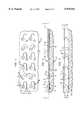
- FIG. 1is a fragmentary, diagrammatic sectional elevational view depicting first and second elements in accordance with one embodiment of the invention after connection of the leads between these elements, but prior to relative movement of these elements.
- FIG. 2is a fragmentary diagrammatic bottom view, taken along lines 2--2 in FIG. 1, depicting the first element used in the structure of FIG. 1.
- FIG. 3is a view similar to FIG. 1 but depicting the structure in a later stage of the process, during relative movement of the elements.
- FIGS. 4, 5 and 6are views similar to FIGS. 1, 2 and 3 respectively, but depicting elements in accordance with a further embodiment of the invention, FIG. 5 being taken along line 5--5 in FIG. 4.
- FIG. 7is a diagrammatic top plan view of an assembly during a process in accordance with a further embodiment of the invention.
- FIG. 8is a diagrammatic sectional view taken along line 8--8 in FIG. 7.
- FIG. 9is a view similar to FIG. 8 but depicting the assembly in a later stage of the process.
- FIG. 10is a diagrammatic sectional view of an assembly during a process according to a further embodiment of the invention.
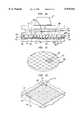
- FIG. 11is a perspective view of a wafer in accordance with a further embodiment of the invention.
- FIG. 12a fragmentary, diagrammatic view of a portion of the wafer depicted in FIG. 11.
- connection componentincludes a flexible sheet dielectric structure 11 having a bottom surface 12, a top surface 14, and a set of conductive power and ground planes extending parallel to these surfaces.
- One such conductive plane 16is visible in the drawing figures; the others (not shown) extend inside the dielectric structure or on its surfaces.
- the dielectric structure 11 of the connection componentmay include one or more sheets of a flexible but substantially inextensible dielectric material such a polyimide or other or other known dimensionally stable polymeric films used in the semiconductor industry.
- the dielectric sheetdesirably is about 25-35 microns thick.
- the conductive planesmay be formed as thin, flexible metal layers such as copper layers formed by conventional additive or subtractive plating and etching processes.
- a large number of electrically conductive signal leads 18are provided on bottom surface 12.
- Each signal leadhas a terminal end 20 and a tip end 22.
- the terminal end of each leadis permanently secured to the dielectric structure of first element 10.
- the terminal end of each leadis secured to the dielectric structure by a metallic via structure 24 extending through the first element and a terminal 26 integral with the structure 24 overlying top surface 14. Because the terminal ends of the leads are permanently attached to the dielectric structure, the terminal ends are also referred to herein as the fixed ends of the leads.
- the via structures 24 associated with the signal leadsextend through holes 30 in conductive planes 16, so that the via structures 24 and the signal leads are insulated from the conductive planes 16.
- some of the signal leads 18may be connected to the conductive planes by the via structures 24 or by other interconnecting elements (not shown).
- each leadis provided with a mass of bonding material 28.
- the tip end of each signal lead 18is releasably secured to bottom surface 12 of the dielectric sheet 11.
- the tip ends of the leadsmay be releasably attached to the bottom surface itself by adhesion between the lead material and the bottom surface of the dielectric layer, within a relatively small region disposed between the lead tip end and the bottom surface of the dielectric layer.
- the tip ends of the leadsmay be secured to the bottom surface by frangible elements or may be bonded to the bottom surface of dielectric sheet by a bonding process which provides a relatively low peel strength.
- each lead 18is curved and extends in a horizontal plane substantially parallel to the bottom surface of the dielectric layer.
- horizontalrefers to the direction parallel to the component surface.
- horizontalrefers to the directions along the confronting surfaces.
- verticalrefers to the direction transverse to the horizontal directions. Thus, in the case of components having confronting surfaces, the vertical directions are the directions from one component toward the other component.
- Each signal lead 18desirably is thin and flexible.
- the leadsmay be formed from metallic or other conductive material, alone or in conjunction with a dielectric material such as a polymeric material.
- the dimensions of the signal leadsmay be as described in the '964 patent.
- the connection componentis intended to connect with a microelectronic component having contacts in a rectilinear grid with row and column spacings of about 1000 microns
- the leadsmay be on the order of 35 microns wide, and the distance D 1 between the center of the fixed or terminal end 20 and the center of the free or tip end 22 of each lead may be on the order of 500-1000 microns.
- leads 18are curved, the length of each lead is considerably longer than the straight-line distance D 1 .
- the term "length”should be understood as referring to the shortest distance between the fixed end and the free end, measured along the lead itself. Where the lead is curved, the shortest distance along the lead itself normally will not be a straight line.
- a plurality of restraining straps 32are also provided on the bottom surface 12 of the dielectric sheet or first element 10. As shown in FIG. 2, restraining straps 32 are interspersed in the array of signal leads 18. Thus, the restraining straps are provided at intervals over the area encompassed by the array of restraining straps.
- the structure of the restraining straps 32is generally similar to the structure of signal leads 18. Thus, each restraining strap 32 has a fixed or terminal end 34 permanently fastened to the dielectric structure 11 of connection component 10 by a via structure 36 extending through the dielectric sheet and a terminal 38 on the top surface 14.
- Each restraining strap 32further has a tip end or free end 40 releasably connected to the bottom surface 12 of the dielectric sheet, each such tip end being provided with a bonding material 42.
- Most or all of the restraining straps 32are connected to the potential planes 16, as by interconnection between via structures 36 and one or more of the potential planes, or by other connecting elements (not shown). Different ones of the restraining straps 32 may be connected to different potential planes. For example, some of the restraining straps may be connected to a first potential plane which serves as a power plane whereas other restraining straps 32 may be connected to a second potential plane serving as a ground reference plane.
- the restraining straps 32are shorter than signal leads 18.
- each restraining strap 32measured along the strap itself, in the manner discussed above, is less than the length of each signal lead 18.
- restraining straps 32have larger cross-sectional areas than signal leads 18.
- the restraining strapsmay have cross-sectional areas about 1.5 times the cross-sectional areas of the signal leads or more.
- the masses of conductive bonding material 42 on the tip ends of the restraining strapsmay cover larger areas than the corresponding masses 28 on the tip ends of the signal leads.
- the restraining strapsare of stronger, more robust construction than the signal leads.
- the assemblywill include a relatively small number of restraining straps 32 and a relatively large number of signal leads 18. Therefore, any additional area consumed by providing relatively large, robust restraining straps will be minimal.
- first element or connection component 10is connected to a second element such as a semiconductor wafer 50.
- Wafer 50has signal contacts 52 and ground and power reference contacts 54 distributed over its top surface 56.
- the tip ends 22 of signal leads 18are connected to the signal contacts 52 whereas the tip ends 40 of the restraining straps 32 are connected to the reference contacts 54.
- reference contacts 54may be larger and more robust than the signal contacts 52.
- the bottom surface 12 of the first element or connection component, with the leads and straps thereon,is juxtaposed with the top surface 56 of the second element or wafer.
- the elementsare aligned with one another so as to align the tip or free end of each lead and each strap with a contact on the wafer.
- the bonding materials on the tip ends of the leadsare activated to bond the free or tip ends of the leads and straps to the contacts.
- the bonding materials 28 and 42 on the leads and strapsinclude a heat-activatable bonding material
- heatmay be applied while pressing the dielectric element 11 of the connection component toward the wafer.
- the alignment and bonding stepsmay be performed as described in the '964 patent.
- the dielectric elementmay be held taut in a rigid frame, and may be reinforced by a reinforcing element (not shown) on the top surface 14 to facilitate accurate alignment over the entire area of the dielectric element.
- first element 10 and second element 50are moved with a component of motion in a vertical direction V away from one another. This may be accomplished by injecting a fluid material such as gas or, preferably, a curable liquid 60, under pressure between the first and second elements. Movement of the first and second elements relative to one another brings the assembly to the condition illustrated in FIG. 3. In this movement, the leads 18 and straps 34 are bent vertically away from the bottom surface of the first element. Thus, the tip end 22 of each lead is moved vertically away from the terminal end 20 of the same lead. This movement is accommodated by the initial curvature of each signal lead, which is partially straightened.
- a fluid materialsuch as gas or, preferably, a curable liquid 60
- the tip ends 40 of the restraining strapsmove vertically away from the terminal ends 34 of the restraining straps.
- the vertical movement of the tip endsstraightens the initial curvature of the lead.
- Restraining straps 32reach a substantially straight, fully extended condition as illustrated in FIG. 3. In this condition, the restraining straps 32 arrest further vertical movement of first element 10 relative to second element 50. Because restraining straps 32 are shorter than signal leads 18, restraining straps 18 will reach this condition while signal leads 18 are still slack and still partially curved. Thus, the restraining straps constrain the movement of the first and second elements away from one another, and assure that such movement ceases before the signal leads are pulled taut.
- the curable liquid materialis cured to form a compliant layer such as a gel or elastomer between the two elements.
- the resulting assemblyis then severed, as by sawing the assembly to sever the dielectric element, compliant layer and wafer and form individual units.
- Each unitincludes one or more of the semiconductor chips included in the wafer or second element 50, together with the overlying portions of the connection component or first element 10.
- Each unitprovides a packaged semiconductor chip or assembly of chips, which may be mounted to a circuit board or other substrate, as by solder-bonding the terminals 26 and 38 to the substrate.
- the leads and restraining strapsprovide electrical interconnection to the substrate, but allow relative movement of the semiconductor chip and the substrate.
- the curing and severing stepscan be performed as described in greater detail in the '964 patent.
- the leadsmay be provided on the surface of either element as, for example, on the chip or wafer rather than on a dielectric sheet.
- the signal leadsmay be initially straight and the movement of the first and second elements relative to one another may include both a vertical component of motion and a horizontal component of motion.
- restraining straps in accordance with the present inventionmay be provided.
- the restraining strapswill be shorter than the signal leads.
- straight restraining straps 132 and straight signal leads 118may be provided.
- the first element 110 and second element 150are connected by bonding the free or tip ends 122 of the signal leads to signal contacts on the second element or semiconductor device 150 and by bonding the free or tip ends 140 of restraining straps 132 to contacts such as power or ground contacts on the second element 150
- all of the leadsare initially straight.
- the free or tip end 122 of each leadis offset from the terminal end 120 of the same lead in a first horizontal direction H.
- the free end 140 of each restraining strapis also offset in first horizontal direction H from the fixed end 134 of the same strap.
- the restraining straps 132are shorter than the signal leads 118.
- restraining straps 132remain taut.
- the first element 110thus moves in an arc generally as indicated by the arcuate arrow A relative to the second element.
- the restraining straps 132constrain the movement of the first element relative to the second element and constrain first element 110 to move in first horizontal direction H relative to the second element as the first element moves vertically away from the second element.
- the combined vertical and horizontal motiondeforms each of signal leads 118 into a bent, generally S-shaped configuration as shown in FIG. 6. Such horizontal motion will occur without the use of mechanical devices to move the two elements horizontally relative to one another.
- a fluidsuch as a gas or, preferably, a curable liquid encapsulant such as an elastomer 151 may be injected under pressure between the first and second elements. This pressure will force the elements away from one another in the vertical direction. The restraining straps will constrain the first element to move horizontally relative to the second element during this process.
- the restraining strapsmay be connected to "dummy" contacts on the chip or wafer, and may serve no electrical function whatsoever.
- the restraining strapscan be used to provide additional signal connections.
- the restraining strapsare formed from the same materials as the signal leads and hence the restraining straps act as electrically conductive leads.
- the restraining strapsfrom nonconductive materials such as polymers. The number of restraining straps or restraining straps and the placement of these elements on the surfaces of the elements can be varied.
- restraining strapsare dispersed at spaced apart locations over substantially the entire extent of the sheets, so that restraining straps limit vertical movement of each area of the flexible sheet.
- a flexible sheetlike elementmay be provided with a rigid reinforcing element such as a conductive metallic sheet.
- the rigid reinforcing elementAfter movement of the elements to deform the leads, and after formation of a compliant layer between the elements, the rigid reinforcing element can be etched or otherwise treated to remove metal from it and convert the reinforcing element to electrically conductive parts of the assembly such as terminals. This restores flexibility of the flexible element, and allows the terminals to move relative to one another and relative to the opposite element such as the chip or wafer.
- These techniquescan be used in the present invention.
- the flexible sheetlike elementwill not tend to bulge out of plane. Therefore, greater spacings can be provided between the restraining straps.
- both elementsare rigid and do not tend to bulge or bend, large spacings can be provided between restraining straps.
- An assembly according to a further embodiment of the inventionincludes a semiconductor chip 250 having rows of contacts 252 along its edges.
- the assemblyfurther includes a connection component 210 having a dielectric structural element 211 with terminals 226 thereon.
- signal leads 218extend horizontally outwardly, beyond edges 213 of the dielectric element.
- An inner end 220 of each signal leadis fixed to the dielectric structure and electrically connected to a terminal 226 on the dielectric element, whereas the outer or free end 222 of each lead is connected to one of the chip contacts 252.
- the assemblyfurther includes restraining straps 232, each having a fixed end 234 permanently fastened to the dielectric element and a free end 240 bonded to the chip.
- the restraining strapsare interspersed in the rows of leads.
- the restraining strapsare shorter and stronger than the leads.
- the leadsare curved.
- leads 218are curved in both the vertical and horizontal directions, and extend both vertically and horizontally.
- Leads 218may be provided as a part of the connection component, or may be formed in place by a process such as wire bonding while the connection component is in place on the chip.
- Restraining straps 232are curved, but are shorter than signal leads 218.
- the restraining strapsalso may be provided as part of the connection component or may be formed in place, as by wire bonding using a relatively heavy-gauge wire.
- the assemblyfurther includes a foamable layer 270 disposed between the dielectric element and the chip.
- the foamable layermay include a thermoplastic or other polymeric material in conjunction with a blowing agent adapted to form a gas upon exposure to heat.
- a foamable materialwill generate a gas under pressure and hence will introduce the gas under pressure between the opposed surfaces of the elements.
- the blowing agent in the foamable materialmay be a heat-activated agent.
- foamable layer 270is activated.
- the blowing agentintroduces a gas under pressure between chip 250 and connection component 210, thus forcing the two elements vertically away from one another and deforming leads 218 to a more vertically-extensive disposition.
- the restraining strapsarrest the vertical movement of the elements away from one another before the signal leads are pulled taut.
- the fixed ends of the leads and strapsmay be securely bonded to the dielectric structure itself.
- the leads and strapsmay be electrically connected to traces or to other parts of the connection component which do not mechanically secure the fixed ends.
- the strapsmay be formed integrally with potential reference planes such as ground or power planes in connection component.
- the methods and components according to the FIGS. 1-6can be used with single chips, rather than with a wafer. Both elements may includes chips or wafers.
- the present inventioncan be applied to connect two chips to one another.
- the methods and components discussed abovecan be used with assemblies of plural chips, which may remain united in the finished device to form a multichip module.
- the connection component and leadsmay serve to interconnect the chips in the module.
- the elementsmay include microelectronic elements other than chips or wafers.
- one element 310is itself an assemblage including a package element 312 in the form of a metallic can having a flange 314 at its periphery, and further including a semiconductor chip 316 and additional electrical elements 318 such as capacitors, inductors, resistors or additional semiconductor chips.
- the chip and other electrical elementshave front surfaces 322 substantially coplanar with the front surface 324 of flange 314.
- the front surfaces of the flange, together with the front surfaces of the chip and of the other electrical elementscooperatively define the front surface of element 310.
- the other element 350is a connection component including a flexible dielectric sheet 352 and one or more metallic potential planes 354. Only one such potential plane is partially shown in FIG. 10.
- Connection component 350further includes interconnect leads 356 extending along one or both surfaces of the dielectric sheet, or disposed within the sheet, and also includes terminals 358. Although only a few such leads and terminals are depicted in FIG. 10, numerous leads would be provided in actual practice.
- Flexible signal leads 360are connected between connection component 350 and the chip 316 and other electrical components 318 of assemblage 310.
- the restraining straps 362are provided only adjacent the periphery of the connection component, and are connected between a potential plane 354 of the connection component and the flange 314 of the package.
- the terminals and leadsmay be arranged to provide a "fan-out" arrangement, wherein the terminals 358 are disposed over a surface area larger than the area of chip 316.
- the interconnect leads 356 and signal leads 360may be arranged to connect the various electrical components to one another and to the appropriate terminals 358.
- the terminals 358 of the connection componentare disposed in engagement with a flat surface such as a support 370.
- Package 312is urged toward the support by a weight 372 or other device for applying a force in the vertical direction without impeding horizontal movement of the package.
- a fluidsuch as a liquid encapsulant or foam is provided under pressure between assembly 310 and connection component 350, causing these elements to move vertically away from one another.
- the restraining straps 362constrain the relative motion of the elements.
- the restraining strapslimit vertical movement of the elements, and cause horizontal movement of the elements relative to one another.
- Support 370maintains coplanarity of the terminals 358, and limits bulging of the flexible dielectric member 352.
- the structural element which bears the leads and straps prior to assemblymay be a semiconductor chip, wafer or other assemblage of plural chips.
- a unitary semiconductor wafer 401(FIG. 11) includes a plurality of chips 403. Each chip has numerous signal leads 405 (FIG. 12) and restraining straps 407 disposed on the top, contact-bearing surface of the chip.
- the signal leads and strapshave fixed ends connected to the structural element or wafer 401.
- the signal leadsare connected to signal contacts of each chip, and hence are connected to internal signal connections 411 within the chip.
- the restraining straps 407are connected to constant-potential connections or reference contacts 409 such as power or ground connections.
- the free ends of the leads and strapsare releasably secured to the structural element.
- the wafermay have a layer of a polymer such as polyimide on its top surfaces, and the leads and straps may be connected to the wafer in the same manner as discussed above with reference to leads connected to a dielectric film.
Landscapes
- Physics & Mathematics (AREA)
- Engineering & Computer Science (AREA)
- Computer Hardware Design (AREA)
- Microelectronics & Electronic Packaging (AREA)
- Power Engineering (AREA)
- Condensed Matter Physics & Semiconductors (AREA)
- General Physics & Mathematics (AREA)
- Geometry (AREA)
- Wire Bonding (AREA)
Abstract
Description
Claims (20)
Priority Applications (3)
| Application Number | Priority Date | Filing Date | Title |
|---|---|---|---|
| US08/989,582US5976913A (en) | 1996-12-12 | 1997-12-12 | Microelectronic mounting with multiple lead deformation using restraining straps |
| US09/385,320US6208024B1 (en) | 1996-12-12 | 1999-08-30 | Microelectronic mounting with multiple lead deformation using restraining straps |
| US09/791,245US6362520B2 (en) | 1996-12-12 | 2001-02-22 | Microelectronic mounting with multiple lead deformation using restraining straps |
Applications Claiming Priority (3)
| Application Number | Priority Date | Filing Date | Title |
|---|---|---|---|
| US3306696P | 1996-12-12 | 1996-12-12 | |
| US4569097P | 1997-05-06 | 1997-05-06 | |
| US08/989,582US5976913A (en) | 1996-12-12 | 1997-12-12 | Microelectronic mounting with multiple lead deformation using restraining straps |
Related Child Applications (1)
| Application Number | Title | Priority Date | Filing Date |
|---|---|---|---|
| US09/385,320DivisionUS6208024B1 (en) | 1996-12-12 | 1999-08-30 | Microelectronic mounting with multiple lead deformation using restraining straps |
Publications (1)
| Publication Number | Publication Date |
|---|---|
| US5976913Atrue US5976913A (en) | 1999-11-02 |
Family
ID=27364298
Family Applications (3)
| Application Number | Title | Priority Date | Filing Date |
|---|---|---|---|
| US08/989,582Expired - LifetimeUS5976913A (en) | 1996-12-12 | 1997-12-12 | Microelectronic mounting with multiple lead deformation using restraining straps |
| US09/385,320Expired - LifetimeUS6208024B1 (en) | 1996-12-12 | 1999-08-30 | Microelectronic mounting with multiple lead deformation using restraining straps |
| US09/791,245Expired - LifetimeUS6362520B2 (en) | 1996-12-12 | 2001-02-22 | Microelectronic mounting with multiple lead deformation using restraining straps |
Family Applications After (2)
| Application Number | Title | Priority Date | Filing Date |
|---|---|---|---|
| US09/385,320Expired - LifetimeUS6208024B1 (en) | 1996-12-12 | 1999-08-30 | Microelectronic mounting with multiple lead deformation using restraining straps |
| US09/791,245Expired - LifetimeUS6362520B2 (en) | 1996-12-12 | 2001-02-22 | Microelectronic mounting with multiple lead deformation using restraining straps |
Country Status (1)
| Country | Link |
|---|---|
| US (3) | US5976913A (en) |
Cited By (24)
| Publication number | Priority date | Publication date | Assignee | Title |
|---|---|---|---|---|
| US6380060B1 (en) | 2000-03-08 | 2002-04-30 | Tessera, Inc. | Off-center solder ball attach and methods therefor |
| US6486547B2 (en) | 1995-09-18 | 2002-11-26 | Tessera, Inc. | Microelectronic assembly incorporating lead regions defined by gaps in a polymeric sheet |
| US6495462B1 (en)* | 1998-02-09 | 2002-12-17 | Tessera, Inc. | Components with releasable leads |
| US20030048624A1 (en)* | 2001-08-22 | 2003-03-13 | Tessera, Inc. | Low-height multi-component assemblies |
| US6589819B2 (en) | 2000-09-29 | 2003-07-08 | Tessera, Inc. | Microelectronic packages having an array of resilient leads and methods therefor |
| US6627483B2 (en)* | 1998-12-04 | 2003-09-30 | Formfactor, Inc. | Method for mounting an electronic component |
| US6657286B2 (en) | 2000-09-21 | 2003-12-02 | Tessera, Inc. | Microelectronic assembly formation with lead displacement |
| US6664621B2 (en) | 2000-05-08 | 2003-12-16 | Tessera, Inc. | Semiconductor chip package with interconnect structure |
| US20040032011A1 (en)* | 2001-08-28 | 2004-02-19 | Tessera, Inc. | Microelectronic assemblies incorporating inductors |
| US6713374B2 (en)* | 1999-07-30 | 2004-03-30 | Formfactor, Inc. | Interconnect assemblies and methods |
| US6737265B2 (en) | 1994-07-07 | 2004-05-18 | Tessera, Inc. | Microelectronic unit forming methods and materials |
| US20040159959A1 (en)* | 2000-03-15 | 2004-08-19 | Masud Beroz | Assemblies for temporarily connecting microelectronic elements for testing and methods therefor |
| US20040238857A1 (en)* | 2001-08-28 | 2004-12-02 | Tessera, Inc. | High frequency chip packages with connecting elements |
| US20050017348A1 (en)* | 2003-02-25 | 2005-01-27 | Tessera, Inc. | Manufacture of mountable capped chips |
| US6885106B1 (en) | 2001-01-11 | 2005-04-26 | Tessera, Inc. | Stacked microelectronic assemblies and methods of making same |
| US7224056B2 (en) | 2003-09-26 | 2007-05-29 | Tessera, Inc. | Back-face and edge interconnects for lidded package |
| US7265440B2 (en) | 2003-06-16 | 2007-09-04 | Tessera Technologies Hungary Kft. | Methods and apparatus for packaging integrated circuit devices |
| US7435108B1 (en) | 1999-07-30 | 2008-10-14 | Formfactor, Inc. | Variable width resilient conductive contact structures |
| US7479398B2 (en) | 2003-07-03 | 2009-01-20 | Tessera Technologies Hungary Kft. | Methods and apparatus for packaging integrated circuit devices |
| US7936062B2 (en) | 2006-01-23 | 2011-05-03 | Tessera Technologies Ireland Limited | Wafer level chip packaging |
| US7960272B2 (en) | 2002-10-24 | 2011-06-14 | Megica Corporation | Method for fabricating thermal compliant semiconductor chip wiring structure for chip scale packaging |
| US8101459B2 (en)* | 2001-08-24 | 2012-01-24 | Micron Technology, Inc. | Methods for assembling semiconductor devices in stacked arrangements by positioning spacers therebetween |
| US8143095B2 (en) | 2005-03-22 | 2012-03-27 | Tessera, Inc. | Sequential fabrication of vertical conductive interconnects in capped chips |
| US8604605B2 (en) | 2007-01-05 | 2013-12-10 | Invensas Corp. | Microelectronic assembly with multi-layer support structure |
Families Citing this family (54)
| Publication number | Priority date | Publication date | Assignee | Title |
|---|---|---|---|---|
| US6313523B1 (en)* | 1999-10-28 | 2001-11-06 | Hewlett-Packard Company | IC die power connection using canted coil spring |
| US20030205828A9 (en)* | 2001-04-05 | 2003-11-06 | Larry Kinsman | Circuit substrates, semiconductor packages, and ball grid arrays |
| DE10137666A1 (en)* | 2001-08-01 | 2003-02-27 | Infineon Technologies Ag | Protection device for assemblies and process for their manufacture |
| KR101313391B1 (en) | 2004-11-03 | 2013-10-01 | 테세라, 인코포레이티드 | Stacked packaging improvements |
| US8058101B2 (en)* | 2005-12-23 | 2011-11-15 | Tessera, Inc. | Microelectronic packages and methods therefor |
| US8487428B2 (en)* | 2007-11-20 | 2013-07-16 | Fujitsu Limited | Method and system for providing a reliable semiconductor assembly |
| US8084348B2 (en)* | 2008-06-04 | 2011-12-27 | Oracle America, Inc. | Contact pads for silicon chip packages |
| US8278752B2 (en)* | 2009-12-23 | 2012-10-02 | Intel Corporation | Microelectronic package and method for a compression-based mid-level interconnect |
| US8407888B2 (en) | 2010-05-07 | 2013-04-02 | Oracle International Corporation | Method of assembling a circuit board assembly |
| US8482111B2 (en) | 2010-07-19 | 2013-07-09 | Tessera, Inc. | Stackable molded microelectronic packages |
| US9159708B2 (en) | 2010-07-19 | 2015-10-13 | Tessera, Inc. | Stackable molded microelectronic packages with area array unit connectors |
| KR101075241B1 (en) | 2010-11-15 | 2011-11-01 | 테세라, 인코포레이티드 | Microelectronic package with terminals in dielectric member |
| US20120146206A1 (en) | 2010-12-13 | 2012-06-14 | Tessera Research Llc | Pin attachment |
| KR101128063B1 (en) | 2011-05-03 | 2012-04-23 | 테세라, 인코포레이티드 | Package-on-package assembly with wire bonds to encapsulation surface |
| US8618659B2 (en) | 2011-05-03 | 2013-12-31 | Tessera, Inc. | Package-on-package assembly with wire bonds to encapsulation surface |
| US8836136B2 (en) | 2011-10-17 | 2014-09-16 | Invensas Corporation | Package-on-package assembly with wire bond vias |
| US8946757B2 (en) | 2012-02-17 | 2015-02-03 | Invensas Corporation | Heat spreading substrate with embedded interconnects |
| US8372741B1 (en) | 2012-02-24 | 2013-02-12 | Invensas Corporation | Method for package-on-package assembly with wire bonds to encapsulation surface |
| US9349706B2 (en) | 2012-02-24 | 2016-05-24 | Invensas Corporation | Method for package-on-package assembly with wire bonds to encapsulation surface |
| US8835228B2 (en) | 2012-05-22 | 2014-09-16 | Invensas Corporation | Substrate-less stackable package with wire-bond interconnect |
| US9391008B2 (en) | 2012-07-31 | 2016-07-12 | Invensas Corporation | Reconstituted wafer-level package DRAM |
| US9502390B2 (en) | 2012-08-03 | 2016-11-22 | Invensas Corporation | BVA interposer |
| US8975738B2 (en) | 2012-11-12 | 2015-03-10 | Invensas Corporation | Structure for microelectronic packaging with terminals on dielectric mass |
| US8878353B2 (en) | 2012-12-20 | 2014-11-04 | Invensas Corporation | Structure for microelectronic packaging with bond elements to encapsulation surface |
| US9136254B2 (en) | 2013-02-01 | 2015-09-15 | Invensas Corporation | Microelectronic package having wire bond vias and stiffening layer |
| US8883563B1 (en) | 2013-07-15 | 2014-11-11 | Invensas Corporation | Fabrication of microelectronic assemblies having stack terminals coupled by connectors extending through encapsulation |
| US9023691B2 (en) | 2013-07-15 | 2015-05-05 | Invensas Corporation | Microelectronic assemblies with stack terminals coupled by connectors extending through encapsulation |
| US9034696B2 (en) | 2013-07-15 | 2015-05-19 | Invensas Corporation | Microelectronic assemblies having reinforcing collars on connectors extending through encapsulation |
| US9167710B2 (en) | 2013-08-07 | 2015-10-20 | Invensas Corporation | Embedded packaging with preformed vias |
| US9685365B2 (en) | 2013-08-08 | 2017-06-20 | Invensas Corporation | Method of forming a wire bond having a free end |
| US20150076714A1 (en) | 2013-09-16 | 2015-03-19 | Invensas Corporation | Microelectronic element with bond elements to encapsulation surface |
| US9087815B2 (en) | 2013-11-12 | 2015-07-21 | Invensas Corporation | Off substrate kinking of bond wire |
| US9082753B2 (en) | 2013-11-12 | 2015-07-14 | Invensas Corporation | Severing bond wire by kinking and twisting |
| US9583456B2 (en) | 2013-11-22 | 2017-02-28 | Invensas Corporation | Multiple bond via arrays of different wire heights on a same substrate |
| US9263394B2 (en) | 2013-11-22 | 2016-02-16 | Invensas Corporation | Multiple bond via arrays of different wire heights on a same substrate |
| US9379074B2 (en) | 2013-11-22 | 2016-06-28 | Invensas Corporation | Die stacks with one or more bond via arrays of wire bond wires and with one or more arrays of bump interconnects |
| US9583411B2 (en) | 2014-01-17 | 2017-02-28 | Invensas Corporation | Fine pitch BVA using reconstituted wafer with area array accessible for testing |
| US9214454B2 (en) | 2014-03-31 | 2015-12-15 | Invensas Corporation | Batch process fabrication of package-on-package microelectronic assemblies |
| US10381326B2 (en) | 2014-05-28 | 2019-08-13 | Invensas Corporation | Structure and method for integrated circuits packaging with increased density |
| US9646917B2 (en) | 2014-05-29 | 2017-05-09 | Invensas Corporation | Low CTE component with wire bond interconnects |
| US9412714B2 (en) | 2014-05-30 | 2016-08-09 | Invensas Corporation | Wire bond support structure and microelectronic package including wire bonds therefrom |
| US9735084B2 (en) | 2014-12-11 | 2017-08-15 | Invensas Corporation | Bond via array for thermal conductivity |
| US9888579B2 (en)* | 2015-03-05 | 2018-02-06 | Invensas Corporation | Pressing of wire bond wire tips to provide bent-over tips |
| US9502372B1 (en) | 2015-04-30 | 2016-11-22 | Invensas Corporation | Wafer-level packaging using wire bond wires in place of a redistribution layer |
| US9761554B2 (en) | 2015-05-07 | 2017-09-12 | Invensas Corporation | Ball bonding metal wire bond wires to metal pads |
| US10490528B2 (en) | 2015-10-12 | 2019-11-26 | Invensas Corporation | Embedded wire bond wires |
| US9490222B1 (en) | 2015-10-12 | 2016-11-08 | Invensas Corporation | Wire bond wires for interference shielding |
| US10332854B2 (en) | 2015-10-23 | 2019-06-25 | Invensas Corporation | Anchoring structure of fine pitch bva |
| US10181457B2 (en) | 2015-10-26 | 2019-01-15 | Invensas Corporation | Microelectronic package for wafer-level chip scale packaging with fan-out |
| US10043779B2 (en) | 2015-11-17 | 2018-08-07 | Invensas Corporation | Packaged microelectronic device for a package-on-package device |
| US9659848B1 (en) | 2015-11-18 | 2017-05-23 | Invensas Corporation | Stiffened wires for offset BVA |
| US9984992B2 (en) | 2015-12-30 | 2018-05-29 | Invensas Corporation | Embedded wire bond wires for vertical integration with separate surface mount and wire bond mounting surfaces |
| US9935075B2 (en) | 2016-07-29 | 2018-04-03 | Invensas Corporation | Wire bonding method and apparatus for electromagnetic interference shielding |
| US10299368B2 (en) | 2016-12-21 | 2019-05-21 | Invensas Corporation | Surface integrated waveguides and circuit structures therefor |
Citations (2)
| Publication number | Priority date | Publication date | Assignee | Title |
|---|---|---|---|---|
| US5518964A (en)* | 1994-07-07 | 1996-05-21 | Tessera, Inc. | Microelectronic mounting with multiple lead deformation and bonding |
| US5688716A (en)* | 1994-07-07 | 1997-11-18 | Tessera, Inc. | Fan-out semiconductor chip assembly |
Family Cites Families (5)
| Publication number | Priority date | Publication date | Assignee | Title |
|---|---|---|---|---|
| JPH03263109A (en)* | 1990-03-14 | 1991-11-22 | Hitachi Ltd | Computer implementation structure |
| JP3263109B2 (en) | 1991-12-26 | 2002-03-04 | 日本電産株式会社 | Spindle motor |
| US5763941A (en)* | 1995-10-24 | 1998-06-09 | Tessera, Inc. | Connection component with releasable leads |
| US5937276A (en)* | 1996-12-13 | 1999-08-10 | Tessera, Inc. | Bonding lead structure with enhanced encapsulation |
| US6063648A (en)* | 1998-10-29 | 2000-05-16 | Tessera, Inc. | Lead formation usings grids |
- 1997
- 1997-12-12USUS08/989,582patent/US5976913A/ennot_activeExpired - Lifetime
- 1999
- 1999-08-30USUS09/385,320patent/US6208024B1/ennot_activeExpired - Lifetime
- 2001
- 2001-02-22USUS09/791,245patent/US6362520B2/ennot_activeExpired - Lifetime
Patent Citations (2)
| Publication number | Priority date | Publication date | Assignee | Title |
|---|---|---|---|---|
| US5518964A (en)* | 1994-07-07 | 1996-05-21 | Tessera, Inc. | Microelectronic mounting with multiple lead deformation and bonding |
| US5688716A (en)* | 1994-07-07 | 1997-11-18 | Tessera, Inc. | Fan-out semiconductor chip assembly |
Cited By (48)
| Publication number | Priority date | Publication date | Assignee | Title |
|---|---|---|---|---|
| US6737265B2 (en) | 1994-07-07 | 2004-05-18 | Tessera, Inc. | Microelectronic unit forming methods and materials |
| US6486547B2 (en) | 1995-09-18 | 2002-11-26 | Tessera, Inc. | Microelectronic assembly incorporating lead regions defined by gaps in a polymeric sheet |
| US6495462B1 (en)* | 1998-02-09 | 2002-12-17 | Tessera, Inc. | Components with releasable leads |
| US6627483B2 (en)* | 1998-12-04 | 2003-09-30 | Formfactor, Inc. | Method for mounting an electronic component |
| US20070269909A1 (en)* | 1998-12-04 | 2007-11-22 | Formfactor, Inc. | Method for processing an integrated circuit |
| US7217580B2 (en) | 1998-12-04 | 2007-05-15 | Formfactor Inc. | Method for processing an integrated circuit |
| US6644982B1 (en) | 1998-12-04 | 2003-11-11 | Formfactor, Inc. | Method and apparatus for the transport and tracking of an electronic component |
| US20090035959A1 (en)* | 1999-07-30 | 2009-02-05 | Formfactor, Inc. | Interconnect assemblies and methods |
| US6713374B2 (en)* | 1999-07-30 | 2004-03-30 | Formfactor, Inc. | Interconnect assemblies and methods |
| US7435108B1 (en) | 1999-07-30 | 2008-10-14 | Formfactor, Inc. | Variable width resilient conductive contact structures |
| US20020117761A1 (en)* | 2000-03-08 | 2002-08-29 | Wael Zohni | Off-center solder ball attach assembly |
| US6380060B1 (en) | 2000-03-08 | 2002-04-30 | Tessera, Inc. | Off-center solder ball attach and methods therefor |
| US6870267B2 (en) | 2000-03-08 | 2005-03-22 | Tessera, Inc. | Off-center solder ball attach assembly |
| US7205659B2 (en) | 2000-03-15 | 2007-04-17 | Tessera, Inc. | Assemblies for temporarily connecting microelectronic elements for testing and methods therefor |
| US20040159959A1 (en)* | 2000-03-15 | 2004-08-19 | Masud Beroz | Assemblies for temporarily connecting microelectronic elements for testing and methods therefor |
| US6794202B2 (en) | 2000-03-15 | 2004-09-21 | Tessera, Inc. | Assemblies for temporarily connecting microelectronic elements for testing and methods therefor |
| US20040077129A1 (en)* | 2000-05-08 | 2004-04-22 | Tessera, Inc. | Semiconductor chip package with interconnect structure |
| US6664621B2 (en) | 2000-05-08 | 2003-12-16 | Tessera, Inc. | Semiconductor chip package with interconnect structure |
| US6921713B2 (en) | 2000-05-08 | 2005-07-26 | Tessera, Inc. | Semiconductor chip package with interconnect structure |
| US6657286B2 (en) | 2000-09-21 | 2003-12-02 | Tessera, Inc. | Microelectronic assembly formation with lead displacement |
| US6589819B2 (en) | 2000-09-29 | 2003-07-08 | Tessera, Inc. | Microelectronic packages having an array of resilient leads and methods therefor |
| US20030173107A1 (en)* | 2000-09-29 | 2003-09-18 | Tessera, Inc. | Microelectronic packages having an array of resilient leads |
| US6891255B2 (en) | 2000-09-29 | 2005-05-10 | Tessera, Inc. | Microelectronic packages having an array of resilient leads |
| US6885106B1 (en) | 2001-01-11 | 2005-04-26 | Tessera, Inc. | Stacked microelectronic assemblies and methods of making same |
| US20030048624A1 (en)* | 2001-08-22 | 2003-03-13 | Tessera, Inc. | Low-height multi-component assemblies |
| US8101459B2 (en)* | 2001-08-24 | 2012-01-24 | Micron Technology, Inc. | Methods for assembling semiconductor devices in stacked arrangements by positioning spacers therebetween |
| US20040238857A1 (en)* | 2001-08-28 | 2004-12-02 | Tessera, Inc. | High frequency chip packages with connecting elements |
| US20040238934A1 (en)* | 2001-08-28 | 2004-12-02 | Tessera, Inc. | High-frequency chip packages |
| US20060113645A1 (en)* | 2001-08-28 | 2006-06-01 | Tessera, Inc. | Microelectronic assemblies incorporating inductors |
| US7012323B2 (en) | 2001-08-28 | 2006-03-14 | Tessera, Inc. | Microelectronic assemblies incorporating inductors |
| US20040032011A1 (en)* | 2001-08-28 | 2004-02-19 | Tessera, Inc. | Microelectronic assemblies incorporating inductors |
| US7176506B2 (en) | 2001-08-28 | 2007-02-13 | Tessera, Inc. | High frequency chip packages with connecting elements |
| US7268426B2 (en) | 2001-08-28 | 2007-09-11 | Tessera, Inc. | High-frequency chip packages |
| US6856007B2 (en) | 2001-08-28 | 2005-02-15 | Tessera, Inc. | High-frequency chip packages |
| US7566955B2 (en) | 2001-08-28 | 2009-07-28 | Tessera, Inc. | High-frequency chip packages |
| US7960272B2 (en) | 2002-10-24 | 2011-06-14 | Megica Corporation | Method for fabricating thermal compliant semiconductor chip wiring structure for chip scale packaging |
| US8334588B2 (en) | 2002-10-24 | 2012-12-18 | Megica Corporation | Circuit component with conductive layer structure |
| US20050017348A1 (en)* | 2003-02-25 | 2005-01-27 | Tessera, Inc. | Manufacture of mountable capped chips |
| US7754537B2 (en) | 2003-02-25 | 2010-07-13 | Tessera, Inc. | Manufacture of mountable capped chips |
| US7642629B2 (en) | 2003-06-16 | 2010-01-05 | Tessera Technologies Hungary Kft. | Methods and apparatus for packaging integrated circuit devices |
| US7265440B2 (en) | 2003-06-16 | 2007-09-04 | Tessera Technologies Hungary Kft. | Methods and apparatus for packaging integrated circuit devices |
| US7479398B2 (en) | 2003-07-03 | 2009-01-20 | Tessera Technologies Hungary Kft. | Methods and apparatus for packaging integrated circuit devices |
| US7495341B2 (en) | 2003-07-03 | 2009-02-24 | Tessera Technologies Hungary Kft. | Methods and apparatus for packaging integrated circuit devices |
| US7224056B2 (en) | 2003-09-26 | 2007-05-29 | Tessera, Inc. | Back-face and edge interconnects for lidded package |
| US8143095B2 (en) | 2005-03-22 | 2012-03-27 | Tessera, Inc. | Sequential fabrication of vertical conductive interconnects in capped chips |
| US7936062B2 (en) | 2006-01-23 | 2011-05-03 | Tessera Technologies Ireland Limited | Wafer level chip packaging |
| US8604605B2 (en) | 2007-01-05 | 2013-12-10 | Invensas Corp. | Microelectronic assembly with multi-layer support structure |
| US9548145B2 (en) | 2007-01-05 | 2017-01-17 | Invensas Corporation | Microelectronic assembly with multi-layer support structure |
Also Published As
| Publication number | Publication date |
|---|---|
| US6362520B2 (en) | 2002-03-26 |
| US6208024B1 (en) | 2001-03-27 |
| US20010007370A1 (en) | 2001-07-12 |
Similar Documents
| Publication | Publication Date | Title |
|---|---|---|
| US5976913A (en) | Microelectronic mounting with multiple lead deformation using restraining straps | |
| US6848173B2 (en) | Microelectric packages having deformed bonded leads and methods therefor | |
| US6175159B1 (en) | Semiconductor package | |
| US6437428B1 (en) | Ball grid array type semiconductor package having a flexible substrate | |
| US6825552B2 (en) | Connection components with anisotropic conductive material interconnection | |
| US6521480B1 (en) | Method for making a semiconductor chip package | |
| US5148265A (en) | Semiconductor chip assemblies with fan-in leads | |
| US6927095B2 (en) | Low cost and compliant microelectronic packages for high I/O and fine pitch | |
| KR20070085700A (en) | Stacked packaging improvements | |
| US6891255B2 (en) | Microelectronic packages having an array of resilient leads | |
| US7365439B2 (en) | Semiconductor device, semiconductor package for use therein, and manufacturing method thereof | |
| US6353326B2 (en) | Test carrier with molded interconnect for testing semiconductor components | |
| US6037662A (en) | Chip scale package | |
| KR100614431B1 (en) | Structure and method for manufacturing semiconductor package device of improved yield | |
| US6320250B1 (en) | Semiconductor package and process for manufacturing the same | |
| KR19980070675A (en) | Semiconductor package having offset die pad and manufacturing method thereof | |
| US20010015489A1 (en) | Semiconductor device and its manufacturing method |
Legal Events
| Date | Code | Title | Description |
|---|---|---|---|
| AS | Assignment | Owner name:TESSERA, INC., CALIFORNIA Free format text:ASSIGNMENT OF ASSIGNORS INTEREST;ASSIGNOR:DISTEFANO, THOMAS H.;REEL/FRAME:009124/0409 Effective date:19980325 | |
| AS | Assignment | Owner name:TESSERA, INC., CALIFORNIA Free format text:ASSIGNMENT OF ASSIGNORS INTEREST;ASSIGNOR:DISTEFANO, THOMAS H.;REEL/FRAME:009198/0244 Effective date:19980428 | |
| STCF | Information on status: patent grant | Free format text:PATENTED CASE | |
| FPAY | Fee payment | Year of fee payment:4 | |
| REMI | Maintenance fee reminder mailed | ||
| FPAY | Fee payment | Year of fee payment:8 | |
| FPAY | Fee payment | Year of fee payment:12 | |
| AS | Assignment | Owner name:ROYAL BANK OF CANADA, AS COLLATERAL AGENT, CANADA Free format text:SECURITY INTEREST;ASSIGNORS:INVENSAS CORPORATION;TESSERA, INC.;TESSERA ADVANCED TECHNOLOGIES, INC.;AND OTHERS;REEL/FRAME:040797/0001 Effective date:20161201 | |
| AS | Assignment | Owner name:INVENSAS CORPORATION, CALIFORNIA Free format text:RELEASE BY SECURED PARTY;ASSIGNOR:ROYAL BANK OF CANADA;REEL/FRAME:052920/0001 Effective date:20200601 Owner name:TESSERA ADVANCED TECHNOLOGIES, INC, CALIFORNIA Free format text:RELEASE BY SECURED PARTY;ASSIGNOR:ROYAL BANK OF CANADA;REEL/FRAME:052920/0001 Effective date:20200601 Owner name:FOTONATION CORPORATION (F/K/A DIGITALOPTICS CORPORATION AND F/K/A DIGITALOPTICS CORPORATION MEMS), CALIFORNIA Free format text:RELEASE BY SECURED PARTY;ASSIGNOR:ROYAL BANK OF CANADA;REEL/FRAME:052920/0001 Effective date:20200601 Owner name:INVENSAS BONDING TECHNOLOGIES, INC. (F/K/A ZIPTRONIX, INC.), CALIFORNIA Free format text:RELEASE BY SECURED PARTY;ASSIGNOR:ROYAL BANK OF CANADA;REEL/FRAME:052920/0001 Effective date:20200601 Owner name:DTS, INC., CALIFORNIA Free format text:RELEASE BY SECURED PARTY;ASSIGNOR:ROYAL BANK OF CANADA;REEL/FRAME:052920/0001 Effective date:20200601 Owner name:PHORUS, INC., CALIFORNIA Free format text:RELEASE BY SECURED PARTY;ASSIGNOR:ROYAL BANK OF CANADA;REEL/FRAME:052920/0001 Effective date:20200601 Owner name:IBIQUITY DIGITAL CORPORATION, MARYLAND Free format text:RELEASE BY SECURED PARTY;ASSIGNOR:ROYAL BANK OF CANADA;REEL/FRAME:052920/0001 Effective date:20200601 Owner name:TESSERA, INC., CALIFORNIA Free format text:RELEASE BY SECURED PARTY;ASSIGNOR:ROYAL BANK OF CANADA;REEL/FRAME:052920/0001 Effective date:20200601 Owner name:DTS LLC, CALIFORNIA Free format text:RELEASE BY SECURED PARTY;ASSIGNOR:ROYAL BANK OF CANADA;REEL/FRAME:052920/0001 Effective date:20200601 |