US5973568A - Power amplifier output module for dual-mode digital systems - Google Patents
Power amplifier output module for dual-mode digital systemsDownload PDFInfo
- Publication number
- US5973568A US5973568AUS09/088,356US8835698AUS5973568AUS 5973568 AUS5973568 AUS 5973568AUS 8835698 AUS8835698 AUS 8835698AUS 5973568 AUS5973568 AUS 5973568A
- Authority
- US
- United States
- Prior art keywords
- power amplifier
- drive circuit
- impedance matching
- matching network
- amplifier drive
- Prior art date
- Legal status (The legal status is an assumption and is not a legal conclusion. Google has not performed a legal analysis and makes no representation as to the accuracy of the status listed.)
- Expired - Lifetime
Links
Images


Classifications
- H—ELECTRICITY
- H04—ELECTRIC COMMUNICATION TECHNIQUE
- H04B—TRANSMISSION
- H04B1/00—Details of transmission systems, not covered by a single one of groups H04B3/00 - H04B13/00; Details of transmission systems not characterised by the medium used for transmission
- H04B1/02—Transmitters
- H04B1/04—Circuits
- H04B1/0483—Transmitters with multiple parallel paths
- H—ELECTRICITY
- H03—ELECTRONIC CIRCUITRY
- H03F—AMPLIFIERS
- H03F3/00—Amplifiers with only discharge tubes or only semiconductor devices as amplifying elements
- H03F3/20—Power amplifiers, e.g. Class B amplifiers, Class C amplifiers
- H03F3/24—Power amplifiers, e.g. Class B amplifiers, Class C amplifiers of transmitter output stages
- H—ELECTRICITY
- H03—ELECTRONIC CIRCUITRY
- H03F—AMPLIFIERS
- H03F3/00—Amplifiers with only discharge tubes or only semiconductor devices as amplifying elements
- H03F3/60—Amplifiers in which coupling networks have distributed constants, e.g. with waveguide resonators
- H03F3/602—Combinations of several amplifiers
- H—ELECTRICITY
- H04—ELECTRIC COMMUNICATION TECHNIQUE
- H04B—TRANSMISSION
- H04B1/00—Details of transmission systems, not covered by a single one of groups H04B3/00 - H04B13/00; Details of transmission systems not characterised by the medium used for transmission
- H04B1/005—Details of transmission systems, not covered by a single one of groups H04B3/00 - H04B13/00; Details of transmission systems not characterised by the medium used for transmission adapting radio receivers, transmitters andtransceivers for operation on two or more bands, i.e. frequency ranges
- H—ELECTRICITY
- H04—ELECTRIC COMMUNICATION TECHNIQUE
- H04B—TRANSMISSION
- H04B1/00—Details of transmission systems, not covered by a single one of groups H04B3/00 - H04B13/00; Details of transmission systems not characterised by the medium used for transmission
- H04B1/02—Transmitters
- H04B1/04—Circuits
- H04B1/0458—Arrangements for matching and coupling between power amplifier and antenna or between amplifying stages
Definitions
- This inventionrelates to internal radio architecture for telecommunication devices, and more particularly to a power amplifier output module for dual band digital systems.
- FIG. 1shows a block diagram of a radio architecture for a dual band cellular telephone in accordance with the prior art 100 is provided.
- a radio transmit signal from a first band(Band #1) will pass through a driver 102, a power amplifier 104, an impedance matching network 106, a directional coupler 108, a harmonic filter 110.
- the signalwill pass through a diplexer 112, and finally out the antenna 114.
- a radio transmit signal from a second band(Band #2) will pass through another driver 202, another power amplifier 204, another impedance matching network 206, another directional coupler 208, and another harmonic filter 210.
- the second signalwill then pass through the diplexer 112, and finally out the antenna 114.
- each of the bandshave their own dedicated components.
- Each bandhas it's own impedance matching network, directional coupler, and harmonic filter.
- Such duplication of componentsmay lead to a cellular telephone having additional circuitry, a high parts count, increased switching and power consumption, as well as increased volume, weight, and size.
- a radio architecture designwhich provides a power amplifier output module for dual mode digital systems in a monolithic component and which integrates harmonic filtering requirements into an impedance matching network and which is capable of handling two discrete power amplifier drive circuits using a single coupler and a single antenna in a highly integrated multilayer ceramic package and which provides improved insertion loss and self-shielding properties would be considered an improvement in the art.
- FIG. 1shows a block diagram of a dual band front end radio design in accordance with the prior art.
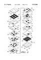
- FIG. 2shows a block diagram of a power amplifier output module for dual mode digital systems in accordance with the present invention.
- FIG. 3shows a exploded view of a multilayer package which forms the power amplifier output module for dual mode digital systems in accordance with the present invention.
- FIG. 4.shows a circuit diagram of the integrated impedance matching network/harmonic filter in accordance with the present invention.
- FIG. 5shows a frequency response curve incorporating the prior art design (dashed line) and a frequency response curve for the power amplifier output module for dual mode digital systems in accordance with the present invention.
- the power amplifier output module of the present inventionis less lossy at higher frequencies relative to the prior art manufacturing technique which involves a circuit with discrete components mounted to traditional substrates (e.g. FR-4).
- the integrated module of the present designalso provides fewer interconnections which may result in a final product having a greater reliability.
- Still another advantage realized from the integration of the numerous circuit componentsis the resulting reduced switching which may be necessary to operate the radio.
- diplexingis generally preferred to switching due to the lower loss of the diplexer when low-loss materials are employed.
- diplexingcan be readily achieved in a monolithic component such as the output module of the present invention. Stated another way, diplexing requires the same elements as are used in conventional multilayer ceramic packaging processes. The reduced switching, circuitry and number of couplers may result in less power consumption, greater battery life, and longer talk time.
- the power amplifier output module for dual mode digital systemsactually reduces the size, increases functionality, and improves the performance of dual band power amplifier circuits. This is accomplished through the design and implementation of a multilayer ceramic package which integrates various front end functions of a radio or cellular telephone.
- the circuit in the integrated moduleis not as lossy as discrete components on a printed circuit board such as an FR-4 material.
- the circuit pathsare not as long and consequently, require less power and may be more lightweight and reliable.
- Multilayer ceramic materialallows for the realization of lower loss transmission line components than may be achieved using traditional printed circuit board technology.
- Multilayer ceramic materialsare ideally suited to provide some of the electrical properties such as high dielectric constants, high electrical Q, and low loss required for radio-frequency (RF) applications.
- RFradio-frequency
- RFradio frequency
- the integrated ceramic multilayer devicecreates greater functionality in a smaller volume than the traditional printed circuit board approach.
- the integrated power amplifier output moduleeffectively attenuates second and third order harmonics, a constant nemesis in radio design.
- the solid linereveals that the attenuation of the second and third harmonics is significantly greater than that for prior lowpass filter designs (see dashed lines). This is achieved by the circuit design which effectively integrates the impedance matching network and the harmonic filter together in a compact, integrated design.
- the fact that the effective attenuation of the higher order harmonicsdoes not adversely effect the "in band" loss provides another architecture advantage.
- This inventionallows for effective coupling, filtering, and output impedance matching of a signal in a first band and a signal in a second band.
- the first bandwill be a digital signal and the second band will be a digital signal.
- a first digital bandmay be GSM (880-960 MHz) and the second digital band may be DCS (1710-1880 MHz).
- GSMGlobal System for Mobile Communications
- DCSDCS (1710-1880 MHz.
- this designmay be adapted for any two bands of the electromagnetic spectrum. This capability is becoming increasingly important as telecommunication systems are now expected to be capable of handling and processing signals at various frequencies in a manner which is transparent to the user or consumer.
- module 200 having low insertion loss and self-shielding properties for dual-mode digital systemscontains a first power amplifier drive circuit for operating in a first digital mode (Band #1). This includes a first power amplifier 220 and a first output impedance matching network having integrated suppression of higher order harmonics 222.
- a second power amplifier drive circuit for operating in a second digital modecontains a second power amplifier 224 and a second output impedance matching network having integrated suppression of higher order harmonics 226.
- a single diplexer 228 coupled to the first impedance matching network 222 and the second impedance matching network 226is also provided.
- Single diplexer 228selectively passes a signal from the first power amplifier drive circuit (Band #1) while simultaneously attenuating a signal from the second power amplifier drive circuit (Band #2) in a first condition.
- Single diplexer 228selectively passes a signal from the second power amplifier drive circuit (Band #2) while simultaneously attenuating a signal from the first power amplifier drive circuit (Band #1) in a second condition.
- diplexer 228has a lowpass response characteristic to the lower band, thus further attenuating the harmonics of the low band signal. Similarly, diplexer 228 has a highpass response characteristic to the higher band. This feature is still another advantage realized with the integration of the power amplifier output module of the present invention.
- diplexer 228may include a lowpass filter and a highpass filter.
- band #1is the low band and band #2 is the high band
- the input to diplexer 228 for band #1is a lowpass response
- the input to diplexer 228 for band #2is a highpass response.
- the block diagram in FIG. 2also shows a single broadband directional coupler 230, coupled to the diplexer 228, for coupling both the first power amplifier drive circuit (Band #1) and the second power amplifier drive circuit (Band #2).
- the single broadband directional couplerwill be approximately -20dB.
- the directional couplermay have other desirable values.
- FIG. 2Another interesting aspect of FIG. 2 involves the blocks enclosed by dashed line 234.
- a lowpass filter 236into module 200 to address the harmonics of the high band signal.
- a T/R (transmit/receive) switch 238may be placed in line between lowpass filter 236 and the antenna 240.
- a T/R switch or a multiplexer(a duplexer for example) is required between the output module 200 and the antenna 240.
- a T/R switchmay be incorporated directly into output module 200 or it may be discretely be placed on the radio circuit board.
- a single antenna, coupled to the directional coupler, for receiving a signal in the first digital mode and the second digital modemay be incorporated into the module.
- other embodimentsmay also include a power amplifier attached to or built directly into module 200.
- the multilayer packagemay comprise a power amplifier with an active match tuning function integrated therein.
- a dashed line 232encloses the block diagram components found in a most preferred embodiment of the power amplifier output module shown in FIG. 3.
- FIG. 3shows an exploded view of the various multilayer sheets of dielectric ceramic which together provide the power amplifier output module 300 of the instant invention.
- a set of dielectric sheets 302 of ceramicare provided, each having conductive paste print patterns 304 deposited thereon.
- a set of via holes 306may also be punched into each of the sheets.
- via holes 306are vertically aligned and filled with a conductive paste material. This has not been shown in FIG. 3 for reasons of clarity. Additionally, the exact location of the printed patterns on each of the dielectric sheets has also been exaggerated.
- FIG. 3is intended only to give a representative sample of the interior layers of the power amplifier output module, and is not intended to be a schematic for manufacturing.
- FIG. 3does show, however, various printed transmission lines 308, the buried mesh ground planes 310 and the keyed interconnect configuration 312. It should also be noted that the dielectric sheets interior to the module 300 are sufficiently unpopulated such that numerous other components and circuits may be incorporated thereon.
- FIG. 4shows an electrical schematic of the impedance matching network/harmonic filter aspect of the instant invention. This corresponds with either of blocks 222 or 226 shown in FIG. 3.
- the integration of the impedance matching and harmonic filtering functions of power amplifier output module 300is an important aspect of Applicant's invention. This is accomplished with a novel circuit as is shown in FIG. 4.
- the impedance matching network/harmonic filter circuit 400contains an input 402 which is connected in series with a first node 406. Extending from the first node 406 is a resonant transmission line 408 and capacitance 410 to ground. This leg of the circuit provides the harmonic filtering function. Also extending from the first node 406, in a pi-network design, are a shunt capacitor to ground 412 and a series capacitor 414. Capacitor 414 is in series with a series transmission line 416 which is also in series with a second node 418.
- second node 418is the shunt capacitor to ground 412 along with the series capacitor 414 and the series transmission line 416 which provide the impedance transformation from low impedance (1-5 ⁇ , for example) to high impedance (50 ⁇ , for example). Also extending from second node 418 is a second leg comprising a resonant transmission line 420 and capacitance to ground 422. Second node 418 is also in series with an output 424. Of course, this circuit would then necessarily be coupled to the remaining circuitry in the power amplifier output module.
- the radio architecturemay easily be altered, by selective transmission line patterning on the dielectric sheets, to also accommodate one digital band and one analog band in an electronic device.
- Such a designwould speculatively require two separate and distinct broadband couplers, one for each band.
- the other advantages of integrationsuch as improved harmonic rejection and self-shielding properties, would still be achieved.
- An example of thiswould be one digital band, such as PCS (1850-1930 MHz) and one analog band, such as AMPS (824-894 MHz). Accordingly, this may also be applied to other related frequencies.
- the power amplifier output modulemay be manufactured in the form of a multilayer ceramic package.
- a multilayer ceramic packagemay be comprised of a plurality of sheets of dielectric material having conductive paste transmission lines deposited therebetween.
- the multilayer ceramic packagemay further comprise a semiconductor integrated circuit attached to one of the plurality of dielectric sheets.
- This semiconductor integrated circuitmay take many forms. Typical technologies which may be employed include flip-chip, BGA devices, wirebond devices, plastic or ceramic packages, or any other industry standard technology. In a preferred embodiment, a semiconductor flip-chip integrated circuit which uses a gallium arsenide material may be used. In other embodiments, the semiconductor material may be silicon, germanium, silicon-germanium, or any other suitable material.
- a design strategy that may offer a great advantageinvolves placing the IC in a cavity in module 200. Whereas cavities are easily made in multilayer packages such as module 200, a "height above board” dimension may be minimized thus providing further component size advantages to module 200.
- Integration to the degree provided by the present power amplifier output moduleprovides an important solution to the radio-frequency (RF) designer.
- RFradio-frequency
- the multiple functions performed by the power amplifier output moduleare diverse, but all important to the effective performance of the cellular telephone or radio.
- the 20 dB directional coupleris required to effectively couple the signal to the automatic output controller (AOC).
- the AOCis a circuit which receives the coupled signal and subsequently adjusts the power output of the power amplifier (PA) to remain within a desired specification.
- the diplexerperforms the functions of two filters, to effectively separate/combine the high and low bands.
- the impedance matching networksprovide an impedance match from the low impedance of the power amplifier (PA) output to 50 ohms ( ⁇ ) or any required impedance. This maintains an efficiently operating amplifier and provides stability for the amplifier.
- the present inventioncleverly provides the harmonic filtering function along with the respective impedance matching networks.
- the impedance matching network of the present inventionis a distributed matching network. This is more than merely a set of lumped inductors and/or capacitors. In other words, the matching network is distributed over various of the dielectric sheets.
- the power amplifier output module of the instant inventionis most preferably achieved in a high Q, low loss, multilayer ceramic package.
- a multilayer packagemay be fabricated from layers or sheets of dielectric material, such as a barium titanate, neodymium titanate material, or glass loaded alumina, for example.
- the sheets of dielectricare formed using industry-standard multilayer manufacturing processes and technologies. Conductive paste materials are subsequently deposited, typically by screen printing, onto the sheets. The sheets may be punched to provide vias or interconnects between the layers, and the sheets are ultimately laminated under pressure and temperature. The exact number of layers and the designs or patterns printed on each layer will be application specific and will vary for each individual application.
- the power amplifier output modulewill be disposed in a multilayer ceramic package containing sheets of dielectric material having conductive paste transmission lines and elements deposited therebetween.
- FIG. 5shows, in graphic form, the improved insertion loss values realized by integrating various front-end radio functions into a multilayer ceramic package.
- a graph of insertion lossmeasured in decibels (dB) along the y-axis, and frequency, measured in megahertz (MHz) along the x-axis, is provided.
- the prior radio architectureprovided only marginal attenuation (see dashed line).
- the output module of the instant inventionalso provides improved performance in the form of greater harmonic rejection at the second and third harmonics.
- a buried mesh ground planeis another interesting aspect of Applicant's invention.
- the present power amplifier output moduleemploys a buried mesh-type ground plane which is printed on one of the dielectric sheets.
- a mesh ground planeprovides a sufficient amount of metallization to provide adequate grounding, however, also leaves a sufficient area unmetallized so as to allow sufficient adhesion of the sheets of ceramic to each other.
- the power amplifier output module of the instant inventioncertainly provides a small sized component inside a cellular telephone, for example, it nevertheless may also provide a base substrate for other semiconductor components.
- the power amplifier output modulemay be further mounted with other integrated circuit (IC) chips and the like.
- the output modulemay further include a semiconductor flip-chip integrated circuit attached to one of the plurality of dielectric sheets.
Landscapes
- Engineering & Computer Science (AREA)
- Computer Networks & Wireless Communication (AREA)
- Signal Processing (AREA)
- Power Engineering (AREA)
- Amplifiers (AREA)
- Microwave Amplifiers (AREA)
Abstract
Description
Claims (20)
Priority Applications (7)
| Application Number | Priority Date | Filing Date | Title |
|---|---|---|---|
| US09/088,356US5973568A (en) | 1998-06-01 | 1998-06-01 | Power amplifier output module for dual-mode digital systems |
| PCT/US1999/012162WO1999063658A1 (en) | 1998-06-01 | 1999-06-01 | Dual band transmitter |
| DE69920446TDE69920446T2 (en) | 1998-06-01 | 1999-06-01 | TWO BAND STATION |
| JP2000552766AJP4320122B2 (en) | 1998-06-01 | 1999-06-01 | Power amplification output module for dual-mode digital systems |
| EP99924547AEP1086528B1 (en) | 1998-06-01 | 1999-06-01 | Dual band transmitter |
| CN99806733ACN1111948C (en) | 1998-06-01 | 1999-06-01 | Dual band transmitter |
| KR1020007012617AKR100645080B1 (en) | 1998-06-01 | 1999-06-01 | Power amplifier output module and dual mode communication device having the same |
Applications Claiming Priority (1)
| Application Number | Priority Date | Filing Date | Title |
|---|---|---|---|
| US09/088,356US5973568A (en) | 1998-06-01 | 1998-06-01 | Power amplifier output module for dual-mode digital systems |
Publications (1)
| Publication Number | Publication Date |
|---|---|
| US5973568Atrue US5973568A (en) | 1999-10-26 |
Family
ID=22210904
Family Applications (1)
| Application Number | Title | Priority Date | Filing Date |
|---|---|---|---|
| US09/088,356Expired - LifetimeUS5973568A (en) | 1998-06-01 | 1998-06-01 | Power amplifier output module for dual-mode digital systems |
Country Status (7)
| Country | Link |
|---|---|
| US (1) | US5973568A (en) |
| EP (1) | EP1086528B1 (en) |
| JP (1) | JP4320122B2 (en) |
| KR (1) | KR100645080B1 (en) |
| CN (1) | CN1111948C (en) |
| DE (1) | DE69920446T2 (en) |
| WO (1) | WO1999063658A1 (en) |
Cited By (127)
| Publication number | Priority date | Publication date | Assignee | Title |
|---|---|---|---|---|
| FR2806865A1 (en)* | 2000-03-23 | 2001-09-28 | Murata Manufacturing Co | MOBILE COMMUNICATION DEVICE AND HIGH FREQUENCY COMPOSITE UNIT USED IN IT |
| US6298243B1 (en)* | 1999-01-05 | 2001-10-02 | Geo-Com, Incorporated | Combined GPS and cellular band mobile antenna |
| US6330138B1 (en)* | 1998-06-12 | 2001-12-11 | Samsung Electronics Co., Ltd. | Impedance matching circuit |
| WO2001073942A3 (en)* | 2000-03-28 | 2002-04-25 | California Inst Of Techn | Concurrent multi-band low noise amplifier architecture |
| US20020132637A1 (en)* | 2001-03-19 | 2002-09-19 | Nec Corporation | Transmitting circuit and communication terminal unit therewith |
| US20020149434A1 (en)* | 2001-04-11 | 2002-10-17 | Toncich Stanley S. | Tunable voltage-controlled temperature-compensated crystal oscillator |
| US6483398B2 (en)* | 2000-05-19 | 2002-11-19 | Hitachi, Ltd. | Directional coupler, high frequency circuit module and wireless communication system |
| US20020173337A1 (en)* | 2001-03-14 | 2002-11-21 | Seyed-Ali Hajimiri | Concurrent dual-band receiver architecture |
| WO2002084782A3 (en)* | 2001-04-11 | 2003-02-20 | Kyocera Wireless Corp | Antenna interface unit |
| US6538506B2 (en)* | 2000-08-23 | 2003-03-25 | Sony Corporation | Matching apparatus |
| US6704550B1 (en)* | 1999-09-14 | 2004-03-09 | Sony Corporation | Antenna switching circuit and communication system using the same |
| US20040104768A1 (en)* | 2002-12-02 | 2004-06-03 | M/A-Com Eurotec | Apparatus, methods and articles of manufacture for multiband signal processing |
| KR20040047386A (en)* | 2002-11-30 | 2004-06-05 | 삼성전기주식회사 | Power amplifier for improving capability of harmonic rejecting |
| WO2004059857A1 (en)* | 2002-12-20 | 2004-07-15 | Globespanvirata Inc. | Harmonic suppression for a multi-band transmitter |
| US20040201423A1 (en)* | 2003-04-14 | 2004-10-14 | M/A-Com, Inc. | Handset radiofrequency front end module in fine pitch quad flat no lead (FQFP-N) package |
| US6816032B1 (en)* | 2002-09-03 | 2004-11-09 | Amkor Technology, Inc. | Laminated low-profile dual filter module for telecommunications devices and method therefor |
| US20050002343A1 (en)* | 2003-06-02 | 2005-01-06 | Toncich Stanley S. | System and method for filtering time division multiple access telephone communications |
| WO2004075400A3 (en)* | 2003-02-12 | 2005-02-10 | Ma Com Inc | Dual band power amplifier with improved isolation |
| US20050035921A1 (en)* | 2003-08-11 | 2005-02-17 | Chao-Chin Huang | Switchable antenna matching system for a flip style mobile phone |
| US20050132812A1 (en)* | 2003-01-31 | 2005-06-23 | Blakley Daniel R. | Transducer-based sensor system |
| US6937195B2 (en) | 2001-04-11 | 2005-08-30 | Kyocera Wireless Corp. | Inverted-F ferroelectric antenna |
| US6943621B1 (en)* | 2003-05-21 | 2005-09-13 | The United States Of America As Represented By The Administrator Of The National Aeronautics And Space Administration | Auto-routable, configurable, daisy chainable data acquisition system |
| US6960956B2 (en) | 2001-01-12 | 2005-11-01 | Telefonatiebolaget L.M. Ericsson Telefonplan | Apparatus and methods for monitoring and controlling power amplifier linearity using detected fundamental and harmonic components |
| US20050282503A1 (en)* | 2004-06-21 | 2005-12-22 | M/A-Com, Inc. | Combined matching and filter circuit |
| US20060080414A1 (en)* | 2004-07-12 | 2006-04-13 | Dedicated Devices, Inc. | System and method for managed installation of a computer network |
| US20060135086A1 (en)* | 2004-12-17 | 2006-06-22 | Seon-Ho Han | Wireless transceiving apparatus for variability of signal processing band |
| US7071776B2 (en) | 2001-10-22 | 2006-07-04 | Kyocera Wireless Corp. | Systems and methods for controlling output power in a communication device |
| EP1418678A3 (en)* | 2002-11-08 | 2006-10-11 | TDK Corporation | Front-end module and communication terminal |
| US20060252373A1 (en)* | 2001-05-11 | 2006-11-09 | Samsung Electronics Co., Ltd. | Apparatus and method for removing signal interference in a local radio communication device mounted in a mobile terminal |
| US7154440B2 (en) | 2001-04-11 | 2006-12-26 | Kyocera Wireless Corp. | Phase array antenna using a constant-gain phase shifter |
| US7164329B2 (en) | 2001-04-11 | 2007-01-16 | Kyocera Wireless Corp. | Tunable phase shifer with a control signal generator responsive to DC offset in a mixed signal |
| US7174147B2 (en) | 2001-04-11 | 2007-02-06 | Kyocera Wireless Corp. | Bandpass filter with tunable resonator |
| US7176845B2 (en) | 2002-02-12 | 2007-02-13 | Kyocera Wireless Corp. | System and method for impedance matching an antenna to sub-bands in a communication band |
| US7180467B2 (en) | 2002-02-12 | 2007-02-20 | Kyocera Wireless Corp. | System and method for dual-band antenna matching |
| US7184727B2 (en) | 2002-02-12 | 2007-02-27 | Kyocera Wireless Corp. | Full-duplex antenna system and method |
| US7221243B2 (en) | 2001-04-11 | 2007-05-22 | Kyocera Wireless Corp. | Apparatus and method for combining electrical signals |
| US7248845B2 (en) | 2004-07-09 | 2007-07-24 | Kyocera Wireless Corp. | Variable-loss transmitter and method of operation |
| US20070222697A1 (en)* | 2004-10-15 | 2007-09-27 | Caimi Frank M | Methods and Apparatuses for Adaptively Controlling Antenna Parameters to Enhance Efficiency and Maintain Antenna Size Compactness |
| US20080111629A1 (en)* | 2006-11-15 | 2008-05-15 | Davenport William H | Constant current bias circuit and associated method |
| US20080129410A1 (en)* | 2006-10-30 | 2008-06-05 | Ntt Docomo, Inc | Matching circuit and multi-band amplifier |
| KR100835966B1 (en)* | 2002-01-28 | 2008-06-09 | 엘지이노텍 주식회사 | Antenna switch |
| US20080136516A1 (en)* | 2006-12-06 | 2008-06-12 | Broadcom Corporation, A California Corporation | RFIC with high power PA |
| US7394430B2 (en) | 2001-04-11 | 2008-07-01 | Kyocera Wireless Corp. | Wireless device reconfigurable radiation desensitivity bracket systems and methods |
| US20080158063A1 (en)* | 2006-12-29 | 2008-07-03 | Xiang Yin Zeng | Package level integration of antenna and rf front-end module |
| US20080238789A1 (en)* | 2007-03-30 | 2008-10-02 | Sony Ericsson Mobile Communications Ab | Antenna interface circuits including multiple impedance matching networks that are respectively associated with multiple frequency bands and electronic devices incorporating the same |
| US20080270170A1 (en)* | 2002-07-18 | 2008-10-30 | Parkervision, Inc. | Networking Methods and Systems |
| US20090085705A1 (en)* | 2007-09-27 | 2009-04-02 | Samsung Electro-Mechanics Co., Ltd. | Transformer |
| US7548762B2 (en) | 2005-11-30 | 2009-06-16 | Kyocera Corporation | Method for tuning a GPS antenna matching network |
| US20090219908A1 (en)* | 2008-02-29 | 2009-09-03 | Ahmadreza Rofougaran | Method and system for processing signals via diplexers embedded in an integrated circuit package |
| US20090273570A1 (en)* | 2008-04-30 | 2009-11-05 | Apple Inc. | Multi-touch sensor patterns and stack-ups |
| US7620129B2 (en) | 2007-01-16 | 2009-11-17 | Parkervision, Inc. | RF power transmission, modulation, and amplification, including embodiments for generating vector modulation control signals |
| US20090289861A1 (en)* | 2008-05-20 | 2009-11-26 | Infineon Technologies Ag | Radio frequency communication devices and methods |
| US20090291647A1 (en)* | 2008-05-20 | 2009-11-26 | Infineon Technologies Ag | Radio frequency communication devices and methods |
| US7639072B2 (en) | 2004-10-22 | 2009-12-29 | Parkervision, Inc. | Controlling a power amplifier to transition among amplifier operational classes according to at least an output signal waveform trajectory |
| US7647030B2 (en) | 2004-10-22 | 2010-01-12 | Parkervision, Inc. | Multiple input single output (MISO) amplifier with circuit branch output tracking |
| US20100056204A1 (en)* | 2008-08-28 | 2010-03-04 | Infineon Technologies Ag | Radio frequency communication devices and methods |
| US7746292B2 (en) | 2001-04-11 | 2010-06-29 | Kyocera Wireless Corp. | Reconfigurable radiation desensitivity bracket systems and methods |
| US20100309901A1 (en)* | 2009-06-03 | 2010-12-09 | Harris Corporation | Systems and methods for maintaining a controlled power output at an antenna port over a range of frequencies defined by two or more frequency bands |
| US20110006863A1 (en)* | 1998-10-21 | 2011-01-13 | Parkervision, Inc. | Applications of Universal Frequency Translation |
| US7885682B2 (en) | 2006-04-24 | 2011-02-08 | Parkervision, Inc. | Systems and methods of RF power transmission, modulation, and amplification, including architectural embodiments of same |
| US20110059715A1 (en)* | 2000-04-14 | 2011-03-10 | Parkervision, Inc. | Apparatus and Method for Down-Converting Electromagnetic Signals by Controlled Charging and Discharging of a Capacitor |
| US7911272B2 (en) | 2007-06-19 | 2011-03-22 | Parkervision, Inc. | Systems and methods of RF power transmission, modulation, and amplification, including blended control embodiments |
| US8013675B2 (en) | 2007-06-19 | 2011-09-06 | Parkervision, Inc. | Combiner-less multiple input single output (MISO) amplification with blended control |
| US8031804B2 (en) | 2006-04-24 | 2011-10-04 | Parkervision, Inc. | Systems and methods of RF tower transmission, modulation, and amplification, including embodiments for compensating for waveform distortion |
| US8077797B2 (en) | 1999-04-16 | 2011-12-13 | Parkervision, Inc. | Method, system, and apparatus for balanced frequency up-conversion of a baseband signal |
| US8160196B2 (en) | 2002-07-18 | 2012-04-17 | Parkervision, Inc. | Networking methods and systems |
| US8190108B2 (en) | 1998-10-21 | 2012-05-29 | Parkervision, Inc. | Method and system for frequency up-conversion |
| US8190116B2 (en) | 1998-10-21 | 2012-05-29 | Parker Vision, Inc. | Methods and systems for down-converting a signal using a complementary transistor structure |
| US8224281B2 (en) | 1999-04-16 | 2012-07-17 | Parkervision, Inc. | Down-conversion of an electromagnetic signal with feedback control |
| US8223898B2 (en) | 1999-04-16 | 2012-07-17 | Parkervision, Inc. | Method and system for down-converting an electromagnetic signal, and transforms for same |
| US8229023B2 (en) | 1999-04-16 | 2012-07-24 | Parkervision, Inc. | Wireless local area network (WLAN) using universal frequency translation technology including multi-phase embodiments |
| US8233855B2 (en)* | 1998-10-21 | 2012-07-31 | Parkervision, Inc. | Up-conversion based on gated information signal |
| WO2012109650A1 (en)* | 2011-02-11 | 2012-08-16 | Qualcomm Incorporated | Front-end rf filters with embedded impedance transformation |
| US8295406B1 (en) | 1999-08-04 | 2012-10-23 | Parkervision, Inc. | Universal platform module for a plurality of communication protocols |
| US8315336B2 (en) | 2007-05-18 | 2012-11-20 | Parkervision, Inc. | Systems and methods of RF power transmission, modulation, and amplification, including a switching stage embodiment |
| US8334722B2 (en) | 2007-06-28 | 2012-12-18 | Parkervision, Inc. | Systems and methods of RF power transmission, modulation and amplification |
| US8446994B2 (en) | 2001-11-09 | 2013-05-21 | Parkervision, Inc. | Gain control in a communication channel |
| EP2448128A4 (en)* | 2009-06-24 | 2013-11-20 | Zte Corp | Implementing method for matching frequency bands of mobile terminals, mobile terminal, and mainboard thereof |
| US8594228B2 (en) | 1999-04-16 | 2013-11-26 | Parkervision, Inc. | Apparatus and method of differential IQ frequency up-conversion |
| EP2404346A4 (en)* | 2009-03-04 | 2013-11-27 | Laird Technologies Inc | Multiple antenna multiplexers, demultiplexers and antenna assemblies |
| US8755454B2 (en) | 2011-06-02 | 2014-06-17 | Parkervision, Inc. | Antenna control |
| US20140170996A1 (en)* | 2011-07-28 | 2014-06-19 | Lg Innotek Co., Ltd | Impedance Matching Apparatus and Impedance Matching Method |
| US20140167858A1 (en)* | 2012-12-18 | 2014-06-19 | Nxp B.V. | Amplifer device |
| US8760148B1 (en)* | 2010-07-21 | 2014-06-24 | Anritsu Company | Pulse modulated PIM measurement instrument |
| EP2672629A4 (en)* | 2011-01-31 | 2014-08-06 | Fujitsu Ltd | PAIRING DEVICE, TRANSMISSION AMPLIFIER, AND WIRELESS COMMUNICATION DEVICE |
| US20140292360A1 (en)* | 2012-04-02 | 2014-10-02 | Rohde & Schwarz Gmbh & Co. Kg | Broadband directional coupler |
| US20150042537A1 (en)* | 2000-07-20 | 2015-02-12 | Blackberry Limited | Tunable microwave devices with auto-adjusting matching circuit |
| US9106316B2 (en) | 2005-10-24 | 2015-08-11 | Parkervision, Inc. | Systems and methods of RF power transmission, modulation, and amplification |
| US20150333401A1 (en)* | 2013-06-26 | 2015-11-19 | Saravana Maruthamuthu | Bulk acoustic wave resonator tuner circuits |
| US9210598B1 (en) | 2013-03-14 | 2015-12-08 | Anritsu Company | Systems and methods for measuring passive intermodulation (PIM) and return loss |
| KR20160029675A (en) | 2014-09-05 | 2016-03-15 | 르네사스 일렉트로닉스 가부시키가이샤 | Semiconductor apparatus and radio communication apparatus |
| US9331633B1 (en) | 2013-03-15 | 2016-05-03 | Anritsu Company | System and method for eliminating intermodulation |
| US9455792B1 (en) | 2015-01-21 | 2016-09-27 | Anritsu Company | System and method for measuring passive intermodulation (PIM) in a device under test (DUT) |
| US9583808B2 (en) | 2013-09-13 | 2017-02-28 | Murata Manufacturing Co., Ltd. | Nonreversible circuit device |
| US9588212B1 (en) | 2013-09-10 | 2017-03-07 | Anritsu Company | Method of calibrating a measurement instrument for determining direction and distance to a source of passive intermodulation (PIM) |
| US9608677B2 (en) | 2005-10-24 | 2017-03-28 | Parker Vision, Inc | Systems and methods of RF power transmission, modulation, and amplification |
| US9698758B2 (en) | 2008-09-24 | 2017-07-04 | Blackberry Limited | Methods for tuning an adaptive impedance matching network with a look-up table |
| US9698748B2 (en) | 2007-04-23 | 2017-07-04 | Blackberry Limited | Adaptive impedance matching |
| US9698858B2 (en) | 2011-02-18 | 2017-07-04 | Blackberry Limited | Method and apparatus for radio antenna frequency tuning |
| US9705468B2 (en) | 2014-02-25 | 2017-07-11 | Airoha Technology Corp. | Adjustable harmonic filtering device |
| US9711834B2 (en) | 2013-03-08 | 2017-07-18 | Murata Manufacturing Co., Ltd. | Irreversible circuit element and module |
| US9742375B2 (en) | 2010-03-22 | 2017-08-22 | Blackberry Limited | Method and apparatus for adapting a variable impedance network |
| US9768810B2 (en) | 2012-12-21 | 2017-09-19 | Blackberry Limited | Method and apparatus for adjusting the timing of radio antenna tuning |
| US9768892B1 (en) | 2015-03-30 | 2017-09-19 | Anritsu Company | Pulse modulated passive intermodulation (PIM) measuring instrument with reduced noise floor |
| US9780757B1 (en) | 2016-05-31 | 2017-10-03 | Silicon Laboratories Inc. | Transmission line matching network and method therefor |
| US9853363B2 (en) | 2012-07-06 | 2017-12-26 | Blackberry Limited | Methods and apparatus to control mutual coupling between antennas |
| US9853622B2 (en) | 2006-01-14 | 2017-12-26 | Blackberry Limited | Adaptive matching network |
| US9853663B2 (en) | 2009-10-10 | 2017-12-26 | Blackberry Limited | Method and apparatus for managing operations of a communication device |
| US9893684B2 (en) | 2015-02-15 | 2018-02-13 | Skyworks Solutions, Inc. | Radio-frequency power amplifiers driven by boost converter |
| US9941910B2 (en) | 2012-07-19 | 2018-04-10 | Blackberry Limited | Method and apparatus for antenna tuning and power consumption management in a communication device |
| US9941922B2 (en) | 2010-04-20 | 2018-04-10 | Blackberry Limited | Method and apparatus for managing interference in a communication device |
| US9979349B2 (en) | 2015-02-15 | 2018-05-22 | Skyworks Solutions, Inc. | Multi-band device having multiple miniaturized single-band power amplifiers |
| US9977068B1 (en) | 2015-07-22 | 2018-05-22 | Anritsu Company | Frequency multiplexer for use with instruments for measuring passive intermodulation (PIM) |
| US10020828B2 (en) | 2006-11-08 | 2018-07-10 | Blackberry Limited | Adaptive impedance matching apparatus, system and method with improved dynamic range |
| US10050598B2 (en) | 2006-11-08 | 2018-08-14 | Blackberry Limited | Method and apparatus for adaptive impedance matching |
| CN108933572A (en)* | 2018-07-10 | 2018-12-04 | 苏州远创达科技有限公司 | A kind of radio-frequency power amplifier multi-chip module |
| US10163574B2 (en) | 2005-11-14 | 2018-12-25 | Blackberry Limited | Thin films capacitors |
| US10218070B2 (en) | 2011-05-16 | 2019-02-26 | Blackberry Limited | Method and apparatus for tuning a communication device |
| US10278131B2 (en) | 2013-09-17 | 2019-04-30 | Parkervision, Inc. | Method, apparatus and system for rendering an information bearing function of time |
| USRE47412E1 (en) | 2007-11-14 | 2019-05-28 | Blackberry Limited | Tuning matching circuits for transmitter and receiver bands as a function of the transmitter metrics |
| US10404295B2 (en) | 2012-12-21 | 2019-09-03 | Blackberry Limited | Method and apparatus for adjusting the timing of radio antenna tuning |
| CN110492883A (en)* | 2019-08-30 | 2019-11-22 | 珠海市普斯赛特科技有限公司 | A kind of method and circuit of the anti-tampering type frequency reducing of C-band phaselocked loop |
| US10624091B2 (en) | 2011-08-05 | 2020-04-14 | Blackberry Limited | Method and apparatus for band tuning in a communication device |
| US10651918B2 (en) | 2014-12-16 | 2020-05-12 | Nxp Usa, Inc. | Method and apparatus for antenna selection |
| EP3902144A4 (en)* | 2018-12-19 | 2022-02-23 | Tianjin University | RADIO FREQUENCY FRONTEND STRUCTURE FOR MULTICHANNEL TRANSMITTER, TERMINAL AND WIRELESS COMMUNICATION DEVICE |
| US20220085775A1 (en)* | 2020-09-15 | 2022-03-17 | Samsung Electro-Mechanics Co., Ltd. | Power amplifier system |
| US20230129447A1 (en)* | 2020-02-17 | 2023-04-27 | Stmicroelectronics International N.V. | Integrated circuit comprising an adaptation and filtering network and corresponding adaptation and filtering process |
Families Citing this family (15)
| Publication number | Priority date | Publication date | Assignee | Title |
|---|---|---|---|---|
| CN1316835C (en) | 1994-11-04 | 2007-05-16 | 安德鲁公司 | Antenna control system |
| KR100430824B1 (en)* | 2001-07-10 | 2004-05-10 | 주식회사 아이엠텍 | Antenna switch module including coupler and fabrication method thereof |
| KR100480256B1 (en)* | 2002-01-16 | 2005-04-06 | 삼성전자주식회사 | Antenna matching curcuit |
| KR20030096929A (en)* | 2002-06-18 | 2003-12-31 | 삼성전기주식회사 | Dual band power amplifier module of micro-miniature cellular/pcs |
| KR101034621B1 (en)* | 2004-08-10 | 2011-05-12 | 엘지전자 주식회사 | Multiband Mobile Communication Terminal |
| KR100737539B1 (en)* | 2006-02-13 | 2007-07-10 | 주식회사 팬택앤큐리텔 | Power Amplifier Matching Circuit of Mobile Communication Terminal |
| KR100904770B1 (en)* | 2007-08-17 | 2009-06-26 | 주식회사 에이스테크놀로지 | RF signal multiplexing device and its filter and filter coefficient design method in environment with different input / output impedance |
| KR101543036B1 (en) | 2009-07-24 | 2015-08-07 | 엘지이노텍 주식회사 | The transmission signal output device of the portable terminal |
| CN101917167B (en)* | 2010-08-24 | 2014-05-14 | 惠州市正源微电子有限公司 | Power combining circuit of radio-frequency power amplifier |
| KR101529508B1 (en)* | 2013-07-10 | 2015-06-29 | 국방과학연구소 | Single output channel low noise amplify apparatus for receiving multi-mode mono pulse signal and output method thereof |
| KR101548811B1 (en)* | 2013-10-31 | 2015-08-31 | 삼성전기주식회사 | Dual band wireless communication apparatus with advanced harmonic spurious reduction |
| CN104753476B (en)* | 2013-12-30 | 2018-05-18 | 国民技术股份有限公司 | Multimode multi-frequency power amplifier |
| US9716471B2 (en) | 2014-12-22 | 2017-07-25 | Raytheon Company | Quasi-switched, multi-band, high-power amplifier and method |
| CN109787571B (en)* | 2019-01-23 | 2020-09-25 | 曹秀妹 | Dual-mode power amplifier capable of switching working frequency |
| CN111812399B (en)* | 2020-07-01 | 2022-06-07 | 合肥芯谷微电子有限公司 | Accurate test method for microwave power amplification module |
Citations (12)
| Publication number | Priority date | Publication date | Assignee | Title |
|---|---|---|---|---|
| US5212815A (en)* | 1991-09-03 | 1993-05-18 | Motorola, Inc. | Radio equipment directional coupler |
| US5432473A (en)* | 1993-07-14 | 1995-07-11 | Nokia Mobile Phones, Limited | Dual mode amplifier with bias control |
| US5469107A (en)* | 1992-07-22 | 1995-11-21 | Mitsubishi Denki Kabushiki Kaisha | Microwave amplifier |
| US5530928A (en)* | 1994-01-31 | 1996-06-25 | Qualcomm Incorporated | Balanced dual mode mixer apparatus |
| US5530923A (en)* | 1994-03-30 | 1996-06-25 | Nokia Mobile Phones Ltd. | Dual mode transmission system with switched linear amplifier |
| US5541554A (en)* | 1995-03-06 | 1996-07-30 | Motorola, Inc. | Multi-mode power amplifier |
| US5568088A (en)* | 1994-01-11 | 1996-10-22 | Ericsson Ge Mobile Communications Inc. | Waste energy control and management in power amplifier |
| US5592122A (en)* | 1994-05-19 | 1997-01-07 | Matsushita Electric Industrial Co., Ltd. | Radio-frequency power amplifier with input impedance matching circuit based on harmonic wave |
| US5642378A (en)* | 1994-11-17 | 1997-06-24 | Denheyer; Brian John | Dual mode analog and digital cellular phone |
| US5732345A (en)* | 1995-12-20 | 1998-03-24 | Watkins-Johnson Company | Quasi-double balanced dual-transformer dual FET mixer, which achieves better isolation by using a first and second diplexer, and a transmission line RF balun |
| US5732330A (en)* | 1996-07-02 | 1998-03-24 | Ericsson Inc. | Dual band transceiver |
| US5754943A (en)* | 1995-06-21 | 1998-05-19 | Nec Corporation | Cable loss equalization system used in wireless communication equipment |
Family Cites Families (4)
| Publication number | Priority date | Publication date | Assignee | Title |
|---|---|---|---|---|
| KR100197187B1 (en)* | 1995-04-05 | 1999-06-15 | 모리 가즈히로 | High frequency power amplifier circuit device |
| FI112133B (en)* | 1996-03-29 | 2003-10-31 | Nokia Corp | Method of forming the frequencies of a direct conversion transmitter / receiver operating in two different frequency ranges and a direct conversion transmitter / receiver of a radio communication system operating in two different frequency ranges and using the foregoing in a mobile telephone |
| FI112980B (en)* | 1996-04-26 | 2004-02-13 | Filtronic Lk Oy | Integrated filter design |
| US5794159A (en)* | 1996-08-07 | 1998-08-11 | Nokia Mobile Phones Limited | Dual band mobile station employing cross-connected transmitter and receiver circuits |
- 1998
- 1998-06-01USUS09/088,356patent/US5973568A/ennot_activeExpired - Lifetime
- 1999
- 1999-06-01WOPCT/US1999/012162patent/WO1999063658A1/enactiveIP Right Grant
- 1999-06-01KRKR1020007012617Apatent/KR100645080B1/ennot_activeExpired - Fee Related
- 1999-06-01EPEP99924547Apatent/EP1086528B1/ennot_activeExpired - Lifetime
- 1999-06-01DEDE69920446Tpatent/DE69920446T2/ennot_activeExpired - Fee Related
- 1999-06-01JPJP2000552766Apatent/JP4320122B2/ennot_activeExpired - Lifetime
- 1999-06-01CNCN99806733Apatent/CN1111948C/ennot_activeExpired - Lifetime
Patent Citations (12)
| Publication number | Priority date | Publication date | Assignee | Title |
|---|---|---|---|---|
| US5212815A (en)* | 1991-09-03 | 1993-05-18 | Motorola, Inc. | Radio equipment directional coupler |
| US5469107A (en)* | 1992-07-22 | 1995-11-21 | Mitsubishi Denki Kabushiki Kaisha | Microwave amplifier |
| US5432473A (en)* | 1993-07-14 | 1995-07-11 | Nokia Mobile Phones, Limited | Dual mode amplifier with bias control |
| US5568088A (en)* | 1994-01-11 | 1996-10-22 | Ericsson Ge Mobile Communications Inc. | Waste energy control and management in power amplifier |
| US5530928A (en)* | 1994-01-31 | 1996-06-25 | Qualcomm Incorporated | Balanced dual mode mixer apparatus |
| US5530923A (en)* | 1994-03-30 | 1996-06-25 | Nokia Mobile Phones Ltd. | Dual mode transmission system with switched linear amplifier |
| US5592122A (en)* | 1994-05-19 | 1997-01-07 | Matsushita Electric Industrial Co., Ltd. | Radio-frequency power amplifier with input impedance matching circuit based on harmonic wave |
| US5642378A (en)* | 1994-11-17 | 1997-06-24 | Denheyer; Brian John | Dual mode analog and digital cellular phone |
| US5541554A (en)* | 1995-03-06 | 1996-07-30 | Motorola, Inc. | Multi-mode power amplifier |
| US5754943A (en)* | 1995-06-21 | 1998-05-19 | Nec Corporation | Cable loss equalization system used in wireless communication equipment |
| US5732345A (en)* | 1995-12-20 | 1998-03-24 | Watkins-Johnson Company | Quasi-double balanced dual-transformer dual FET mixer, which achieves better isolation by using a first and second diplexer, and a transmission line RF balun |
| US5732330A (en)* | 1996-07-02 | 1998-03-24 | Ericsson Inc. | Dual band transceiver |
Cited By (264)
| Publication number | Priority date | Publication date | Assignee | Title |
|---|---|---|---|---|
| US6330138B1 (en)* | 1998-06-12 | 2001-12-11 | Samsung Electronics Co., Ltd. | Impedance matching circuit |
| US8233855B2 (en)* | 1998-10-21 | 2012-07-31 | Parkervision, Inc. | Up-conversion based on gated information signal |
| US20110006863A1 (en)* | 1998-10-21 | 2011-01-13 | Parkervision, Inc. | Applications of Universal Frequency Translation |
| US8340618B2 (en) | 1998-10-21 | 2012-12-25 | Parkervision, Inc. | Method and system for down-converting an electromagnetic signal, and transforms for same, and aperture relationships |
| US8160534B2 (en) | 1998-10-21 | 2012-04-17 | Parkervision, Inc. | Applications of universal frequency translation |
| US8190108B2 (en) | 1998-10-21 | 2012-05-29 | Parkervision, Inc. | Method and system for frequency up-conversion |
| US8190116B2 (en) | 1998-10-21 | 2012-05-29 | Parker Vision, Inc. | Methods and systems for down-converting a signal using a complementary transistor structure |
| US6298243B1 (en)* | 1999-01-05 | 2001-10-02 | Geo-Com, Incorporated | Combined GPS and cellular band mobile antenna |
| US8594228B2 (en) | 1999-04-16 | 2013-11-26 | Parkervision, Inc. | Apparatus and method of differential IQ frequency up-conversion |
| US8224281B2 (en) | 1999-04-16 | 2012-07-17 | Parkervision, Inc. | Down-conversion of an electromagnetic signal with feedback control |
| US8077797B2 (en) | 1999-04-16 | 2011-12-13 | Parkervision, Inc. | Method, system, and apparatus for balanced frequency up-conversion of a baseband signal |
| US8229023B2 (en) | 1999-04-16 | 2012-07-24 | Parkervision, Inc. | Wireless local area network (WLAN) using universal frequency translation technology including multi-phase embodiments |
| US8223898B2 (en) | 1999-04-16 | 2012-07-17 | Parkervision, Inc. | Method and system for down-converting an electromagnetic signal, and transforms for same |
| US8295406B1 (en) | 1999-08-04 | 2012-10-23 | Parkervision, Inc. | Universal platform module for a plurality of communication protocols |
| US6704550B1 (en)* | 1999-09-14 | 2004-03-09 | Sony Corporation | Antenna switching circuit and communication system using the same |
| GB2365696B (en)* | 2000-03-23 | 2003-01-15 | Murata Manufacturing Co | Mobile communication device and high-frequency composite unit used in the same |
| DE10112523B4 (en)* | 2000-03-23 | 2006-05-24 | Murata Mfg. Co., Ltd., Nagaokakyo | Composite radio frequency unit and this having dual-band cellular telephone and mobile communication device |
| US6928298B2 (en)* | 2000-03-23 | 2005-08-09 | Murata Manufacturing Co., Ltd. | Mobile communication device and high-frequency composite unit used in the same |
| GB2365696A (en)* | 2000-03-23 | 2002-02-20 | Murata Manufacturing Co | Composite high frequency module for dual-band mobile communications device |
| FR2806865A1 (en)* | 2000-03-23 | 2001-09-28 | Murata Manufacturing Co | MOBILE COMMUNICATION DEVICE AND HIGH FREQUENCY COMPOSITE UNIT USED IN IT |
| US20030206076A1 (en)* | 2000-03-28 | 2003-11-06 | Seyed-Hossein Hashemi | Concurrent multi-band low noise amplifier architecture |
| US6674337B2 (en) | 2000-03-28 | 2004-01-06 | California Institute Of Technology | Concurrent multi-band low noise amplifier architecture |
| WO2001073942A3 (en)* | 2000-03-28 | 2002-04-25 | California Inst Of Techn | Concurrent multi-band low noise amplifier architecture |
| US8295800B2 (en) | 2000-04-14 | 2012-10-23 | Parkervision, Inc. | Apparatus and method for down-converting electromagnetic signals by controlled charging and discharging of a capacitor |
| US20110059715A1 (en)* | 2000-04-14 | 2011-03-10 | Parkervision, Inc. | Apparatus and Method for Down-Converting Electromagnetic Signals by Controlled Charging and Discharging of a Capacitor |
| US6972640B2 (en) | 2000-05-19 | 2005-12-06 | Renesas Technology Corporation | Directional coupler, high frequency circuit module and wireless communication system |
| US20030027539A1 (en)* | 2000-05-19 | 2003-02-06 | Hitachi, Ltd. | Directional coupler, high frequency circuit module and wireless communication system |
| US6483398B2 (en)* | 2000-05-19 | 2002-11-19 | Hitachi, Ltd. | Directional coupler, high frequency circuit module and wireless communication system |
| US20150042537A1 (en)* | 2000-07-20 | 2015-02-12 | Blackberry Limited | Tunable microwave devices with auto-adjusting matching circuit |
| US9768752B2 (en)* | 2000-07-20 | 2017-09-19 | Blackberry Limited | Tunable microwave devices with auto-adjusting matching circuit |
| US9948270B2 (en) | 2000-07-20 | 2018-04-17 | Blackberry Limited | Tunable microwave devices with auto-adjusting matching circuit |
| US6538506B2 (en)* | 2000-08-23 | 2003-03-25 | Sony Corporation | Matching apparatus |
| US6960956B2 (en) | 2001-01-12 | 2005-11-01 | Telefonatiebolaget L.M. Ericsson Telefonplan | Apparatus and methods for monitoring and controlling power amplifier linearity using detected fundamental and harmonic components |
| US6917815B2 (en) | 2001-03-14 | 2005-07-12 | California Institute Of Technology | Concurrent dual-band receiver architecture |
| US20020173337A1 (en)* | 2001-03-14 | 2002-11-21 | Seyed-Ali Hajimiri | Concurrent dual-band receiver architecture |
| GB2375020B (en)* | 2001-03-19 | 2004-09-08 | Nec Corp | Transmitting circuit and communication terminal unit |
| US7266388B2 (en) | 2001-03-19 | 2007-09-04 | Nec Corporation | Transmitting circuit and communication terminal unit therewith |
| US20020132637A1 (en)* | 2001-03-19 | 2002-09-19 | Nec Corporation | Transmitting circuit and communication terminal unit therewith |
| GB2375020A (en)* | 2001-03-19 | 2002-10-30 | Nec Corp | Transmitting circuit and communication terminal unit |
| US7221243B2 (en) | 2001-04-11 | 2007-05-22 | Kyocera Wireless Corp. | Apparatus and method for combining electrical signals |
| US6690176B2 (en) | 2001-04-11 | 2004-02-10 | Kyocera Wireless Corporation | Low-loss tunable ferro-electric device and method of characterization |
| US6741217B2 (en) | 2001-04-11 | 2004-05-25 | Kyocera Wireless Corp. | Tunable waveguide antenna |
| US7746292B2 (en) | 2001-04-11 | 2010-06-29 | Kyocera Wireless Corp. | Reconfigurable radiation desensitivity bracket systems and methods |
| US6859104B2 (en) | 2001-04-11 | 2005-02-22 | Kyocera Wireless Corp. | Tunable power amplifier matching circuit |
| US6861985B2 (en) | 2001-04-11 | 2005-03-01 | Kyocera Wireless Corp. | Ferroelectric antenna and method for tuning same |
| US6867744B2 (en) | 2001-04-11 | 2005-03-15 | Kyocera Wireless Corp. | Tunable horn antenna |
| US6903612B2 (en) | 2001-04-11 | 2005-06-07 | Kyocera Wireless Corp. | Tunable low noise amplifier |
| US6756947B2 (en) | 2001-04-11 | 2004-06-29 | Kyocera Wireless Corp. | Tunable slot antenna |
| US6833820B2 (en) | 2001-04-11 | 2004-12-21 | Kyocera Wireless Corp. | Tunable monopole antenna |
| US6825818B2 (en) | 2001-04-11 | 2004-11-30 | Kyocera Wireless Corp. | Tunable matching circuit |
| US6937195B2 (en) | 2001-04-11 | 2005-08-30 | Kyocera Wireless Corp. | Inverted-F ferroelectric antenna |
| US6741211B2 (en) | 2001-04-11 | 2004-05-25 | Kyocera Wireless Corp. | Tunable dipole antenna |
| US6819194B2 (en) | 2001-04-11 | 2004-11-16 | Kyocera Wireless Corp. | Tunable voltage-controlled temperature-compensated crystal oscillator |
| US6816714B2 (en) | 2001-04-11 | 2004-11-09 | Kyocera Wireless Corp. | Antenna interface unit |
| US6737930B2 (en) | 2001-04-11 | 2004-05-18 | Kyocera Wireless Corp. | Tunable planar capacitor |
| US6727786B2 (en) | 2001-04-11 | 2004-04-27 | Kyocera Wireless Corporation | Band switchable filter |
| US7265643B2 (en) | 2001-04-11 | 2007-09-04 | Kyocera Wireless Corp. | Tunable isolator |
| US6690251B2 (en) | 2001-04-11 | 2004-02-10 | Kyocera Wireless Corporation | Tunable ferro-electric filter |
| US20020149434A1 (en)* | 2001-04-11 | 2002-10-17 | Toncich Stanley S. | Tunable voltage-controlled temperature-compensated crystal oscillator |
| US6639491B2 (en) | 2001-04-11 | 2003-10-28 | Kyocera Wireless Corp | Tunable ferro-electric multiplexer |
| US7116954B2 (en) | 2001-04-11 | 2006-10-03 | Kyocera Wireless Corp. | Tunable bandpass filter and method thereof |
| US20030062971A1 (en)* | 2001-04-11 | 2003-04-03 | Toncich Stanley S. | Band switchable filter |
| US20020163475A1 (en)* | 2001-04-11 | 2002-11-07 | Toncich Stanley S. | Tunable slot antenna |
| US7509100B2 (en) | 2001-04-11 | 2009-03-24 | Kyocera Wireless Corp. | Antenna interface unit |
| US7154440B2 (en) | 2001-04-11 | 2006-12-26 | Kyocera Wireless Corp. | Phase array antenna using a constant-gain phase shifter |
| US7164329B2 (en) | 2001-04-11 | 2007-01-16 | Kyocera Wireless Corp. | Tunable phase shifer with a control signal generator responsive to DC offset in a mixed signal |
| US7174147B2 (en) | 2001-04-11 | 2007-02-06 | Kyocera Wireless Corp. | Bandpass filter with tunable resonator |
| WO2002084782A3 (en)* | 2001-04-11 | 2003-02-20 | Kyocera Wireless Corp | Antenna interface unit |
| US20020175878A1 (en)* | 2001-04-11 | 2002-11-28 | Toncich Stanley S. | Tunable matching circuit |
| US7394430B2 (en) | 2001-04-11 | 2008-07-01 | Kyocera Wireless Corp. | Wireless device reconfigurable radiation desensitivity bracket systems and methods |
| US6765540B2 (en) | 2001-04-11 | 2004-07-20 | Kyocera Wireless Corp. | Tunable antenna matching circuit |
| US20020167447A1 (en)* | 2001-04-11 | 2002-11-14 | Toncich Stanley S. | Tunable monopole antenna |
| US7221327B2 (en) | 2001-04-11 | 2007-05-22 | Kyocera Wireless Corp. | Tunable matching circuit |
| US8237620B2 (en) | 2001-04-11 | 2012-08-07 | Kyocera Corporation | Reconfigurable radiation densensitivity bracket systems and methods |
| US20060252373A1 (en)* | 2001-05-11 | 2006-11-09 | Samsung Electronics Co., Ltd. | Apparatus and method for removing signal interference in a local radio communication device mounted in a mobile terminal |
| US7071776B2 (en) | 2001-10-22 | 2006-07-04 | Kyocera Wireless Corp. | Systems and methods for controlling output power in a communication device |
| US8446994B2 (en) | 2001-11-09 | 2013-05-21 | Parkervision, Inc. | Gain control in a communication channel |
| KR100835966B1 (en)* | 2002-01-28 | 2008-06-09 | 엘지이노텍 주식회사 | Antenna switch |
| US7176845B2 (en) | 2002-02-12 | 2007-02-13 | Kyocera Wireless Corp. | System and method for impedance matching an antenna to sub-bands in a communication band |
| US7184727B2 (en) | 2002-02-12 | 2007-02-27 | Kyocera Wireless Corp. | Full-duplex antenna system and method |
| US7180467B2 (en) | 2002-02-12 | 2007-02-20 | Kyocera Wireless Corp. | System and method for dual-band antenna matching |
| US8407061B2 (en) | 2002-07-18 | 2013-03-26 | Parkervision, Inc. | Networking methods and systems |
| US8160196B2 (en) | 2002-07-18 | 2012-04-17 | Parkervision, Inc. | Networking methods and systems |
| US20080270170A1 (en)* | 2002-07-18 | 2008-10-30 | Parkervision, Inc. | Networking Methods and Systems |
| US6816032B1 (en)* | 2002-09-03 | 2004-11-09 | Amkor Technology, Inc. | Laminated low-profile dual filter module for telecommunications devices and method therefor |
| EP1418678A3 (en)* | 2002-11-08 | 2006-10-11 | TDK Corporation | Front-end module and communication terminal |
| KR20040047386A (en)* | 2002-11-30 | 2004-06-05 | 삼성전기주식회사 | Power amplifier for improving capability of harmonic rejecting |
| US7187231B2 (en)* | 2002-12-02 | 2007-03-06 | M/A-Com, Inc. | Apparatus, methods and articles of manufacture for multiband signal processing |
| US20040104768A1 (en)* | 2002-12-02 | 2004-06-03 | M/A-Com Eurotec | Apparatus, methods and articles of manufacture for multiband signal processing |
| WO2004059857A1 (en)* | 2002-12-20 | 2004-07-15 | Globespanvirata Inc. | Harmonic suppression for a multi-band transmitter |
| US20050132812A1 (en)* | 2003-01-31 | 2005-06-23 | Blakley Daniel R. | Transducer-based sensor system |
| US7270005B2 (en)* | 2003-01-31 | 2007-09-18 | Hewlett-Packard Development Company, L.P. | Transducer-based sensor system |
| WO2004075400A3 (en)* | 2003-02-12 | 2005-02-10 | Ma Com Inc | Dual band power amplifier with improved isolation |
| CN1774858B (en)* | 2003-02-12 | 2010-04-14 | M/A-Com技术解决方案控股股份有限公司 | Dual Band Power Amplifier with Improved Isolation |
| US7148751B2 (en)* | 2003-04-14 | 2006-12-12 | M/A-Com, Inc. | Handset radiofrequency front end module in fine pitch quad flat no lead (FQFP-N) package |
| US20070075783A1 (en)* | 2003-04-14 | 2007-04-05 | M/A Com, Inc. | Handset Radiofrequency Front End Module In Fine Pitch Quad Flat No Lead (FQFP-N) Package |
| US7307479B2 (en)* | 2003-04-14 | 2007-12-11 | M/A-Com, Inc. | Handset radiofrequency front end module in fine pitch quad flat no lead (FQFP-N) package |
| US20040201423A1 (en)* | 2003-04-14 | 2004-10-14 | M/A-Com, Inc. | Handset radiofrequency front end module in fine pitch quad flat no lead (FQFP-N) package |
| US6943621B1 (en)* | 2003-05-21 | 2005-09-13 | The United States Of America As Represented By The Administrator Of The National Aeronautics And Space Administration | Auto-routable, configurable, daisy chainable data acquisition system |
| US8478205B2 (en) | 2003-06-02 | 2013-07-02 | Kyocera Corporation | System and method for filtering time division multiple access telephone communications |
| US20050002343A1 (en)* | 2003-06-02 | 2005-01-06 | Toncich Stanley S. | System and method for filtering time division multiple access telephone communications |
| US7720443B2 (en) | 2003-06-02 | 2010-05-18 | Kyocera Wireless Corp. | System and method for filtering time division multiple access telephone communications |
| US20050035921A1 (en)* | 2003-08-11 | 2005-02-17 | Chao-Chin Huang | Switchable antenna matching system for a flip style mobile phone |
| US7957706B2 (en)* | 2004-06-21 | 2011-06-07 | M/A-Com Technology Solutions Holdings, Inc. | Combined matching and filter circuit |
| US7660562B2 (en)* | 2004-06-21 | 2010-02-09 | M/A-Com Technology Solutions Holdings, Inc. | Combined matching and filter circuit |
| US20050282503A1 (en)* | 2004-06-21 | 2005-12-22 | M/A-Com, Inc. | Combined matching and filter circuit |
| WO2006009908A1 (en)* | 2004-06-21 | 2006-01-26 | M/A-Com, Inc. | Combined matching and filter circuit |
| US20100201456A1 (en)* | 2004-06-21 | 2010-08-12 | Peter Onno | Combined matching and filter circuit |
| US7248845B2 (en) | 2004-07-09 | 2007-07-24 | Kyocera Wireless Corp. | Variable-loss transmitter and method of operation |
| US20060080414A1 (en)* | 2004-07-12 | 2006-04-13 | Dedicated Devices, Inc. | System and method for managed installation of a computer network |
| US8000737B2 (en)* | 2004-10-15 | 2011-08-16 | Sky Cross, Inc. | Methods and apparatuses for adaptively controlling antenna parameters to enhance efficiency and maintain antenna size compactness |
| US20070222697A1 (en)* | 2004-10-15 | 2007-09-27 | Caimi Frank M | Methods and Apparatuses for Adaptively Controlling Antenna Parameters to Enhance Efficiency and Maintain Antenna Size Compactness |
| US8577313B2 (en) | 2004-10-22 | 2013-11-05 | Parkervision, Inc. | Systems and methods of RF power transmission, modulation, and amplification, including output stage protection circuitry |
| US8428527B2 (en) | 2004-10-22 | 2013-04-23 | Parkervision, Inc. | RF power transmission, modulation, and amplification, including direct cartesian 2-branch embodiments |
| US8781418B2 (en) | 2004-10-22 | 2014-07-15 | Parkervision, Inc. | Power amplification based on phase angle controlled reference signal and amplitude control signal |
| US8639196B2 (en) | 2004-10-22 | 2014-01-28 | Parkervision, Inc. | Control modules |
| US7835709B2 (en) | 2004-10-22 | 2010-11-16 | Parkervision, Inc. | RF power transmission, modulation, and amplification using multiple input single output (MISO) amplifiers to process phase angle and magnitude information |
| US8626093B2 (en) | 2004-10-22 | 2014-01-07 | Parkervision, Inc. | RF power transmission, modulation, and amplification embodiments |
| US8280321B2 (en) | 2004-10-22 | 2012-10-02 | Parkervision, Inc. | Systems and methods of RF power transmission, modulation, and amplification, including Cartesian-Polar-Cartesian-Polar (CPCP) embodiments |
| US8913974B2 (en) | 2004-10-22 | 2014-12-16 | Parkervision, Inc. | RF power transmission, modulation, and amplification, including direct cartesian 2-branch embodiments |
| US8233858B2 (en) | 2004-10-22 | 2012-07-31 | Parkervision, Inc. | RF power transmission, modulation, and amplification embodiments, including control circuitry for controlling power amplifier output stages |
| US7672650B2 (en) | 2004-10-22 | 2010-03-02 | Parkervision, Inc. | Systems and methods of RF power transmission, modulation, and amplification, including multiple input single output (MISO) amplifier embodiments comprising harmonic control circuitry |
| US7932776B2 (en) | 2004-10-22 | 2011-04-26 | Parkervision, Inc. | RF power transmission, modulation, and amplification embodiments |
| US8447248B2 (en) | 2004-10-22 | 2013-05-21 | Parkervision, Inc. | RF power transmission, modulation, and amplification, including power control of multiple input single output (MISO) amplifiers |
| US7945224B2 (en) | 2004-10-22 | 2011-05-17 | Parkervision, Inc. | Systems and methods of RF power transmission, modulation, and amplification, including waveform distortion compensation embodiments |
| US9768733B2 (en) | 2004-10-22 | 2017-09-19 | Parker Vision, Inc. | Multiple input single output device with vector signal and bias signal inputs |
| US7647030B2 (en) | 2004-10-22 | 2010-01-12 | Parkervision, Inc. | Multiple input single output (MISO) amplifier with circuit branch output tracking |
| US8433264B2 (en) | 2004-10-22 | 2013-04-30 | Parkervision, Inc. | Multiple input single output (MISO) amplifier having multiple transistors whose output voltages substantially equal the amplifier output voltage |
| US7639072B2 (en) | 2004-10-22 | 2009-12-29 | Parkervision, Inc. | Controlling a power amplifier to transition among amplifier operational classes according to at least an output signal waveform trajectory |
| US7844235B2 (en) | 2004-10-22 | 2010-11-30 | Parkervision, Inc. | RF power transmission, modulation, and amplification, including harmonic control embodiments |
| US8406711B2 (en) | 2004-10-22 | 2013-03-26 | Parkervision, Inc. | Systems and methods of RF power transmission, modulation, and amplification, including a Cartesian-Polar-Cartesian-Polar (CPCP) embodiment |
| US9143088B2 (en) | 2004-10-22 | 2015-09-22 | Parkervision, Inc. | Control modules |
| US9166528B2 (en) | 2004-10-22 | 2015-10-20 | Parkervision, Inc. | RF power transmission, modulation, and amplification embodiments |
| US8351870B2 (en) | 2004-10-22 | 2013-01-08 | Parkervision, Inc. | Systems and methods of RF power transmission, modulation, and amplification, including cartesian 4-branch embodiments |
| US9197163B2 (en) | 2004-10-22 | 2015-11-24 | Parkvision, Inc. | Systems, and methods of RF power transmission, modulation, and amplification, including embodiments for output stage protection |
| US9197164B2 (en) | 2004-10-22 | 2015-11-24 | Parkervision, Inc. | RF power transmission, modulation, and amplification, including direct cartesian 2-branch embodiments |
| US7773953B2 (en)* | 2004-12-17 | 2010-08-10 | Electronics And Telecommunications Research Institute | Wireless transceiving apparatus for variability of signal processing band |
| US20060135086A1 (en)* | 2004-12-17 | 2006-06-22 | Seon-Ho Han | Wireless transceiving apparatus for variability of signal processing band |
| US9419692B2 (en) | 2005-10-24 | 2016-08-16 | Parkervision, Inc. | Antenna control |
| US9608677B2 (en) | 2005-10-24 | 2017-03-28 | Parker Vision, Inc | Systems and methods of RF power transmission, modulation, and amplification |
| US9614484B2 (en) | 2005-10-24 | 2017-04-04 | Parkervision, Inc. | Systems and methods of RF power transmission, modulation, and amplification, including control functions to transition an output of a MISO device |
| US9705540B2 (en) | 2005-10-24 | 2017-07-11 | Parker Vision, Inc. | Control of MISO node |
| US9106316B2 (en) | 2005-10-24 | 2015-08-11 | Parkervision, Inc. | Systems and methods of RF power transmission, modulation, and amplification |
| US9094085B2 (en) | 2005-10-24 | 2015-07-28 | Parkervision, Inc. | Control of MISO node |
| US10163574B2 (en) | 2005-11-14 | 2018-12-25 | Blackberry Limited | Thin films capacitors |
| US7548762B2 (en) | 2005-11-30 | 2009-06-16 | Kyocera Corporation | Method for tuning a GPS antenna matching network |
| US9853622B2 (en) | 2006-01-14 | 2017-12-26 | Blackberry Limited | Adaptive matching network |
| US10177731B2 (en) | 2006-01-14 | 2019-01-08 | Blackberry Limited | Adaptive matching network |
| US8036306B2 (en) | 2006-04-24 | 2011-10-11 | Parkervision, Inc. | Systems and methods of RF power transmission, modulation and amplification, including embodiments for compensating for waveform distortion |
| US7885682B2 (en) | 2006-04-24 | 2011-02-08 | Parkervision, Inc. | Systems and methods of RF power transmission, modulation, and amplification, including architectural embodiments of same |
| US9106500B2 (en) | 2006-04-24 | 2015-08-11 | Parkervision, Inc. | Systems and methods of RF power transmission, modulation, and amplification, including embodiments for error correction |
| US7750733B2 (en)* | 2006-04-24 | 2010-07-06 | Parkervision, Inc. | Systems and methods of RF power transmission, modulation, and amplification, including embodiments for extending RF transmission bandwidth |
| US7929989B2 (en) | 2006-04-24 | 2011-04-19 | Parkervision, Inc. | Systems and methods of RF power transmission, modulation, and amplification, including architectural embodiments of same |
| US7937106B2 (en) | 2006-04-24 | 2011-05-03 | ParkerVision, Inc, | Systems and methods of RF power transmission, modulation, and amplification, including architectural embodiments of same |
| US8059749B2 (en) | 2006-04-24 | 2011-11-15 | Parkervision, Inc. | Systems and methods of RF power transmission, modulation, and amplification, including embodiments for compensating for waveform distortion |
| US8050353B2 (en) | 2006-04-24 | 2011-11-01 | Parkervision, Inc. | Systems and methods of RF power transmission, modulation, and amplification, including embodiments for compensating for waveform distortion |
| US8031804B2 (en) | 2006-04-24 | 2011-10-04 | Parkervision, Inc. | Systems and methods of RF tower transmission, modulation, and amplification, including embodiments for compensating for waveform distortion |
| US8026764B2 (en) | 2006-04-24 | 2011-09-27 | Parkervision, Inc. | Generation and amplification of substantially constant envelope signals, including switching an output among a plurality of nodes |
| US7949365B2 (en) | 2006-04-24 | 2011-05-24 | Parkervision, Inc. | Systems and methods of RF power transmission, modulation, and amplification, including architectural embodiments of same |
| US8913691B2 (en) | 2006-08-24 | 2014-12-16 | Parkervision, Inc. | Controlling output power of multiple-input single-output (MISO) device |
| US20080129410A1 (en)* | 2006-10-30 | 2008-06-05 | Ntt Docomo, Inc | Matching circuit and multi-band amplifier |
| US7656228B2 (en)* | 2006-10-30 | 2010-02-02 | Ntt Docomo, Inc. | Matching circuit and multi-band amplifier |
| US10020828B2 (en) | 2006-11-08 | 2018-07-10 | Blackberry Limited | Adaptive impedance matching apparatus, system and method with improved dynamic range |
| US10050598B2 (en) | 2006-11-08 | 2018-08-14 | Blackberry Limited | Method and apparatus for adaptive impedance matching |
| US20080111629A1 (en)* | 2006-11-15 | 2008-05-15 | Davenport William H | Constant current bias circuit and associated method |
| US7609113B2 (en)* | 2006-11-15 | 2009-10-27 | Triquint Semiconductor, Inc. | Constant current bias circuit and associated method |
| US7991375B2 (en)* | 2006-12-06 | 2011-08-02 | Broadcom Corporation | RFIC with high power PA |
| US20080136516A1 (en)* | 2006-12-06 | 2008-06-12 | Broadcom Corporation, A California Corporation | RFIC with high power PA |
| US7477197B2 (en) | 2006-12-29 | 2009-01-13 | Intel Corporation | Package level integration of antenna and RF front-end module |
| US20080158063A1 (en)* | 2006-12-29 | 2008-07-03 | Xiang Yin Zeng | Package level integration of antenna and rf front-end module |
| US7620129B2 (en) | 2007-01-16 | 2009-11-17 | Parkervision, Inc. | RF power transmission, modulation, and amplification, including embodiments for generating vector modulation control signals |
| US20080238789A1 (en)* | 2007-03-30 | 2008-10-02 | Sony Ericsson Mobile Communications Ab | Antenna interface circuits including multiple impedance matching networks that are respectively associated with multiple frequency bands and electronic devices incorporating the same |
| EP2130303A1 (en)* | 2007-03-30 | 2009-12-09 | Sony Ericsson Mobile Communications AB | Multiple impedance matching networks for multiband transceivers |
| US7917096B2 (en)* | 2007-03-30 | 2011-03-29 | Sony Ericsson Mobile Communications Ab | Antenna interface circuits including multiple impedance matching networks that are respectively associated with multiple frequency bands and electronic devices incorporating the same |
| US9698748B2 (en) | 2007-04-23 | 2017-07-04 | Blackberry Limited | Adaptive impedance matching |
| US8315336B2 (en) | 2007-05-18 | 2012-11-20 | Parkervision, Inc. | Systems and methods of RF power transmission, modulation, and amplification, including a switching stage embodiment |
| US8548093B2 (en) | 2007-05-18 | 2013-10-01 | Parkervision, Inc. | Power amplification based on frequency control signal |
| US7911272B2 (en) | 2007-06-19 | 2011-03-22 | Parkervision, Inc. | Systems and methods of RF power transmission, modulation, and amplification, including blended control embodiments |
| US8410849B2 (en) | 2007-06-19 | 2013-04-02 | Parkervision, Inc. | Systems and methods of RF power transmission, modulation, and amplification, including blended control embodiments |
| US8461924B2 (en) | 2007-06-19 | 2013-06-11 | Parkervision, Inc. | Systems and methods of RF power transmission, modulation, and amplification, including embodiments for controlling a transimpedance node |
| US8013675B2 (en) | 2007-06-19 | 2011-09-06 | Parkervision, Inc. | Combiner-less multiple input single output (MISO) amplification with blended control |
| US8502600B2 (en) | 2007-06-19 | 2013-08-06 | Parkervision, Inc. | Combiner-less multiple input single output (MISO) amplification with blended control |
| US8766717B2 (en) | 2007-06-19 | 2014-07-01 | Parkervision, Inc. | Systems and methods of RF power transmission, modulation, and amplification, including varying weights of control signals |
| US8884694B2 (en) | 2007-06-28 | 2014-11-11 | Parkervision, Inc. | Systems and methods of RF power transmission, modulation, and amplification |
| US8334722B2 (en) | 2007-06-28 | 2012-12-18 | Parkervision, Inc. | Systems and methods of RF power transmission, modulation and amplification |
| US7675397B2 (en)* | 2007-09-27 | 2010-03-09 | Samsung Electro-Mechanics Co., Ltd. | Transformer |
| US20090085705A1 (en)* | 2007-09-27 | 2009-04-02 | Samsung Electro-Mechanics Co., Ltd. | Transformer |
| USRE47412E1 (en) | 2007-11-14 | 2019-05-28 | Blackberry Limited | Tuning matching circuits for transmitter and receiver bands as a function of the transmitter metrics |
| USRE48435E1 (en) | 2007-11-14 | 2021-02-09 | Nxp Usa, Inc. | Tuning matching circuits for transmitter and receiver bands as a function of the transmitter metrics |
| US20090219908A1 (en)* | 2008-02-29 | 2009-09-03 | Ahmadreza Rofougaran | Method and system for processing signals via diplexers embedded in an integrated circuit package |
| US8629841B2 (en)* | 2008-04-30 | 2014-01-14 | Apple Inc. | Multi-touch sensor patterns and stack-ups |
| US20090273570A1 (en)* | 2008-04-30 | 2009-11-05 | Apple Inc. | Multi-touch sensor patterns and stack-ups |
| US8260347B2 (en) | 2008-05-20 | 2012-09-04 | Intel Mobile Communications GmbH | Radio frequency communication devices and methods |
| US20090291647A1 (en)* | 2008-05-20 | 2009-11-26 | Infineon Technologies Ag | Radio frequency communication devices and methods |
| US20090289861A1 (en)* | 2008-05-20 | 2009-11-26 | Infineon Technologies Ag | Radio frequency communication devices and methods |
| US8565814B2 (en) | 2008-08-28 | 2013-10-22 | Intel Mobile Communications GmbH | Radio frequency communication devices and methods |
| US20100056204A1 (en)* | 2008-08-28 | 2010-03-04 | Infineon Technologies Ag | Radio frequency communication devices and methods |
| US9698758B2 (en) | 2008-09-24 | 2017-07-04 | Blackberry Limited | Methods for tuning an adaptive impedance matching network with a look-up table |
| EP2404346A4 (en)* | 2009-03-04 | 2013-11-27 | Laird Technologies Inc | Multiple antenna multiplexers, demultiplexers and antenna assemblies |
| US20100309901A1 (en)* | 2009-06-03 | 2010-12-09 | Harris Corporation | Systems and methods for maintaining a controlled power output at an antenna port over a range of frequencies defined by two or more frequency bands |
| CN102460979A (en)* | 2009-06-03 | 2012-05-16 | 哈里公司 | Systems and methods for maintaining a controlled power output at an antenna port over a range of frequencies defined by two or more frequency bands |
| KR101301371B1 (en)* | 2009-06-03 | 2013-08-30 | 해리스 코포레이션 | Systems and methods for maintaining a controlled power output at an antenna port over a range of frequencies defined by two or more frequency bands |
| WO2010141556A1 (en)* | 2009-06-03 | 2010-12-09 | Harris Corporation | Systems and methods for maintaining a controlled power output at an antenna port over a range of frequencies defined by two or more frequency bands |
| EP2448128A4 (en)* | 2009-06-24 | 2013-11-20 | Zte Corp | Implementing method for matching frequency bands of mobile terminals, mobile terminal, and mainboard thereof |
| US9853663B2 (en) | 2009-10-10 | 2017-12-26 | Blackberry Limited | Method and apparatus for managing operations of a communication device |
| US10659088B2 (en) | 2009-10-10 | 2020-05-19 | Nxp Usa, Inc. | Method and apparatus for managing operations of a communication device |
| US9742375B2 (en) | 2010-03-22 | 2017-08-22 | Blackberry Limited | Method and apparatus for adapting a variable impedance network |
| US10615769B2 (en) | 2010-03-22 | 2020-04-07 | Blackberry Limited | Method and apparatus for adapting a variable impedance network |
| US10263595B2 (en) | 2010-03-22 | 2019-04-16 | Blackberry Limited | Method and apparatus for adapting a variable impedance network |
| US9941922B2 (en) | 2010-04-20 | 2018-04-10 | Blackberry Limited | Method and apparatus for managing interference in a communication device |
| US8760148B1 (en)* | 2010-07-21 | 2014-06-24 | Anritsu Company | Pulse modulated PIM measurement instrument |
| EP2672629A4 (en)* | 2011-01-31 | 2014-08-06 | Fujitsu Ltd | PAIRING DEVICE, TRANSMISSION AMPLIFIER, AND WIRELESS COMMUNICATION DEVICE |
| US9130522B2 (en) | 2011-01-31 | 2015-09-08 | Fujitsu Limited | Matching device, transmitting amplifier, and wireless communication device |
| WO2012109650A1 (en)* | 2011-02-11 | 2012-08-16 | Qualcomm Incorporated | Front-end rf filters with embedded impedance transformation |
| US9391650B2 (en) | 2011-02-11 | 2016-07-12 | Qualcomm Incorporated | Front-end RF filters with embedded impedance transformation |
| US9698858B2 (en) | 2011-02-18 | 2017-07-04 | Blackberry Limited | Method and apparatus for radio antenna frequency tuning |
| US10979095B2 (en) | 2011-02-18 | 2021-04-13 | Nxp Usa, Inc. | Method and apparatus for radio antenna frequency tuning |
| US9935674B2 (en) | 2011-02-18 | 2018-04-03 | Blackberry Limited | Method and apparatus for radio antenna frequency tuning |
| US10218070B2 (en) | 2011-05-16 | 2019-02-26 | Blackberry Limited | Method and apparatus for tuning a communication device |
| US8755454B2 (en) | 2011-06-02 | 2014-06-17 | Parkervision, Inc. | Antenna control |
| US9306534B2 (en)* | 2011-07-28 | 2016-04-05 | Lg Innotek Co., Ltd. | Impedance matching apparatus and impedance matching method |
| US20140170996A1 (en)* | 2011-07-28 | 2014-06-19 | Lg Innotek Co., Ltd | Impedance Matching Apparatus and Impedance Matching Method |
| US10624091B2 (en) | 2011-08-05 | 2020-04-14 | Blackberry Limited | Method and apparatus for band tuning in a communication device |
| US9490520B2 (en)* | 2012-04-02 | 2016-11-08 | Rohde & Schwarz Gmbh & Co. Kg | Broadband directional coupler |
| US20140292360A1 (en)* | 2012-04-02 | 2014-10-02 | Rohde & Schwarz Gmbh & Co. Kg | Broadband directional coupler |
| US9853363B2 (en) | 2012-07-06 | 2017-12-26 | Blackberry Limited | Methods and apparatus to control mutual coupling between antennas |
| US9941910B2 (en) | 2012-07-19 | 2018-04-10 | Blackberry Limited | Method and apparatus for antenna tuning and power consumption management in a communication device |
| US9007129B2 (en)* | 2012-12-18 | 2015-04-14 | Nxp, B.V. | Amplifer device |
| US20140167858A1 (en)* | 2012-12-18 | 2014-06-19 | Nxp B.V. | Amplifer device |
| US10404295B2 (en) | 2012-12-21 | 2019-09-03 | Blackberry Limited | Method and apparatus for adjusting the timing of radio antenna tuning |
| US9768810B2 (en) | 2012-12-21 | 2017-09-19 | Blackberry Limited | Method and apparatus for adjusting the timing of radio antenna tuning |
| US10700719B2 (en) | 2012-12-21 | 2020-06-30 | Nxp Usa, Inc. | Method and apparatus for adjusting the timing of radio antenna tuning |
| US9711834B2 (en) | 2013-03-08 | 2017-07-18 | Murata Manufacturing Co., Ltd. | Irreversible circuit element and module |
| US9210598B1 (en) | 2013-03-14 | 2015-12-08 | Anritsu Company | Systems and methods for measuring passive intermodulation (PIM) and return loss |
| US9331633B1 (en) | 2013-03-15 | 2016-05-03 | Anritsu Company | System and method for eliminating intermodulation |
| US9819327B2 (en)* | 2013-06-26 | 2017-11-14 | Intel IP Corporation | Bulk acoustic wave resonator tuner circuits |
| US20150333401A1 (en)* | 2013-06-26 | 2015-11-19 | Saravana Maruthamuthu | Bulk acoustic wave resonator tuner circuits |
| US9588212B1 (en) | 2013-09-10 | 2017-03-07 | Anritsu Company | Method of calibrating a measurement instrument for determining direction and distance to a source of passive intermodulation (PIM) |
| US9583808B2 (en) | 2013-09-13 | 2017-02-28 | Murata Manufacturing Co., Ltd. | Nonreversible circuit device |
| US10278131B2 (en) | 2013-09-17 | 2019-04-30 | Parkervision, Inc. | Method, apparatus and system for rendering an information bearing function of time |
| US9705468B2 (en) | 2014-02-25 | 2017-07-11 | Airoha Technology Corp. | Adjustable harmonic filtering device |
| US9960757B2 (en) | 2014-09-05 | 2018-05-01 | Renesas Electronics Corporation | Semiconductor apparatus and radio communication apparatus |
| KR20160029675A (en) | 2014-09-05 | 2016-03-15 | 르네사스 일렉트로닉스 가부시키가이샤 | Semiconductor apparatus and radio communication apparatus |
| US9680457B2 (en) | 2014-09-05 | 2017-06-13 | Renesas Electronics Corporation | Semiconductor apparatus and radio communication apparatus |
| US10224914B2 (en) | 2014-09-05 | 2019-03-05 | Renesas Electronics Corporation | Semiconductor apparatus and radio communication apparatus |
| US10651918B2 (en) | 2014-12-16 | 2020-05-12 | Nxp Usa, Inc. | Method and apparatus for antenna selection |
| US9455792B1 (en) | 2015-01-21 | 2016-09-27 | Anritsu Company | System and method for measuring passive intermodulation (PIM) in a device under test (DUT) |
| US10277174B2 (en) | 2015-02-15 | 2019-04-30 | Skyworks Solutions, Inc. | Radio-frequency amplification systems, devices and methods |
| US10084411B2 (en) | 2015-02-15 | 2018-09-25 | Skyworks Solutions, Inc. | Reduced power amplifier size through elimination of matching network |
| US10177711B2 (en) | 2015-02-15 | 2019-01-08 | Skyworks Solutions, Inc. | Multi-band power amplification system having enhanced efficiency through elimination of band selection switch |
| US9893684B2 (en) | 2015-02-15 | 2018-02-13 | Skyworks Solutions, Inc. | Radio-frequency power amplifiers driven by boost converter |
| US9979349B2 (en) | 2015-02-15 | 2018-05-22 | Skyworks Solutions, Inc. | Multi-band device having multiple miniaturized single-band power amplifiers |
| US10778149B2 (en) | 2015-02-15 | 2020-09-15 | Skyworks Solutions, Inc. | Power amplifiers having reduced loss |
| US10790783B2 (en)* | 2015-02-15 | 2020-09-29 | Skyworks Solutions, Inc. | Amplifiers for radio-frequency applications |
| US9768892B1 (en) | 2015-03-30 | 2017-09-19 | Anritsu Company | Pulse modulated passive intermodulation (PIM) measuring instrument with reduced noise floor |
| US9977068B1 (en) | 2015-07-22 | 2018-05-22 | Anritsu Company | Frequency multiplexer for use with instruments for measuring passive intermodulation (PIM) |
| US9780757B1 (en) | 2016-05-31 | 2017-10-03 | Silicon Laboratories Inc. | Transmission line matching network and method therefor |
| CN108933572A (en)* | 2018-07-10 | 2018-12-04 | 苏州远创达科技有限公司 | A kind of radio-frequency power amplifier multi-chip module |
| EP3902144A4 (en)* | 2018-12-19 | 2022-02-23 | Tianjin University | RADIO FREQUENCY FRONTEND STRUCTURE FOR MULTICHANNEL TRANSMITTER, TERMINAL AND WIRELESS COMMUNICATION DEVICE |
| CN110492883A (en)* | 2019-08-30 | 2019-11-22 | 珠海市普斯赛特科技有限公司 | A kind of method and circuit of the anti-tampering type frequency reducing of C-band phaselocked loop |
| US20230129447A1 (en)* | 2020-02-17 | 2023-04-27 | Stmicroelectronics International N.V. | Integrated circuit comprising an adaptation and filtering network and corresponding adaptation and filtering process |
| US12273089B2 (en)* | 2020-02-17 | 2025-04-08 | Stmicroelectronics International N.V. | Integrated circuit comprising an adaptation and filtering network and corresponding adaptation and filtering process |
| US20220085775A1 (en)* | 2020-09-15 | 2022-03-17 | Samsung Electro-Mechanics Co., Ltd. | Power amplifier system |
| US11677366B2 (en)* | 2020-09-15 | 2023-06-13 | Samsung Electro-Mechanics Co., Ltd. | Power amplifier system |
Also Published As
| Publication number | Publication date |
|---|---|
| EP1086528A1 (en) | 2001-03-28 |
| JP4320122B2 (en) | 2009-08-26 |
| EP1086528B1 (en) | 2004-09-22 |
| DE69920446T2 (en) | 2005-01-27 |
| DE69920446D1 (en) | 2004-10-28 |
| CN1111948C (en) | 2003-06-18 |
| KR100645080B1 (en) | 2006-11-10 |
| JP2002517930A (en) | 2002-06-18 |
| WO1999063658A1 (en) | 1999-12-09 |
| CN1303536A (en) | 2001-07-11 |
| KR20010043521A (en) | 2001-05-25 |
Similar Documents
| Publication | Publication Date | Title |
|---|---|---|
| US5973568A (en) | Power amplifier output module for dual-mode digital systems | |
| US6975841B2 (en) | Diplexer, and high-frequency switch and antenna duplexer using the same | |
| US7509100B2 (en) | Antenna interface unit | |
| US7035602B2 (en) | High-frequency composite switch component | |
| US7253702B2 (en) | High-frequency switch module | |
| CN100555861C (en) | High-frequency switching circuit, high-frequency model and radio communication device | |
| US7756488B2 (en) | High-frequency switch module | |
| US6289204B1 (en) | Integration of a receiver front-end in multilayer ceramic integrated circuit technology | |
| JP3810011B2 (en) | High frequency switch module and multilayer substrate for high frequency switch module | |
| JPH08316870A (en) | Radiocommunication transmitter-receiver | |
| CN100525127C (en) | Electric switch module, switch module arrangement, mobile radio equipment with the switch module and mobile radio equipment with the switch module arrangement | |
| US5864265A (en) | Bandstop filter module with shunt zero | |
| EP1384281B1 (en) | Antenna interface unit | |
| US8401495B2 (en) | High-frequency module and communication apparatus using the module | |
| US20040240420A1 (en) | Front end module and high-frequency functional module | |
| JP3851184B2 (en) | Front-end module | |
| JP2005101893A (en) | Power amplifier module | |
| KR100700967B1 (en) | Front end module of the mobile terminal | |
| JP2001024463A (en) | Band preventing filter and receiving module and portable radio equipment | |
| KR20110037471A (en) | Quadplexer for Dual Band Mobile Terminal | |
| KR100882102B1 (en) | SMS front end module | |
| US10855245B2 (en) | Switch component, high-frequency module, and communication apparatus | |
| WO2002084868A1 (en) | Tunable impedance matching circuit | |
| WO2002084783A1 (en) | Tunable isolator | |
| WO2002084788A1 (en) | Tunable antenna matching circuit |
Legal Events
| Date | Code | Title | Description |
|---|---|---|---|
| AS | Assignment | Owner name:MOTOROLA, INC., ILLINOIS Free format text:ASSIGNMENT OF ASSIGNORS INTEREST;ASSIGNORS:SHAPIRO, GARY;BLACK, GREG;NEWELL, MIKE;REEL/FRAME:009488/0535;SIGNING DATES FROM 19980722 TO 19980803 | |
| STCF | Information on status: patent grant | Free format text:PATENTED CASE | |
| FPAY | Fee payment | Year of fee payment:4 | |
| AS | Assignment | Owner name:FREESCALE SEMICONDUCTOR, INC., TEXAS Free format text:ASSIGNMENT OF ASSIGNORS INTEREST;ASSIGNOR:MOTOROLA, INC.;REEL/FRAME:015698/0657 Effective date:20040404 Owner name:FREESCALE SEMICONDUCTOR, INC.,TEXAS Free format text:ASSIGNMENT OF ASSIGNORS INTEREST;ASSIGNOR:MOTOROLA, INC.;REEL/FRAME:015698/0657 Effective date:20040404 | |
| AS | Assignment | Owner name:CITIBANK, N.A. AS COLLATERAL AGENT, NEW YORK Free format text:SECURITY AGREEMENT;ASSIGNORS:FREESCALE SEMICONDUCTOR, INC.;FREESCALE ACQUISITION CORPORATION;FREESCALE ACQUISITION HOLDINGS CORP.;AND OTHERS;REEL/FRAME:018855/0129 Effective date:20061201 Owner name:CITIBANK, N.A. AS COLLATERAL AGENT,NEW YORK Free format text:SECURITY AGREEMENT;ASSIGNORS:FREESCALE SEMICONDUCTOR, INC.;FREESCALE ACQUISITION CORPORATION;FREESCALE ACQUISITION HOLDINGS CORP.;AND OTHERS;REEL/FRAME:018855/0129 Effective date:20061201 | |
| FPAY | Fee payment | Year of fee payment:8 | |
| AS | Assignment | Owner name:CITIBANK, N.A., AS COLLATERAL AGENT,NEW YORK Free format text:SECURITY AGREEMENT;ASSIGNOR:FREESCALE SEMICONDUCTOR, INC.;REEL/FRAME:024397/0001 Effective date:20100413 Owner name:CITIBANK, N.A., AS COLLATERAL AGENT, NEW YORK Free format text:SECURITY AGREEMENT;ASSIGNOR:FREESCALE SEMICONDUCTOR, INC.;REEL/FRAME:024397/0001 Effective date:20100413 | |
| FPAY | Fee payment | Year of fee payment:12 | |
| AS | Assignment | Owner name:CITIBANK, N.A., AS NOTES COLLATERAL AGENT, NEW YORK Free format text:SECURITY AGREEMENT;ASSIGNOR:FREESCALE SEMICONDUCTOR, INC.;REEL/FRAME:030633/0424 Effective date:20130521 Owner name:CITIBANK, N.A., AS NOTES COLLATERAL AGENT, NEW YOR Free format text:SECURITY AGREEMENT;ASSIGNOR:FREESCALE SEMICONDUCTOR, INC.;REEL/FRAME:030633/0424 Effective date:20130521 | |
| AS | Assignment | Owner name:CITIBANK, N.A., AS NOTES COLLATERAL AGENT, NEW YORK Free format text:SECURITY AGREEMENT;ASSIGNOR:FREESCALE SEMICONDUCTOR, INC.;REEL/FRAME:031591/0266 Effective date:20131101 Owner name:CITIBANK, N.A., AS NOTES COLLATERAL AGENT, NEW YOR Free format text:SECURITY AGREEMENT;ASSIGNOR:FREESCALE SEMICONDUCTOR, INC.;REEL/FRAME:031591/0266 Effective date:20131101 | |
| AS | Assignment | Owner name:FREESCALE SEMICONDUCTOR, INC., TEXAS Free format text:PATENT RELEASE;ASSIGNOR:CITIBANK, N.A., AS COLLATERAL AGENT;REEL/FRAME:037356/0143 Effective date:20151207 Owner name:FREESCALE SEMICONDUCTOR, INC., TEXAS Free format text:PATENT RELEASE;ASSIGNOR:CITIBANK, N.A., AS COLLATERAL AGENT;REEL/FRAME:037356/0553 Effective date:20151207 Owner name:FREESCALE SEMICONDUCTOR, INC., TEXAS Free format text:PATENT RELEASE;ASSIGNOR:CITIBANK, N.A., AS COLLATERAL AGENT;REEL/FRAME:037354/0225 Effective date:20151207 | |
| AS | Assignment | Owner name:MORGAN STANLEY SENIOR FUNDING, INC., MARYLAND Free format text:ASSIGNMENT AND ASSUMPTION OF SECURITY INTEREST IN PATENTS;ASSIGNOR:CITIBANK, N.A.;REEL/FRAME:037486/0517 Effective date:20151207 | |
| AS | Assignment | Owner name:MORGAN STANLEY SENIOR FUNDING, INC., MARYLAND Free format text:ASSIGNMENT AND ASSUMPTION OF SECURITY INTEREST IN PATENTS;ASSIGNOR:CITIBANK, N.A.;REEL/FRAME:037518/0292 Effective date:20151207 | |
| AS | Assignment | Owner name:MORGAN STANLEY SENIOR FUNDING, INC., MARYLAND Free format text:SUPPLEMENT TO THE SECURITY AGREEMENT;ASSIGNOR:FREESCALE SEMICONDUCTOR, INC.;REEL/FRAME:039138/0001 Effective date:20160525 | |
| AS | Assignment | Owner name:NXP, B.V., F/K/A FREESCALE SEMICONDUCTOR, INC., NETHERLANDS Free format text:RELEASE BY SECURED PARTY;ASSIGNOR:MORGAN STANLEY SENIOR FUNDING, INC.;REEL/FRAME:040925/0001 Effective date:20160912 Owner name:NXP, B.V., F/K/A FREESCALE SEMICONDUCTOR, INC., NE Free format text:RELEASE BY SECURED PARTY;ASSIGNOR:MORGAN STANLEY SENIOR FUNDING, INC.;REEL/FRAME:040925/0001 Effective date:20160912 | |
| AS | Assignment | Owner name:NXP B.V., NETHERLANDS Free format text:RELEASE BY SECURED PARTY;ASSIGNOR:MORGAN STANLEY SENIOR FUNDING, INC.;REEL/FRAME:040928/0001 Effective date:20160622 | |
| AS | Assignment | Owner name:NXP USA, INC., TEXAS Free format text:MERGER;ASSIGNOR:FREESCALE SEMICONDUCTOR, INC.;REEL/FRAME:041144/0363 Effective date:20161107 | |
| AS | Assignment | Owner name:MORGAN STANLEY SENIOR FUNDING, INC., MARYLAND Free format text:CORRECTIVE ASSIGNMENT TO CORRECT THE REMOVE PATENTS 8108266 AND 8062324 AND REPLACE THEM WITH 6108266 AND 8060324 PREVIOUSLY RECORDED ON REEL 037518 FRAME 0292. ASSIGNOR(S) HEREBY CONFIRMS THE ASSIGNMENT AND ASSUMPTION OF SECURITY INTEREST IN PATENTS;ASSIGNOR:CITIBANK, N.A.;REEL/FRAME:041703/0536 Effective date:20151207 | |
| AS | Assignment | Owner name:SHENZHEN XINGUODU TECHNOLOGY CO., LTD., CHINA Free format text:CORRECTIVE ASSIGNMENT TO CORRECT THE TO CORRECT THE APPLICATION NO. FROM 13,883,290 TO 13,833,290 PREVIOUSLY RECORDED ON REEL 041703 FRAME 0536. ASSIGNOR(S) HEREBY CONFIRMS THE THE ASSIGNMENT AND ASSUMPTION OF SECURITYINTEREST IN PATENTS.;ASSIGNOR:MORGAN STANLEY SENIOR FUNDING, INC.;REEL/FRAME:048734/0001 Effective date:20190217 | |
| AS | Assignment | Owner name:NXP B.V., NETHERLANDS Free format text:RELEASE BY SECURED PARTY;ASSIGNOR:MORGAN STANLEY SENIOR FUNDING, INC.;REEL/FRAME:050744/0097 Effective date:20190903 | |
| AS | Assignment | Owner name:MORGAN STANLEY SENIOR FUNDING, INC., MARYLAND Free format text:CORRECTIVE ASSIGNMENT TO CORRECT THE REMOVE APPLICATION11759915 AND REPLACE IT WITH APPLICATION 11759935 PREVIOUSLY RECORDED ON REEL 037486 FRAME 0517. ASSIGNOR(S) HEREBY CONFIRMS THE ASSIGNMENT AND ASSUMPTION OF SECURITYINTEREST IN PATENTS;ASSIGNOR:CITIBANK, N.A.;REEL/FRAME:053547/0421 Effective date:20151207 | |
| AS | Assignment | Owner name:NXP B.V., NETHERLANDS Free format text:CORRECTIVE ASSIGNMENT TO CORRECT THE REMOVEAPPLICATION 11759915 AND REPLACE IT WITH APPLICATION11759935 PREVIOUSLY RECORDED ON REEL 040928 FRAME 0001. ASSIGNOR(S) HEREBY CONFIRMS THE RELEASE OF SECURITYINTEREST;ASSIGNOR:MORGAN STANLEY SENIOR FUNDING, INC.;REEL/FRAME:052915/0001 Effective date:20160622 | |
| AS | Assignment | Owner name:NXP, B.V. F/K/A FREESCALE SEMICONDUCTOR, INC., NETHERLANDS Free format text:CORRECTIVE ASSIGNMENT TO CORRECT THE REMOVEAPPLICATION 11759915 AND REPLACE IT WITH APPLICATION11759935 PREVIOUSLY RECORDED ON REEL 040925 FRAME 0001. ASSIGNOR(S) HEREBY CONFIRMS THE RELEASE OF SECURITYINTEREST;ASSIGNOR:MORGAN STANLEY SENIOR FUNDING, INC.;REEL/FRAME:052917/0001 Effective date:20160912 |