US5973404A - Underfill of bumped or raised die using a barrier adjacent to the sidewall of semiconductor device - Google Patents
Underfill of bumped or raised die using a barrier adjacent to the sidewall of semiconductor deviceDownload PDFInfo
- Publication number
- US5973404A US5973404AUS08/910,299US91029997AUS5973404AUS 5973404 AUS5973404 AUS 5973404AUS 91029997 AUS91029997 AUS 91029997AUS 5973404 AUS5973404 AUS 5973404A
- Authority
- US
- United States
- Prior art keywords
- semiconductor device
- substrate
- lateral edge
- assembly
- dam
- Prior art date
- Legal status (The legal status is an assumption and is not a legal conclusion. Google has not performed a legal analysis and makes no representation as to the accuracy of the status listed.)
- Expired - Lifetime
Links
Images

Classifications
- H—ELECTRICITY
- H01—ELECTRIC ELEMENTS
- H01L—SEMICONDUCTOR DEVICES NOT COVERED BY CLASS H10
- H01L24/00—Arrangements for connecting or disconnecting semiconductor or solid-state bodies; Methods or apparatus related thereto
- H01L24/01—Means for bonding being attached to, or being formed on, the surface to be connected, e.g. chip-to-package, die-attach, "first-level" interconnects; Manufacturing methods related thereto
- H01L24/26—Layer connectors, e.g. plate connectors, solder or adhesive layers; Manufacturing methods related thereto
- H01L24/31—Structure, shape, material or disposition of the layer connectors after the connecting process
- H01L24/32—Structure, shape, material or disposition of the layer connectors after the connecting process of an individual layer connector
- H—ELECTRICITY
- H01—ELECTRIC ELEMENTS
- H01L—SEMICONDUCTOR DEVICES NOT COVERED BY CLASS H10
- H01L21/00—Processes or apparatus adapted for the manufacture or treatment of semiconductor or solid state devices or of parts thereof
- H01L21/02—Manufacture or treatment of semiconductor devices or of parts thereof
- H01L21/04—Manufacture or treatment of semiconductor devices or of parts thereof the devices having potential barriers, e.g. a PN junction, depletion layer or carrier concentration layer
- H01L21/50—Assembly of semiconductor devices using processes or apparatus not provided for in a single one of the groups H01L21/18 - H01L21/326 or H10D48/04 - H10D48/07 e.g. sealing of a cap to a base of a container
- H01L21/56—Encapsulations, e.g. encapsulation layers, coatings
- H01L21/563—Encapsulation of active face of flip-chip device, e.g. underfilling or underencapsulation of flip-chip, encapsulation preform on chip or mounting substrate
- H—ELECTRICITY
- H01—ELECTRIC ELEMENTS
- H01L—SEMICONDUCTOR DEVICES NOT COVERED BY CLASS H10
- H01L24/00—Arrangements for connecting or disconnecting semiconductor or solid-state bodies; Methods or apparatus related thereto
- H01L24/01—Means for bonding being attached to, or being formed on, the surface to be connected, e.g. chip-to-package, die-attach, "first-level" interconnects; Manufacturing methods related thereto
- H01L24/26—Layer connectors, e.g. plate connectors, solder or adhesive layers; Manufacturing methods related thereto
- H01L24/28—Structure, shape, material or disposition of the layer connectors prior to the connecting process
- H01L24/29—Structure, shape, material or disposition of the layer connectors prior to the connecting process of an individual layer connector
- H—ELECTRICITY
- H01—ELECTRIC ELEMENTS
- H01L—SEMICONDUCTOR DEVICES NOT COVERED BY CLASS H10
- H01L2224/00—Indexing scheme for arrangements for connecting or disconnecting semiconductor or solid-state bodies and methods related thereto as covered by H01L24/00
- H01L2224/01—Means for bonding being attached to, or being formed on, the surface to be connected, e.g. chip-to-package, die-attach, "first-level" interconnects; Manufacturing methods related thereto
- H01L2224/10—Bump connectors; Manufacturing methods related thereto
- H01L2224/15—Structure, shape, material or disposition of the bump connectors after the connecting process
- H01L2224/16—Structure, shape, material or disposition of the bump connectors after the connecting process of an individual bump connector
- H01L2224/161—Disposition
- H01L2224/16151—Disposition the bump connector connecting between a semiconductor or solid-state body and an item not being a semiconductor or solid-state body, e.g. chip-to-substrate, chip-to-passive
- H01L2224/16221—Disposition the bump connector connecting between a semiconductor or solid-state body and an item not being a semiconductor or solid-state body, e.g. chip-to-substrate, chip-to-passive the body and the item being stacked
- H01L2224/16225—Disposition the bump connector connecting between a semiconductor or solid-state body and an item not being a semiconductor or solid-state body, e.g. chip-to-substrate, chip-to-passive the body and the item being stacked the item being non-metallic, e.g. insulating substrate with or without metallisation
- H—ELECTRICITY
- H01—ELECTRIC ELEMENTS
- H01L—SEMICONDUCTOR DEVICES NOT COVERED BY CLASS H10
- H01L2224/00—Indexing scheme for arrangements for connecting or disconnecting semiconductor or solid-state bodies and methods related thereto as covered by H01L24/00
- H01L2224/01—Means for bonding being attached to, or being formed on, the surface to be connected, e.g. chip-to-package, die-attach, "first-level" interconnects; Manufacturing methods related thereto
- H01L2224/26—Layer connectors, e.g. plate connectors, solder or adhesive layers; Manufacturing methods related thereto
- H01L2224/27—Manufacturing methods
- H01L2224/27011—Involving a permanent auxiliary member, i.e. a member which is left at least partly in the finished device, e.g. coating, dummy feature
- H01L2224/27013—Involving a permanent auxiliary member, i.e. a member which is left at least partly in the finished device, e.g. coating, dummy feature for holding or confining the layer connector, e.g. solder flow barrier
- H—ELECTRICITY
- H01—ELECTRIC ELEMENTS
- H01L—SEMICONDUCTOR DEVICES NOT COVERED BY CLASS H10
- H01L2224/00—Indexing scheme for arrangements for connecting or disconnecting semiconductor or solid-state bodies and methods related thereto as covered by H01L24/00
- H01L2224/01—Means for bonding being attached to, or being formed on, the surface to be connected, e.g. chip-to-package, die-attach, "first-level" interconnects; Manufacturing methods related thereto
- H01L2224/26—Layer connectors, e.g. plate connectors, solder or adhesive layers; Manufacturing methods related thereto
- H01L2224/31—Structure, shape, material or disposition of the layer connectors after the connecting process
- H01L2224/32—Structure, shape, material or disposition of the layer connectors after the connecting process of an individual layer connector
- H01L2224/321—Disposition
- H01L2224/32151—Disposition the layer connector connecting between a semiconductor or solid-state body and an item not being a semiconductor or solid-state body, e.g. chip-to-substrate, chip-to-passive
- H01L2224/32221—Disposition the layer connector connecting between a semiconductor or solid-state body and an item not being a semiconductor or solid-state body, e.g. chip-to-substrate, chip-to-passive the body and the item being stacked
- H01L2224/32225—Disposition the layer connector connecting between a semiconductor or solid-state body and an item not being a semiconductor or solid-state body, e.g. chip-to-substrate, chip-to-passive the body and the item being stacked the item being non-metallic, e.g. insulating substrate with or without metallisation
- H—ELECTRICITY
- H01—ELECTRIC ELEMENTS
- H01L—SEMICONDUCTOR DEVICES NOT COVERED BY CLASS H10
- H01L2224/00—Indexing scheme for arrangements for connecting or disconnecting semiconductor or solid-state bodies and methods related thereto as covered by H01L24/00
- H01L2224/73—Means for bonding being of different types provided for in two or more of groups H01L2224/10, H01L2224/18, H01L2224/26, H01L2224/34, H01L2224/42, H01L2224/50, H01L2224/63, H01L2224/71
- H01L2224/732—Location after the connecting process
- H01L2224/73201—Location after the connecting process on the same surface
- H01L2224/73203—Bump and layer connectors
- H01L2224/73204—Bump and layer connectors the bump connector being embedded into the layer connector
- H—ELECTRICITY
- H01—ELECTRIC ELEMENTS
- H01L—SEMICONDUCTOR DEVICES NOT COVERED BY CLASS H10
- H01L2224/00—Indexing scheme for arrangements for connecting or disconnecting semiconductor or solid-state bodies and methods related thereto as covered by H01L24/00
- H01L2224/80—Methods for connecting semiconductor or other solid state bodies using means for bonding being attached to, or being formed on, the surface to be connected
- H01L2224/83—Methods for connecting semiconductor or other solid state bodies using means for bonding being attached to, or being formed on, the surface to be connected using a layer connector
- H01L2224/83009—Pre-treatment of the layer connector or the bonding area
- H01L2224/83051—Forming additional members, e.g. dam structures
- H—ELECTRICITY
- H01—ELECTRIC ELEMENTS
- H01L—SEMICONDUCTOR DEVICES NOT COVERED BY CLASS H10
- H01L2224/00—Indexing scheme for arrangements for connecting or disconnecting semiconductor or solid-state bodies and methods related thereto as covered by H01L24/00
- H01L2224/80—Methods for connecting semiconductor or other solid state bodies using means for bonding being attached to, or being formed on, the surface to be connected
- H01L2224/83—Methods for connecting semiconductor or other solid state bodies using means for bonding being attached to, or being formed on, the surface to be connected using a layer connector
- H01L2224/831—Methods for connecting semiconductor or other solid state bodies using means for bonding being attached to, or being formed on, the surface to be connected using a layer connector the layer connector being supplied to the parts to be connected in the bonding apparatus
- H01L2224/83102—Methods for connecting semiconductor or other solid state bodies using means for bonding being attached to, or being formed on, the surface to be connected using a layer connector the layer connector being supplied to the parts to be connected in the bonding apparatus using surface energy, e.g. capillary forces
- H—ELECTRICITY
- H01—ELECTRIC ELEMENTS
- H01L—SEMICONDUCTOR DEVICES NOT COVERED BY CLASS H10
- H01L2224/00—Indexing scheme for arrangements for connecting or disconnecting semiconductor or solid-state bodies and methods related thereto as covered by H01L24/00
- H01L2224/91—Methods for connecting semiconductor or solid state bodies including different methods provided for in two or more of groups H01L2224/80 - H01L2224/90
- H01L2224/92—Specific sequence of method steps
- H01L2224/921—Connecting a surface with connectors of different types
- H01L2224/9212—Sequential connecting processes
- H01L2224/92122—Sequential connecting processes the first connecting process involving a bump connector
- H01L2224/92125—Sequential connecting processes the first connecting process involving a bump connector the second connecting process involving a layer connector
- H—ELECTRICITY
- H01—ELECTRIC ELEMENTS
- H01L—SEMICONDUCTOR DEVICES NOT COVERED BY CLASS H10
- H01L2924/00—Indexing scheme for arrangements or methods for connecting or disconnecting semiconductor or solid-state bodies as covered by H01L24/00
- H01L2924/01—Chemical elements
- H01L2924/01013—Aluminum [Al]
- H—ELECTRICITY
- H01—ELECTRIC ELEMENTS
- H01L—SEMICONDUCTOR DEVICES NOT COVERED BY CLASS H10
- H01L2924/00—Indexing scheme for arrangements or methods for connecting or disconnecting semiconductor or solid-state bodies as covered by H01L24/00
- H01L2924/01—Chemical elements
- H01L2924/01033—Arsenic [As]
- H—ELECTRICITY
- H01—ELECTRIC ELEMENTS
- H01L—SEMICONDUCTOR DEVICES NOT COVERED BY CLASS H10
- H01L2924/00—Indexing scheme for arrangements or methods for connecting or disconnecting semiconductor or solid-state bodies as covered by H01L24/00
- H01L2924/01—Chemical elements
- H01L2924/01047—Silver [Ag]
- H—ELECTRICITY
- H01—ELECTRIC ELEMENTS
- H01L—SEMICONDUCTOR DEVICES NOT COVERED BY CLASS H10
- H01L2924/00—Indexing scheme for arrangements or methods for connecting or disconnecting semiconductor or solid-state bodies as covered by H01L24/00
- H01L2924/01—Chemical elements
- H01L2924/01049—Indium [In]
- H—ELECTRICITY
- H01—ELECTRIC ELEMENTS
- H01L—SEMICONDUCTOR DEVICES NOT COVERED BY CLASS H10
- H01L2924/00—Indexing scheme for arrangements or methods for connecting or disconnecting semiconductor or solid-state bodies as covered by H01L24/00
- H01L2924/01—Chemical elements
- H01L2924/0105—Tin [Sn]
- H—ELECTRICITY
- H01—ELECTRIC ELEMENTS
- H01L—SEMICONDUCTOR DEVICES NOT COVERED BY CLASS H10
- H01L2924/00—Indexing scheme for arrangements or methods for connecting or disconnecting semiconductor or solid-state bodies as covered by H01L24/00
- H01L2924/01—Chemical elements
- H01L2924/01075—Rhenium [Re]
- H—ELECTRICITY
- H01—ELECTRIC ELEMENTS
- H01L—SEMICONDUCTOR DEVICES NOT COVERED BY CLASS H10
- H01L2924/00—Indexing scheme for arrangements or methods for connecting or disconnecting semiconductor or solid-state bodies as covered by H01L24/00
- H01L2924/01—Chemical elements
- H01L2924/01079—Gold [Au]
- H—ELECTRICITY
- H01—ELECTRIC ELEMENTS
- H01L—SEMICONDUCTOR DEVICES NOT COVERED BY CLASS H10
- H01L2924/00—Indexing scheme for arrangements or methods for connecting or disconnecting semiconductor or solid-state bodies as covered by H01L24/00
- H01L2924/01—Chemical elements
- H01L2924/01082—Lead [Pb]
- H—ELECTRICITY
- H01—ELECTRIC ELEMENTS
- H01L—SEMICONDUCTOR DEVICES NOT COVERED BY CLASS H10
- H01L2924/00—Indexing scheme for arrangements or methods for connecting or disconnecting semiconductor or solid-state bodies as covered by H01L24/00
- H01L2924/095—Indexing scheme for arrangements or methods for connecting or disconnecting semiconductor or solid-state bodies as covered by H01L24/00 with a principal constituent of the material being a combination of two or more materials provided in the groups H01L2924/013 - H01L2924/0715
- H01L2924/097—Glass-ceramics, e.g. devitrified glass
- H01L2924/09701—Low temperature co-fired ceramic [LTCC]
- H—ELECTRICITY
- H01—ELECTRIC ELEMENTS
- H01L—SEMICONDUCTOR DEVICES NOT COVERED BY CLASS H10
- H01L2924/00—Indexing scheme for arrangements or methods for connecting or disconnecting semiconductor or solid-state bodies as covered by H01L24/00
- H01L2924/15—Details of package parts other than the semiconductor or other solid state devices to be connected
- H01L2924/151—Die mounting substrate
- H01L2924/1515—Shape
- H01L2924/15151—Shape the die mounting substrate comprising an aperture, e.g. for underfilling, outgassing, window type wire connections
Definitions
- the present inventionrelates to a method and apparatus for underfilling a semiconduct device. More specifically, the present invention relates to a method and apparatus for uniformly underfilling a bumped or raised semiconductor chip to be essentially void free.
- a flip-chip or bumped (raised) dieis a semiconductor chip (die) having bumps on the bond pads formed on the active circuit or front side thereof, the bumps being used as electrical and mechanical connectors, which is inverted (flipped) and bonded to a substrate by means of the bumps.
- Several materialsare typically used to form the bumps on the die, such as conductive polymers, solder, etc.
- the bumpsare solder bumps, the solder bumps are reflowed to form a solder joint between the so-called flip-chip and the substrate, the solder joint forming both electrical and mechanical connections between the flip-chip and substrate.
- a gapexists between the substrate and the bottom surface of the flip-chip.
- an underfill materialcomprised of a suitable polymer is introduced in the gap between the flip-chip and the substrate.
- the underfillalso serves to equalize stress placed on the flip-chip and substrate, helps transfer heat from the flip-chip and helps protect the bump connections located between the flip-chip and the substrate from contaminants such as moisture, chemicals, and contaminating ions.
- the underfill materialis typically dispensed into the gap between the flip-chip and the substrate by injecting the underfill along two or more sides of the flip-chip with the underfill material flowing, usually by capillary action, to fill the gap.
- U.S. Pat. No. 5,218,234 to Thompson et al.discloses a semiconductor device assembly whereby an epoxy underfill is accomplished by applying the epoxy around the perimeter of the flip-chip mounted on the substrate and allowing the epoxy to flow underneath the chip.
- the underfillcan be accomplished by backfilling the gap between the flip-chip and the substrate through a hole in the substrate beneath the chip.
- the traditional method of underfilling by way of capillary actionhas a serious disadvantage.
- the small gap formed between the flip-chip and substrate to which it is connectedprevents filling the gap in a uniform manner.
- Such non-uniform underfillingis particularly prevalent in the areas surrounding the bumps interconnecting the flip-chip to the substrate.
- the underfill materialWhen underfilling a flip-chip on a substrate situated in a substantially horizontal plane, the underfill material will generally be non-uniform in character and contain bubbles, air pockets, or voids therein. This non-uniform underfill decreases the underfill material's ability to protect the interconnections between the flip-chip and substrate and environmentally compromises the flip-chip itself thereby leading to a reduction in the reliability of the chip.
- a different method of bonding a semiconductor chip to a substrateis disclosed in U.S. Pat. No. 5,385,869 to Liu et al. whereby the gap between the semiconductor chip and substrate is underfilled utilizing a substrate having a through hole formed therein which is centrally located below the semiconductor chip mounted thereon.
- the through holehas gates or notches formed at each corner thereof which extend beyond the semiconductor chip, which is mounted thereover. Underfilling the gap between the semiconductor chip and the substrate is accomplished by blocking one side of the through hole, applying an encapsulation material on top of and around the chip, and allowing the encapsulation material to flow into the through hole by way of the gates or notches in the substrate.
- a vacuum chamberis used to underfill the gap between a semiconductor chip and a substrate.
- a bead of underfill polymeric materialis provided on the substrate about the periphery of the chip.
- the semiconductor chip and substrateare placed within a vacuum chamber with a vacuum being subsequently applied to the chip and the substrate to evacuate the gap therebetween. Air is then slowly allowed to re-enter the vacuum chamber to force the underfill material into the gap between the semiconductor chip and the substrate.
- underfill methods disclosed in the Liu and Banerji patentsattempt to address the problem of underfilling in a non-uniform manner
- those referencespresent solutions that require specialized substrates, use additional equipment in the underfilling process and increase the cost of production.
- implementation of the underfilling method illustrated in the Liu referencerequires the use of a specialized substrate having a through hole therein.
- the underfilling method illustrated in the Banerji et al. referencerequires the use of specialized equipment in the form of a vacuum chamber.
- the present inventionis directed to an improved method and apparatus for underfilling the gap between a semiconductor device (flip-chip) and substrate.
- the improved method of attaching a semiconductor device to a substratebegins with the step of electrically connecting the semiconductor device to the substrate. Next, one end of the substrate is elevated to a position where the substrate and semiconductor device are located on an inclined or tilted plane. Finally, an underfill material is introduced along the sidewall of the semiconductor device located at the elevated end of the inclined substrate with the underfill flowing into and filling the gap formed between the substrate and the semiconductor device.
- the improved method of the present inventionmay include the step of using a suitable dam or barrier located adjacent to the lower edge of the inclined substrate, the lowest point of the inclined substrate.
- the suitable dam or barrierprevents the underfill material from spreading beyond the sidewalls of the semiconductor device, particularly in instances where the substrate is inclined at a steep angle with respect to a horizontal plane.
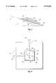
- FIG. 1is a cross-sectional view of a preferred underfill dispensing step for a semiconductor device, a bumped flip-chip, and an inclined substrate in accordance with the present invention
- FIG. 2is a cross-sectional view of a another preferred underfill dispensing method, which illustrates the placement of a suitable barrier, a fence, located adjacent the substrate;
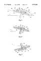
- FIG. 3is a side view illustrating the placement of the semiconductor device, bumped flip-chip, and substrate of FIG. 1 on top of a support member having a vibrator attached thereto;
- FIG. 4is a top view of a semiconductor device, bumped flip-chip, and an inclined substrate illustrating the use of two suitable barriers, fences, to perform the underfill step;
- FIG. 5is a cross-sectional view of another embodiment of the present invention, illustrating a backfill method of underfilling the gap formed between a semiconductor device, bumped flip-chip, and a substrate.
- FIG. 6is a cross-sectional view of another embodiment of the present invention, illustrating a backfill method of underfilling the gap formed between a semiconductor device, a bumped flip-chip, and a substrate without the use of dams.
- FIG. 7is a cross-sectional view of another embodiment of the present invention, illustrating a backfill method of underfilling the gap formed between a semiconductor device, a bumped flip-chip, and a substrate wherein the substrate is inverted during the underfilling process.
- a substrate or chip carrier 10is shown for connecting a semiconductor device or flip-chip 12 by conventional direct chip bonding techniques.
- Substrate 10is typically made of ceramic, silicone, glass, and combinations thereof.
- Substrate 10is preferably comprised of a printed circuit board (PCB) or other carrier, which is used in flip-chip technology, such as an FR4 PCB.
- PCBprinted circuit board
- Substrate 10has a front end 14, a rear end 16, and a top surface 18. The top surface 18 having contact pads thereon.
- Flip-chip 12has a front sidewall 30, a rear sidewall 32, and an active surface 20.
- the active surface 20comprises integrated circuitry and a plurality of contact pads 22.
- the contact pads 22have bumps 24 thereon, which provide both electrical and mechanical connection to substrate 10.
- An electrical assemblyis produced by placing and securing the flip-chip 12 on the top surface 18 of substrate 10 having active circuitry thereon. Specifically, the bumps 24 are aligned with the contact pads of the active circuitry located on top surface 18 of substrate 10. The flip-chip 12 is then electrically and mechanically connected to the substrate 10 by curing or reflowing the bumps 24, depending upon type of material comprising the bumps 24. Alternatively, the bumps 24 may be formed on the substrate 10 prior to attachment of the flip-chip. In other words, either surface may bear the bumps thereon. Although bumps 24 are typically formed with solder, it is understood that any other materials known in the art (e.g. gold, indium, tin lead, silver or alloys thereof) that reflow to make electrical interconnects to substrate 10 can also be used. Additionally, the bumps 24 may be formed of conductive polymeric and epoxy materials and may include various metals being plated thereon.
- a space or gap 26is formed between the active surface 20 of flip-chip 12 and the top surface 18 of substrate 10.
- the size of the gap 26is controlled by the size of the reflowed solder bumps and typically varies from approximately 3 to about 10 mils.
- an underfill material 28is applied to fill the gap 26 between the flip-chip 12 and the substrate 10.
- the purpose of the underfill material 28is to environmentally seal the active surface 20 of the flip-chip 12 and the bumps 24, help provide an additional mechanical bond between the flip-chip 12 and the substrate 10 to help prevent distribute stress on the flip-chip 12 and bumps 24 and to help transfer heat from the flip-chip 12.
- the underfill materialis typically a polymeric material, such as an epoxy or an acrylic resin and may contain inert filler material therein.
- the underfill material 28typically has a thermal coefficient of expansion that approximates that of the flip-chip 12 and/or the substrate 10 to help minimize stress placed on either the flip-chip 12 or the substrate 10 during the operation of the flip-chip caused by the heating of the underfill material 28.
- the viscosity of the underfill material 28is controlled taking into account the flow characteristics of the underfill material, the material characteristics of the substrate 10, the material characteristics of the flip-chip 12, and the size of the gap.
- the underfill processis started by elevating or inclining the front end 14 of the substrate 10 in order to position the substrate 10 on an inclined plane 2 with respect to a horizontal plane 1.
- the angle of elevation or inclination of the inclined plane 2 and the attendant substrate 10 and flip-chip 12is dependent on the viscosity or the rate of dispensing of the underfill material 28.
- the viscosity of the underfill material 28should be adjusted to allow facile flow of the underfill material 28 but should be left low enough to readily prevent the flow of the underfill material 28 beyond the perimeter of the flip-chip 12.
- the substrate 10may be inclined by placing the substrate 10 on a support member 44, such as a tilted table or conveyor belt, as is shown in FIG. 3 and further described below. Alternately, the substrate 10 may be inclined by placing the substrate 10 below a support member or horizontal plume 1 as described hereinbelow.
- Underfillingis accomplished by applying the underfill material 28 under the front sidewall 30 of flip-chip 12 and allowing it to flow between the flip-chip 12 and the substrate 10 and around the bumps 24.
- the underfill material 28is applied with an underfill dispenser 34, such as syringe having a suitable nozzle thereon or any other dispensing means known in the art.
- a gravitational forcealso acts on the underfill material causing the underfill material 28 to readily flow from front sidewall 30 toward rear sidewall 32. Due to the additional action of the gravitational force to that of the injection pressure and capillary action, air pockets, bubbles, and voids found within the underfill material 28 are displaced by the denser underfill material 28 as it flows toward the rear sidewall 32 of flip-chip 12.
- the ability to displace and the speed of displacement of the voidsis dependent on the inclined angle of the substrate 10 having flip-chip 12 thereon, the viscosity of the underfill material 28, the injection rate of the underfill material 28, and the uniformity of the injection of the underfill material 28 into the gap between the substrate 10 and the flip-chip 12 to form a substantially uniform flow front of underfill into and through the gap.
- the process of underfilling the gapmay be repeated by inclining the substrate 10 in the opposite direction and subsequently dispensing another amount of underfill material 28 from an opposing side of the flip-chip 12 into the gap to improve the uniformity of the underfill material 28 filling the gap.
- the materialAfter application of the underfill material 28, the material is cured either by heat, ultraviolet light, radiation, or other suitable means in order to form a solid mass.
- a dam or barrier 40is used on the top surface 18 of the substrate 10 to help contain the flow of the underfill from the gap at the rear sidewall 32 of the flip-chip 12.
- Conventional molding equipment and techniquese.g. pour molding, injection molding, adhesive bonding,etc.
- the dam 40is typically formed from any suitable epoxy resin material compatible with the substrate 10.
- the dam 40extends upwards from and is substantially perpendicular to the top surface 18 of the substrate 10. As shown, the dam 40 may be seen to lay substantially parallel and slightly aft the rear sidewall 32 of the flip-chip 12.
- the dam 40limits the expansion or gravitational flow of the underfill material 28 beyond the position of the dam 40.
- the underfill material 28coats and spreads out onto the surfaces of the flip-chip 12 and substrate 10.
- the dam 40prevents the spread of underfill material 28 beyond the rear sidewall 32 of the flip-chip 12 by means of surface tension.
- dam 40permits use of lower viscosity underfill materials, if so desired, during the underfill procedure.
- the underfill materialmay be easily controlled and a wider range of viscosities may be used by controlling the depth of the dam 40 and by controlling the width between the rear sidewall 32 of the flip-chip 12 and the dam 40.
- Use of the dam 40also permits tilting the substrate 10 at a greater angle of elevation with respect to the horizontal plane 1 in order to accelerate the underfill process or to permit the use of higher viscosity underfill materials should such a need arise.
- a dam 40may be used on all three sides of the flip-chip 12 located on the substrate 10 except the side of the flip-chip 12 from which the underfill material 28 is being dispensed.
- FIG. 3a side view of a flip-chip 12 and substrate 10, interconnected via bumps 24, of a third embodiment of the invention is shown.
- the substrate 10is inclined with respect to a horizontal plane 1 by placing the substrate 10 onto a support member 44.
- Support member 44can be a tilt table, a tilted conveyor belt, or any other means of support suitable for holding the substrate 10 of the present invention.
- support member 44can be positioned and locked at various angles and can also be elevated or lowered from front to back as well as side to side.
- the vibrator 48facilitates and hastens the displacement of air pockets and voids by the underfill material 28 during the previously described underfill process.
- the action of the vibrator 48also permits the use of higher viscosity underfill materials and/or permits underfilling with the support member 44 positioned at a gradual slope.
- FIG. 4a top view of an interconnected solder-bumped 24 flip-chip 12 and substrate 10 of a fourth embodiment of the present invention is shown similar to that of the second embodiment as shown in FIG. 2.
- this particular embodimentillustrates the use of two dams 40 and 40', which are oriented transversely with respect to one another.
- the two dams 40 and 40'lie in substantially parallel orientation with respect to two mutually perpendicular and abutting sidewalls 50 and 52 of the flip-chip 12.
- the method of this embodimentpermits underfilling along two sidewalls 54 and 56 simultaneously. Dams 40 and 40' prevent the spread and overflow of underfill material 28 beyond sidewalls 50 and 52 of the flip-chip 12.
- the underfill materialmay be easily controlled and a wider range of viscosities may be used by controlling the depth of the fences 40 and 40', by controlling the width between the sidewalls 50 and 52 of the flip-chip 12 and the fences 40 and 40', and by controlling the distance between the corners 60 and 60' of the dams 40 and 40'.
- An alternative methodcomprises tilting the substrate 10 so as to elevate sidewall 54 and applying the underfill material 28 under sidewall 54 via the underfill dispenser 34'.
- the substrate 10is then tilted so as to elevate sidewall 56 and the underfill material 28 is dispensed along sidewall 56 via underfill dispenser 34.
- This alternating underfill techniquecan be repeated until the underfill material 28 is free of air pockets and voids.
- FIG. 5a cross-sectional view of an interconnected solder-bumped 24 flip-chip 12 and substrate 10 of a fifth embodiment of the present invention is shown midway through the underfill process.
- the substrate 10has a suitable shaped opening 60 situated near the center of the substrate 10 through which underfill material 28 can be applied via the underfill dispenser 34.
- dams 40 and 40' located on each side of the flip-chip 12are molded or suitably attached to top surface 18 of the substrate 10 as described hereinbefore being positioned to lay slightly beyond first and second sidewalls, rear sidewall 32, and front sidewall 30, respectively. It should also be understood that other dams 40' (not shown) are located on the first and second lateral sidewalls of the flip-chip 12 to confine the underfill.
- FIG. 6a cross-sectional view of an interconnected solder-bumped 24 flip-chip 12 and substrate 10 of a sixth embodiment of the present invention is shown midway through the underfill process.
- the substrate 10has a suitable shaped opening 60 situated near the center of the substrate 10 through which underfill material 28 can be applied via the underfill dispenser 34. In this instance, there is no dam used to confine the underfill material 28.
- the substrate 10 having flip-chip 12 located thereonmay be tilted in each direction to enhance the flow of the underfill material 28 in the gap 26 between the substrate 10 and the flip-chip 12 during the underfilling process.
- FIG. 7a cross-sectional view of an interconnected solder-bumped 24 flip-chip 12 and substrate 10 of a seventh embodiment of the present invention is shown midway through the underfill process.
- the substrate 10has a suitable shaped opening 60 situated near the center of the substrate 10 through which underfill material 28 can be applied via the underfill dispenser 34.
- dams 40 and 40' located on each side of the flip-chip 12are molded or suitably attached to top surface 18 of the substrate 10 as described hereinbefore being positioned to lay slightly beyond first and second sidewalls, rear sidewall 32, and front said wall 30, respectively.
- dams 40'are located on the first and second lateral sidewalls of the flip-chip 12 to confine the underfill.
- the substrate 10 having flip-chip 12 located thereonis inverted during the underfill process so that the underfill material 28 is dispensed through the opening 60 into the gap 28 between the substrate 10 and flip-chip 12.
- the substrate 10is located at an angle with respect to horizontal plane 1 although located therebelow and inclined with respect thereto.
- the present methodis initiated by elevating or inclining front end 14 of the substrate 10.
- the underfill material 28is added, in this case by means of an opening 60 through the substrate 10, the underfill material 28 flows towards the fence 40 and fills the lowered portion of the gap 26 between the flip-chip 12 and the substrate 10.
- the front end 14 of the substrate 10is then lowered and the rear end 32 of the substrate 10 is elevated.
- the backfill methodis then repeated with the underfill material 28 now flowing towards the dam 40' to complete the filling of the gap 26 between the flip-chip 12 and the substrate 10.
- the underfill material 28is then cured, as previously described. Alternately, the underfill material 28 may be cured after the partial filling of the gap between the substrate 10 and flip-chip 12, the remainder of the gap filled and subsequently cured.
Landscapes
- Engineering & Computer Science (AREA)
- Computer Hardware Design (AREA)
- Microelectronics & Electronic Packaging (AREA)
- Power Engineering (AREA)
- Physics & Mathematics (AREA)
- Condensed Matter Physics & Semiconductors (AREA)
- General Physics & Mathematics (AREA)
- Manufacturing & Machinery (AREA)
- Encapsulation Of And Coatings For Semiconductor Or Solid State Devices (AREA)
- Wire Bonding (AREA)
Abstract
Description
Claims (13)
Priority Applications (5)
| Application Number | Priority Date | Filing Date | Title |
|---|---|---|---|
| US08/910,299US5973404A (en) | 1996-03-07 | 1997-08-11 | Underfill of bumped or raised die using a barrier adjacent to the sidewall of semiconductor device |
| US09/304,502US6194243B1 (en) | 1996-03-07 | 1999-05-03 | Method of production an underfill of a bumped or raised die using a barrier adjacent to the sidewall of a semiconductor device |
| US09/619,595US6376918B1 (en) | 1996-03-07 | 2000-07-19 | Underfill of a bumped or raised die utilizing a barrier adjacent to the side wall of slip chip |
| US09/991,010US6455933B1 (en) | 1996-03-07 | 2001-11-16 | Underfill of a bumped or raised die utilizing a barrier adjacent to the side wall of flip chip |
| US10/200,853US6815817B2 (en) | 1996-03-07 | 2002-07-22 | Underfill of a bumped or raised die utilizing barrier adjacent to the side wall of a flip-chip |
Applications Claiming Priority (2)
| Application Number | Priority Date | Filing Date | Title |
|---|---|---|---|
| US08/612,125US5766982A (en) | 1996-03-07 | 1996-03-07 | Method and apparatus for underfill of bumped or raised die |
| US08/910,299US5973404A (en) | 1996-03-07 | 1997-08-11 | Underfill of bumped or raised die using a barrier adjacent to the sidewall of semiconductor device |
Related Parent Applications (1)
| Application Number | Title | Priority Date | Filing Date |
|---|---|---|---|
| US08/612,125DivisionUS5766982A (en) | 1996-03-07 | 1996-03-07 | Method and apparatus for underfill of bumped or raised die |
Related Child Applications (1)
| Application Number | Title | Priority Date | Filing Date |
|---|---|---|---|
| US09/304,502ContinuationUS6194243B1 (en) | 1996-03-07 | 1999-05-03 | Method of production an underfill of a bumped or raised die using a barrier adjacent to the sidewall of a semiconductor device |
Publications (1)
| Publication Number | Publication Date |
|---|---|
| US5973404Atrue US5973404A (en) | 1999-10-26 |
Family
ID=24451838
Family Applications (6)
| Application Number | Title | Priority Date | Filing Date |
|---|---|---|---|
| US08/612,125Expired - LifetimeUS5766982A (en) | 1996-03-07 | 1996-03-07 | Method and apparatus for underfill of bumped or raised die |
| US08/910,299Expired - LifetimeUS5973404A (en) | 1996-03-07 | 1997-08-11 | Underfill of bumped or raised die using a barrier adjacent to the sidewall of semiconductor device |
| US09/304,502Expired - LifetimeUS6194243B1 (en) | 1996-03-07 | 1999-05-03 | Method of production an underfill of a bumped or raised die using a barrier adjacent to the sidewall of a semiconductor device |
| US09/619,595Expired - Fee RelatedUS6376918B1 (en) | 1996-03-07 | 2000-07-19 | Underfill of a bumped or raised die utilizing a barrier adjacent to the side wall of slip chip |
| US09/991,010Expired - LifetimeUS6455933B1 (en) | 1996-03-07 | 2001-11-16 | Underfill of a bumped or raised die utilizing a barrier adjacent to the side wall of flip chip |
| US10/200,853Expired - Fee RelatedUS6815817B2 (en) | 1996-03-07 | 2002-07-22 | Underfill of a bumped or raised die utilizing barrier adjacent to the side wall of a flip-chip |
Family Applications Before (1)
| Application Number | Title | Priority Date | Filing Date |
|---|---|---|---|
| US08/612,125Expired - LifetimeUS5766982A (en) | 1996-03-07 | 1996-03-07 | Method and apparatus for underfill of bumped or raised die |
Family Applications After (4)
| Application Number | Title | Priority Date | Filing Date |
|---|---|---|---|
| US09/304,502Expired - LifetimeUS6194243B1 (en) | 1996-03-07 | 1999-05-03 | Method of production an underfill of a bumped or raised die using a barrier adjacent to the sidewall of a semiconductor device |
| US09/619,595Expired - Fee RelatedUS6376918B1 (en) | 1996-03-07 | 2000-07-19 | Underfill of a bumped or raised die utilizing a barrier adjacent to the side wall of slip chip |
| US09/991,010Expired - LifetimeUS6455933B1 (en) | 1996-03-07 | 2001-11-16 | Underfill of a bumped or raised die utilizing a barrier adjacent to the side wall of flip chip |
| US10/200,853Expired - Fee RelatedUS6815817B2 (en) | 1996-03-07 | 2002-07-22 | Underfill of a bumped or raised die utilizing barrier adjacent to the side wall of a flip-chip |
Country Status (1)
| Country | Link |
|---|---|
| US (6) | US5766982A (en) |
Cited By (22)
| Publication number | Priority date | Publication date | Assignee | Title |
|---|---|---|---|---|
| US6169325B1 (en)* | 1997-12-17 | 2001-01-02 | Hitachi, Ltd. | Semiconductor device |
| US6194243B1 (en)* | 1996-03-07 | 2001-02-27 | Micron Technology, Inc. | Method of production an underfill of a bumped or raised die using a barrier adjacent to the sidewall of a semiconductor device |
| US6214635B1 (en) | 1996-03-07 | 2001-04-10 | Micron Technology, Inc. | Method and apparatus for underfill of bumped or raised die |
| US6229711B1 (en)* | 1998-08-31 | 2001-05-08 | Shinko Electric Industries Co., Ltd. | Flip-chip mount board and flip-chip mount structure with improved mounting reliability |
| US6291895B1 (en)* | 1998-02-25 | 2001-09-18 | Fujitsu Limited | Method of fabricating semiconductor having through hole |
| US6320754B1 (en)* | 1999-08-06 | 2001-11-20 | Agilent Technologies, Inc. | Apparatus for the reduction of interfacial stress caused by differential thermal expansion in an integrated circuit package |
| US20020060368A1 (en)* | 2000-04-06 | 2002-05-23 | Tongbi Jiang | Underfile process |
| US6400033B1 (en) | 2000-06-01 | 2002-06-04 | Amkor Technology, Inc. | Reinforcing solder connections of electronic devices |
| US6424541B1 (en)* | 1999-04-21 | 2002-07-23 | Conexant Systems, Inc | Electronic device attachment methods and apparatus for forming an assembly |
| US6582990B2 (en)* | 2001-08-24 | 2003-06-24 | International Rectifier Corporation | Wafer level underfill and interconnect process |
| US20030164543A1 (en)* | 2002-03-04 | 2003-09-04 | Teck Kheng Lee | Interposer configured to reduce the profiles of semiconductor device assemblies and packages including the same and methods |
| US20030164548A1 (en)* | 2002-03-04 | 2003-09-04 | Lee Teck Kheng | Flip chip packaging using recessed interposer terminals |
| US6756251B2 (en) | 2001-08-21 | 2004-06-29 | Micron Technology, Inc. | Method of manufacturing microelectronic devices, including methods of underfilling microelectronic components through an underfill aperture |
| US20040159957A1 (en)* | 2002-03-04 | 2004-08-19 | Lee Teck Kheng | Interposer substrate and wafer scale interposer substrate member for use with flip-chip configured semiconductor dice |
| US20040184226A1 (en)* | 2003-03-18 | 2004-09-23 | Hall Frank L. | Bare die semiconductor dice underfilled and encapsulated with a single dielectric material and method for manufacturing the same |
| US20040219713A1 (en)* | 2002-01-09 | 2004-11-04 | Micron Technology, Inc. | Elimination of RDL using tape base flip chip on flex for die stacking |
| US7087460B2 (en) | 2002-03-04 | 2006-08-08 | Micron Technology, Inc. | Methods for assembly and packaging of flip chip configured dice with interposer |
| US7112520B2 (en) | 2002-03-04 | 2006-09-26 | Micron Technology, Inc. | Semiconductor die packages with recessed interconnecting structures and methods for assembling the same |
| US7115986B2 (en) | 2001-05-02 | 2006-10-03 | Micron Technology, Inc. | Flexible ball grid array chip scale packages |
| US20070269930A1 (en)* | 2006-05-19 | 2007-11-22 | Texas Instruments Incorporated | Methodology to control underfill fillet size, flow-out and bleed in flip chips (FC), chip scale packages (CSP) and ball grid arrays (BGA) |
| US7320933B2 (en) | 2002-08-20 | 2008-01-22 | Micron Technology, Inc. | Double bumping of flexible substrate for first and second level interconnects |
| US7915718B2 (en) | 2002-03-04 | 2011-03-29 | Micron Technology, Inc. | Apparatus for flip-chip packaging providing testing capability |
Families Citing this family (82)
| Publication number | Priority date | Publication date | Assignee | Title |
|---|---|---|---|---|
| US5784260A (en)* | 1996-05-29 | 1998-07-21 | International Business Machines Corporation | Structure for constraining the flow of encapsulant applied to an I/C chip on a substrate |
| WO1998027411A1 (en)* | 1996-12-17 | 1998-06-25 | Laboratorium Für Physikalische Elektronik Institut Für Quantenelektronik | Method for applying a microsystem or a converter on a substrate, and device manufactured accordingly |
| US6001672A (en) | 1997-02-25 | 1999-12-14 | Micron Technology, Inc. | Method for transfer molding encapsulation of a semiconductor die with attached heat sink |
| JPH10270496A (en)* | 1997-03-27 | 1998-10-09 | Hitachi Ltd | Electronic device, information processing device, semiconductor device, and semiconductor chip mounting method |
| EP2015359B1 (en)* | 1997-05-09 | 2015-12-23 | Citizen Holdings Co., Ltd. | Process for manufacturing a semiconductor package and circuit board substrate |
| US6057178A (en) | 1997-09-26 | 2000-05-02 | Siemens Aktiengesellschaft | Method of padding an electronic component, mounted on a flat substrate, with a liquid filler |
| JP3876953B2 (en) | 1998-03-27 | 2007-02-07 | セイコーエプソン株式会社 | Semiconductor device and manufacturing method thereof, circuit board, and electronic apparatus |
| US6194782B1 (en)* | 1998-06-24 | 2001-02-27 | Nortel Networks Limited | Mechanically-stabilized area-array device package |
| JP2000022039A (en)* | 1998-07-06 | 2000-01-21 | Shinko Electric Ind Co Ltd | Semiconductor device and its manufacture |
| US6130823A (en)* | 1999-02-01 | 2000-10-10 | Raytheon E-Systems, Inc. | Stackable ball grid array module and method |
| US6220503B1 (en) | 1999-02-02 | 2001-04-24 | International Business Machines Corporation | Rework and underfill nozzle for electronic components |
| DE19908474C2 (en)* | 1999-02-26 | 2001-02-15 | Siemens Ag | Method for mounting a semiconductor chip on a base layer |
| US6528345B1 (en) | 1999-03-03 | 2003-03-04 | Intel Corporation | Process line for underfilling a controlled collapse |
| US6238948B1 (en)* | 1999-03-03 | 2001-05-29 | Intel Corporation | Controlled collapse chip connection (C4) integrated circuit package that has a fillet which seals an underfill material |
| US20020014688A1 (en) | 1999-03-03 | 2002-02-07 | Suresh Ramalingam | Controlled collapse chip connection (c4) integrated circuit package which has two dissimilar underfill materials |
| US6331446B1 (en) | 1999-03-03 | 2001-12-18 | Intel Corporation | Process for underfilling a controlled collapse chip connection (C4) integrated circuit package with an underfill material that is heated to a partial gel state |
| JP2000260792A (en)* | 1999-03-10 | 2000-09-22 | Toshiba Corp | Semiconductor device |
| US6259155B1 (en) | 1999-04-12 | 2001-07-10 | International Business Machines Corporation | Polymer enhanced column grid array |
| US6048656A (en)* | 1999-05-11 | 2000-04-11 | Micron Technology, Inc. | Void-free underfill of surface mounted chips |
| US6490166B1 (en) | 1999-06-11 | 2002-12-03 | Intel Corporation | Integrated circuit package having a substrate vent hole |
| US6700209B1 (en) | 1999-12-29 | 2004-03-02 | Intel Corporation | Partial underfill for flip-chip electronic packages |
| US6444499B1 (en) | 2000-03-30 | 2002-09-03 | Amkor Technology, Inc. | Method for fabricating a snapable multi-package array substrate, snapable multi-package array and snapable packaged electronic components |
| US6838319B1 (en)* | 2000-08-31 | 2005-01-04 | Micron Technology, Inc. | Transfer molding and underfilling method and apparatus including orienting the active surface of a semiconductor substrate substantially vertically |
| US7007835B2 (en)* | 2001-05-21 | 2006-03-07 | Jds Uniphase Corporation | Solder bonding technique for assembling a tilted chip or substrate |
| US7220615B2 (en)* | 2001-06-11 | 2007-05-22 | Micron Technology, Inc. | Alternative method used to package multimedia card by transfer molding |
| US6444501B1 (en)* | 2001-06-12 | 2002-09-03 | Micron Technology, Inc. | Two stage transfer molding method to encapsulate MMC module |
| TW529215B (en)* | 2001-08-24 | 2003-04-21 | Inpaq Technology Co Ltd | IC carrying substrate with an over voltage protection function |
| KR100446290B1 (en)* | 2001-11-03 | 2004-09-01 | 삼성전자주식회사 | Semiconductor package having dam and fabricating method the same |
| US6762509B2 (en)* | 2001-12-11 | 2004-07-13 | Celerity Research Pte. Ltd. | Flip-chip packaging method that treats an interconnect substrate to control stress created at edges of fill material |
| US20030113952A1 (en)* | 2001-12-19 | 2003-06-19 | Mahesh Sambasivam | Underfill materials dispensed in a flip chip package by way of a through hole |
| US8148803B2 (en)* | 2002-02-15 | 2012-04-03 | Micron Technology, Inc. | Molded stiffener for thin substrates |
| US6765469B2 (en) | 2002-02-21 | 2004-07-20 | Eni Technology, Inc. | Printed circuit board transformer |
| US6861278B2 (en)* | 2002-04-11 | 2005-03-01 | Nordson Corporation | Method and apparatus for underfilling semiconductor devices |
| TWI286832B (en)* | 2002-11-05 | 2007-09-11 | Advanced Semiconductor Eng | Thermal enhance semiconductor package |
| JP3918098B2 (en)* | 2002-11-14 | 2007-05-23 | 株式会社村田製作所 | Circuit module manufacturing method |
| US20040129453A1 (en)* | 2003-01-07 | 2004-07-08 | Boggs David W. | Electronic substrate with direct inner layer component interconnection |
| US20040214370A1 (en)* | 2003-01-28 | 2004-10-28 | Nordson Corporation | Method for efficient capillary underfill |
| FR2856517B1 (en)* | 2003-06-17 | 2005-09-23 | St Microelectronics Sa | METHOD FOR MANUFACTURING SEMICONDUCTOR COMPONENT AND SEMICONDUCTOR COMPONENT |
| US7141884B2 (en)* | 2003-07-03 | 2006-11-28 | Matsushita Electric Industrial Co., Ltd. | Module with a built-in semiconductor and method for producing the same |
| GB0319764D0 (en)* | 2003-08-22 | 2003-09-24 | Trikon Technologies Ltd | A method of forming a substanially closed void |
| US7124931B2 (en)* | 2003-11-18 | 2006-10-24 | Intel Corporation | Via heat sink material |
| TWI231578B (en)* | 2003-12-01 | 2005-04-21 | Advanced Semiconductor Eng | Anti-warpage package and method for making the same |
| US6993835B2 (en)* | 2003-12-04 | 2006-02-07 | Irvine Sensors Corp. | Method for electrical interconnection of angularly disposed conductive patterns |
| US7190706B2 (en)* | 2003-12-10 | 2007-03-13 | Avago Technologies Fiber Ip (Singapore) Ptd. Ltd. | Soft metal heat transfer for transceivers |
| US7075016B2 (en)* | 2004-02-18 | 2006-07-11 | Taiwan Semiconductor Manufacturing Co., Ltd. | Underfilling efficiency by modifying the substrate design of flip chips |
| US8067837B2 (en) | 2004-09-20 | 2011-11-29 | Megica Corporation | Metallization structure over passivation layer for IC chip |
| JP4385329B2 (en)* | 2004-10-08 | 2009-12-16 | Okiセミコンダクタ株式会社 | Manufacturing method of semiconductor device |
| US20060099736A1 (en)* | 2004-11-09 | 2006-05-11 | Nagar Mohan R | Flip chip underfilling |
| US20060234427A1 (en)* | 2005-04-19 | 2006-10-19 | Odegard Charles A | Underfill dispense at substrate aperture |
| US20060270106A1 (en)* | 2005-05-31 | 2006-11-30 | Tz-Cheng Chiu | System and method for polymer encapsulated solder lid attach |
| DE112005003634T5 (en)* | 2005-08-04 | 2008-06-12 | Infineon Technologies Ag | An integrated circuit device and method for forming an integrated circuit device |
| US20070043510A1 (en)* | 2005-08-19 | 2007-02-22 | Beckman Coulter, Inc. | Assay system |
| US7585702B1 (en) | 2005-11-08 | 2009-09-08 | Altera Corporation | Structure and assembly procedure for low stress thin die flip chip packages designed for low-K Si and thin core substrate |
| US20070166875A1 (en)* | 2005-12-29 | 2007-07-19 | Intel Corporation | Method of forming a microelectronic package and microelectronic package formed according to the method |
| US7485502B2 (en)* | 2006-01-31 | 2009-02-03 | Stats Chippac Ltd. | Integrated circuit underfill package system |
| US20070228111A1 (en)* | 2006-03-29 | 2007-10-04 | Vasudevanpillai Ganesh V | Microelectronic package and method of forming same |
| US7592702B2 (en)* | 2006-07-31 | 2009-09-22 | Intel Corporation | Via heat sink material |
| US7927923B2 (en)* | 2006-09-25 | 2011-04-19 | Micron Technology, Inc. | Method and apparatus for directing molding compound flow and resulting semiconductor device packages |
| US20080160670A1 (en)* | 2006-12-27 | 2008-07-03 | Atmel Corporation | Physical alignment features on integrated circuit devices for accurate die-in-substrate embedding |
| JP5050573B2 (en)* | 2007-03-05 | 2012-10-17 | 富士通株式会社 | Manufacturing method of electronic device |
| US7883937B1 (en)* | 2007-04-30 | 2011-02-08 | Altera Corporation | Electronic package and method of forming the same |
| JP4973463B2 (en)* | 2007-11-16 | 2012-07-11 | トヨタ自動車株式会社 | Semiconductor device |
| US8009442B2 (en)* | 2007-12-28 | 2011-08-30 | Intel Corporation | Directing the flow of underfill materials using magnetic particles |
| JP2009212501A (en)* | 2008-02-08 | 2009-09-17 | Seiko Instruments Inc | Light emitting device and method of manufacturing the same |
| JP4693852B2 (en)* | 2008-02-22 | 2011-06-01 | パナソニック株式会社 | Semiconductor device and manufacturing method of semiconductor device |
| US8193036B2 (en)* | 2010-09-14 | 2012-06-05 | Stats Chippac, Ltd. | Semiconductor device and method of forming mold underfill using dispensing needle having same width as semiconductor die |
| US8796075B2 (en) | 2011-01-11 | 2014-08-05 | Nordson Corporation | Methods for vacuum assisted underfilling |
| US10269747B2 (en)* | 2012-10-25 | 2019-04-23 | Taiwan Semiconductor Manufacturing Company | Semiconductor devices, methods of manufacture thereof, and packaged semiconductor devices |
| US9627229B2 (en)* | 2013-06-27 | 2017-04-18 | STATS ChipPAC Pte. Ltd. | Semiconductor device and method of forming trench and disposing semiconductor die over substrate to control outward flow of underfill material |
| US9508701B2 (en) | 2013-09-27 | 2016-11-29 | Freescale Semiconductor, Inc. | 3D device packaging using through-substrate pillars |
| US9508702B2 (en) | 2013-09-27 | 2016-11-29 | Freescale Semiconductor, Inc. | 3D device packaging using through-substrate posts |
| US9515006B2 (en) | 2013-09-27 | 2016-12-06 | Freescale Semiconductor, Inc. | 3D device packaging using through-substrate posts |
| US9373559B2 (en) | 2014-03-05 | 2016-06-21 | International Business Machines Corporation | Low-stress dual underfill packaging |
| US9425179B2 (en)* | 2014-08-29 | 2016-08-23 | Taiwan Semiconductor Manufacturing Company, Ltd. | Chip packages and methods of manufacture thereof |
| US9721812B2 (en)* | 2015-11-20 | 2017-08-01 | International Business Machines Corporation | Optical device with precoated underfill |
| US10687447B2 (en)* | 2016-10-14 | 2020-06-16 | Laird Technologies, Inc. | Methods of applying thermal interface materials to board level shields |
| DE102017204842A1 (en) | 2017-03-22 | 2018-09-27 | Robert Bosch Gmbh | Contact configuration |
| US20190364671A1 (en)* | 2017-03-29 | 2019-11-28 | Sharp Kabushiki Kaisha | Mounting method, mounting device, and production device |
| US10586716B2 (en) | 2017-06-09 | 2020-03-10 | Advanced Semiconductor Engineering, Inc. | Semiconductor device package |
| US11282717B2 (en)* | 2018-03-30 | 2022-03-22 | Intel Corporation | Micro-electronic package with substrate protrusion to facilitate dispense of underfill between a narrow die-to-die gap |
| US11152226B2 (en)* | 2019-10-15 | 2021-10-19 | International Business Machines Corporation | Structure with controlled capillary coverage |
| US12362316B2 (en)* | 2022-02-11 | 2025-07-15 | Advanced Semiconductor Engineering, Inc. | Electronic structure having a protrusion structure disposed in a gap between a circuit pattern structure and a packaging structure |
Citations (21)
| Publication number | Priority date | Publication date | Assignee | Title |
|---|---|---|---|---|
| JPS5795651A (en)* | 1980-12-04 | 1982-06-14 | Nec Corp | Semiconductor device |
| US5203076A (en)* | 1991-12-23 | 1993-04-20 | Motorola, Inc. | Vacuum infiltration of underfill material for flip-chip devices |
| US5218234A (en)* | 1991-12-23 | 1993-06-08 | Motorola, Inc. | Semiconductor device with controlled spread polymeric underfill |
| US5239447A (en)* | 1991-09-13 | 1993-08-24 | International Business Machines Corporation | Stepped electronic device package |
| US5258648A (en)* | 1991-06-27 | 1993-11-02 | Motorola, Inc. | Composite flip chip semiconductor device with an interposer having test contacts formed along its periphery |
| US5289346A (en)* | 1991-02-26 | 1994-02-22 | Microelectronics And Computer Technology Corporation | Peripheral to area adapter with protective bumper for an integrated circuit chip |
| US5311059A (en)* | 1992-01-24 | 1994-05-10 | Motorola, Inc. | Backplane grounding for flip-chip integrated circuit |
| US5371404A (en)* | 1993-02-04 | 1994-12-06 | Motorola, Inc. | Thermally conductive integrated circuit package with radio frequency shielding |
| US5385869A (en)* | 1993-07-22 | 1995-01-31 | Motorola, Inc. | Semiconductor chip bonded to a substrate and method of making |
| US5403439A (en)* | 1993-12-01 | 1995-04-04 | Texas Instruments Incorporated | Method of producing same-sized particles |
| US5410181A (en)* | 1994-06-20 | 1995-04-25 | Motorola, Inc. | Assembly for mounting an electronic device having an optically erasable surface |
| US5436503A (en)* | 1992-11-18 | 1995-07-25 | Matsushita Electronics Corporation | Semiconductor device and method of manufacturing the same |
| US5438219A (en)* | 1993-11-30 | 1995-08-01 | Motorola, Inc. | Double-sided oscillator package and method of coupling components thereto |
| US5439162A (en)* | 1993-06-28 | 1995-08-08 | Motorola, Inc. | Direct chip attachment structure and method |
| US5442240A (en)* | 1994-04-05 | 1995-08-15 | Motorola, Inc. | Method of adhesion to a polyimide surface by formation of covalent bonds |
| US5450283A (en)* | 1992-11-03 | 1995-09-12 | Motorola, Inc. | Thermally enhanced semiconductor device having exposed backside and method for making the same |
| US5468995A (en)* | 1994-07-05 | 1995-11-21 | Motorola, Inc. | Semiconductor device having compliant columnar electrical connections |
| US5498576A (en)* | 1994-07-22 | 1996-03-12 | Texas Instruments Incorporated | Method and apparatus for affixing spheres to a foil matrix |
| US5532187A (en)* | 1993-12-16 | 1996-07-02 | Vdo Kienzle Gmbh | Process for sealing apertures in glass-silicon-glass micromechanical acceleration sensors |
| US5590462A (en)* | 1992-02-15 | 1997-01-07 | Sgs-Thomson Microelectronics S.R.L. | Process for dissipating heat from a semiconductor package |
| US5697148A (en)* | 1995-08-22 | 1997-12-16 | Motorola, Inc. | Flip underfill injection technique |
Family Cites Families (13)
| Publication number | Priority date | Publication date | Assignee | Title |
|---|---|---|---|---|
| JP2830375B2 (en)* | 1990-05-22 | 1998-12-02 | 松下電器産業株式会社 | Semiconductor element mounting method |
| JPH06306717A (en) | 1993-04-16 | 1994-11-01 | Teijin Seiki Co Ltd | Device for supplying bobbin of yarn winder |
| US5677246A (en)* | 1994-11-29 | 1997-10-14 | Kabushiki Kaisha Toshiba | Method of manufacturing semiconductor devices |
| JPH08153738A (en)* | 1994-11-29 | 1996-06-11 | Toshiba Corp | Method for manufacturing semiconductor device |
| JP3272889B2 (en)* | 1994-11-29 | 2002-04-08 | 株式会社東芝 | Method for manufacturing semiconductor device |
| JPH08306717A (en)* | 1995-05-09 | 1996-11-22 | Matsushita Electric Ind Co Ltd | Resin sealing method |
| US5804881A (en)* | 1995-11-27 | 1998-09-08 | Motorola, Inc. | Method and assembly for providing improved underchip encapsulation |
| US5710071A (en)* | 1995-12-04 | 1998-01-20 | Motorola, Inc. | Process for underfilling a flip-chip semiconductor device |
| JP4108773B2 (en)* | 1996-02-22 | 2008-06-25 | 松下電器産業株式会社 | IC chip sealing method |
| US5766982A (en)* | 1996-03-07 | 1998-06-16 | Micron Technology, Inc. | Method and apparatus for underfill of bumped or raised die |
| US6066509A (en)* | 1998-03-12 | 2000-05-23 | Micron Technology, Inc. | Method and apparatus for underfill of bumped or raised die |
| JPH1098077A (en)* | 1996-09-20 | 1998-04-14 | Ricoh Co Ltd | Method for manufacturing semiconductor device |
| JP3333417B2 (en)* | 1997-02-04 | 2002-10-15 | 松下電器産業株式会社 | IC chip sealing method and device |
- 1996
- 1996-03-07USUS08/612,125patent/US5766982A/ennot_activeExpired - Lifetime
- 1997
- 1997-08-11USUS08/910,299patent/US5973404A/ennot_activeExpired - Lifetime
- 1999
- 1999-05-03USUS09/304,502patent/US6194243B1/ennot_activeExpired - Lifetime
- 2000
- 2000-07-19USUS09/619,595patent/US6376918B1/ennot_activeExpired - Fee Related
- 2001
- 2001-11-16USUS09/991,010patent/US6455933B1/ennot_activeExpired - Lifetime
- 2002
- 2002-07-22USUS10/200,853patent/US6815817B2/ennot_activeExpired - Fee Related
Patent Citations (21)
| Publication number | Priority date | Publication date | Assignee | Title |
|---|---|---|---|---|
| JPS5795651A (en)* | 1980-12-04 | 1982-06-14 | Nec Corp | Semiconductor device |
| US5289346A (en)* | 1991-02-26 | 1994-02-22 | Microelectronics And Computer Technology Corporation | Peripheral to area adapter with protective bumper for an integrated circuit chip |
| US5258648A (en)* | 1991-06-27 | 1993-11-02 | Motorola, Inc. | Composite flip chip semiconductor device with an interposer having test contacts formed along its periphery |
| US5239447A (en)* | 1991-09-13 | 1993-08-24 | International Business Machines Corporation | Stepped electronic device package |
| US5203076A (en)* | 1991-12-23 | 1993-04-20 | Motorola, Inc. | Vacuum infiltration of underfill material for flip-chip devices |
| US5218234A (en)* | 1991-12-23 | 1993-06-08 | Motorola, Inc. | Semiconductor device with controlled spread polymeric underfill |
| US5311059A (en)* | 1992-01-24 | 1994-05-10 | Motorola, Inc. | Backplane grounding for flip-chip integrated circuit |
| US5590462A (en)* | 1992-02-15 | 1997-01-07 | Sgs-Thomson Microelectronics S.R.L. | Process for dissipating heat from a semiconductor package |
| US5450283A (en)* | 1992-11-03 | 1995-09-12 | Motorola, Inc. | Thermally enhanced semiconductor device having exposed backside and method for making the same |
| US5436503A (en)* | 1992-11-18 | 1995-07-25 | Matsushita Electronics Corporation | Semiconductor device and method of manufacturing the same |
| US5371404A (en)* | 1993-02-04 | 1994-12-06 | Motorola, Inc. | Thermally conductive integrated circuit package with radio frequency shielding |
| US5439162A (en)* | 1993-06-28 | 1995-08-08 | Motorola, Inc. | Direct chip attachment structure and method |
| US5385869A (en)* | 1993-07-22 | 1995-01-31 | Motorola, Inc. | Semiconductor chip bonded to a substrate and method of making |
| US5438219A (en)* | 1993-11-30 | 1995-08-01 | Motorola, Inc. | Double-sided oscillator package and method of coupling components thereto |
| US5403439A (en)* | 1993-12-01 | 1995-04-04 | Texas Instruments Incorporated | Method of producing same-sized particles |
| US5532187A (en)* | 1993-12-16 | 1996-07-02 | Vdo Kienzle Gmbh | Process for sealing apertures in glass-silicon-glass micromechanical acceleration sensors |
| US5442240A (en)* | 1994-04-05 | 1995-08-15 | Motorola, Inc. | Method of adhesion to a polyimide surface by formation of covalent bonds |
| US5410181A (en)* | 1994-06-20 | 1995-04-25 | Motorola, Inc. | Assembly for mounting an electronic device having an optically erasable surface |
| US5468995A (en)* | 1994-07-05 | 1995-11-21 | Motorola, Inc. | Semiconductor device having compliant columnar electrical connections |
| US5498576A (en)* | 1994-07-22 | 1996-03-12 | Texas Instruments Incorporated | Method and apparatus for affixing spheres to a foil matrix |
| US5697148A (en)* | 1995-08-22 | 1997-12-16 | Motorola, Inc. | Flip underfill injection technique |
Cited By (47)
| Publication number | Priority date | Publication date | Assignee | Title |
|---|---|---|---|---|
| US6455933B1 (en) | 1996-03-07 | 2002-09-24 | Micron Technology, Inc. | Underfill of a bumped or raised die utilizing a barrier adjacent to the side wall of flip chip |
| US6194243B1 (en)* | 1996-03-07 | 2001-02-27 | Micron Technology, Inc. | Method of production an underfill of a bumped or raised die using a barrier adjacent to the sidewall of a semiconductor device |
| US6214635B1 (en) | 1996-03-07 | 2001-04-10 | Micron Technology, Inc. | Method and apparatus for underfill of bumped or raised die |
| US6376918B1 (en) | 1996-03-07 | 2002-04-23 | Micron Technology, Inc. | Underfill of a bumped or raised die utilizing a barrier adjacent to the side wall of slip chip |
| US6815817B2 (en) | 1996-03-07 | 2004-11-09 | Micron Technology, Inc. | Underfill of a bumped or raised die utilizing barrier adjacent to the side wall of a flip-chip |
| US20020185748A1 (en)* | 1996-03-07 | 2002-12-12 | Salman Akram | Underfill of a bumped or raised die utilizing a barrier adjacent to the side wall of flip chip |
| US6169325B1 (en)* | 1997-12-17 | 2001-01-02 | Hitachi, Ltd. | Semiconductor device |
| US6291895B1 (en)* | 1998-02-25 | 2001-09-18 | Fujitsu Limited | Method of fabricating semiconductor having through hole |
| US6229711B1 (en)* | 1998-08-31 | 2001-05-08 | Shinko Electric Industries Co., Ltd. | Flip-chip mount board and flip-chip mount structure with improved mounting reliability |
| US6424541B1 (en)* | 1999-04-21 | 2002-07-23 | Conexant Systems, Inc | Electronic device attachment methods and apparatus for forming an assembly |
| US6320754B1 (en)* | 1999-08-06 | 2001-11-20 | Agilent Technologies, Inc. | Apparatus for the reduction of interfacial stress caused by differential thermal expansion in an integrated circuit package |
| US7547579B1 (en) | 2000-04-06 | 2009-06-16 | Micron Technology, Inc. | Underfill process |
| US20020060368A1 (en)* | 2000-04-06 | 2002-05-23 | Tongbi Jiang | Underfile process |
| US6400033B1 (en) | 2000-06-01 | 2002-06-04 | Amkor Technology, Inc. | Reinforcing solder connections of electronic devices |
| US7115986B2 (en) | 2001-05-02 | 2006-10-03 | Micron Technology, Inc. | Flexible ball grid array chip scale packages |
| US6756251B2 (en) | 2001-08-21 | 2004-06-29 | Micron Technology, Inc. | Method of manufacturing microelectronic devices, including methods of underfilling microelectronic components through an underfill aperture |
| US7087994B2 (en) | 2001-08-21 | 2006-08-08 | Micron Technology, Inc. | Microelectronic devices including underfill apertures |
| US6582990B2 (en)* | 2001-08-24 | 2003-06-24 | International Rectifier Corporation | Wafer level underfill and interconnect process |
| US8441113B2 (en) | 2002-01-09 | 2013-05-14 | Micron Technology, Inc. | Elimination of RDL using tape base flip chip on flex for die stacking |
| US8125065B2 (en) | 2002-01-09 | 2012-02-28 | Micron Technology, Inc. | Elimination of RDL using tape base flip chip on flex for die stacking |
| US7189593B2 (en) | 2002-01-09 | 2007-03-13 | Micron Technology, Inc. | Elimination of RDL using tape base flip chip on flex for die stacking |
| US20040219713A1 (en)* | 2002-01-09 | 2004-11-04 | Micron Technology, Inc. | Elimination of RDL using tape base flip chip on flex for die stacking |
| US7129584B2 (en) | 2002-01-09 | 2006-10-31 | Micron Technology, Inc. | Elimination of RDL using tape base flip chip on flex for die stacking |
| US6975035B2 (en) | 2002-03-04 | 2005-12-13 | Micron Technology, Inc. | Method and apparatus for dielectric filling of flip chip on interposer assembly |
| US20030164548A1 (en)* | 2002-03-04 | 2003-09-04 | Lee Teck Kheng | Flip chip packaging using recessed interposer terminals |
| US20030164543A1 (en)* | 2002-03-04 | 2003-09-04 | Teck Kheng Lee | Interposer configured to reduce the profiles of semiconductor device assemblies and packages including the same and methods |
| US7112520B2 (en) | 2002-03-04 | 2006-09-26 | Micron Technology, Inc. | Semiconductor die packages with recessed interconnecting structures and methods for assembling the same |
| US8269326B2 (en) | 2002-03-04 | 2012-09-18 | Micron Technology, Inc. | Semiconductor device assemblies |
| US7122907B2 (en) | 2002-03-04 | 2006-10-17 | Micron Technology, Inc. | Interposer substrate and wafer scale interposer substrate member for use with flip-chip configured semiconductor dice |
| US7087460B2 (en) | 2002-03-04 | 2006-08-08 | Micron Technology, Inc. | Methods for assembly and packaging of flip chip configured dice with interposer |
| US7145225B2 (en) | 2002-03-04 | 2006-12-05 | Micron Technology, Inc. | Interposer configured to reduce the profiles of semiconductor device assemblies and packages including the same and methods |
| US7161237B2 (en) | 2002-03-04 | 2007-01-09 | Micron Technology, Inc. | Flip chip packaging using recessed interposer terminals |
| US7915718B2 (en) | 2002-03-04 | 2011-03-29 | Micron Technology, Inc. | Apparatus for flip-chip packaging providing testing capability |
| US7230330B2 (en) | 2002-03-04 | 2007-06-12 | Micron Technology, Inc. | Semiconductor die packages with recessed interconnecting structures |
| US20110204499A1 (en)* | 2002-03-04 | 2011-08-25 | Micron Technology, Inc. | Semiconductor device assemblies |
| US7902648B2 (en) | 2002-03-04 | 2011-03-08 | Micron Technology, Inc. | Interposer configured to reduce the profiles of semiconductor device assemblies, packages including the same, and methods |
| US7348215B2 (en) | 2002-03-04 | 2008-03-25 | Micron Technology, Inc. | Methods for assembly and packaging of flip chip configured dice with interposer |
| US7531906B2 (en) | 2002-03-04 | 2009-05-12 | Micron Technology, Inc. | Flip chip packaging using recessed interposer terminals |
| US7534660B2 (en) | 2002-03-04 | 2009-05-19 | Micron Technology, Inc. | Methods for assembly and packaging of flip chip configured dice with interposer |
| US20040159957A1 (en)* | 2002-03-04 | 2004-08-19 | Lee Teck Kheng | Interposer substrate and wafer scale interposer substrate member for use with flip-chip configured semiconductor dice |
| US7569473B2 (en) | 2002-03-04 | 2009-08-04 | Micron Technology, Inc. | Methods of forming semiconductor assemblies |
| US7320933B2 (en) | 2002-08-20 | 2008-01-22 | Micron Technology, Inc. | Double bumping of flexible substrate for first and second level interconnects |
| US20050253241A1 (en)* | 2003-03-18 | 2005-11-17 | Hall Frank L | Semiconductor device assemblies including an encapsulant located over intermediate conductive elements and filling a space between a semiconductor die and a carrier of the assembly |
| US20040184226A1 (en)* | 2003-03-18 | 2004-09-23 | Hall Frank L. | Bare die semiconductor dice underfilled and encapsulated with a single dielectric material and method for manufacturing the same |
| US20050263906A1 (en)* | 2003-03-18 | 2005-12-01 | Hall Frank L | Electronic system including a semiconductor device with at least one semiconductor die, a carrier, and an encapsulant that fills a space between the die and the carrier and covers intermediate conductive elements that connect the die and the carrier |
| US6987058B2 (en)* | 2003-03-18 | 2006-01-17 | Micron Technology, Inc. | Methods for underfilling and encapsulating semiconductor device assemblies with a single dielectric material |
| US20070269930A1 (en)* | 2006-05-19 | 2007-11-22 | Texas Instruments Incorporated | Methodology to control underfill fillet size, flow-out and bleed in flip chips (FC), chip scale packages (CSP) and ball grid arrays (BGA) |
Also Published As
| Publication number | Publication date |
|---|---|
| US6815817B2 (en) | 2004-11-09 |
| US6455933B1 (en) | 2002-09-24 |
| US20020033540A1 (en) | 2002-03-21 |
| US20020185748A1 (en) | 2002-12-12 |
| US5766982A (en) | 1998-06-16 |
| US6376918B1 (en) | 2002-04-23 |
| US6194243B1 (en) | 2001-02-27 |
Similar Documents
| Publication | Publication Date | Title |
|---|---|---|
| US5973404A (en) | Underfill of bumped or raised die using a barrier adjacent to the sidewall of semiconductor device | |
| US6066509A (en) | Method and apparatus for underfill of bumped or raised die | |
| US6048656A (en) | Void-free underfill of surface mounted chips | |
| US7547579B1 (en) | Underfill process | |
| US7550856B2 (en) | Grooved substrates for uniform underfilling solder ball assembled electronic devices | |
| JP3313067B2 (en) | Method and apparatus for injection mold flip chip encapsulation | |
| US8188598B2 (en) | Bump-on-lead flip chip interconnection | |
| US6495083B2 (en) | Method of underfilling an integrated circuit chip | |
| US6232667B1 (en) | Technique for underfilling stacked chips on a cavity MLC module | |
| US20020192861A1 (en) | Method and apparatus for filling a gap between spaced layers of a semiconductor | |
| WO2000070678A1 (en) | Chip package with molded underfill | |
| US6838758B1 (en) | Package and method for making an underfilled integrated circuit | |
| JPH1098077A (en) | Method for manufacturing semiconductor device | |
| JP3475575B2 (en) | Semiconductor chip sealing method and sealing structure | |
| TW488041B (en) | An underfilling method of bonding gap between flip-chip and circuit board | |
| KR20020035477A (en) | Chip package with molded underfill | |
| HK1069677A (en) | Method for efficient capillary underfill |
Legal Events
| Date | Code | Title | Description |
|---|---|---|---|
| STCF | Information on status: patent grant | Free format text:PATENTED CASE | |
| CC | Certificate of correction | ||
| FPAY | Fee payment | Year of fee payment:4 | |
| FPAY | Fee payment | Year of fee payment:8 | |
| FPAY | Fee payment | Year of fee payment:12 | |
| AS | Assignment | Owner name:U.S. BANK NATIONAL ASSOCIATION, AS COLLATERAL AGENT, CALIFORNIA Free format text:SECURITY INTEREST;ASSIGNOR:MICRON TECHNOLOGY, INC.;REEL/FRAME:038669/0001 Effective date:20160426 Owner name:U.S. BANK NATIONAL ASSOCIATION, AS COLLATERAL AGEN Free format text:SECURITY INTEREST;ASSIGNOR:MICRON TECHNOLOGY, INC.;REEL/FRAME:038669/0001 Effective date:20160426 | |
| AS | Assignment | Owner name:MORGAN STANLEY SENIOR FUNDING, INC., AS COLLATERAL AGENT, MARYLAND Free format text:PATENT SECURITY AGREEMENT;ASSIGNOR:MICRON TECHNOLOGY, INC.;REEL/FRAME:038954/0001 Effective date:20160426 Owner name:MORGAN STANLEY SENIOR FUNDING, INC., AS COLLATERAL Free format text:PATENT SECURITY AGREEMENT;ASSIGNOR:MICRON TECHNOLOGY, INC.;REEL/FRAME:038954/0001 Effective date:20160426 | |
| AS | Assignment | Owner name:U.S. BANK NATIONAL ASSOCIATION, AS COLLATERAL AGENT, CALIFORNIA Free format text:CORRECTIVE ASSIGNMENT TO CORRECT THE REPLACE ERRONEOUSLY FILED PATENT #7358718 WITH THE CORRECT PATENT #7358178 PREVIOUSLY RECORDED ON REEL 038669 FRAME 0001. ASSIGNOR(S) HEREBY CONFIRMS THE SECURITY INTEREST;ASSIGNOR:MICRON TECHNOLOGY, INC.;REEL/FRAME:043079/0001 Effective date:20160426 Owner name:U.S. BANK NATIONAL ASSOCIATION, AS COLLATERAL AGEN Free format text:CORRECTIVE ASSIGNMENT TO CORRECT THE REPLACE ERRONEOUSLY FILED PATENT #7358718 WITH THE CORRECT PATENT #7358178 PREVIOUSLY RECORDED ON REEL 038669 FRAME 0001. ASSIGNOR(S) HEREBY CONFIRMS THE SECURITY INTEREST;ASSIGNOR:MICRON TECHNOLOGY, INC.;REEL/FRAME:043079/0001 Effective date:20160426 | |
| AS | Assignment | Owner name:MICRON TECHNOLOGY, INC., IDAHO Free format text:RELEASE BY SECURED PARTY;ASSIGNOR:U.S. BANK NATIONAL ASSOCIATION, AS COLLATERAL AGENT;REEL/FRAME:047243/0001 Effective date:20180629 | |
| AS | Assignment | Owner name:MICRON TECHNOLOGY, INC., IDAHO Free format text:RELEASE BY SECURED PARTY;ASSIGNOR:MORGAN STANLEY SENIOR FUNDING, INC., AS COLLATERAL AGENT;REEL/FRAME:050937/0001 Effective date:20190731 |