US5973403A - Device and method for stacking wire-bonded integrated circuit dice on flip-chip bonded integrated circuit dice - Google Patents
Device and method for stacking wire-bonded integrated circuit dice on flip-chip bonded integrated circuit diceDownload PDFInfo
- Publication number
- US5973403A US5973403AUS08/914,515US91451597AUS5973403AUS 5973403 AUS5973403 AUS 5973403AUS 91451597 AUS91451597 AUS 91451597AUS 5973403 AUS5973403 AUS 5973403A
- Authority
- US
- United States
- Prior art keywords
- flip
- pads
- chip
- integrated circuit
- wire
- Prior art date
- Legal status (The legal status is an assumption and is not a legal conclusion. Google has not performed a legal analysis and makes no representation as to the accuracy of the status listed.)
- Expired - Lifetime
Links
Images


Classifications
- H—ELECTRICITY
- H01—ELECTRIC ELEMENTS
- H01L—SEMICONDUCTOR DEVICES NOT COVERED BY CLASS H10
- H01L24/00—Arrangements for connecting or disconnecting semiconductor or solid-state bodies; Methods or apparatus related thereto
- H01L24/80—Methods for connecting semiconductor or other solid state bodies using means for bonding being attached to, or being formed on, the surface to be connected
- H01L24/85—Methods for connecting semiconductor or other solid state bodies using means for bonding being attached to, or being formed on, the surface to be connected using a wire connector
- G—PHYSICS
- G11—INFORMATION STORAGE
- G11C—STATIC STORES
- G11C5/00—Details of stores covered by group G11C11/00
- G11C5/02—Disposition of storage elements, e.g. in the form of a matrix array
- G11C5/04—Supports for storage elements, e.g. memory modules; Mounting or fixing of storage elements on such supports
- H—ELECTRICITY
- H01—ELECTRIC ELEMENTS
- H01L—SEMICONDUCTOR DEVICES NOT COVERED BY CLASS H10
- H01L24/00—Arrangements for connecting or disconnecting semiconductor or solid-state bodies; Methods or apparatus related thereto
- H01L24/80—Methods for connecting semiconductor or other solid state bodies using means for bonding being attached to, or being formed on, the surface to be connected
- H01L24/81—Methods for connecting semiconductor or other solid state bodies using means for bonding being attached to, or being formed on, the surface to be connected using a bump connector
- H—ELECTRICITY
- H01—ELECTRIC ELEMENTS
- H01L—SEMICONDUCTOR DEVICES NOT COVERED BY CLASS H10
- H01L25/00—Assemblies consisting of a plurality of semiconductor or other solid state devices
- H01L25/03—Assemblies consisting of a plurality of semiconductor or other solid state devices all the devices being of a type provided for in a single subclass of subclasses H10B, H10D, H10F, H10H, H10K or H10N, e.g. assemblies of rectifier diodes
- H01L25/04—Assemblies consisting of a plurality of semiconductor or other solid state devices all the devices being of a type provided for in a single subclass of subclasses H10B, H10D, H10F, H10H, H10K or H10N, e.g. assemblies of rectifier diodes the devices not having separate containers
- H01L25/065—Assemblies consisting of a plurality of semiconductor or other solid state devices all the devices being of a type provided for in a single subclass of subclasses H10B, H10D, H10F, H10H, H10K or H10N, e.g. assemblies of rectifier diodes the devices not having separate containers the devices being of a type provided for in group H10D89/00
- H01L25/0657—Stacked arrangements of devices
- H—ELECTRICITY
- H01—ELECTRIC ELEMENTS
- H01L—SEMICONDUCTOR DEVICES NOT COVERED BY CLASS H10
- H01L25/00—Assemblies consisting of a plurality of semiconductor or other solid state devices
- H01L25/50—Multistep manufacturing processes of assemblies consisting of devices, the devices being individual devices of subclass H10D or integrated devices of class H10
- H—ELECTRICITY
- H01—ELECTRIC ELEMENTS
- H01L—SEMICONDUCTOR DEVICES NOT COVERED BY CLASS H10
- H01L2224/00—Indexing scheme for arrangements for connecting or disconnecting semiconductor or solid-state bodies and methods related thereto as covered by H01L24/00
- H01L2224/01—Means for bonding being attached to, or being formed on, the surface to be connected, e.g. chip-to-package, die-attach, "first-level" interconnects; Manufacturing methods related thereto
- H01L2224/02—Bonding areas; Manufacturing methods related thereto
- H01L2224/023—Redistribution layers [RDL] for bonding areas
- H—ELECTRICITY
- H01—ELECTRIC ELEMENTS
- H01L—SEMICONDUCTOR DEVICES NOT COVERED BY CLASS H10
- H01L2224/00—Indexing scheme for arrangements for connecting or disconnecting semiconductor or solid-state bodies and methods related thereto as covered by H01L24/00
- H01L2224/01—Means for bonding being attached to, or being formed on, the surface to be connected, e.g. chip-to-package, die-attach, "first-level" interconnects; Manufacturing methods related thereto
- H01L2224/02—Bonding areas; Manufacturing methods related thereto
- H01L2224/04—Structure, shape, material or disposition of the bonding areas prior to the connecting process
- H01L2224/0401—Bonding areas specifically adapted for bump connectors, e.g. under bump metallisation [UBM]
- H—ELECTRICITY
- H01—ELECTRIC ELEMENTS
- H01L—SEMICONDUCTOR DEVICES NOT COVERED BY CLASS H10
- H01L2224/00—Indexing scheme for arrangements for connecting or disconnecting semiconductor or solid-state bodies and methods related thereto as covered by H01L24/00
- H01L2224/01—Means for bonding being attached to, or being formed on, the surface to be connected, e.g. chip-to-package, die-attach, "first-level" interconnects; Manufacturing methods related thereto
- H01L2224/02—Bonding areas; Manufacturing methods related thereto
- H01L2224/04—Structure, shape, material or disposition of the bonding areas prior to the connecting process
- H01L2224/05—Structure, shape, material or disposition of the bonding areas prior to the connecting process of an individual bonding area
- H01L2224/0554—External layer
- H01L2224/0555—Shape
- H01L2224/05552—Shape in top view
- H01L2224/05554—Shape in top view being square
- H—ELECTRICITY
- H01—ELECTRIC ELEMENTS
- H01L—SEMICONDUCTOR DEVICES NOT COVERED BY CLASS H10
- H01L2224/00—Indexing scheme for arrangements for connecting or disconnecting semiconductor or solid-state bodies and methods related thereto as covered by H01L24/00
- H01L2224/01—Means for bonding being attached to, or being formed on, the surface to be connected, e.g. chip-to-package, die-attach, "first-level" interconnects; Manufacturing methods related thereto
- H01L2224/26—Layer connectors, e.g. plate connectors, solder or adhesive layers; Manufacturing methods related thereto
- H01L2224/31—Structure, shape, material or disposition of the layer connectors after the connecting process
- H01L2224/32—Structure, shape, material or disposition of the layer connectors after the connecting process of an individual layer connector
- H01L2224/321—Disposition
- H01L2224/32135—Disposition the layer connector connecting between different semiconductor or solid-state bodies, i.e. chip-to-chip
- H01L2224/32145—Disposition the layer connector connecting between different semiconductor or solid-state bodies, i.e. chip-to-chip the bodies being stacked
- H—ELECTRICITY
- H01—ELECTRIC ELEMENTS
- H01L—SEMICONDUCTOR DEVICES NOT COVERED BY CLASS H10
- H01L2224/00—Indexing scheme for arrangements for connecting or disconnecting semiconductor or solid-state bodies and methods related thereto as covered by H01L24/00
- H01L2224/01—Means for bonding being attached to, or being formed on, the surface to be connected, e.g. chip-to-package, die-attach, "first-level" interconnects; Manufacturing methods related thereto
- H01L2224/42—Wire connectors; Manufacturing methods related thereto
- H01L2224/47—Structure, shape, material or disposition of the wire connectors after the connecting process
- H01L2224/48—Structure, shape, material or disposition of the wire connectors after the connecting process of an individual wire connector
- H01L2224/4805—Shape
- H01L2224/4809—Loop shape
- H01L2224/48091—Arched
- H—ELECTRICITY
- H01—ELECTRIC ELEMENTS
- H01L—SEMICONDUCTOR DEVICES NOT COVERED BY CLASS H10
- H01L2224/00—Indexing scheme for arrangements for connecting or disconnecting semiconductor or solid-state bodies and methods related thereto as covered by H01L24/00
- H01L2224/01—Means for bonding being attached to, or being formed on, the surface to be connected, e.g. chip-to-package, die-attach, "first-level" interconnects; Manufacturing methods related thereto
- H01L2224/42—Wire connectors; Manufacturing methods related thereto
- H01L2224/47—Structure, shape, material or disposition of the wire connectors after the connecting process
- H01L2224/48—Structure, shape, material or disposition of the wire connectors after the connecting process of an individual wire connector
- H01L2224/481—Disposition
- H01L2224/48135—Connecting between different semiconductor or solid-state bodies, i.e. chip-to-chip
- H01L2224/48137—Connecting between different semiconductor or solid-state bodies, i.e. chip-to-chip the bodies being arranged next to each other, e.g. on a common substrate
- H—ELECTRICITY
- H01—ELECTRIC ELEMENTS
- H01L—SEMICONDUCTOR DEVICES NOT COVERED BY CLASS H10
- H01L2224/00—Indexing scheme for arrangements for connecting or disconnecting semiconductor or solid-state bodies and methods related thereto as covered by H01L24/00
- H01L2224/01—Means for bonding being attached to, or being formed on, the surface to be connected, e.g. chip-to-package, die-attach, "first-level" interconnects; Manufacturing methods related thereto
- H01L2224/42—Wire connectors; Manufacturing methods related thereto
- H01L2224/47—Structure, shape, material or disposition of the wire connectors after the connecting process
- H01L2224/48—Structure, shape, material or disposition of the wire connectors after the connecting process of an individual wire connector
- H01L2224/481—Disposition
- H01L2224/48135—Connecting between different semiconductor or solid-state bodies, i.e. chip-to-chip
- H01L2224/48145—Connecting between different semiconductor or solid-state bodies, i.e. chip-to-chip the bodies being stacked
- H—ELECTRICITY
- H01—ELECTRIC ELEMENTS
- H01L—SEMICONDUCTOR DEVICES NOT COVERED BY CLASS H10
- H01L2224/00—Indexing scheme for arrangements for connecting or disconnecting semiconductor or solid-state bodies and methods related thereto as covered by H01L24/00
- H01L2224/01—Means for bonding being attached to, or being formed on, the surface to be connected, e.g. chip-to-package, die-attach, "first-level" interconnects; Manufacturing methods related thereto
- H01L2224/42—Wire connectors; Manufacturing methods related thereto
- H01L2224/47—Structure, shape, material or disposition of the wire connectors after the connecting process
- H01L2224/48—Structure, shape, material or disposition of the wire connectors after the connecting process of an individual wire connector
- H01L2224/481—Disposition
- H01L2224/48151—Connecting between a semiconductor or solid-state body and an item not being a semiconductor or solid-state body, e.g. chip-to-substrate, chip-to-passive
- H01L2224/48221—Connecting between a semiconductor or solid-state body and an item not being a semiconductor or solid-state body, e.g. chip-to-substrate, chip-to-passive the body and the item being stacked
- H01L2224/48225—Connecting between a semiconductor or solid-state body and an item not being a semiconductor or solid-state body, e.g. chip-to-substrate, chip-to-passive the body and the item being stacked the item being non-metallic, e.g. insulating substrate with or without metallisation
- H01L2224/48227—Connecting between a semiconductor or solid-state body and an item not being a semiconductor or solid-state body, e.g. chip-to-substrate, chip-to-passive the body and the item being stacked the item being non-metallic, e.g. insulating substrate with or without metallisation connecting the wire to a bond pad of the item
- H—ELECTRICITY
- H01—ELECTRIC ELEMENTS
- H01L—SEMICONDUCTOR DEVICES NOT COVERED BY CLASS H10
- H01L2224/00—Indexing scheme for arrangements for connecting or disconnecting semiconductor or solid-state bodies and methods related thereto as covered by H01L24/00
- H01L2224/01—Means for bonding being attached to, or being formed on, the surface to be connected, e.g. chip-to-package, die-attach, "first-level" interconnects; Manufacturing methods related thereto
- H01L2224/42—Wire connectors; Manufacturing methods related thereto
- H01L2224/47—Structure, shape, material or disposition of the wire connectors after the connecting process
- H01L2224/49—Structure, shape, material or disposition of the wire connectors after the connecting process of a plurality of wire connectors
- H01L2224/491—Disposition
- H01L2224/4912—Layout
- H01L2224/49175—Parallel arrangements
- H—ELECTRICITY
- H01—ELECTRIC ELEMENTS
- H01L—SEMICONDUCTOR DEVICES NOT COVERED BY CLASS H10
- H01L2224/00—Indexing scheme for arrangements for connecting or disconnecting semiconductor or solid-state bodies and methods related thereto as covered by H01L24/00
- H01L2224/73—Means for bonding being of different types provided for in two or more of groups H01L2224/10, H01L2224/18, H01L2224/26, H01L2224/34, H01L2224/42, H01L2224/50, H01L2224/63, H01L2224/71
- H01L2224/732—Location after the connecting process
- H01L2224/73251—Location after the connecting process on different surfaces
- H01L2224/73265—Layer and wire connectors
- H—ELECTRICITY
- H01—ELECTRIC ELEMENTS
- H01L—SEMICONDUCTOR DEVICES NOT COVERED BY CLASS H10
- H01L2224/00—Indexing scheme for arrangements for connecting or disconnecting semiconductor or solid-state bodies and methods related thereto as covered by H01L24/00
- H01L2224/80—Methods for connecting semiconductor or other solid state bodies using means for bonding being attached to, or being formed on, the surface to be connected
- H01L2224/81—Methods for connecting semiconductor or other solid state bodies using means for bonding being attached to, or being formed on, the surface to be connected using a bump connector
- H01L2224/818—Bonding techniques
- H01L2224/81801—Soldering or alloying
- H—ELECTRICITY
- H01—ELECTRIC ELEMENTS
- H01L—SEMICONDUCTOR DEVICES NOT COVERED BY CLASS H10
- H01L2224/00—Indexing scheme for arrangements for connecting or disconnecting semiconductor or solid-state bodies and methods related thereto as covered by H01L24/00
- H01L2224/80—Methods for connecting semiconductor or other solid state bodies using means for bonding being attached to, or being formed on, the surface to be connected
- H01L2224/85—Methods for connecting semiconductor or other solid state bodies using means for bonding being attached to, or being formed on, the surface to be connected using a wire connector
- H—ELECTRICITY
- H01—ELECTRIC ELEMENTS
- H01L—SEMICONDUCTOR DEVICES NOT COVERED BY CLASS H10
- H01L2225/00—Details relating to assemblies covered by the group H01L25/00 but not provided for in its subgroups
- H01L2225/03—All the devices being of a type provided for in the same main group of the same subclass of class H10, e.g. assemblies of rectifier diodes
- H01L2225/04—All the devices being of a type provided for in the same main group of the same subclass of class H10, e.g. assemblies of rectifier diodes the devices not having separate containers
- H01L2225/065—All the devices being of a type provided for in the same main group of the same subclass of class H10
- H01L2225/06503—Stacked arrangements of devices
- H01L2225/06506—Wire or wire-like electrical connections between devices
- H—ELECTRICITY
- H01—ELECTRIC ELEMENTS
- H01L—SEMICONDUCTOR DEVICES NOT COVERED BY CLASS H10
- H01L2225/00—Details relating to assemblies covered by the group H01L25/00 but not provided for in its subgroups
- H01L2225/03—All the devices being of a type provided for in the same main group of the same subclass of class H10, e.g. assemblies of rectifier diodes
- H01L2225/04—All the devices being of a type provided for in the same main group of the same subclass of class H10, e.g. assemblies of rectifier diodes the devices not having separate containers
- H01L2225/065—All the devices being of a type provided for in the same main group of the same subclass of class H10
- H01L2225/06503—Stacked arrangements of devices
- H01L2225/0651—Wire or wire-like electrical connections from device to substrate
- H—ELECTRICITY
- H01—ELECTRIC ELEMENTS
- H01L—SEMICONDUCTOR DEVICES NOT COVERED BY CLASS H10
- H01L2225/00—Details relating to assemblies covered by the group H01L25/00 but not provided for in its subgroups
- H01L2225/03—All the devices being of a type provided for in the same main group of the same subclass of class H10, e.g. assemblies of rectifier diodes
- H01L2225/04—All the devices being of a type provided for in the same main group of the same subclass of class H10, e.g. assemblies of rectifier diodes the devices not having separate containers
- H01L2225/065—All the devices being of a type provided for in the same main group of the same subclass of class H10
- H01L2225/06503—Stacked arrangements of devices
- H01L2225/06513—Bump or bump-like direct electrical connections between devices, e.g. flip-chip connection, solder bumps
- H—ELECTRICITY
- H01—ELECTRIC ELEMENTS
- H01L—SEMICONDUCTOR DEVICES NOT COVERED BY CLASS H10
- H01L2225/00—Details relating to assemblies covered by the group H01L25/00 but not provided for in its subgroups
- H01L2225/03—All the devices being of a type provided for in the same main group of the same subclass of class H10, e.g. assemblies of rectifier diodes
- H01L2225/04—All the devices being of a type provided for in the same main group of the same subclass of class H10, e.g. assemblies of rectifier diodes the devices not having separate containers
- H01L2225/065—All the devices being of a type provided for in the same main group of the same subclass of class H10
- H01L2225/06503—Stacked arrangements of devices
- H01L2225/06517—Bump or bump-like direct electrical connections from device to substrate
- H—ELECTRICITY
- H01—ELECTRIC ELEMENTS
- H01L—SEMICONDUCTOR DEVICES NOT COVERED BY CLASS H10
- H01L2225/00—Details relating to assemblies covered by the group H01L25/00 but not provided for in its subgroups
- H01L2225/03—All the devices being of a type provided for in the same main group of the same subclass of class H10, e.g. assemblies of rectifier diodes
- H01L2225/04—All the devices being of a type provided for in the same main group of the same subclass of class H10, e.g. assemblies of rectifier diodes the devices not having separate containers
- H01L2225/065—All the devices being of a type provided for in the same main group of the same subclass of class H10
- H01L2225/06503—Stacked arrangements of devices
- H01L2225/06527—Special adaptation of electrical connections, e.g. rewiring, engineering changes, pressure contacts, layout
- H—ELECTRICITY
- H01—ELECTRIC ELEMENTS
- H01L—SEMICONDUCTOR DEVICES NOT COVERED BY CLASS H10
- H01L2225/00—Details relating to assemblies covered by the group H01L25/00 but not provided for in its subgroups
- H01L2225/03—All the devices being of a type provided for in the same main group of the same subclass of class H10, e.g. assemblies of rectifier diodes
- H01L2225/04—All the devices being of a type provided for in the same main group of the same subclass of class H10, e.g. assemblies of rectifier diodes the devices not having separate containers
- H01L2225/065—All the devices being of a type provided for in the same main group of the same subclass of class H10
- H01L2225/06503—Stacked arrangements of devices
- H01L2225/06596—Structural arrangements for testing
- H—ELECTRICITY
- H01—ELECTRIC ELEMENTS
- H01L—SEMICONDUCTOR DEVICES NOT COVERED BY CLASS H10
- H01L24/00—Arrangements for connecting or disconnecting semiconductor or solid-state bodies; Methods or apparatus related thereto
- H01L24/01—Means for bonding being attached to, or being formed on, the surface to be connected, e.g. chip-to-package, die-attach, "first-level" interconnects; Manufacturing methods related thereto
- H01L24/42—Wire connectors; Manufacturing methods related thereto
- H01L24/47—Structure, shape, material or disposition of the wire connectors after the connecting process
- H01L24/48—Structure, shape, material or disposition of the wire connectors after the connecting process of an individual wire connector
- H—ELECTRICITY
- H01—ELECTRIC ELEMENTS
- H01L—SEMICONDUCTOR DEVICES NOT COVERED BY CLASS H10
- H01L24/00—Arrangements for connecting or disconnecting semiconductor or solid-state bodies; Methods or apparatus related thereto
- H01L24/01—Means for bonding being attached to, or being formed on, the surface to be connected, e.g. chip-to-package, die-attach, "first-level" interconnects; Manufacturing methods related thereto
- H01L24/42—Wire connectors; Manufacturing methods related thereto
- H01L24/47—Structure, shape, material or disposition of the wire connectors after the connecting process
- H01L24/49—Structure, shape, material or disposition of the wire connectors after the connecting process of a plurality of wire connectors
- H—ELECTRICITY
- H01—ELECTRIC ELEMENTS
- H01L—SEMICONDUCTOR DEVICES NOT COVERED BY CLASS H10
- H01L2924/00—Indexing scheme for arrangements or methods for connecting or disconnecting semiconductor or solid-state bodies as covered by H01L24/00
- H01L2924/0001—Technical content checked by a classifier
- H01L2924/00014—Technical content checked by a classifier the subject-matter covered by the group, the symbol of which is combined with the symbol of this group, being disclosed without further technical details
- H—ELECTRICITY
- H01—ELECTRIC ELEMENTS
- H01L—SEMICONDUCTOR DEVICES NOT COVERED BY CLASS H10
- H01L2924/00—Indexing scheme for arrangements or methods for connecting or disconnecting semiconductor or solid-state bodies as covered by H01L24/00
- H01L2924/01—Chemical elements
- H01L2924/01005—Boron [B]
- H—ELECTRICITY
- H01—ELECTRIC ELEMENTS
- H01L—SEMICONDUCTOR DEVICES NOT COVERED BY CLASS H10
- H01L2924/00—Indexing scheme for arrangements or methods for connecting or disconnecting semiconductor or solid-state bodies as covered by H01L24/00
- H01L2924/01—Chemical elements
- H01L2924/01006—Carbon [C]
- H—ELECTRICITY
- H01—ELECTRIC ELEMENTS
- H01L—SEMICONDUCTOR DEVICES NOT COVERED BY CLASS H10
- H01L2924/00—Indexing scheme for arrangements or methods for connecting or disconnecting semiconductor or solid-state bodies as covered by H01L24/00
- H01L2924/01—Chemical elements
- H01L2924/01014—Silicon [Si]
- H—ELECTRICITY
- H01—ELECTRIC ELEMENTS
- H01L—SEMICONDUCTOR DEVICES NOT COVERED BY CLASS H10
- H01L2924/00—Indexing scheme for arrangements or methods for connecting or disconnecting semiconductor or solid-state bodies as covered by H01L24/00
- H01L2924/01—Chemical elements
- H01L2924/01033—Arsenic [As]
- H—ELECTRICITY
- H01—ELECTRIC ELEMENTS
- H01L—SEMICONDUCTOR DEVICES NOT COVERED BY CLASS H10
- H01L2924/00—Indexing scheme for arrangements or methods for connecting or disconnecting semiconductor or solid-state bodies as covered by H01L24/00
- H01L2924/01—Chemical elements
- H01L2924/01078—Platinum [Pt]
- H—ELECTRICITY
- H01—ELECTRIC ELEMENTS
- H01L—SEMICONDUCTOR DEVICES NOT COVERED BY CLASS H10
- H01L2924/00—Indexing scheme for arrangements or methods for connecting or disconnecting semiconductor or solid-state bodies as covered by H01L24/00
- H01L2924/013—Alloys
- H01L2924/014—Solder alloys
- H—ELECTRICITY
- H01—ELECTRIC ELEMENTS
- H01L—SEMICONDUCTOR DEVICES NOT COVERED BY CLASS H10
- H01L2924/00—Indexing scheme for arrangements or methods for connecting or disconnecting semiconductor or solid-state bodies as covered by H01L24/00
- H01L2924/10—Details of semiconductor or other solid state devices to be connected
- H01L2924/102—Material of the semiconductor or solid state bodies
- H01L2924/1025—Semiconducting materials
- H01L2924/10251—Elemental semiconductors, i.e. Group IV
- H01L2924/10253—Silicon [Si]
- H—ELECTRICITY
- H01—ELECTRIC ELEMENTS
- H01L—SEMICONDUCTOR DEVICES NOT COVERED BY CLASS H10
- H01L2924/00—Indexing scheme for arrangements or methods for connecting or disconnecting semiconductor or solid-state bodies as covered by H01L24/00
- H01L2924/10—Details of semiconductor or other solid state devices to be connected
- H01L2924/11—Device type
- H01L2924/14—Integrated circuits
- Y—GENERAL TAGGING OF NEW TECHNOLOGICAL DEVELOPMENTS; GENERAL TAGGING OF CROSS-SECTIONAL TECHNOLOGIES SPANNING OVER SEVERAL SECTIONS OF THE IPC; TECHNICAL SUBJECTS COVERED BY FORMER USPC CROSS-REFERENCE ART COLLECTIONS [XRACs] AND DIGESTS
- Y10—TECHNICAL SUBJECTS COVERED BY FORMER USPC
- Y10T—TECHNICAL SUBJECTS COVERED BY FORMER US CLASSIFICATION
- Y10T29/00—Metal working
- Y10T29/49—Method of mechanical manufacture
- Y10T29/49002—Electrical device making
- Y10T29/49004—Electrical device making including measuring or testing of device or component part
- Y—GENERAL TAGGING OF NEW TECHNOLOGICAL DEVELOPMENTS; GENERAL TAGGING OF CROSS-SECTIONAL TECHNOLOGIES SPANNING OVER SEVERAL SECTIONS OF THE IPC; TECHNICAL SUBJECTS COVERED BY FORMER USPC CROSS-REFERENCE ART COLLECTIONS [XRACs] AND DIGESTS
- Y10—TECHNICAL SUBJECTS COVERED BY FORMER USPC
- Y10T—TECHNICAL SUBJECTS COVERED BY FORMER US CLASSIFICATION
- Y10T29/00—Metal working
- Y10T29/49—Method of mechanical manufacture
- Y10T29/49002—Electrical device making
- Y10T29/49117—Conductor or circuit manufacturing
- Y10T29/49124—On flat or curved insulated base, e.g., printed circuit, etc.
- Y10T29/4913—Assembling to base an electrical component, e.g., capacitor, etc.
- Y10T29/49144—Assembling to base an electrical component, e.g., capacitor, etc. by metal fusion
Definitions
- the present inventionrelates in general to stacked integrated circuit (IC) dice, and, in particular, to devices and methods for stacking wire-bonded IC dice on flip-chip bonded IC dice.
- ICintegrated circuit
- Integrated circuit (IC) dice or “chips”are small, generally rectangular IC devices cut from a semiconductor wafer, such as a silicon wafer, on which multiple IC's have been fabricated.
- a semiconductor wafersuch as a silicon wafer
- bare IC diceare packaged to protect them from corrosion by enclosing them in die packages.
- Such packageswork well to protect IC dice, but they can be more bulky than desirable for certain multi-chip applications requiring compact die packaging.
- the back-side surface of a bare IC dieis directly mounted on the surface of a Printed Circuit Board (PCB), and bond pads on the front-side surface of the bare die are then wire-bonded to wire-bondable pads on the surface of the PCB to interconnect circuitry in the die with external circuitry through conductive traces on the PCB.
- This techniquemay be referred to as "Chip-On-Board (COB) with wire-bonding.”
- COBChip-On-Board
- conductive "bumps" on the front-side surface of a bare IC dieare bonded to "flip-chip” pads on the surface of a PCB to interconnect circuitry in the die with external circuitry.
- a further techniqueinvolves stacking exotic IC dice having conductive bumps or pads on both sides on top of one another and then flip-chip bonding the dice to a PCB and to one another.
- an additional techniqueinvolves stacking bare IC dice on top of a die mounted to a PCB using the COB with the wire-bonding technique described above. These stacked dice are then wire-bonded to the PCB and to one another, or are interconnected using flip-chip bumps, or both.
- a still further techniqueinvolves back-side bonding a pair of IC dice to one another and then wire-bonding bond pads on the front-sides of the bonded dice to a PCB.
- An inventive electronic devicesuch as a multi-chip module (MCM), a Single In-line Memory Module (SIMM), or a Dual In-line Memory Module (DIMM), includes a base, such as a printed circuit board, having a surface on which flip-chip pads and wire-bondable pads are provided.
- the flip-chip padsdefine an area on the surface of the base at least partially bounded by the wire-bondable pads.
- a first integrated circuit (IC) dieis flip-chip bonded to the flip-chip pads, and a second IC die of the same type as the first die is back-side attached to the first IC die and then wire-bonded to the wire-bondable pads.
- the flip-chip mounted first IC dieis stacked with the second IC die in a simple, novel manner. Because the first and second IC dice are of the same type, the flip-chip pads and the wire-bondable pads are interconnected so they “electrically mirror” one another (i.e., so corresponding bond pads on the "flipped" first IC die and the second IC die are interconnected).
- a memory deviceincludes one or more electronic devices as described above.
- an electronic systemincludes input, output, memory, and processor devices, and one of these devices includes a base, first IC die, and second IC die as described above.
- the wire-bondable and flip-chip pads of the electronic device described aboveare interconnected in single and multiple layers of the base.
- an electronic device as described abovealso includes a third IC die back-side attached to the second IC die and then wire-bonded to the wire-bondable pads on the surface of the base.
- an electronic systemincludes input, output, memory, and processor devices, and one of these devices includes a base and first, second, and third IC dice as described above.
- a basehas a surface on which flip-chip pads are arranged in a pattern.
- the flip-chip padsare flip-chip connectable to flip-chip bumps on a first IC die carryable on the surface.
- Wire-bondable padsare interconnected with the flip-chip pads and are arranged in a pattern on the surface so the wire-bondable pads as a group "electrically mirror" the flip-chip pads as a group.
- the wire-bondable padsat least partially bound an area defined by the pattern of flip-chip pads and are wire-bondable to bond pads on a second IC die carryable on the first IC die.
- an electronic systemincludes input, output, memory, and processor devices, and one of these devices includes a base as described above.
- a method of assembling a multi-chip structure on a base having a surface for carrying the structureincludes: providing a plurality of flip-chip pads arranged in a pattern on the surface of the base defining an area thereon; providing a plurality of wire-bondable pads arranged in a pattern on the surface of the base and at least partially bounding the area defined by the pattern of flip-chip pads; interconnecting the wire-bondable pads and the flip-chip pads so the wire-bondable pads as a group electrically mirror the flip-chip pads as a group; positioning a first IC chip so a front-side surface thereof faces the surface of the base with a gap therebetween and with a plurality of flip-chip bumps on the front-side surface aligned with the flip-chip pads on the surface of the base; connecting the flip-chip bumps on the front-side surface of the first chip to the flip-chip pads on the surface of the base; sealing the gap between the front-side surface of the first chip and the surface of the base; positioning a second
- a method of repairing an IC die having flip-chip bumps that are bonded to flip-chip pads on a surface of a die-carrying base, such as a printed circuit boardincludes: providing wire-bondable pads on the surface of the base arranged generally about the perimeter of the flip-chip bonded die and each connected to one of a group of conductors through which the flip-chip bonded die communicates with circuitry external to the die; back-bonding a replacement IC die to the back-side surface of the flip-chip bonded IC die; disconnecting the flip-chip bonded IC die from the conductors; and wire-bonding bond pads on the replacement die to the wire-bondable pads on the surface of the base so the replacement die may communicate with circuitry external to the die.
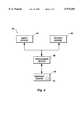
- FIG. 1is an isometric view of a portion of a multi-chip module in accordance with the present invention
- FIG. 2is an isometric view of the multi-chip module of FIG. 1 including an additional stacked die;
- FIGS. 3A and 3Bare respective top plan and isometric views of the multi-chip module of FIG. 1 showing alternative embodiments of the module in detail;
- FIG. 4is a block diagram of an electronic system including the multi-chip module of FIG. 1.
- an inventive Multi-Chip Module (MCM) 10includes a flip-chip integrated circuit (IC) die 12 with flip-chip bumps (not shown) on its front-side surface 16 reflow-soldered in a well-known manner to flip-chip pads (not shown) screen printed on a surface 20 of a printed circuit board (PCB) 22.
- Circuitry (not shown) within the flip-chip IC die 12communicates with external circuitry (not shown) through conductors 24 connected to the flip-chip pads (not shown).
- the present inventionwill be described with respect to the MCM 10, it will be understood by those having skill in the field of the invention that the invention includes within its scope a wide variety of electronic devices other than MCM's, including, for example, memory devices such as Single In-line Memory Modules (SIMM's) and Dual In-line Memory Modules (DIMM's).
- the flip-chip IC die 12may comprise any IC die having flip-chip bumps, and that the flip-chip IC die 12 may be bonded to the flip-chip pads (not shown) using methods other than reflow soldering.
- the flip-chip pads (not shown)may be provided on the surface 20 using a method other than screen printing, such as selective plating, and that the present invention includes within its scope bases other than the PCB 22.
- a wire-bondable IC die 26is stacked on top of the flip-chip IC die 12. This may be done, for example, to increase the amount of Dynamic Random Access Memory (DRAM) provided on the PCB 22 if the IC dice 12 and 26 are DRAM IC dice. It may also be done to replace the flip-chip IC die 12 with the wire-bondable IC die 26 if the flip-chip IC die 12 is defective.
- DRAMDynamic Random Access Memory
- the wire-bondable IC die 26may be any wire-bondable IC die.
- a back-side surface of the wire-bondable IC die 26is attached to a back-side surface of the flip-chip IC die 12 with epoxy 28, and bond pads on a front-side surface of the wire-bondable IC die 26 are wire-bonded to wire-bondable pads 30 screen printed on the surface 20 of the PCB 22.
- the IC dice 12 and 26may be back-bonded using means other than epoxy, and that the wire-bondable pads 30 may be provided on the surface 20 using a method other than screen printing, such as selective plating.
- the wire-bondable IC die 26is being used to replace a defective flip-chip IC die 12, communication between the defective flip-chip IC die 12 and external circuitry (not shown) is interrupted by cutting the conductors 24 at locations proximate to each of the flip-chip pads (not shown).
- the present inventionincludes within its scope other methods for interrupting communication between the flip-chip IC die 12 and external circuitry, including; for example, de-selecting or de-powering the flip-chip IC die 12. With communication between the flip-chip IC die 12 and external circuitry interrupted, the wire-bondable IC die 26 communicates with external circuitry through the conductors 24 without interference from the defective flip-chip IC die 12.
- the present inventionprovides a simple stacking technique for IC dice flip-chip mounted to a PCB or any other base, and the inventive technique is useful for repairing or replacing flip-chip mounted IC dice.
- a method of assembling the MCM 10includes: screen printing or selectively plating the flip-chip pads (not shown) and wire-bondable pads 30; picking and placing the flip-chip IC die 12; reflow soldering the flip-chip bumps (not shown) to the flip-chip pads (not shown); testing the connection between the flip-chip bumps (not shown) and the flip-chip pads and, if the connection fails the test, repairing the connection; underfilling the flip-chip IC die 12; picking and placing the wire-bondable IC die 26; back-bonding the IC dice 12 and 26 to one another with un-cured epoxy; curing the epoxy; wire-bonding the bond pads on the wire-bondable IC die 26 to the wire-bondable pads 30; testing the connection between the bond pads and the wire-bondable pads 30 and, if the connection fails the test, repairing the connection; and encapsulating the IC dice 12 and 26.
- the MCM 10includes an additional IC die 32 back-side attached to the wire-bondable IC die 26 and wire-bonded to the bond pads of the wire-bondable IC die 26.
- the density of dice on the PCB 22is increased.
- the present inventionincludes within its scope multiple dice stacked on top of the wire-bondable IC die 26.
- the IC dice 12 (shown in FIG. 1) and 26are identical with respect to the arrangement of their bond pads and the functions associated with their respective bond pads.
- the bond pads of the flip chip IC die 12 (shown in FIG. 1)are oriented in a "flipped" relationship with respect to the bond pads of the wire-bondable IC die 26. Consequently, the flip chip pads 18 on the PCB 22 are interconnected with the wire-bondable pads 30 on the surface 20 of the PCB 22 so bond pads on each of the dice 12 (shown in FIG. 1) and 26 that are associated with the same function are interconnected, thus allowing both dice 12 and 26 to operate in parallel.
- the flip chip pads 18may be said to then "electrically mirror" the wire bondable pads 30.
- FIG. 3Ait will be understood that a wide variety of interconnection arrangements which vary widely from that shown in FIG. 3A is within the scope of the present invention.
- the IC dice 12 and 26are identical with respect to the arrangement of their bond pads and the functions associated with their respective bond pads.
- the bond pads of the flip chip IC die 12are oriented in a "flipped" relationship with respect to the bond pads of the wire-bondable IC die 26.
- flip chip pads 34 on the PCB 22are interconnected with wire-bondable pads 36 on the PCB 22 through different layers 37 and 38 in the PCB 22 so bond pads on each of the dice 12 and 26 that are associated with the same function are interconnected, thus allowing both dice 12 and 26 to operate in parallel.
- the flip chip pads 34may be said to then "electrically mirror" the wire bondable pads 36.
- multi-layer PCB interconnection arrangementswhich vary widely from that shown in FIG. 3B are within the scope of the present invention.
- the MCM 10is incorporated into a memory device 40 in an electronic system 42 that also includes an input device 44, an output device 46, and a processor device 48. It will be understood that the MCM 10 may alternatively be incorporated into any one or all of the input, output, and processor devices 44, 46, and 48.
Landscapes
- Engineering & Computer Science (AREA)
- Microelectronics & Electronic Packaging (AREA)
- Power Engineering (AREA)
- Computer Hardware Design (AREA)
- Physics & Mathematics (AREA)
- Condensed Matter Physics & Semiconductors (AREA)
- General Physics & Mathematics (AREA)
- Manufacturing & Machinery (AREA)
- Wire Bonding (AREA)
- Semiconductor Integrated Circuits (AREA)
Abstract
Description
Claims (18)
Priority Applications (1)
| Application Number | Priority Date | Filing Date | Title |
|---|---|---|---|
| US08/914,515US5973403A (en) | 1996-11-20 | 1997-08-19 | Device and method for stacking wire-bonded integrated circuit dice on flip-chip bonded integrated circuit dice |
Applications Claiming Priority (2)
| Application Number | Priority Date | Filing Date | Title |
|---|---|---|---|
| US08/752,802US5696031A (en) | 1996-11-20 | 1996-11-20 | Device and method for stacking wire-bonded integrated circuit dice on flip-chip bonded integrated circuit dice |
| US08/914,515US5973403A (en) | 1996-11-20 | 1997-08-19 | Device and method for stacking wire-bonded integrated circuit dice on flip-chip bonded integrated circuit dice |
Related Parent Applications (1)
| Application Number | Title | Priority Date | Filing Date |
|---|---|---|---|
| US08/752,802DivisionUS5696031A (en) | 1996-02-20 | 1996-11-20 | Device and method for stacking wire-bonded integrated circuit dice on flip-chip bonded integrated circuit dice |
Publications (1)
| Publication Number | Publication Date |
|---|---|
| US5973403Atrue US5973403A (en) | 1999-10-26 |
Family
ID=25027913
Family Applications (15)
| Application Number | Title | Priority Date | Filing Date |
|---|---|---|---|
| US08/752,802Expired - LifetimeUS5696031A (en) | 1996-02-20 | 1996-11-20 | Device and method for stacking wire-bonded integrated circuit dice on flip-chip bonded integrated circuit dice |
| US08/914,515Expired - LifetimeUS5973403A (en) | 1996-11-20 | 1997-08-19 | Device and method for stacking wire-bonded integrated circuit dice on flip-chip bonded integrated circuit dice |
| US08/914,719Expired - LifetimeUS6071754A (en) | 1996-02-20 | 1997-08-19 | Device and method for stacking wire-bonded integrated circuit dice on flip-chip bonded integrated circuit dice |
| US09/390,889Expired - LifetimeUS6140149A (en) | 1996-02-20 | 1999-09-07 | Device and method for stacking wire-bonded integrated circuit dice on flip-chip bonded integrated circuit dice |
| US09/642,134Expired - LifetimeUS6399416B1 (en) | 1996-11-20 | 2000-08-18 | Device and method for stacking wire-bonded integrated circuit dice on flip-chip bonded integrated circuit dice |
| US10/156,976Expired - LifetimeUS6605489B2 (en) | 1996-11-20 | 2002-05-29 | Methods for stacking wire-bonded integrated circuit dice on flip-chip bonded integrated circuit dice |
| US10/634,074Expired - Fee RelatedUS6869826B2 (en) | 1996-11-20 | 2003-08-04 | Methods for stacking wire-bonded integrated circuit dice on flip-chip bonded integrated circuit dice |
| US11/086,144Expired - Fee RelatedUS7109059B2 (en) | 1996-11-20 | 2005-03-22 | Methods for stacking wire-bonded integrated circuit dice on flip-chip bonded integrated circuit dice |
| US11/252,389Expired - Fee RelatedUS7282792B2 (en) | 1996-11-20 | 2005-10-18 | Methods for stacking wire-bonded integrated circuit dice on flip-chip bonded integrated circuit dice |
| US11/601,970Expired - Fee RelatedUS7411286B2 (en) | 1996-11-20 | 2006-11-20 | Methods for stacking wire-bonded integrated circuit dice on flip-chip bonded integrated circuit dice |
| US11/601,883Expired - Fee RelatedUS7423338B2 (en) | 1996-11-20 | 2006-11-20 | Methods for stacking wire-bonded integrated circuit dice on flip-chip bonded integrated circuit dice |
| US11/602,051Expired - Fee RelatedUS7423339B2 (en) | 1996-11-20 | 2006-11-20 | Methods for stacking wire-bonded integrated circuit dice on flip-chip bonded integrated circuit dice |
| US11/601,969Expired - Fee RelatedUS7402902B2 (en) | 1996-11-20 | 2006-11-20 | Methods for stacking wire-bonded integrated circuit dice on flip-chip bonded integrated circuit dice |
| US12/197,514Expired - Fee RelatedUS7776652B2 (en) | 1996-11-20 | 2008-08-25 | Methods for stacking wire-bonded integrated circuit dice on flip-chip bonded integrated circuit dice |
| US12/197,453Expired - Fee RelatedUS7812436B2 (en) | 1996-11-20 | 2008-08-25 | Methods for stacking wire-bonded integrated circuit dice on flip-chip bonded integrated circuit dice |
Family Applications Before (1)
| Application Number | Title | Priority Date | Filing Date |
|---|---|---|---|
| US08/752,802Expired - LifetimeUS5696031A (en) | 1996-02-20 | 1996-11-20 | Device and method for stacking wire-bonded integrated circuit dice on flip-chip bonded integrated circuit dice |
Family Applications After (13)
| Application Number | Title | Priority Date | Filing Date |
|---|---|---|---|
| US08/914,719Expired - LifetimeUS6071754A (en) | 1996-02-20 | 1997-08-19 | Device and method for stacking wire-bonded integrated circuit dice on flip-chip bonded integrated circuit dice |
| US09/390,889Expired - LifetimeUS6140149A (en) | 1996-02-20 | 1999-09-07 | Device and method for stacking wire-bonded integrated circuit dice on flip-chip bonded integrated circuit dice |
| US09/642,134Expired - LifetimeUS6399416B1 (en) | 1996-11-20 | 2000-08-18 | Device and method for stacking wire-bonded integrated circuit dice on flip-chip bonded integrated circuit dice |
| US10/156,976Expired - LifetimeUS6605489B2 (en) | 1996-11-20 | 2002-05-29 | Methods for stacking wire-bonded integrated circuit dice on flip-chip bonded integrated circuit dice |
| US10/634,074Expired - Fee RelatedUS6869826B2 (en) | 1996-11-20 | 2003-08-04 | Methods for stacking wire-bonded integrated circuit dice on flip-chip bonded integrated circuit dice |
| US11/086,144Expired - Fee RelatedUS7109059B2 (en) | 1996-11-20 | 2005-03-22 | Methods for stacking wire-bonded integrated circuit dice on flip-chip bonded integrated circuit dice |
| US11/252,389Expired - Fee RelatedUS7282792B2 (en) | 1996-11-20 | 2005-10-18 | Methods for stacking wire-bonded integrated circuit dice on flip-chip bonded integrated circuit dice |
| US11/601,970Expired - Fee RelatedUS7411286B2 (en) | 1996-11-20 | 2006-11-20 | Methods for stacking wire-bonded integrated circuit dice on flip-chip bonded integrated circuit dice |
| US11/601,883Expired - Fee RelatedUS7423338B2 (en) | 1996-11-20 | 2006-11-20 | Methods for stacking wire-bonded integrated circuit dice on flip-chip bonded integrated circuit dice |
| US11/602,051Expired - Fee RelatedUS7423339B2 (en) | 1996-11-20 | 2006-11-20 | Methods for stacking wire-bonded integrated circuit dice on flip-chip bonded integrated circuit dice |
| US11/601,969Expired - Fee RelatedUS7402902B2 (en) | 1996-11-20 | 2006-11-20 | Methods for stacking wire-bonded integrated circuit dice on flip-chip bonded integrated circuit dice |
| US12/197,514Expired - Fee RelatedUS7776652B2 (en) | 1996-11-20 | 2008-08-25 | Methods for stacking wire-bonded integrated circuit dice on flip-chip bonded integrated circuit dice |
| US12/197,453Expired - Fee RelatedUS7812436B2 (en) | 1996-11-20 | 2008-08-25 | Methods for stacking wire-bonded integrated circuit dice on flip-chip bonded integrated circuit dice |
Country Status (1)
| Country | Link |
|---|---|
| US (15) | US5696031A (en) |
Cited By (98)
| Publication number | Priority date | Publication date | Assignee | Title |
|---|---|---|---|---|
| US6175160B1 (en)* | 1999-01-08 | 2001-01-16 | Intel Corporation | Flip-chip having an on-chip cache memory |
| US6258626B1 (en) | 2000-07-06 | 2001-07-10 | Advanced Semiconductor Engineering, Inc. | Method of making stacked chip package |
| US6291884B1 (en)* | 1999-11-09 | 2001-09-18 | Amkor Technology, Inc. | Chip-size semiconductor packages |
| US6331221B1 (en)* | 1998-04-15 | 2001-12-18 | Micron Technology, Inc. | Process for providing electrical connection between a semiconductor die and a semiconductor die receiving member |
| US6335565B1 (en)* | 1996-12-04 | 2002-01-01 | Hitachi, Ltd. | Semiconductor device |
| US6369445B1 (en) | 2000-06-19 | 2002-04-09 | Advantest Corporation | Method and apparatus for edge connection between elements of an integrated circuit |
| US6370029B1 (en)* | 1997-01-15 | 2002-04-09 | Transaction Technology, Inc. | Method and system for creating and using an electrostatic discharge (ESD) protected logotype contact module with a smart card |
| US20020045290A1 (en)* | 1996-02-20 | 2002-04-18 | Michael B. Ball | Flip chip and conventional stack |
| US6376914B2 (en)* | 1999-12-09 | 2002-04-23 | Atmel Corporation | Dual-die integrated circuit package |
| US6395578B1 (en) | 1999-05-20 | 2002-05-28 | Amkor Technology, Inc. | Semiconductor package and method for fabricating the same |
| US6414396B1 (en) | 2000-01-24 | 2002-07-02 | Amkor Technology, Inc. | Package for stacked integrated circuits |
| US6420789B1 (en) | 2000-05-16 | 2002-07-16 | Micron Technology, Inc. | Ball grid array chip packages having improved testing and stacking characteristics |
| US6426559B1 (en) | 2000-06-29 | 2002-07-30 | National Semiconductor Corporation | Miniature 3D multi-chip module |
| US6440775B2 (en) | 2000-06-19 | 2002-08-27 | Advantest Corporation | Method and apparatus for edge connection between elements of an integrated circuit |
| US6441483B1 (en)* | 2001-03-30 | 2002-08-27 | Micron Technology, Inc. | Die stacking scheme |
| US6445594B1 (en)* | 2000-02-10 | 2002-09-03 | Mitsubishi Denki Kabushiki Kaisha | Semiconductor device having stacked semiconductor elements |
| US20020125556A1 (en)* | 2001-03-09 | 2002-09-12 | Oh Kwang Seok | Stacking structure of semiconductor chips and semiconductor package using it |
| US6452278B1 (en) | 2000-06-30 | 2002-09-17 | Amkor Technology, Inc. | Low profile package for plural semiconductor dies |
| US20020130404A1 (en)* | 2001-03-19 | 2002-09-19 | Toshihiro Ushijima | Semiconductor module in which plural semiconductor chips are enclosed in one package |
| US6462421B1 (en) | 2000-04-10 | 2002-10-08 | Advanced Semicondcutor Engineering, Inc. | Multichip module |
| US6469376B2 (en) | 2001-03-09 | 2002-10-22 | Micron Technology Inc. | Die support structure |
| US6492719B2 (en) | 1999-07-30 | 2002-12-10 | Hitachi, Ltd. | Semiconductor device |
| US20030006494A1 (en)* | 2001-07-03 | 2003-01-09 | Lee Sang Ho | Thin profile stackable semiconductor package and method for manufacturing |
| US20030006496A1 (en)* | 2001-03-15 | 2003-01-09 | Venkateshwaran Vaiyapuri | Semiconductor/printed circuit board assembly, and computer system |
| US20030038374A1 (en)* | 2001-08-27 | 2003-02-27 | Shim Jong Bo | Multi-chip package (MCP) with spacer |
| US6528408B2 (en) | 2001-05-21 | 2003-03-04 | Micron Technology, Inc. | Method for bumped die and wire bonded board-on-chip package |
| US6541871B2 (en)* | 1999-11-09 | 2003-04-01 | Advanced Semiconductor Engineering, Inc. | Method for fabricating a stacked chip package |
| US6552416B1 (en) | 2000-09-08 | 2003-04-22 | Amkor Technology, Inc. | Multiple die lead frame package with enhanced die-to-die interconnect routing using internal lead trace wiring |
| US6555917B1 (en) | 2001-10-09 | 2003-04-29 | Amkor Technology, Inc. | Semiconductor package having stacked semiconductor chips and method of making the same |
| US20030080437A1 (en)* | 2001-10-26 | 2003-05-01 | Intel Corporation | Electronic assembly with filled no-flow underfill and methods of manufacture |
| US6583502B2 (en) | 2001-04-17 | 2003-06-24 | Micron Technology, Inc. | Apparatus for package reduction in stacked chip and board assemblies |
| US20030137042A1 (en)* | 2001-06-21 | 2003-07-24 | Mess Leonard E. | Stacked mass storage flash memory package |
| US6605875B2 (en)* | 1999-12-30 | 2003-08-12 | Intel Corporation | Integrated circuit die having bond pads near adjacent sides to allow stacking of dice without regard to dice size |
| US20030199118A1 (en)* | 1999-12-20 | 2003-10-23 | Amkor Technology, Inc. | Wire bonding method for a semiconductor package |
| US6668242B1 (en)* | 1998-09-25 | 2003-12-23 | Infineon Technologies North America Corp. | Emulator chip package that plugs directly into the target system |
| US6674948B2 (en) | 2001-08-13 | 2004-01-06 | Optoic Technology, Inc. | Optoelectronic IC module |
| US20040004286A1 (en)* | 2002-02-07 | 2004-01-08 | Eide Floyd K. | Stackable layers containing ball grid array packages |
| US20040007771A1 (en)* | 1999-08-24 | 2004-01-15 | Amkor Technology, Inc. | Semiconductor package and method for fabricating the smae |
| US20040029315A1 (en)* | 1996-11-20 | 2004-02-12 | Wark James M. | Methods for stacking wire-bonded integrated circuit dice on flip-chip bonded integrated circuit dice |
| US6692979B2 (en) | 2001-08-13 | 2004-02-17 | Optoic Technology, Inc. | Methods of fabricating optoelectronic IC modules |
| US6710454B1 (en) | 2000-02-16 | 2004-03-23 | Micron Technology, Inc. | Adhesive layer for an electronic apparatus having multiple semiconductor devices |
| US6717248B2 (en) | 1999-05-07 | 2004-04-06 | Amkor Technology, Inc. | Semiconductor package and method for fabricating the same |
| US20040070064A1 (en)* | 2002-10-15 | 2004-04-15 | Tae Yamane | Semiconductor device and fabrication method of the same |
| US6737750B1 (en) | 2001-12-07 | 2004-05-18 | Amkor Technology, Inc. | Structures for improving heat dissipation in stacked semiconductor packages |
| US6740970B2 (en)* | 2001-05-15 | 2004-05-25 | Fujitsu Limited | Semiconductor device with stack of semiconductor chips |
| US6759737B2 (en) | 2000-03-25 | 2004-07-06 | Amkor Technology, Inc. | Semiconductor package including stacked chips with aligned input/output pads |
| US6768207B2 (en) | 2002-05-17 | 2004-07-27 | Advanced Semiconductor Engineering Inc. | Multichip wafer-level package and method for manufacturing the same |
| US6798055B2 (en) | 2001-03-12 | 2004-09-28 | Micron Technology | Die support structure |
| EP1501126A1 (en)* | 2003-11-05 | 2005-01-26 | Infineon Technologies AG | Semiconductor chip having a cavity for stacked die application |
| US6858932B2 (en) | 2002-02-07 | 2005-02-22 | Freescale Semiconductor, Inc. | Packaged semiconductor device and method of formation |
| US20050046023A1 (en)* | 2003-08-28 | 2005-03-03 | Renesas Technology Corp. | Semiconductor device |
| US6879047B1 (en) | 2003-02-19 | 2005-04-12 | Amkor Technology, Inc. | Stacking structure for semiconductor devices using a folded over flexible substrate and method therefor |
| US20050156322A1 (en)* | 2001-08-31 | 2005-07-21 | Smith Lee J. | Thin semiconductor package including stacked dies |
| US20050189623A1 (en)* | 2001-03-12 | 2005-09-01 | Salman Akram | Multiple die package |
| US6946323B1 (en) | 2001-11-02 | 2005-09-20 | Amkor Technology, Inc. | Semiconductor package having one or more die stacked on a prepackaged device and method therefor |
| DE102004005586B3 (en)* | 2004-02-04 | 2005-09-29 | Infineon Technologies Ag | Semiconductor device having a semiconductor chip stack on a rewiring plate and producing the same |
| US6982485B1 (en) | 2002-02-13 | 2006-01-03 | Amkor Technology, Inc. | Stacking structure for semiconductor chips and a semiconductor package using it |
| US20060055039A1 (en)* | 2002-02-07 | 2006-03-16 | Floyd Eide | Stackable layer containing ball grid array package |
| US20060102994A1 (en)* | 2004-11-16 | 2006-05-18 | Siliconware Precision Industries Co., Ltd. | Multi-chip semiconductor package and fabrication method thereof |
| US7071574B1 (en)* | 2000-01-17 | 2006-07-04 | Renesas Technology Corp. | Semiconductor device and its wiring method |
| US7154171B1 (en) | 2002-02-22 | 2006-12-26 | Amkor Technology, Inc. | Stacking structure for semiconductor devices using a folded over flexible substrate and method therefor |
| US20070099341A1 (en)* | 2005-09-23 | 2007-05-03 | Lo Wai Y | Method of making stacked die package |
| US7217597B2 (en) | 2004-06-22 | 2007-05-15 | Micron Technology, Inc. | Die stacking scheme |
| US20070136766A1 (en)* | 2005-12-09 | 2007-06-14 | Ryuichi Iwamura | Cross-phase adapter for powerline communications (PLC) network |
| US20070170575A1 (en)* | 2006-01-26 | 2007-07-26 | Samsung Electronics Co., Ltd. | Stack chip and stack chip package having the same |
| USRE40112E1 (en) | 1999-05-20 | 2008-02-26 | Amkor Technology, Inc. | Semiconductor package and method for fabricating the same |
| US20080083978A1 (en)* | 2004-09-21 | 2008-04-10 | Yoshinari Hayashi | Semiconductor device |
| US20090065948A1 (en)* | 2007-09-06 | 2009-03-12 | Micron Technology, Inc. | Package structure for multiple die stack |
| US20090065929A1 (en)* | 2005-03-31 | 2009-03-12 | Kazuhiko Hiranuma | Multi-chip semiconductor device |
| US7633144B1 (en) | 2006-05-24 | 2009-12-15 | Amkor Technology, Inc. | Semiconductor package |
| US7675180B1 (en) | 2006-02-17 | 2010-03-09 | Amkor Technology, Inc. | Stacked electronic component package having film-on-wire spacer |
| US7714426B1 (en) | 2007-07-07 | 2010-05-11 | Keith Gann | Ball grid array package format layers and structure |
| US20100230825A1 (en)* | 2009-03-12 | 2010-09-16 | Von Kaenel Vincent R | Flexible Packaging for Chip-on-Chip and Package-on-Package Technologies |
| US7829991B2 (en) | 1998-06-30 | 2010-11-09 | Micron Technology, Inc. | Stackable ceramic FBGA for high thermal applications |
| US7927919B1 (en)* | 2009-12-03 | 2011-04-19 | Powertech Technology Inc. | Semiconductor packaging method to save interposer |
| US7990727B1 (en) | 2006-04-03 | 2011-08-02 | Aprolase Development Co., Llc | Ball grid array stack |
| US8072082B2 (en) | 2008-04-24 | 2011-12-06 | Micron Technology, Inc. | Pre-encapsulated cavity interposer |
| WO2013052322A3 (en)* | 2011-10-03 | 2013-06-20 | Invensas Corporation | Stub minimization using duplicate sets of terminals for wirebond assemblies without windows |
| US8513813B2 (en) | 2011-10-03 | 2013-08-20 | Invensas Corporation | Stub minimization using duplicate sets of terminals for wirebond assemblies without windows |
| US8525327B2 (en) | 2011-10-03 | 2013-09-03 | Invensas Corporation | Stub minimization for assemblies without wirebonds to package substrate |
| US8659142B2 (en) | 2011-10-03 | 2014-02-25 | Invensas Corporation | Stub minimization for wirebond assemblies without windows |
| US8659139B2 (en) | 2011-10-03 | 2014-02-25 | Invensas Corporation | Stub minimization using duplicate sets of signal terminals in assemblies without wirebonds to package substrate |
| US8670261B2 (en) | 2011-10-03 | 2014-03-11 | Invensas Corporation | Stub minimization using duplicate sets of signal terminals |
| US8759982B2 (en) | 2011-07-12 | 2014-06-24 | Tessera, Inc. | Deskewed multi-die packages |
| US8787034B2 (en) | 2012-08-27 | 2014-07-22 | Invensas Corporation | Co-support system and microelectronic assembly |
| US8823165B2 (en) | 2011-07-12 | 2014-09-02 | Invensas Corporation | Memory module in a package |
| US8848392B2 (en) | 2012-08-27 | 2014-09-30 | Invensas Corporation | Co-support module and microelectronic assembly |
| US8848391B2 (en) | 2012-08-27 | 2014-09-30 | Invensas Corporation | Co-support component and microelectronic assembly |
| US8917532B2 (en) | 2011-10-03 | 2014-12-23 | Invensas Corporation | Stub minimization with terminal grids offset from center of package |
| US8981547B2 (en) | 2011-10-03 | 2015-03-17 | Invensas Corporation | Stub minimization for multi-die wirebond assemblies with parallel windows |
| US9070423B2 (en) | 2013-06-11 | 2015-06-30 | Invensas Corporation | Single package dual channel memory with co-support |
| US9123555B2 (en) | 2013-10-25 | 2015-09-01 | Invensas Corporation | Co-support for XFD packaging |
| US9281296B2 (en) | 2014-07-31 | 2016-03-08 | Invensas Corporation | Die stacking techniques in BGA memory package for small footprint CPU and memory motherboard design |
| US9368477B2 (en) | 2012-08-27 | 2016-06-14 | Invensas Corporation | Co-support circuit panel and microelectronic packages |
| US9466545B1 (en) | 2007-02-21 | 2016-10-11 | Amkor Technology, Inc. | Semiconductor package in package |
| US9484080B1 (en) | 2015-11-09 | 2016-11-01 | Invensas Corporation | High-bandwidth memory application with controlled impedance loading |
| US9679613B1 (en) | 2016-05-06 | 2017-06-13 | Invensas Corporation | TFD I/O partition for high-speed, high-density applications |
| US9691437B2 (en) | 2014-09-25 | 2017-06-27 | Invensas Corporation | Compact microelectronic assembly having reduced spacing between controller and memory packages |
Families Citing this family (97)
| Publication number | Priority date | Publication date | Assignee | Title |
|---|---|---|---|---|
| US5657206A (en)* | 1994-06-23 | 1997-08-12 | Cubic Memory, Inc. | Conductive epoxy flip-chip package and method |
| US5991850A (en) | 1996-08-15 | 1999-11-23 | Micron Technology, Inc. | Synchronous DRAM modules including multiple clock out signals for increasing processing speed |
| JP3241639B2 (en)* | 1997-06-30 | 2001-12-25 | 日本電気株式会社 | Multi-chip module cooling structure and method of manufacturing the same |
| US6159764A (en) | 1997-07-02 | 2000-12-12 | Micron Technology, Inc. | Varied-thickness heat sink for integrated circuit (IC) packages and method of fabricating IC packages |
| FR2785722A1 (en)* | 1998-11-06 | 2000-05-12 | Bull Sa | THREE-DIMENSIONAL INTERCONNECTION STRUCTURE OF MULTIPLE CIRCUITS TO FORM A MULTI-COMPONENT PACKAGE |
| US7157314B2 (en) | 1998-11-16 | 2007-01-02 | Sandisk Corporation | Vertically stacked field programmable nonvolatile memory and method of fabrication |
| US6122187A (en) | 1998-11-23 | 2000-09-19 | Micron Technology, Inc. | Stacked integrated circuits |
| US6507117B1 (en)* | 1999-01-29 | 2003-01-14 | Rohm Co., Ltd. | Semiconductor chip and multichip-type semiconductor device |
| US6407450B1 (en)* | 1999-07-15 | 2002-06-18 | Altera Corporation | Semiconductor package with universal substrate for electrically interfacing with different sized chips that have different logic functions |
| SG83742A1 (en)* | 1999-08-17 | 2001-10-16 | Micron Technology Inc | Multi-chip module with extension |
| SG87046A1 (en)* | 1999-08-17 | 2002-03-19 | Micron Technology Inc | Multi-chip module with stacked dice |
| JP3765952B2 (en)* | 1999-10-19 | 2006-04-12 | 富士通株式会社 | Semiconductor device |
| US6621155B1 (en) | 1999-12-23 | 2003-09-16 | Rambus Inc. | Integrated circuit device having stacked dies and impedance balanced transmission lines |
| US8575719B2 (en) | 2000-04-28 | 2013-11-05 | Sandisk 3D Llc | Silicon nitride antifuse for use in diode-antifuse memory arrays |
| US6888750B2 (en) | 2000-04-28 | 2005-05-03 | Matrix Semiconductor, Inc. | Nonvolatile memory on SOI and compound semiconductor substrates and method of fabrication |
| US6417462B1 (en)* | 2000-06-19 | 2002-07-09 | Intel Corporation | Low cost and high speed 3-load printed wiring board bus topology |
| KR100821456B1 (en) | 2000-08-14 | 2008-04-11 | 샌디스크 쓰리디 엘엘씨 | Dense array and charge storage device and manufacturing method thereof |
| JP3831593B2 (en)* | 2000-09-21 | 2006-10-11 | 三洋電機株式会社 | Multi-chip module |
| US6611434B1 (en)* | 2000-10-30 | 2003-08-26 | Siliconware Precision Industries Co., Ltd. | Stacked multi-chip package structure with on-chip integration of passive component |
| US20020121693A1 (en) | 2000-12-11 | 2002-09-05 | Milla Juan G. | Stacked die package |
| US6900549B2 (en)* | 2001-01-17 | 2005-05-31 | Micron Technology, Inc. | Semiconductor assembly without adhesive fillets |
| US7352199B2 (en) | 2001-02-20 | 2008-04-01 | Sandisk Corporation | Memory card with enhanced testability and methods of making and using the same |
| US6897514B2 (en) | 2001-03-28 | 2005-05-24 | Matrix Semiconductor, Inc. | Two mask floating gate EEPROM and method of making |
| JP3839323B2 (en)* | 2001-04-06 | 2006-11-01 | 株式会社ルネサステクノロジ | Manufacturing method of semiconductor device |
| US7504481B2 (en)* | 2001-08-02 | 2009-03-17 | Bristol-Meyers Squibb Company | TRP channel family member, LTRPC3 polypeptides |
| US6593624B2 (en) | 2001-09-25 | 2003-07-15 | Matrix Semiconductor, Inc. | Thin film transistors with vertically offset drain regions |
| US6841813B2 (en) | 2001-08-13 | 2005-01-11 | Matrix Semiconductor, Inc. | TFT mask ROM and method for making same |
| US6843421B2 (en) | 2001-08-13 | 2005-01-18 | Matrix Semiconductor, Inc. | Molded memory module and method of making the module absent a substrate support |
| US6525953B1 (en) | 2001-08-13 | 2003-02-25 | Matrix Semiconductor, Inc. | Vertically-stacked, field-programmable, nonvolatile memory and method of fabrication |
| US6624485B2 (en) | 2001-11-05 | 2003-09-23 | Matrix Semiconductor, Inc. | Three-dimensional, mask-programmed read only memory |
| KR100426608B1 (en) | 2001-11-20 | 2004-04-08 | 삼성전자주식회사 | Center pad type integrated circuit chip that means for jumpering is mounted on the active layer and manufacturing method thereof and multi chip package |
| US6781239B1 (en)* | 2001-12-05 | 2004-08-24 | National Semiconductor Corporation | Integrated circuit and method of forming the integrated circuit having a die with high Q inductors and capacitors attached to a die with a circuit as a flip chip |
| US6731011B2 (en)* | 2002-02-19 | 2004-05-04 | Matrix Semiconductor, Inc. | Memory module having interconnected and stacked integrated circuits |
| US6853049B2 (en) | 2002-03-13 | 2005-02-08 | Matrix Semiconductor, Inc. | Silicide-silicon oxide-semiconductor antifuse device and method of making |
| US6542393B1 (en) | 2002-04-24 | 2003-04-01 | Ma Laboratories, Inc. | Dual-bank memory module with stacked DRAM chips having a concave-shaped re-route PCB in-between |
| US6682955B2 (en)* | 2002-05-08 | 2004-01-27 | Micron Technology, Inc. | Stacked die module and techniques for forming a stacked die module |
| US6737675B2 (en) | 2002-06-27 | 2004-05-18 | Matrix Semiconductor, Inc. | High density 3D rail stack arrays |
| US6762472B2 (en) | 2002-08-30 | 2004-07-13 | Agilent Technologies, Inc. | Signal communication structures |
| US20070197030A1 (en)* | 2002-10-10 | 2007-08-23 | Samsung Electronics Co., Ltd. | Center pad type ic chip with jumpers, method of processing the same and multi chip package |
| JP4149289B2 (en)* | 2003-03-12 | 2008-09-10 | 株式会社ルネサステクノロジ | Semiconductor device |
| US6853064B2 (en) | 2003-05-12 | 2005-02-08 | Micron Technology, Inc. | Semiconductor component having stacked, encapsulated dice |
| US9010645B2 (en) | 2003-06-13 | 2015-04-21 | Michael Arnouse | Portable computing system and portable computer for use with same |
| JP3804649B2 (en)* | 2003-09-19 | 2006-08-02 | 株式会社村田製作所 | Electronic circuit device manufacturing method and electronic circuit device |
| JP3880572B2 (en)* | 2003-10-31 | 2007-02-14 | 沖電気工業株式会社 | Semiconductor chip and semiconductor device |
| US7245021B2 (en)* | 2004-04-13 | 2007-07-17 | Vertical Circuits, Inc. | Micropede stacked die component assembly |
| US7705432B2 (en) | 2004-04-13 | 2010-04-27 | Vertical Circuits, Inc. | Three dimensional six surface conformal die coating |
| US7215018B2 (en) | 2004-04-13 | 2007-05-08 | Vertical Circuits, Inc. | Stacked die BGA or LGA component assembly |
| JP2006080145A (en)* | 2004-09-07 | 2006-03-23 | Nec Electronics Corp | Chip-on-chip semiconductor integrated circuit device |
| TWI249831B (en)* | 2005-02-21 | 2006-02-21 | Touch Micro System Tech | Chip type micro connector and method of packaging the sane |
| US20080024998A1 (en)* | 2005-07-20 | 2008-01-31 | Shih-Ping Hsu | Substrate structure integrated with passive components |
| US20080023821A1 (en)* | 2005-07-20 | 2008-01-31 | Shih-Ping Hsu | Substrate structure integrated with passive components |
| JP4863746B2 (en)* | 2006-03-27 | 2012-01-25 | 富士通株式会社 | Semiconductor device and manufacturing method thereof |
| TWI304719B (en)* | 2006-10-25 | 2008-12-21 | Phoenix Prec Technology Corp | Circuit board structure having embedded compacitor and fabrication method thereof |
| US7768117B2 (en)* | 2007-05-30 | 2010-08-03 | Tessera, Inc. | Microelectronic package having interconnected redistribution paths |
| KR100891537B1 (en) | 2007-12-13 | 2009-04-03 | 주식회사 하이닉스반도체 | Substrate for semiconductor package and semiconductor package having same |
| US7955953B2 (en) | 2007-12-17 | 2011-06-07 | Freescale Semiconductor, Inc. | Method of forming stacked die package |
| US7919845B2 (en)* | 2007-12-20 | 2011-04-05 | Xilinx, Inc. | Formation of a hybrid integrated circuit device |
| US11113228B2 (en) | 2008-02-13 | 2021-09-07 | Arnouse Digital Devices Corporation | Portable computing system and portable computer for use with same |
| USRE49124E1 (en) | 2008-02-13 | 2022-07-05 | Arnouse Digital Devices Corp. | Mobile data center |
| US10235323B2 (en) | 2008-02-13 | 2019-03-19 | Michael Arnouse | Portable computing system and portable computer for use with same |
| JP2009246218A (en) | 2008-03-31 | 2009-10-22 | Renesas Technology Corp | Semiconductor device and method for manufacturing the same |
| US8480499B2 (en)* | 2008-04-30 | 2013-07-09 | Scientific Games Holdings Limited | System and method for game brokering |
| US8127185B2 (en)* | 2009-01-23 | 2012-02-28 | Micron Technology, Inc. | Memory devices and methods for managing error regions |
| US20110147069A1 (en)* | 2009-12-18 | 2011-06-23 | International Business Machines Corporation | Multi-tiered Circuit Board and Method of Manufacture |
| ITMI20101415A1 (en)* | 2010-07-29 | 2012-01-30 | St Microelectronics Srl | TRACEABLE INTEGRATED CIRCUITS AND RELATED PRODUCTION METHOD |
| JP2013004572A (en)* | 2011-06-13 | 2013-01-07 | Mitsubishi Electric Corp | Semiconductor device manufacturing method |
| US9947688B2 (en) | 2011-06-22 | 2018-04-17 | Psemi Corporation | Integrated circuits with components on both sides of a selected substrate and methods of fabrication |
| US20120326304A1 (en)* | 2011-06-24 | 2012-12-27 | Warren Robert W | Externally Wire Bondable Chip Scale Package in a System-in-Package Module |
| US20130015871A1 (en)* | 2011-07-11 | 2013-01-17 | Cascade Microtech, Inc. | Systems, devices, and methods for two-sided testing of electronic devices |
| US8611437B2 (en) | 2012-01-26 | 2013-12-17 | Nvidia Corporation | Ground referenced single-ended signaling |
| US9338036B2 (en) | 2012-01-30 | 2016-05-10 | Nvidia Corporation | Data-driven charge-pump transmitter for differential signaling |
| US10101769B2 (en) | 2012-04-10 | 2018-10-16 | Michael Arnouse | Mobile data center |
| US10128219B2 (en) | 2012-04-25 | 2018-11-13 | Texas Instruments Incorporated | Multi-chip module including stacked power devices with metal clip |
| JP2014138119A (en) | 2013-01-17 | 2014-07-28 | Sony Corp | Semiconductor device and semiconductor device manufacturing method |
| US8686552B1 (en) | 2013-03-14 | 2014-04-01 | Palo Alto Research Center Incorporated | Multilevel IC package using interconnect springs |
| US9076551B2 (en) | 2013-03-15 | 2015-07-07 | Nvidia Corporation | Multi-phase ground-referenced single-ended signaling |
| US9170980B2 (en) | 2013-03-15 | 2015-10-27 | Nvidia Corporation | Ground-referenced single-ended signaling connected graphics processing unit multi-chip module |
| US9153539B2 (en) | 2013-03-15 | 2015-10-06 | Nvidia Corporation | Ground-referenced single-ended signaling connected graphics processing unit multi-chip module |
| US9147447B2 (en) | 2013-03-15 | 2015-09-29 | Nvidia Corporation | Ground-referenced single-ended memory interconnect |
| US9153314B2 (en) | 2013-03-15 | 2015-10-06 | Nvidia Corporation | Ground-referenced single-ended memory interconnect |
| US9171607B2 (en) | 2013-03-15 | 2015-10-27 | Nvidia Corporation | Ground-referenced single-ended system-on-package |
| US8854123B1 (en)* | 2013-03-15 | 2014-10-07 | Nvidia Corporation | On-package multiprocessor ground-referenced single-ended interconnect |
| TWI522012B (en)* | 2013-11-19 | 2016-02-11 | 碩頡科技股份有限公司 | Integrated light source driving circuit and light source module using the same |
| CN104681550A (en)* | 2013-11-26 | 2015-06-03 | 硕颉科技股份有限公司 | Integrated light source driving circuit and light source module using it |
| US9129962B1 (en) | 2014-05-07 | 2015-09-08 | Mediatek Inc. | Bonding pad arrangment design for multi-die semiconductor package structure |
| US9627395B2 (en) | 2015-02-11 | 2017-04-18 | Sandisk Technologies Llc | Enhanced channel mobility three-dimensional memory structure and method of making thereof |
| US9478495B1 (en) | 2015-10-26 | 2016-10-25 | Sandisk Technologies Llc | Three dimensional memory device containing aluminum source contact via structure and method of making thereof |
| US10002100B2 (en) | 2016-02-02 | 2018-06-19 | Xilinx, Inc. | Active-by-active programmable device |
| US10042806B2 (en) | 2016-02-02 | 2018-08-07 | Xilinx, Inc. | System-level interconnect ring for a programmable integrated circuit |
| WO2017135967A1 (en)* | 2016-02-05 | 2017-08-10 | Hewlett Packard Enterprise Development Lp | Dual in-line memory module |
| US11239158B1 (en)* | 2020-10-08 | 2022-02-01 | Qualcomm Incorporated | Wire bond inductor structures for flip chip dies |
| KR20220058702A (en) | 2020-10-29 | 2022-05-10 | 삼성전자주식회사 | Semiconductor package |
| US12021061B2 (en) | 2021-03-04 | 2024-06-25 | Western Digital Technologies, Inc. | Packaged memory device with flip chip and wire bond dies |
| US12288770B2 (en) | 2022-04-25 | 2025-04-29 | Nxp B.V. | Semiconductor packages with embedded wiring on re-distributed bumps |
| US20240079369A1 (en)* | 2022-09-06 | 2024-03-07 | Micron Technology, Inc. | Connecting semiconductor dies through traces |
| TWI822504B (en)* | 2022-12-05 | 2023-11-11 | 勤誠興業股份有限公司 | Printed circuit board |
| US12400942B2 (en) | 2023-05-08 | 2025-08-26 | Bae Systems Information And Electronic Systems Integration Inc. | Interposer for implementing flip-chip dies in wirebonded circuit assemblies |
Citations (22)
| Publication number | Priority date | Publication date | Assignee | Title |
|---|---|---|---|---|
| US4447857A (en)* | 1981-12-09 | 1984-05-08 | International Business Machines Corporation | Substrate with multiple type connections |
| US4567643A (en)* | 1983-10-24 | 1986-02-04 | Sintra-Alcatel | Method of replacing an electronic component connected to conducting tracks on a support substrate |
| US4991000A (en)* | 1989-08-31 | 1991-02-05 | Bone Robert L | Vertically interconnected integrated circuit chip system |
| US5008736A (en)* | 1989-11-20 | 1991-04-16 | Motorola, Inc. | Thermal protection method for a power device |
| US5228192A (en)* | 1990-10-29 | 1993-07-20 | Harris Corporation | Method of manufacturing a multi-layered ic packaging assembly |
| US5252857A (en)* | 1991-08-05 | 1993-10-12 | International Business Machines Corporation | Stacked DCA memory chips |
| US5291064A (en)* | 1991-04-16 | 1994-03-01 | Nec Corporation | Package structure for semiconductor device having a flexible wiring circuit member spaced from the package casing |
| US5311059A (en)* | 1992-01-24 | 1994-05-10 | Motorola, Inc. | Backplane grounding for flip-chip integrated circuit |
| US5323060A (en)* | 1993-06-02 | 1994-06-21 | Micron Semiconductor, Inc. | Multichip module having a stacked chip arrangement |
| US5355283A (en)* | 1993-04-14 | 1994-10-11 | Amkor Electronics, Inc. | Ball grid array with via interconnection |
| US5394303A (en)* | 1992-09-11 | 1995-02-28 | Kabushiki Kaisha Toshiba | Semiconductor device |
| US5399903A (en)* | 1990-08-15 | 1995-03-21 | Lsi Logic Corporation | Semiconductor device having an universal die size inner lead layout |
| US5399898A (en)* | 1992-07-17 | 1995-03-21 | Lsi Logic Corporation | Multi-chip semiconductor arrangements using flip chip dies |
| US5422435A (en)* | 1992-05-22 | 1995-06-06 | National Semiconductor Corporation | Stacked multi-chip modules and method of manufacturing |
| US5434745A (en)* | 1994-07-26 | 1995-07-18 | White Microelectronics Div. Of Bowmar Instrument Corp. | Stacked silicon die carrier assembly |
| US5436203A (en)* | 1994-07-05 | 1995-07-25 | Motorola, Inc. | Shielded liquid encapsulated semiconductor device and method for making the same |
| US5467253A (en)* | 1994-06-30 | 1995-11-14 | Motorola, Inc. | Semiconductor chip package and method of forming |
| US5468999A (en)* | 1994-05-26 | 1995-11-21 | Motorola, Inc. | Liquid encapsulated ball grid array semiconductor device with fine pitch wire bonding |
| US5500289A (en)* | 1994-08-15 | 1996-03-19 | Iscar Ltd. | Tungsten-based cemented carbide powder mix and cemented carbide products made therefrom |
| US5508561A (en)* | 1993-11-15 | 1996-04-16 | Nec Corporation | Apparatus for forming a double-bump structure used for flip-chip mounting |
| US5514907A (en)* | 1995-03-21 | 1996-05-07 | Simple Technology Incorporated | Apparatus for stacking semiconductor chips |
| US5527740A (en)* | 1994-06-28 | 1996-06-18 | Intel Corporation | Manufacturing dual sided wire bonded integrated circuit chip packages using offset wire bonds and support block cavities |
Family Cites Families (33)
| Publication number | Priority date | Publication date | Assignee | Title |
|---|---|---|---|---|
| US4247596A (en) | 1979-05-10 | 1981-01-27 | Yee Tin B | Electrical fiber conductor |
| US4377619A (en) | 1981-05-08 | 1983-03-22 | Bell Telephone Laboratories, Incorporated | Prevention of surface mass migration by means of a polymeric surface coating |
| JPS628534A (en) | 1985-07-04 | 1987-01-16 | Seiko Epson Corp | Semiconductor mounting structure |
| JPS63104343A (en) | 1986-10-21 | 1988-05-09 | Mitsubishi Electric Corp | semiconductor equipment |
| JPS63179537A (en) | 1987-01-21 | 1988-07-23 | Fujitsu Ltd | Mounting method for semiconductor devices |
| JPH01303730A (en) | 1988-06-01 | 1989-12-07 | Hitachi Ltd | Semiconductor element mounting structure and its manufacturing method |
| US5012323A (en) | 1989-11-20 | 1991-04-30 | Micron Technology, Inc. | Double-die semiconductor package having a back-bonded die and a face-bonded die interconnected on a single leadframe |
| US5281846A (en) | 1990-05-29 | 1994-01-25 | Texas Instruments Deutschland Gmbh | Electronic device having a discrete capacitor adherently mounted to a lead frame |
| JPH0513665A (en) | 1991-06-28 | 1993-01-22 | Nec Corp | Method for mounting tab chip |
| CA2072377A1 (en) | 1991-07-12 | 1993-01-13 | Masanori Nishiguchi | Semiconductor chip module and method of manufacturing the same |
| JPH0715969B2 (en) | 1991-09-30 | 1995-02-22 | インターナショナル・ビジネス・マシーンズ・コーポレイション | Multi-chip integrated circuit package and system thereof |
| US5128831A (en) | 1991-10-31 | 1992-07-07 | Micron Technology, Inc. | High-density electronic package comprising stacked sub-modules which are electrically interconnected by solder-filled vias |
| WO1993023982A1 (en)* | 1992-05-11 | 1993-11-25 | Nchip, Inc. | Stacked devices for multichip modules |
| US5279991A (en) | 1992-05-15 | 1994-01-18 | Irvine Sensors Corporation | Method for fabricating stacks of IC chips by segmenting a larger stack |
| US6077725A (en)* | 1992-09-03 | 2000-06-20 | Lucent Technologies Inc | Method for assembling multichip modules |
| US5291061A (en) | 1993-04-06 | 1994-03-01 | Micron Semiconductor, Inc. | Multi-chip stacked devices |
| US5322207A (en) | 1993-05-03 | 1994-06-21 | Micron Semiconductor Inc. | Method and apparatus for wire bonding semiconductor dice to a leadframe |
| US5468099A (en)* | 1993-08-11 | 1995-11-21 | Vought Aircraft Company | Seam tracking drilling machine |
| US5483024A (en) | 1993-10-08 | 1996-01-09 | Texas Instruments Incorporated | High density semiconductor package |
| US5600175A (en) | 1994-07-27 | 1997-02-04 | Texas Instruments Incorporated | Apparatus and method for flat circuit assembly |
| US5721452A (en) | 1995-08-16 | 1998-02-24 | Micron Technology, Inc. | Angularly offset stacked die multichip device and method of manufacture |
| US5874781A (en) | 1995-08-16 | 1999-02-23 | Micron Technology, Inc. | Angularly offset stacked die multichip device and method of manufacture |
| US5886412A (en) | 1995-08-16 | 1999-03-23 | Micron Technology, Inc. | Angularly offset and recessed stacked die multichip device |
| US5851845A (en) | 1995-12-18 | 1998-12-22 | Micron Technology, Inc. | Process for packaging a semiconductor die using dicing and testing |
| US5855821A (en)* | 1995-12-22 | 1999-01-05 | Johnson Matthey, Inc. | Materials for semiconductor device assemblies |
| US6002177A (en) | 1995-12-27 | 1999-12-14 | International Business Machines Corporation | High density integrated circuit packaging with chip stacking and via interconnections |
| US5696031A (en) | 1996-11-20 | 1997-12-09 | Micron Technology, Inc. | Device and method for stacking wire-bonded integrated circuit dice on flip-chip bonded integrated circuit dice |
| US5952725A (en)* | 1996-02-20 | 1999-09-14 | Micron Technology, Inc. | Stacked semiconductor devices |
| US7166495B2 (en)* | 1996-02-20 | 2007-01-23 | Micron Technology, Inc. | Method of fabricating a multi-die semiconductor package assembly |
| US5917242A (en)* | 1996-05-20 | 1999-06-29 | Micron Technology, Inc. | Combination of semiconductor interconnect |
| US5923955A (en)* | 1998-05-28 | 1999-07-13 | Xerox Corporation | Fine flip chip interconnection |
| US6215193B1 (en) | 1999-04-21 | 2001-04-10 | Advanced Semiconductor Engineering, Inc. | Multichip modules and manufacturing method therefor |
| JP2001015553A (en) | 1999-06-29 | 2001-01-19 | Rohm Co Ltd | Manufacture of semiconductor device |
- 1996
- 1996-11-20USUS08/752,802patent/US5696031A/ennot_activeExpired - Lifetime
- 1997
- 1997-08-19USUS08/914,515patent/US5973403A/ennot_activeExpired - Lifetime
- 1997-08-19USUS08/914,719patent/US6071754A/ennot_activeExpired - Lifetime
- 1999
- 1999-09-07USUS09/390,889patent/US6140149A/ennot_activeExpired - Lifetime
- 2000
- 2000-08-18USUS09/642,134patent/US6399416B1/ennot_activeExpired - Lifetime
- 2002
- 2002-05-29USUS10/156,976patent/US6605489B2/ennot_activeExpired - Lifetime
- 2003
- 2003-08-04USUS10/634,074patent/US6869826B2/ennot_activeExpired - Fee Related
- 2005
- 2005-03-22USUS11/086,144patent/US7109059B2/ennot_activeExpired - Fee Related
- 2005-10-18USUS11/252,389patent/US7282792B2/ennot_activeExpired - Fee Related
- 2006
- 2006-11-20USUS11/601,970patent/US7411286B2/ennot_activeExpired - Fee Related
- 2006-11-20USUS11/601,883patent/US7423338B2/ennot_activeExpired - Fee Related
- 2006-11-20USUS11/602,051patent/US7423339B2/ennot_activeExpired - Fee Related
- 2006-11-20USUS11/601,969patent/US7402902B2/ennot_activeExpired - Fee Related
- 2008
- 2008-08-25USUS12/197,514patent/US7776652B2/ennot_activeExpired - Fee Related
- 2008-08-25USUS12/197,453patent/US7812436B2/ennot_activeExpired - Fee Related
Patent Citations (24)
| Publication number | Priority date | Publication date | Assignee | Title |
|---|---|---|---|---|
| US4447857A (en)* | 1981-12-09 | 1984-05-08 | International Business Machines Corporation | Substrate with multiple type connections |
| US4567643A (en)* | 1983-10-24 | 1986-02-04 | Sintra-Alcatel | Method of replacing an electronic component connected to conducting tracks on a support substrate |
| US4991000A (en)* | 1989-08-31 | 1991-02-05 | Bone Robert L | Vertically interconnected integrated circuit chip system |
| US5008736A (en)* | 1989-11-20 | 1991-04-16 | Motorola, Inc. | Thermal protection method for a power device |
| US5399903A (en)* | 1990-08-15 | 1995-03-21 | Lsi Logic Corporation | Semiconductor device having an universal die size inner lead layout |
| US5228192A (en)* | 1990-10-29 | 1993-07-20 | Harris Corporation | Method of manufacturing a multi-layered ic packaging assembly |
| US5291064A (en)* | 1991-04-16 | 1994-03-01 | Nec Corporation | Package structure for semiconductor device having a flexible wiring circuit member spaced from the package casing |
| US5252857A (en)* | 1991-08-05 | 1993-10-12 | International Business Machines Corporation | Stacked DCA memory chips |
| US5311059A (en)* | 1992-01-24 | 1994-05-10 | Motorola, Inc. | Backplane grounding for flip-chip integrated circuit |
| US5495398A (en)* | 1992-05-22 | 1996-02-27 | National Semiconductor Corporation | Stacked multi-chip modules and method of manufacturing |
| US5502289A (en)* | 1992-05-22 | 1996-03-26 | National Semiconductor Corporation | Stacked multi-chip modules and method of manufacturing |
| US5422435A (en)* | 1992-05-22 | 1995-06-06 | National Semiconductor Corporation | Stacked multi-chip modules and method of manufacturing |
| US5399898A (en)* | 1992-07-17 | 1995-03-21 | Lsi Logic Corporation | Multi-chip semiconductor arrangements using flip chip dies |
| US5394303A (en)* | 1992-09-11 | 1995-02-28 | Kabushiki Kaisha Toshiba | Semiconductor device |
| US5355283A (en)* | 1993-04-14 | 1994-10-11 | Amkor Electronics, Inc. | Ball grid array with via interconnection |
| US5323060A (en)* | 1993-06-02 | 1994-06-21 | Micron Semiconductor, Inc. | Multichip module having a stacked chip arrangement |
| US5508561A (en)* | 1993-11-15 | 1996-04-16 | Nec Corporation | Apparatus for forming a double-bump structure used for flip-chip mounting |
| US5468999A (en)* | 1994-05-26 | 1995-11-21 | Motorola, Inc. | Liquid encapsulated ball grid array semiconductor device with fine pitch wire bonding |
| US5527740A (en)* | 1994-06-28 | 1996-06-18 | Intel Corporation | Manufacturing dual sided wire bonded integrated circuit chip packages using offset wire bonds and support block cavities |
| US5467253A (en)* | 1994-06-30 | 1995-11-14 | Motorola, Inc. | Semiconductor chip package and method of forming |
| US5436203A (en)* | 1994-07-05 | 1995-07-25 | Motorola, Inc. | Shielded liquid encapsulated semiconductor device and method for making the same |
| US5434745A (en)* | 1994-07-26 | 1995-07-18 | White Microelectronics Div. Of Bowmar Instrument Corp. | Stacked silicon die carrier assembly |
| US5500289A (en)* | 1994-08-15 | 1996-03-19 | Iscar Ltd. | Tungsten-based cemented carbide powder mix and cemented carbide products made therefrom |
| US5514907A (en)* | 1995-03-21 | 1996-05-07 | Simple Technology Incorporated | Apparatus for stacking semiconductor chips |
Cited By (255)
| Publication number | Priority date | Publication date | Assignee | Title |
|---|---|---|---|---|
| US20020045290A1 (en)* | 1996-02-20 | 2002-04-18 | Michael B. Ball | Flip chip and conventional stack |
| US7166495B2 (en) | 1996-02-20 | 2007-01-23 | Micron Technology, Inc. | Method of fabricating a multi-die semiconductor package assembly |
| US20070117266A1 (en)* | 1996-02-20 | 2007-05-24 | Ball Michael B | Method of fabricating a multi-die semiconductor package assembly |
| US7402902B2 (en) | 1996-11-20 | 2008-07-22 | Micron Technology, Inc. | Methods for stacking wire-bonded integrated circuit dice on flip-chip bonded integrated circuit dice |
| US20080311702A1 (en)* | 1996-11-20 | 2008-12-18 | Micron Technology, Inc. | Methods for stacking wire-bonded integrated circuit dice on flip-chip bonded integrated circuit dice |
| US20070063326A1 (en)* | 1996-11-20 | 2007-03-22 | Wark James M | Methods for stacking wire-bonded integrated circuit dice on flip-chip bonded integrated circuit dice |
| US20070063229A1 (en)* | 1996-11-20 | 2007-03-22 | Wark James M | Methods for stacking wire-bonded integrated circuit dice on flip-chip bonded integrated circuit dice |
| US20070063328A1 (en)* | 1996-11-20 | 2007-03-22 | Wark James M | Methods for stacking wire-bonded integrated circuit dice on flip-chip bonded integrated circuit dice |
| US20040029315A1 (en)* | 1996-11-20 | 2004-02-12 | Wark James M. | Methods for stacking wire-bonded integrated circuit dice on flip-chip bonded integrated circuit dice |
| US20070063327A1 (en)* | 1996-11-20 | 2007-03-22 | Wark James M | Methods for stacking wire-bonded integrated circuit dice on flip-chip bonded integrated circuit dice |
| US7282792B2 (en) | 1996-11-20 | 2007-10-16 | Micron Technology, Inc. | Methods for stacking wire-bonded integrated circuit dice on flip-chip bonded integrated circuit dice |
| US7776652B2 (en) | 1996-11-20 | 2010-08-17 | Micron Technology, Inc. | Methods for stacking wire-bonded integrated circuit dice on flip-chip bonded integrated circuit dice |
| US7812436B2 (en) | 1996-11-20 | 2010-10-12 | Micron Technology, Inc. | Methods for stacking wire-bonded integrated circuit dice on flip-chip bonded integrated circuit dice |
| US7411286B2 (en) | 1996-11-20 | 2008-08-12 | Micron Technology, Inc. | Methods for stacking wire-bonded integrated circuit dice on flip-chip bonded integrated circuit dice |
| US6869826B2 (en) | 1996-11-20 | 2005-03-22 | Micron Technology, Inc. | Methods for stacking wire-bonded integrated circuit dice on flip-chip bonded integrated circuit dice |
| US7109059B2 (en) | 1996-11-20 | 2006-09-19 | Micron Technology, Inc. | Methods for stacking wire-bonded integrated circuit dice on flip-chip bonded integrated circuit dice |
| US7423339B2 (en) | 1996-11-20 | 2008-09-09 | Mircon Technology, Inc. | Methods for stacking wire-bonded integrated circuit dice on flip-chip bonded integrated circuit dice |
| US20060033194A1 (en)* | 1996-11-20 | 2006-02-16 | Wark James M | Methods for stacking wire-bonded integrated circuit dice on flip-chip bonded integrated circuit dice |
| US20050161796A1 (en)* | 1996-11-20 | 2005-07-28 | Wark James M. | Methods for stacking wire-bonded integrated circuit dice on flip-chip bonded integrated circuit dice |
| US20080315435A1 (en)* | 1996-11-20 | 2008-12-25 | Micron Technology, Inc. | Methods for stacking wire-bonded integrated circuit dice on flip-chip bonded integrated circuit dice |
| US7423338B2 (en) | 1996-11-20 | 2008-09-09 | Micron Technology, Inc. | Methods for stacking wire-bonded integrated circuit dice on flip-chip bonded integrated circuit dice |
| US6335565B1 (en)* | 1996-12-04 | 2002-01-01 | Hitachi, Ltd. | Semiconductor device |
| US20050146008A1 (en)* | 1996-12-04 | 2005-07-07 | Renesas Technology Corp. | Semiconductor device |
| US6611012B2 (en) | 1996-12-04 | 2003-08-26 | Hitachi, Ltd. | Semiconductor device |
| US7138722B2 (en) | 1996-12-04 | 2006-11-21 | Renesas Technology Corp. | Semiconductor device |
| US6370029B1 (en)* | 1997-01-15 | 2002-04-09 | Transaction Technology, Inc. | Method and system for creating and using an electrostatic discharge (ESD) protected logotype contact module with a smart card |
| US6853058B2 (en) | 1998-04-15 | 2005-02-08 | Micron Technology, Inc. | Process for providing electrical connection between a semiconductor die and a semiconductor die receiving member |
| US6501157B1 (en) | 1998-04-15 | 2002-12-31 | Micron Technology, Inc. | Substrate for accepting wire bonded or flip-chip components |
| US20020072150A1 (en)* | 1998-04-15 | 2002-06-13 | Micron Technology, Inc. | Process for providing electrical connection between a semiconductor die and a semiconductor die receiving member |
| US6331221B1 (en)* | 1998-04-15 | 2001-12-18 | Micron Technology, Inc. | Process for providing electrical connection between a semiconductor die and a semiconductor die receiving member |
| US7829991B2 (en) | 1998-06-30 | 2010-11-09 | Micron Technology, Inc. | Stackable ceramic FBGA for high thermal applications |
| US6668242B1 (en)* | 1998-09-25 | 2003-12-23 | Infineon Technologies North America Corp. | Emulator chip package that plugs directly into the target system |
| US6175160B1 (en)* | 1999-01-08 | 2001-01-16 | Intel Corporation | Flip-chip having an on-chip cache memory |
| US7190071B2 (en) | 1999-05-07 | 2007-03-13 | Amkor Technology, Inc. | Semiconductor package and method for fabricating the same |
| US6717248B2 (en) | 1999-05-07 | 2004-04-06 | Amkor Technology, Inc. | Semiconductor package and method for fabricating the same |
| US6762078B2 (en) | 1999-05-20 | 2004-07-13 | Amkor Technology, Inc. | Semiconductor package having semiconductor chip within central aperture of substrate |
| USRE40112E1 (en) | 1999-05-20 | 2008-02-26 | Amkor Technology, Inc. | Semiconductor package and method for fabricating the same |
| US7061120B2 (en) | 1999-05-20 | 2006-06-13 | Amkor Technology, Inc. | Stackable semiconductor package having semiconductor chip within central through hole of substrate |
| US6395578B1 (en) | 1999-05-20 | 2002-05-28 | Amkor Technology, Inc. | Semiconductor package and method for fabricating the same |
| US6900074B2 (en) | 1999-07-30 | 2005-05-31 | Renesas Technology Corp. | Method of manufacturing a semiconductor device having plural semiconductor chips, wherein electrodes of the semiconductor chips are electrically connected together via wiring substrates of the semiconductor chips |
| US6492719B2 (en) | 1999-07-30 | 2002-12-10 | Hitachi, Ltd. | Semiconductor device |
| US20030209740A1 (en)* | 1999-07-30 | 2003-11-13 | Hitachi, Ltd. | Semiconductor device |
| US6630731B2 (en) | 1999-07-30 | 2003-10-07 | Hitachi, Ltd. | Semiconductor device |
| US7211900B2 (en) | 1999-08-24 | 2007-05-01 | Amkor Technology, Inc. | Thin semiconductor package including stacked dies |
| US6798049B1 (en) | 1999-08-24 | 2004-09-28 | Amkor Technology Inc. | Semiconductor package and method for fabricating the same |
| US20040007771A1 (en)* | 1999-08-24 | 2004-01-15 | Amkor Technology, Inc. | Semiconductor package and method for fabricating the smae |
| US6982488B2 (en) | 1999-08-24 | 2006-01-03 | Amkor Technology, Inc. | Semiconductor package and method for fabricating the same |
| US20050205979A1 (en)* | 1999-08-24 | 2005-09-22 | Shin Won S | Semiconductor package and method for fabricating the same |
| US6541871B2 (en)* | 1999-11-09 | 2003-04-01 | Advanced Semiconductor Engineering, Inc. | Method for fabricating a stacked chip package |
| US6291884B1 (en)* | 1999-11-09 | 2001-09-18 | Amkor Technology, Inc. | Chip-size semiconductor packages |
| US6376914B2 (en)* | 1999-12-09 | 2002-04-23 | Atmel Corporation | Dual-die integrated circuit package |
| US20030199118A1 (en)* | 1999-12-20 | 2003-10-23 | Amkor Technology, Inc. | Wire bonding method for a semiconductor package |
| US6642610B2 (en) | 1999-12-20 | 2003-11-04 | Amkor Technology, Inc. | Wire bonding method and semiconductor package manufactured using the same |
| US6803254B2 (en) | 1999-12-20 | 2004-10-12 | Amkor Technology, Inc. | Wire bonding method for a semiconductor package |
| US6605875B2 (en)* | 1999-12-30 | 2003-08-12 | Intel Corporation | Integrated circuit die having bond pads near adjacent sides to allow stacking of dice without regard to dice size |
| US20060186526A1 (en)* | 2000-01-17 | 2006-08-24 | Renesas Technology Corp. | Semiconductor device and its wiring method |
| US7071574B1 (en)* | 2000-01-17 | 2006-07-04 | Renesas Technology Corp. | Semiconductor device and its wiring method |
| US7288837B2 (en) | 2000-01-17 | 2007-10-30 | Renesas Technology Corp. | Semiconductor device and its writing method |
| US20080023848A1 (en)* | 2000-01-17 | 2008-01-31 | Renesas Technology Corp. | Semiconductor device and its wiring method |
| US7547963B2 (en) | 2000-01-17 | 2009-06-16 | Renesas Technology Corp. | Semiconductor device and its wiring method |
| US6414396B1 (en) | 2000-01-24 | 2002-07-02 | Amkor Technology, Inc. | Package for stacked integrated circuits |
| US6445594B1 (en)* | 2000-02-10 | 2002-09-03 | Mitsubishi Denki Kabushiki Kaisha | Semiconductor device having stacked semiconductor elements |
| US7646102B2 (en) | 2000-02-16 | 2010-01-12 | Micron Technology, Inc. | Wafer level pre-packaged flip chip systems |
| US7808112B2 (en) | 2000-02-16 | 2010-10-05 | Micron Technology, Inc. | Wafer level pre-packaged flip chip system |
| US20040104486A1 (en)* | 2000-02-16 | 2004-06-03 | Micron Technology, Inc. | Electronic apparatus having an adhesive layer from wafer level packaging |
| US7812447B2 (en) | 2000-02-16 | 2010-10-12 | Micron Technology, Inc. | Wafer level pre-packaged flip chip |
| US6710454B1 (en) | 2000-02-16 | 2004-03-23 | Micron Technology, Inc. | Adhesive layer for an electronic apparatus having multiple semiconductor devices |
| US7943422B2 (en) | 2000-02-16 | 2011-05-17 | Micron Technology, Inc. | Wafer level pre-packaged flip chip |
| US6759737B2 (en) | 2000-03-25 | 2004-07-06 | Amkor Technology, Inc. | Semiconductor package including stacked chips with aligned input/output pads |
| US6462421B1 (en) | 2000-04-10 | 2002-10-08 | Advanced Semicondcutor Engineering, Inc. | Multichip module |
| US6740984B2 (en) | 2000-05-16 | 2004-05-25 | Micron Technology, Inc. | Ball grid array chip packages having improved testing and stacking characteristics |
| US6522019B2 (en) | 2000-05-16 | 2003-02-18 | Micron Technology, Inc. | Ball grid array chip packages having improved testing and stacking characteristics |
| US6420789B1 (en) | 2000-05-16 | 2002-07-16 | Micron Technology, Inc. | Ball grid array chip packages having improved testing and stacking characteristics |
| US20040021477A1 (en)* | 2000-05-16 | 2004-02-05 | Tay Wuu Yean | Method for ball grid array chip packages having improved testing and stacking characteristics |
| US6522018B1 (en) | 2000-05-16 | 2003-02-18 | Micron Technology, Inc. | Ball grid array chip packages having improved testing and stacking characteristics |
| US7116122B2 (en) | 2000-05-16 | 2006-10-03 | Micron Technology, Inc. | Method for ball grid array chip packages having improved testing and stacking characteristics |
| US6674175B2 (en) | 2000-05-16 | 2004-01-06 | Micron Technology, Inc. | Ball grid array chip packages having improved testing and stacking characteristics |
| US20050127531A1 (en)* | 2000-05-16 | 2005-06-16 | Tay Wuu Y. | Method for ball grid array chip packages having improved testing and stacking characteristics |
| US6847220B2 (en) | 2000-05-16 | 2005-01-25 | Micron Technology, Inc. | Method for ball grid array chip packages having improved testing and stacking characteristics |
| US6693363B2 (en) | 2000-05-16 | 2004-02-17 | Micron Technology, Inc. | Ball grid array chip packages having improved testing and stacking characteristics |
| US6448664B1 (en) | 2000-05-16 | 2002-09-10 | Micron Technology, Inc. | Ball grid array chip packages having improved testing and stacking characteristics |
| US6740983B2 (en) | 2000-05-16 | 2004-05-25 | Micron Technology, Inc. | Method for ball grind array chip packages having improved testing and stacking characteristics |
| US6600335B2 (en) | 2000-05-16 | 2003-07-29 | Micron Technology, Inc. | Method for ball grid array chip packages having improved testing and stacking characteristics |
| US6369445B1 (en) | 2000-06-19 | 2002-04-09 | Advantest Corporation | Method and apparatus for edge connection between elements of an integrated circuit |
| US6440775B2 (en) | 2000-06-19 | 2002-08-27 | Advantest Corporation | Method and apparatus for edge connection between elements of an integrated circuit |
| US6426559B1 (en) | 2000-06-29 | 2002-07-30 | National Semiconductor Corporation | Miniature 3D multi-chip module |
| US6452278B1 (en) | 2000-06-30 | 2002-09-17 | Amkor Technology, Inc. | Low profile package for plural semiconductor dies |
| US6258626B1 (en) | 2000-07-06 | 2001-07-10 | Advanced Semiconductor Engineering, Inc. | Method of making stacked chip package |
| US6552416B1 (en) | 2000-09-08 | 2003-04-22 | Amkor Technology, Inc. | Multiple die lead frame package with enhanced die-to-die interconnect routing using internal lead trace wiring |
| US7485490B2 (en) | 2001-03-09 | 2009-02-03 | Amkor Technology, Inc. | Method of forming a stacked semiconductor package |
| US8143727B2 (en) | 2001-03-09 | 2012-03-27 | Amkor Technology, Inc. | Adhesive on wire stacked semiconductor package |
| US6469376B2 (en) | 2001-03-09 | 2002-10-22 | Micron Technology Inc. | Die support structure |
| US20020125556A1 (en)* | 2001-03-09 | 2002-09-12 | Oh Kwang Seok | Stacking structure of semiconductor chips and semiconductor package using it |
| US7863723B2 (en) | 2001-03-09 | 2011-01-04 | Amkor Technology, Inc. | Adhesive on wire stacked semiconductor package |
| US6844217B2 (en) | 2001-03-09 | 2005-01-18 | Micron Technology, Inc. | Die support structure |
| US20050189623A1 (en)* | 2001-03-12 | 2005-09-01 | Salman Akram | Multiple die package |
| US6798055B2 (en) | 2001-03-12 | 2004-09-28 | Micron Technology | Die support structure |
| US20030006496A1 (en)* | 2001-03-15 | 2003-01-09 | Venkateshwaran Vaiyapuri | Semiconductor/printed circuit board assembly, and computer system |
| US6507107B2 (en) | 2001-03-15 | 2003-01-14 | Micron Technology, Inc. | Semiconductor/printed circuit board assembly |
| US7427535B2 (en) | 2001-03-15 | 2008-09-23 | Micron Technology, Inc. | Semiconductor/printed circuit board assembly, and computer system |
| US20050106780A1 (en)* | 2001-03-15 | 2005-05-19 | Venkateshwaran Vaiyapuri | Semiconductor/printed circuit board assembly, and computer system |
| US20070120238A1 (en)* | 2001-03-15 | 2007-05-31 | Micron Technology, Inc. | Semiconductor/printed circuit board assembly, and computer system |
| US6869827B2 (en) | 2001-03-15 | 2005-03-22 | Micron Technology, Inc. | Semiconductor/printed circuit board assembly, and computer system |
| US7514776B2 (en) | 2001-03-15 | 2009-04-07 | Micron Technology, Inc. | Semiconductor/printed circuit board assembly, and computer system |
| US20020130404A1 (en)* | 2001-03-19 | 2002-09-19 | Toshihiro Ushijima | Semiconductor module in which plural semiconductor chips are enclosed in one package |
| US20020137258A1 (en)* | 2001-03-30 | 2002-09-26 | Salman Akram | Die stacking scheme |
| US7008823B2 (en) | 2001-03-30 | 2006-03-07 | Micron Technology, Inc. | Die stacking scheme |
| US20030006495A1 (en)* | 2001-03-30 | 2003-01-09 | Salman Akram | Die stacking scheme |
| US6884658B2 (en) | 2001-03-30 | 2005-04-26 | Micron Technology, Inc. | Die stacking scheme |
| US6441483B1 (en)* | 2001-03-30 | 2002-08-27 | Micron Technology, Inc. | Die stacking scheme |
| US6873036B2 (en) | 2001-03-30 | 2005-03-29 | Micron Technology, Inc. | Die stacking scheme |
| US20040245627A1 (en)* | 2001-03-30 | 2004-12-09 | Salman Akram | Die stacking scheme |
| US7112878B2 (en) | 2001-03-30 | 2006-09-26 | Micron Technology, Inc. | Die stacking scheme |
| US20040229403A1 (en)* | 2001-03-30 | 2004-11-18 | Salman Akram | Die stacking scheme |
| US7005316B2 (en) | 2001-04-17 | 2006-02-28 | Micron Technology, Inc. | Method for package reduction in stacked chip and board assemblies |
| US6583502B2 (en) | 2001-04-17 | 2003-06-24 | Micron Technology, Inc. | Apparatus for package reduction in stacked chip and board assemblies |
| US6787917B2 (en) | 2001-04-17 | 2004-09-07 | Micron Technology, Inc. | Apparatus for package reduction in stacked chip and board assemblies |
| US6740970B2 (en)* | 2001-05-15 | 2004-05-25 | Fujitsu Limited | Semiconductor device with stack of semiconductor chips |
| US7116001B2 (en) | 2001-05-21 | 2006-10-03 | Micron Technology, Inc. | Bumped die and wire bonded board-on-chip package |
| US6682998B2 (en) | 2001-05-21 | 2004-01-27 | Micron Technology, Inc. | Methods for bumped die and wire bonded board-on-chip package |
| US7629686B2 (en) | 2001-05-21 | 2009-12-08 | Micron Technology, Inc. | Bumped die and wire bonded board-on-chip package |
| US6744137B2 (en) | 2001-05-21 | 2004-06-01 | Micron Technology, Inc. | Bumped die and wire bonded board-on-chip package |
| US7115990B2 (en) | 2001-05-21 | 2006-10-03 | Micron Technology, Inc. | Bumped die and wire bonded board-on-chip package |
| US20040169203A1 (en)* | 2001-05-21 | 2004-09-02 | Kinsman Larry D. | Bumped die and wire bonded board-on-chip package |
| US20040169278A1 (en)* | 2001-05-21 | 2004-09-02 | Kinsman Larry D. | Bumped die and wire bonded board-on-chip package |
| US6528408B2 (en) | 2001-05-21 | 2003-03-04 | Micron Technology, Inc. | Method for bumped die and wire bonded board-on-chip package |
| US8049342B2 (en) | 2001-06-21 | 2011-11-01 | Round Rock Research, Llc | Semiconductor device and method of fabrication thereof |
| US6900528B2 (en) | 2001-06-21 | 2005-05-31 | Micron Technology, Inc. | Stacked mass storage flash memory package |
| US20050029645A1 (en)* | 2001-06-21 | 2005-02-10 | Mess Leonard E. | Stacked mass storage flash memory package |
| US20070065987A1 (en)* | 2001-06-21 | 2007-03-22 | Mess Leonard E | Stacked mass storage flash memory package |
| US7999378B2 (en) | 2001-06-21 | 2011-08-16 | Round Rock Research, Llc | Semiconductor devices including semiconductor dice in laterally offset stacked arrangement |
| US20100078793A1 (en)* | 2001-06-21 | 2010-04-01 | Micron Technology, Inc. | Semiconductor device assemblies, electronic devices including the same and assembly methods |
| US20030137042A1 (en)* | 2001-06-21 | 2003-07-24 | Mess Leonard E. | Stacked mass storage flash memory package |
| US7704794B2 (en) | 2001-06-21 | 2010-04-27 | Micron Technology, Inc. | Method of forming a semiconductor device |
| US7375419B2 (en) | 2001-06-21 | 2008-05-20 | Micron Technology, Inc. | Stacked mass storage flash memory package |
| US7998792B2 (en) | 2001-06-21 | 2011-08-16 | Round Rock Research, Llc | Semiconductor device assemblies, electronic devices including the same and assembly methods |
| US20100148331A1 (en)* | 2001-06-21 | 2010-06-17 | Round Rock Research, Llc | Semiconductor devices including semiconductor dice in laterally offset stacked arrangement |
| US7262506B2 (en) | 2001-06-21 | 2007-08-28 | Micron Technology, Inc. | Stacked mass storage flash memory package |
| US20090286356A1 (en)* | 2001-06-21 | 2009-11-19 | Micron Technology, Inc. | Stacked mass storage flash memory package |
| US20030006494A1 (en)* | 2001-07-03 | 2003-01-09 | Lee Sang Ho | Thin profile stackable semiconductor package and method for manufacturing |
| US6674948B2 (en) | 2001-08-13 | 2004-01-06 | Optoic Technology, Inc. | Optoelectronic IC module |
| US6692979B2 (en) | 2001-08-13 | 2004-02-17 | Optoic Technology, Inc. | Methods of fabricating optoelectronic IC modules |
| US7161249B2 (en)* | 2001-08-27 | 2007-01-09 | Samsung Electronics Co., Ltd. | Multi-chip package (MCP) with spacer |
| US20030038374A1 (en)* | 2001-08-27 | 2003-02-27 | Shim Jong Bo | Multi-chip package (MCP) with spacer |
| US20050156322A1 (en)* | 2001-08-31 | 2005-07-21 | Smith Lee J. | Thin semiconductor package including stacked dies |
| US6555917B1 (en) | 2001-10-09 | 2003-04-29 | Amkor Technology, Inc. | Semiconductor package having stacked semiconductor chips and method of making the same |
| US7498678B2 (en) | 2001-10-26 | 2009-03-03 | Intel Corporation | Electronic assemblies and systems with filled no-flow underfill |
| US7323360B2 (en) | 2001-10-26 | 2008-01-29 | Intel Corporation | Electronic assemblies with filled no-flow underfill |
| US20030080437A1 (en)* | 2001-10-26 | 2003-05-01 | Intel Corporation | Electronic assembly with filled no-flow underfill and methods of manufacture |
| US6946323B1 (en) | 2001-11-02 | 2005-09-20 | Amkor Technology, Inc. | Semiconductor package having one or more die stacked on a prepackaged device and method therefor |
| US6737750B1 (en) | 2001-12-07 | 2004-05-18 | Amkor Technology, Inc. | Structures for improving heat dissipation in stacked semiconductor packages |
| US6919631B1 (en) | 2001-12-07 | 2005-07-19 | Amkor Technology, Inc. | Structures for improving heat dissipation in stacked semiconductor packages |
| US20060055039A1 (en)* | 2002-02-07 | 2006-03-16 | Floyd Eide | Stackable layer containing ball grid array package |
| US20040004286A1 (en)* | 2002-02-07 | 2004-01-08 | Eide Floyd K. | Stackable layers containing ball grid array packages |
| US6858932B2 (en) | 2002-02-07 | 2005-02-22 | Freescale Semiconductor, Inc. | Packaged semiconductor device and method of formation |
| US6967411B2 (en)* | 2002-02-07 | 2005-11-22 | Irvine Sensors Corporation | Stackable layers containing ball grid array packages |
| USRE43536E1 (en) | 2002-02-07 | 2012-07-24 | Aprolase Development Co., Llc | Stackable layer containing ball grid array package |
| US7242082B2 (en) | 2002-02-07 | 2007-07-10 | Irvine Sensors Corp. | Stackable layer containing ball grid array package |
| US6982485B1 (en) | 2002-02-13 | 2006-01-03 | Amkor Technology, Inc. | Stacking structure for semiconductor chips and a semiconductor package using it |
| US7154171B1 (en) | 2002-02-22 | 2006-12-26 | Amkor Technology, Inc. | Stacking structure for semiconductor devices using a folded over flexible substrate and method therefor |
| US6768207B2 (en) | 2002-05-17 | 2004-07-27 | Advanced Semiconductor Engineering Inc. | Multichip wafer-level package and method for manufacturing the same |
| US20040070064A1 (en)* | 2002-10-15 | 2004-04-15 | Tae Yamane | Semiconductor device and fabrication method of the same |
| US7045899B2 (en)* | 2002-10-15 | 2006-05-16 | Oki Electric Industry Co., Ltd. | Semiconductor device and fabrication method of the same |
| US6879047B1 (en) | 2003-02-19 | 2005-04-12 | Amkor Technology, Inc. | Stacking structure for semiconductor devices using a folded over flexible substrate and method therefor |
| US20090091031A1 (en)* | 2003-08-28 | 2009-04-09 | Noriyuki Takahashi | Semiconductor device |
| US20050046023A1 (en)* | 2003-08-28 | 2005-03-03 | Renesas Technology Corp. | Semiconductor device |
| US7615872B2 (en) | 2003-08-28 | 2009-11-10 | Renesas Technology Corp. | Semiconductor device |
| US7479705B2 (en)* | 2003-08-28 | 2009-01-20 | Renesas Technology Corp. | Semiconductor device |
| EP1501126A1 (en)* | 2003-11-05 | 2005-01-26 | Infineon Technologies AG | Semiconductor chip having a cavity for stacked die application |
| WO2005076319A3 (en)* | 2004-02-04 | 2005-11-10 | Infineon Technologies Ag | Semiconductor component comprising a semiconductor chip stack on a wiring frame and method for producing the same |
| US7521809B2 (en) | 2004-02-04 | 2009-04-21 | Infineon Technologies Ag | Semiconductor device having a chip stack on a rewiring plate |
| US20070262467A1 (en)* | 2004-02-04 | 2007-11-15 | Christian Birzer | Semiconductor Device Having a Chip Stack on a Rewiring Plate |
| DE102004005586B3 (en)* | 2004-02-04 | 2005-09-29 | Infineon Technologies Ag | Semiconductor device having a semiconductor chip stack on a rewiring plate and producing the same |
| US7217597B2 (en) | 2004-06-22 | 2007-05-15 | Micron Technology, Inc. | Die stacking scheme |
| US20080083978A1 (en)* | 2004-09-21 | 2008-04-10 | Yoshinari Hayashi | Semiconductor device |
| US7652368B2 (en)* | 2004-09-21 | 2010-01-26 | Renesas Technology Corp. | Semiconductor device |
| US20070249094A1 (en)* | 2004-11-16 | 2007-10-25 | Siliconware Precision Industries Co., Ltd. | Method for fabricating multi-chip semiconductor package |
| US7247934B2 (en) | 2004-11-16 | 2007-07-24 | Siliconware Precision Industries Co., Ltd. | Multi-chip semiconductor package |
| US20060102994A1 (en)* | 2004-11-16 | 2006-05-18 | Siliconware Precision Industries Co., Ltd. | Multi-chip semiconductor package and fabrication method thereof |
| US7745921B2 (en)* | 2005-03-31 | 2010-06-29 | Renesas Electronics Corp. | Multi-chip semiconductor device |
| US20090065929A1 (en)* | 2005-03-31 | 2009-03-12 | Kazuhiko Hiranuma | Multi-chip semiconductor device |
| US7378298B2 (en)* | 2005-09-23 | 2008-05-27 | Freescale Semiconductor, Inc. | Method of making stacked die package |
| US20070099341A1 (en)* | 2005-09-23 | 2007-05-03 | Lo Wai Y | Method of making stacked die package |
| US20070136766A1 (en)* | 2005-12-09 | 2007-06-14 | Ryuichi Iwamura | Cross-phase adapter for powerline communications (PLC) network |
| US20070170575A1 (en)* | 2006-01-26 | 2007-07-26 | Samsung Electronics Co., Ltd. | Stack chip and stack chip package having the same |
| US7768115B2 (en) | 2006-01-26 | 2010-08-03 | Samsung Electronics Co., Ltd. | Stack chip and stack chip package having the same |
| US7462930B2 (en) | 2006-01-26 | 2008-12-09 | Samsung Electronics Co., Ltd. | Stack chip and stack chip package having the same |
| US20090065950A1 (en)* | 2006-01-26 | 2009-03-12 | Samsung Electronics Co., Ltd. | Stack chip and stack chip package having the same |
| US7675180B1 (en) | 2006-02-17 | 2010-03-09 | Amkor Technology, Inc. | Stacked electronic component package having film-on-wire spacer |
| US8072083B1 (en) | 2006-02-17 | 2011-12-06 | Amkor Technology, Inc. | Stacked electronic component package having film-on-wire spacer |
| US7990727B1 (en) | 2006-04-03 | 2011-08-02 | Aprolase Development Co., Llc | Ball grid array stack |
| US8129849B1 (en) | 2006-05-24 | 2012-03-06 | Amkor Technology, Inc. | Method of making semiconductor package with adhering portion |
| US7633144B1 (en) | 2006-05-24 | 2009-12-15 | Amkor Technology, Inc. | Semiconductor package |
| US9768124B2 (en) | 2007-02-21 | 2017-09-19 | Amkor Technology, Inc. | Semiconductor package in package |
| US9466545B1 (en) | 2007-02-21 | 2016-10-11 | Amkor Technology, Inc. | Semiconductor package in package |
| US7714426B1 (en) | 2007-07-07 | 2010-05-11 | Keith Gann | Ball grid array package format layers and structure |
| US8835218B2 (en) | 2007-07-07 | 2014-09-16 | Aprolase Development Co., Llc | Stackable layer containing ball grid array package |
| US7982300B2 (en) | 2007-07-07 | 2011-07-19 | Aprolase Development Co., Llc | Stackable layer containing ball grid array package |
| US20100181662A1 (en)* | 2007-07-07 | 2010-07-22 | Keith Gann | Stackable layer containing ball grid array package |
| US7906853B2 (en)* | 2007-09-06 | 2011-03-15 | Micron Technology, Inc. | Package structure for multiple die stack |
| US20090065948A1 (en)* | 2007-09-06 | 2009-03-12 | Micron Technology, Inc. | Package structure for multiple die stack |
| US8072082B2 (en) | 2008-04-24 | 2011-12-06 | Micron Technology, Inc. | Pre-encapsulated cavity interposer |
| US8399297B2 (en) | 2008-04-24 | 2013-03-19 | Micron Technology, Inc. | Methods of forming and assembling pre-encapsulated assemblies and of forming associated semiconductor device packages |
| US8097956B2 (en)* | 2009-03-12 | 2012-01-17 | Apple Inc. | Flexible packaging for chip-on-chip and package-on-package technologies |
| US20100230825A1 (en)* | 2009-03-12 | 2010-09-16 | Von Kaenel Vincent R | Flexible Packaging for Chip-on-Chip and Package-on-Package Technologies |
| US8470613B2 (en) | 2009-03-12 | 2013-06-25 | Apple Inc. | Flexible packaging for chip-on-chip and package-on-package technologies |
| US7927919B1 (en)* | 2009-12-03 | 2011-04-19 | Powertech Technology Inc. | Semiconductor packaging method to save interposer |
| US9287216B2 (en) | 2011-07-12 | 2016-03-15 | Invensas Corporation | Memory module in a package |
| US8759982B2 (en) | 2011-07-12 | 2014-06-24 | Tessera, Inc. | Deskewed multi-die packages |
| US9508629B2 (en) | 2011-07-12 | 2016-11-29 | Invensas Corporation | Memory module in a package |
| US8823165B2 (en) | 2011-07-12 | 2014-09-02 | Invensas Corporation | Memory module in a package |
| US8659141B2 (en) | 2011-10-03 | 2014-02-25 | Invensas Corporation | Stub minimization using duplicate sets of terminals for wirebond assemblies without windows |
| US9515053B2 (en) | 2011-10-03 | 2016-12-06 | Invensas Corporation | Microelectronic packaging without wirebonds to package substrate having terminals with signal assignments that mirror each other with respect to a central axis |
| US8659140B2 (en) | 2011-10-03 | 2014-02-25 | Invensas Corporation | Stub minimization using duplicate sets of signal terminals in assemblies without wirebonds to package substrate |
| US8670261B2 (en) | 2011-10-03 | 2014-03-11 | Invensas Corporation | Stub minimization using duplicate sets of signal terminals |
| US8659139B2 (en) | 2011-10-03 | 2014-02-25 | Invensas Corporation | Stub minimization using duplicate sets of signal terminals in assemblies without wirebonds to package substrate |
| KR20140085485A (en)* | 2011-10-03 | 2014-07-07 | 인벤사스 코포레이션 | Stub minimization using duplicate sets of terminals for wirebond assemblies without windows |
| US10692842B2 (en) | 2011-10-03 | 2020-06-23 | Invensas Corporation | Microelectronic package including microelectronic elements having stub minimization for wirebond assemblies without windows |
| US8659142B2 (en) | 2011-10-03 | 2014-02-25 | Invensas Corporation | Stub minimization for wirebond assemblies without windows |
| US8653646B2 (en) | 2011-10-03 | 2014-02-18 | Invensas Corporation | Stub minimization using duplicate sets of terminals for wirebond assemblies without windows |
| US10643977B2 (en) | 2011-10-03 | 2020-05-05 | Invensas Corporation | Microelectronic package having stub minimization using symmetrically-positioned duplicate sets of terminals for wirebond assemblies without windows |
| US10090280B2 (en) | 2011-10-03 | 2018-10-02 | Invensas Corporation | Microelectronic package including microelectronic elements having stub minimization for wirebond assemblies without windows |
| US8917532B2 (en) | 2011-10-03 | 2014-12-23 | Invensas Corporation | Stub minimization with terminal grids offset from center of package |
| US8981547B2 (en) | 2011-10-03 | 2015-03-17 | Invensas Corporation | Stub minimization for multi-die wirebond assemblies with parallel windows |
| US10032752B2 (en) | 2011-10-03 | 2018-07-24 | Invensas Corporation | Microelectronic package having stub minimization using symmetrically-positioned duplicate sets of terminals for wirebond assemblies without windows |
| WO2013052322A3 (en)* | 2011-10-03 | 2013-06-20 | Invensas Corporation | Stub minimization using duplicate sets of terminals for wirebond assemblies without windows |
| US9214455B2 (en) | 2011-10-03 | 2015-12-15 | Invensas Corporation | Stub minimization with terminal grids offset from center of package |
| US9224431B2 (en) | 2011-10-03 | 2015-12-29 | Invensas Corporation | Stub minimization using duplicate sets of signal terminals |
| US9679838B2 (en) | 2011-10-03 | 2017-06-13 | Invensas Corporation | Stub minimization for assemblies without wirebonds to package substrate |
| US9281271B2 (en) | 2011-10-03 | 2016-03-08 | Invensas Corporation | Stub minimization using duplicate sets of signal terminals having modulo-x symmetry in assemblies without wirebonds to package substrate |
| US8629545B2 (en) | 2011-10-03 | 2014-01-14 | Invensas Corporation | Stub minimization for assemblies without wirebonds to package substrate |
| US9287195B2 (en) | 2011-10-03 | 2016-03-15 | Invensas Corporation | Stub minimization using duplicate sets of terminals having modulo-x symmetry for wirebond assemblies without windows |
| US9679876B2 (en) | 2011-10-03 | 2017-06-13 | Invensas Corporation | Microelectronic package having at least two microelectronic elements that are horizontally spaced apart from each other |
| US9530458B2 (en) | 2011-10-03 | 2016-12-27 | Invensas Corporation | Stub minimization using duplicate sets of signal terminals |
| US9373565B2 (en) | 2011-10-03 | 2016-06-21 | Invensas Corporation | Stub minimization for assemblies without wirebonds to package substrate |
| US9377824B2 (en) | 2011-10-03 | 2016-06-28 | Invensas Corporation | Microelectronic assembly including memory packages connected to circuit panel, the memory packages having stub minimization for wirebond assemblies without windows |
| US9423824B2 (en) | 2011-10-03 | 2016-08-23 | Invensas Corporation | Stub minimization for multi-die wirebond assemblies with parallel windows |
| US8659143B2 (en) | 2011-10-03 | 2014-02-25 | Invensas Corporation | Stub minimization for wirebond assemblies without windows |
| US8525327B2 (en) | 2011-10-03 | 2013-09-03 | Invensas Corporation | Stub minimization for assemblies without wirebonds to package substrate |
| US8513813B2 (en) | 2011-10-03 | 2013-08-20 | Invensas Corporation | Stub minimization using duplicate sets of terminals for wirebond assemblies without windows |
| US9496243B2 (en) | 2011-10-03 | 2016-11-15 | Invensas Corporation | Microelectronic assembly with opposing microelectronic packages each having terminals with signal assignments that mirror each other with respect to a central axis |
| US9368477B2 (en) | 2012-08-27 | 2016-06-14 | Invensas Corporation | Co-support circuit panel and microelectronic packages |
| US8787034B2 (en) | 2012-08-27 | 2014-07-22 | Invensas Corporation | Co-support system and microelectronic assembly |
| US8848392B2 (en) | 2012-08-27 | 2014-09-30 | Invensas Corporation | Co-support module and microelectronic assembly |
| US8848391B2 (en) | 2012-08-27 | 2014-09-30 | Invensas Corporation | Co-support component and microelectronic assembly |
| US9070423B2 (en) | 2013-06-11 | 2015-06-30 | Invensas Corporation | Single package dual channel memory with co-support |
| US9460758B2 (en) | 2013-06-11 | 2016-10-04 | Invensas Corporation | Single package dual channel memory with co-support |
| US9293444B2 (en) | 2013-10-25 | 2016-03-22 | Invensas Corporation | Co-support for XFD packaging |
| US9123555B2 (en) | 2013-10-25 | 2015-09-01 | Invensas Corporation | Co-support for XFD packaging |
| US9281296B2 (en) | 2014-07-31 | 2016-03-08 | Invensas Corporation | Die stacking techniques in BGA memory package for small footprint CPU and memory motherboard design |
| US9691437B2 (en) | 2014-09-25 | 2017-06-27 | Invensas Corporation | Compact microelectronic assembly having reduced spacing between controller and memory packages |
| US10026467B2 (en) | 2015-11-09 | 2018-07-17 | Invensas Corporation | High-bandwidth memory application with controlled impedance loading |
| US9484080B1 (en) | 2015-11-09 | 2016-11-01 | Invensas Corporation | High-bandwidth memory application with controlled impedance loading |
| US9928883B2 (en) | 2016-05-06 | 2018-03-27 | Invensas Corporation | TFD I/O partition for high-speed, high-density applications |
| US9679613B1 (en) | 2016-05-06 | 2017-06-13 | Invensas Corporation | TFD I/O partition for high-speed, high-density applications |
Also Published As
| Publication number | Publication date |
|---|---|
| US7423338B2 (en) | 2008-09-09 |
| US20050161796A1 (en) | 2005-07-28 |
| US6605489B2 (en) | 2003-08-12 |
| US20070063328A1 (en) | 2007-03-22 |
| US7411286B2 (en) | 2008-08-12 |
| US20080315435A1 (en) | 2008-12-25 |
| US6071754A (en) | 2000-06-06 |
| US7423339B2 (en) | 2008-09-09 |
| US7109059B2 (en) | 2006-09-19 |
| US7402902B2 (en) | 2008-07-22 |
| US20070063327A1 (en) | 2007-03-22 |
| US20070063229A1 (en) | 2007-03-22 |
| US6869826B2 (en) | 2005-03-22 |
| US20070063326A1 (en) | 2007-03-22 |
| US20040029315A1 (en) | 2004-02-12 |
| US6399416B1 (en) | 2002-06-04 |
| US20060033194A1 (en) | 2006-02-16 |
| US7282792B2 (en) | 2007-10-16 |
| US20080311702A1 (en) | 2008-12-18 |
| US7776652B2 (en) | 2010-08-17 |
| US7812436B2 (en) | 2010-10-12 |
| US20020146862A1 (en) | 2002-10-10 |
| US5696031A (en) | 1997-12-09 |
| US6140149A (en) | 2000-10-31 |
Similar Documents
| Publication | Publication Date | Title |
|---|---|---|
| US5973403A (en) | Device and method for stacking wire-bonded integrated circuit dice on flip-chip bonded integrated circuit dice | |
| US5994166A (en) | Method of constructing stacked packages | |
| US5817530A (en) | Use of conductive lines on the back side of wafers and dice for semiconductor interconnects | |
| US5128831A (en) | High-density electronic package comprising stacked sub-modules which are electrically interconnected by solder-filled vias | |
| US7297574B2 (en) | Multi-chip device and method for producing a multi-chip device | |
| US6376914B2 (en) | Dual-die integrated circuit package | |
| US6294838B1 (en) | Multi-chip stacked package | |
| JPH08213546A (en) | Stacked package | |
| US7700409B2 (en) | Method and system for stacking integrated circuits | |
| JP4538830B2 (en) | Semiconductor device | |
| US20070069361A1 (en) | Chip package and substrate thereof | |
| WO1996017505A1 (en) | Method, flip-chip module, and communicator for providing three-dimensional package | |
| KR20070000181A (en) | Chip stack package |
Legal Events
| Date | Code | Title | Description |
|---|---|---|---|
| FEPP | Fee payment procedure | Free format text:PAYOR NUMBER ASSIGNED (ORIGINAL EVENT CODE: ASPN); ENTITY STATUS OF PATENT OWNER: LARGE ENTITY | |
| STCF | Information on status: patent grant | Free format text:PATENTED CASE | |
| CC | Certificate of correction | ||
| FPAY | Fee payment | Year of fee payment:4 | |
| FPAY | Fee payment | Year of fee payment:8 | |
| FPAY | Fee payment | Year of fee payment:12 | |
| AS | Assignment | Owner name:U.S. BANK NATIONAL ASSOCIATION, AS COLLATERAL AGENT, CALIFORNIA Free format text:SECURITY INTEREST;ASSIGNOR:MICRON TECHNOLOGY, INC.;REEL/FRAME:038669/0001 Effective date:20160426 Owner name:U.S. BANK NATIONAL ASSOCIATION, AS COLLATERAL AGEN Free format text:SECURITY INTEREST;ASSIGNOR:MICRON TECHNOLOGY, INC.;REEL/FRAME:038669/0001 Effective date:20160426 | |
| AS | Assignment | Owner name:MORGAN STANLEY SENIOR FUNDING, INC., AS COLLATERAL AGENT, MARYLAND Free format text:PATENT SECURITY AGREEMENT;ASSIGNOR:MICRON TECHNOLOGY, INC.;REEL/FRAME:038954/0001 Effective date:20160426 Owner name:MORGAN STANLEY SENIOR FUNDING, INC., AS COLLATERAL Free format text:PATENT SECURITY AGREEMENT;ASSIGNOR:MICRON TECHNOLOGY, INC.;REEL/FRAME:038954/0001 Effective date:20160426 | |
| AS | Assignment | Owner name:U.S. BANK NATIONAL ASSOCIATION, AS COLLATERAL AGENT, CALIFORNIA Free format text:CORRECTIVE ASSIGNMENT TO CORRECT THE REPLACE ERRONEOUSLY FILED PATENT #7358718 WITH THE CORRECT PATENT #7358178 PREVIOUSLY RECORDED ON REEL 038669 FRAME 0001. ASSIGNOR(S) HEREBY CONFIRMS THE SECURITY INTEREST;ASSIGNOR:MICRON TECHNOLOGY, INC.;REEL/FRAME:043079/0001 Effective date:20160426 Owner name:U.S. BANK NATIONAL ASSOCIATION, AS COLLATERAL AGEN Free format text:CORRECTIVE ASSIGNMENT TO CORRECT THE REPLACE ERRONEOUSLY FILED PATENT #7358718 WITH THE CORRECT PATENT #7358178 PREVIOUSLY RECORDED ON REEL 038669 FRAME 0001. ASSIGNOR(S) HEREBY CONFIRMS THE SECURITY INTEREST;ASSIGNOR:MICRON TECHNOLOGY, INC.;REEL/FRAME:043079/0001 Effective date:20160426 | |
| AS | Assignment | Owner name:MICRON TECHNOLOGY, INC., IDAHO Free format text:RELEASE BY SECURED PARTY;ASSIGNOR:U.S. BANK NATIONAL ASSOCIATION, AS COLLATERAL AGENT;REEL/FRAME:047243/0001 Effective date:20180629 | |
| AS | Assignment | Owner name:MICRON TECHNOLOGY, INC., IDAHO Free format text:RELEASE BY SECURED PARTY;ASSIGNOR:MORGAN STANLEY SENIOR FUNDING, INC., AS COLLATERAL AGENT;REEL/FRAME:050937/0001 Effective date:20190731 |