US5973391A - Interposer with embedded circuitry and method for using the same to package microelectronic units - Google Patents
Interposer with embedded circuitry and method for using the same to package microelectronic unitsDownload PDFInfo
- Publication number
- US5973391A US5973391AUS08/989,326US98932697AUS5973391AUS 5973391 AUS5973391 AUS 5973391AUS 98932697 AUS98932697 AUS 98932697AUS 5973391 AUS5973391 AUS 5973391A
- Authority
- US
- United States
- Prior art keywords
- contact pads
- insulation layer
- chip carrier
- integrated circuit
- footprint
- Prior art date
- Legal status (The legal status is an assumption and is not a legal conclusion. Google has not performed a legal analysis and makes no representation as to the accuracy of the status listed.)
- Expired - Lifetime
Links
- 238000000034methodMethods0.000titledescription17
- 238000004377microelectronicMethods0.000titledescription4
- 238000009413insulationMethods0.000claimsabstractdescription53
- 229910000679solderInorganic materials0.000claimsabstractdescription24
- 230000008602contractionEffects0.000claimsabstractdescription16
- 230000009471actionEffects0.000claimsabstractdescription8
- VYPSYNLAJGMNEJ-UHFFFAOYSA-NSilicium dioxideChemical compoundO=[Si]=OVYPSYNLAJGMNEJ-UHFFFAOYSA-N0.000claimsdescription12
- 239000010409thin filmSubstances0.000claimsdescription12
- 230000001939inductive effectEffects0.000claimsdescription10
- 239000004065semiconductorSubstances0.000claimsdescription10
- PNEYBMLMFCGWSK-UHFFFAOYSA-Naluminium oxideInorganic materials[O-2].[O-2].[O-2].[Al+3].[Al+3]PNEYBMLMFCGWSK-UHFFFAOYSA-N0.000claimsdescription8
- 239000003990capacitorSubstances0.000claimsdescription7
- 235000012239silicon dioxideNutrition0.000claimsdescription6
- 239000000377silicon dioxideSubstances0.000claimsdescription6
- 239000000919ceramicSubstances0.000claimsdescription4
- 229910001030Iron–nickel alloyInorganic materials0.000claimsdescription3
- 229910000889permalloyInorganic materials0.000claimsdescription3
- 229910052710siliconInorganic materials0.000claimsdescription3
- 239000010703siliconSubstances0.000claimsdescription3
- 239000000758substrateSubstances0.000abstractdescription29
- 239000000463materialSubstances0.000abstractdescription8
- 238000000151depositionMethods0.000abstractdescription6
- 239000008393encapsulating agentSubstances0.000abstractdescription4
- 230000008878couplingEffects0.000abstractdescription3
- 238000010168coupling processMethods0.000abstractdescription3
- 238000005859coupling reactionMethods0.000abstractdescription3
- 230000002093peripheral effectEffects0.000description10
- RYGMFSIKBFXOCR-UHFFFAOYSA-NCopperChemical compound[Cu]RYGMFSIKBFXOCR-UHFFFAOYSA-N0.000description6
- 229910052802copperInorganic materials0.000description6
- 239000010949copperSubstances0.000description6
- 239000000969carrierSubstances0.000description4
- 238000005530etchingMethods0.000description4
- 238000000429assemblyMethods0.000description3
- 230000000712assemblyEffects0.000description3
- 230000015572biosynthetic processEffects0.000description3
- 239000004020conductorSubstances0.000description3
- 238000013461designMethods0.000description3
- PCHJSUWPFVWCPO-UHFFFAOYSA-NgoldChemical compound[Au]PCHJSUWPFVWCPO-UHFFFAOYSA-N0.000description3
- 229910052737goldInorganic materials0.000description3
- 239000010931goldSubstances0.000description3
- 238000010438heat treatmentMethods0.000description2
- 238000004519manufacturing processMethods0.000description2
- 239000000203mixtureSubstances0.000description2
- 238000004806packaging method and processMethods0.000description2
- 238000000206photolithographyMethods0.000description2
- 239000004033plasticSubstances0.000description2
- 238000007747platingMethods0.000description2
- 230000008569processEffects0.000description2
- 238000012545processingMethods0.000description2
- 238000004544sputter depositionMethods0.000description2
- 239000004642PolyimideSubstances0.000description1
- 238000013459approachMethods0.000description1
- 229910010293ceramic materialInorganic materials0.000description1
- 230000003750conditioning effectEffects0.000description1
- 239000000470constituentSubstances0.000description1
- 238000006073displacement reactionMethods0.000description1
- 230000000694effectsEffects0.000description1
- 230000008020evaporationEffects0.000description1
- 238000001704evaporationMethods0.000description1
- 239000010408filmSubstances0.000description1
- 238000010348incorporationMethods0.000description1
- 230000008018meltingEffects0.000description1
- 238000002844meltingMethods0.000description1
- 238000012986modificationMethods0.000description1
- 230000004048modificationEffects0.000description1
- 229920001721polyimidePolymers0.000description1
- 238000003672processing methodMethods0.000description1
- 239000013589supplementSubstances0.000description1
- 230000000007visual effectEffects0.000description1
Images


Classifications
- H—ELECTRICITY
- H05—ELECTRIC TECHNIQUES NOT OTHERWISE PROVIDED FOR
- H05K—PRINTED CIRCUITS; CASINGS OR CONSTRUCTIONAL DETAILS OF ELECTRIC APPARATUS; MANUFACTURE OF ASSEMBLAGES OF ELECTRICAL COMPONENTS
- H05K1/00—Printed circuits
- H05K1/16—Printed circuits incorporating printed electric components, e.g. printed resistor, capacitor, inductor
- H05K1/165—Printed circuits incorporating printed electric components, e.g. printed resistor, capacitor, inductor incorporating printed inductors
- H—ELECTRICITY
- H01—ELECTRIC ELEMENTS
- H01L—SEMICONDUCTOR DEVICES NOT COVERED BY CLASS H10
- H01L23/00—Details of semiconductor or other solid state devices
- H01L23/48—Arrangements for conducting electric current to or from the solid state body in operation, e.g. leads, terminal arrangements ; Selection of materials therefor
- H01L23/488—Arrangements for conducting electric current to or from the solid state body in operation, e.g. leads, terminal arrangements ; Selection of materials therefor consisting of soldered or bonded constructions
- H01L23/498—Leads, i.e. metallisations or lead-frames on insulating substrates, e.g. chip carriers
- H01L23/49827—Via connections through the substrates, e.g. pins going through the substrate, coaxial cables
- H—ELECTRICITY
- H01—ELECTRIC ELEMENTS
- H01L—SEMICONDUCTOR DEVICES NOT COVERED BY CLASS H10
- H01L2924/00—Indexing scheme for arrangements or methods for connecting or disconnecting semiconductor or solid-state bodies as covered by H01L24/00
- H01L2924/0001—Technical content checked by a classifier
- H01L2924/0002—Not covered by any one of groups H01L24/00, H01L24/00 and H01L2224/00
- H—ELECTRICITY
- H05—ELECTRIC TECHNIQUES NOT OTHERWISE PROVIDED FOR
- H05K—PRINTED CIRCUITS; CASINGS OR CONSTRUCTIONAL DETAILS OF ELECTRIC APPARATUS; MANUFACTURE OF ASSEMBLAGES OF ELECTRICAL COMPONENTS
- H05K1/00—Printed circuits
- H05K1/02—Details
- H05K1/14—Structural association of two or more printed circuits
- H05K1/141—One or more single auxiliary printed circuits mounted on a main printed circuit, e.g. modules, adapters
- H—ELECTRICITY
- H05—ELECTRIC TECHNIQUES NOT OTHERWISE PROVIDED FOR
- H05K—PRINTED CIRCUITS; CASINGS OR CONSTRUCTIONAL DETAILS OF ELECTRIC APPARATUS; MANUFACTURE OF ASSEMBLAGES OF ELECTRICAL COMPONENTS
- H05K2201/00—Indexing scheme relating to printed circuits covered by H05K1/00
- H05K2201/03—Conductive materials
- H05K2201/0302—Properties and characteristics in general
- H05K2201/0317—Thin film conductor layer; Thin film passive component
- H—ELECTRICITY
- H05—ELECTRIC TECHNIQUES NOT OTHERWISE PROVIDED FOR
- H05K—PRINTED CIRCUITS; CASINGS OR CONSTRUCTIONAL DETAILS OF ELECTRIC APPARATUS; MANUFACTURE OF ASSEMBLAGES OF ELECTRICAL COMPONENTS
- H05K2201/00—Indexing scheme relating to printed circuits covered by H05K1/00
- H05K2201/10—Details of components or other objects attached to or integrated in a printed circuit board
- H05K2201/10227—Other objects, e.g. metallic pieces
- H05K2201/10378—Interposers
- H—ELECTRICITY
- H05—ELECTRIC TECHNIQUES NOT OTHERWISE PROVIDED FOR
- H05K—PRINTED CIRCUITS; CASINGS OR CONSTRUCTIONAL DETAILS OF ELECTRIC APPARATUS; MANUFACTURE OF ASSEMBLAGES OF ELECTRICAL COMPONENTS
- H05K3/00—Apparatus or processes for manufacturing printed circuits
- H05K3/30—Assembling printed circuits with electric components, e.g. with resistor
- H05K3/32—Assembling printed circuits with electric components, e.g. with resistor electrically connecting electric components or wires to printed circuits
- H05K3/34—Assembling printed circuits with electric components, e.g. with resistor electrically connecting electric components or wires to printed circuits by soldering
- H05K3/341—Surface mounted components
- H05K3/3431—Leadless components
- H05K3/3436—Leadless components having an array of bottom contacts, e.g. pad grid array or ball grid array components
Definitions
- the present inventionrelates to the field of electrical circuitry, and it particularly relates to the field of mounting and connection of components utilized in assembling and packaging microelectronic units, such as semiconductor chips.
- Circuit panelsconsisting of multiple-layered dielectric sheets interspersed with conductors and vias arranged in a manner to properly connect surface-mounted devices.
- the electronic components that are generally mounted to circuit panelsinclude discrete components, such as resistors and capacitors, and integrated circuits, with numerous sub-circuits embedded into a single semiconductor chip.
- Semiconductor chipsare generally mounted onto chip carriers or mounting substrates which are then packaged before being mounted to the circuit panel with proper interconnecting leads.
- Circuit panelsare generally formed of polymeric materials and chip carriers are generally made of ceramics or plastic. Semiconductor chips can also be mounted and connected directly to the circuit panel in a "hybrid circuit" configuration.
- wire bondingthe chip is positioned on a substrate and individual wires are connected between the electrical contacts on the chip and pads on the substrate.
- tape automated bondinga flexible dielectric tape with a prefabricated array of cantilever leads thereon is positioned over the chip and the substrate. The individual leads are bonded to contacts on the chip. The leads are also connected to pads on the substrate.
- the pads on the substrateare arranged outside of the area covered by the chip, so that the wires or leads fan out from the chip to the surrounding pads.
- the area covered by the subassembly as a wholeis considerably larger than the area covered by the chip. Because the speed with which a microelectronic assembly can operate is inversely related to its size, this presents a serious drawback. Moreover, the wire bonding and tape automated bonding approaches are generally most workable with chips having contacts disposed in rows extending along the edges of the chip. They generally do not lend themselves to use with chips having contacts disposed in an area array, i.e., a gridlike pattern covering all or a substantial portion of the chip front surface.
- the contact bearing top surface of the chipfaces towards the substrate.
- Each contact on the chipis joined by a solder bond to the corresponding pad on the substrate, as by positioning solder balls on the substrate or chip, juxtaposing the chip with the substrate in the front-face-down orientation and momentarily melting or reflowing the solder.
- the flip-chip techniqueyields a compact assembly which occupies a substrate area no larger than the area on the chip itself.
- flip-chip assembliessuffer from significant problems with stress caused by differential thermal expansion and contraction.
- the solder bonds between the chip contacts and substrateare substantially rigid. Changes in the size of the chip and of the substrate due to thermal expansion and contraction in service create substantial stresses in these rigid bonds, which, in turn, can lead to fatigue failure of the bonds.
- the interposeris disposed on the front or contact bearing surface of the chip with the terminals facing upwardly, away from the chip.
- the terminalsare then connected to the contacts of the chip. This connection is made by bonding prefabricated leads on the interposer to the chip contacts, using a tool engaged with the lead.
- the completed assemblyis then connected to a substrate, as by bonding the terminals of the chip carrier to the substrate. Because the leads and the dielectric layer of the chip carrier are flexible, the terminals on the chip carrier can move relative to the contacts on the chip without imposing significant stresses on the bonds between the leads and the chip, or on the bonds between the terminals and the substrate. Thus, the assembly can compensate for thermal effects.
- the assemblyincludes a compliant layer disposed between the terminals on the chip carrier and the face of the chip itself as, for example, an elastomeric layer incorporated in the chip carrier and disposed between the dielectric layer of the chip carrier and the chip.
- a compliant structurepermits displacement of the individual terminals independently of the chip.
- One aspect of the present inventionis to provide an interposer for assembly between an integrated circuit and a circuit panel.
- the interposerincludes an upper insulation layer and a plurality of upper contact pads arranged in a desired pattern in the upper insulation layer.
- a plurality of micro-devicesare formed between the upper insulation layer and a bottom insulation layer having a plurality of lower contact pads arranged in a desired pattern.
- the upper and the lower contact padsare selectively and electrically interconnected via the micro-devices.
- the upper and the lower contact padsare overlaid with solder balls to provide the required electrical connection and mechanical coupling between the interposer, the integrated circuit, and the circuit panel.
- the interposermay improve the performance of the integrated circuit to which it is secured.
- the interposeris made by forming an array of upper contact pads on a substrate; depositing an upper layer of encapsulant material on the substrate; planarizing the substrate and exposing the array of upper contact pads; forming a micro-device; forming an array of lower contact pads; forming a bottom insulation layer; and exposing at least some of the lower contact pads.
- the interposerincludes an upper insulation layer and a plurality of upper contact pads arranged in a desired pattern in the upper insulation layer.
- a plurality of micro-devicesare formed between the upper insulation layer and a bottom insulation layer having a plurality of lower contact pads arranged in a desired pattern.
- the upper and the lower contact padsare selectively and electrically interconnected via the micro-devices.
- the upper contact padsare overlaid with solder balls to provide the required electrical connection and mechanical coupling between the interposer and the circuit panel.
- a plurality of electrically conductive terminalsextend outwardly from the lower contact pads, and establish an electrical connection and a mechanical spring action between the integrated circuit and the interposer to absorb excess contraction or expansion.
- the interposeris made by forming an array of upper contact pads on a substrate; depositing an upper layer of encapsulant material on the substrate; planarizing the substrate and exposing the array of upper contact pads; forming a micro-device; forming an array of lower contact pads; forming a plurality of electrically conductive terminals that extend outwardly from the lower contact pads, which establish an electrical connection and a mechanical spring action between the integrated circuit and the interposer to absorb excess contraction or expansion, and to form a bottom insulation layer.
- the interposerincludes a plurality of electrically conductive terminals that extend outwardly from the lower contact pads for establishing an electrical connection and a mechanical spring action between the integrated circuit and the interposer, in order to absorb excess contraction or expansion.
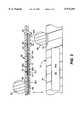
- FIG. 1is an exploded, perspective view of an interposer made according to the present invention, for assembly to an integrated circuit and a circuit panel;
- FIG. 2is a perspective bottom view of the interposer of FIG. 1;
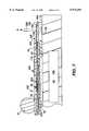
- FIG. 3is a greatly enlarged, exploded, cross-sectional, fragmentary, side elevational view of the interposer shown juxtaposed and in alignment with the integrated circuit, taken along line 3--3 of FIG. 1;
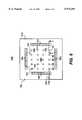
- FIG. 4is a diagrammatic, bottom plan topographic view of the interposer of FIGS. 1, 2 and 3, illustrating exemplary electrical interconnections between a plurality of contact pads and microelectronic units mounted within the interposer;
- FIG. 5is a flow chart illustrating the process of making the interposer of FIGS. 1 through 4;
- FIG. 6is a bottom plan view of another interposer according to the present invention.
- FIG. 7is a greatly enlarged cross-sectional, fragmentary, side elevational view of the interposer taken along line 7--7 of FIG. 6, shown atop an integrated circuit.
- FIGS. 1 and 3they illustrate an interposer (also referred to as a mounting component) 10 made according to the present invention, for assembly between an integrated circuit 12 and a circuit panel (also referred to as circuit board) 14.
- the integrated circuit 12is formed of silicon or similar other material used in the manufacture of integrated circuits.
- the circuit panel 14is made of ceramic material used in the formation of circuit panels.
- the interposer 10includes an upper insulation layer 16 that is preferably made of alumina or another similar insulating and encapsulating material, such as silicon dioxide.
- the expansion coefficient of the interposer 10sufficiently matches those of the integrated circuit 12 and the circuit panel 14, thus significantly minimizing stress caused by the differential thermal expansion and contraction of the various constituent materials over the intended operating range.
- the dimensions of the interposer 10vary with the overall design of the assembly comprised of the interposer 10, the integrated circuit 12 and the circuit panel 14.
- the interposer 10may however be as thin as a few mils.
- the interposer 10includes a plurality of upper contact pads arranged in a desired pattern on any part of the interposer upper surface 33. Only one upper contact pad 30 is shown in FIG. 3 for illustration purpose. A solder ball 37 is placed on each upper contact pad 30 (FIG. 3). FIG. 1 shows a pattern of solder balls 37, 39, 41, 43 that overlay corresponding upper pads 30. In certain embodiments it may be desirable to overlay only selected upper contact pads 30 with solder balls 37 whose pattern generally corresponds to the pattern of connections to micro-devices, such as semiconductor chips and discrete components 50, 52, 54 (FIG. 3) mounted within the interposer 10. While the present invention is described with respect to solder balls, it should be clear that alternative electrical connection techniques (or electrical connectors) may be used.
- the pattern of the upper contact pads 30corresponds to a matching pattern of contact pads (not shown) on the bottom surface of the circuit panel 14.
- the term “bottom”is interchangeable with the term “lower”.
- the interposer 10further includes a plurality of lower contact pads 60, 62, 64, 66, 68, 70 that are arranged in a desired pattern on any part of the bottom surface 73 of the interposer 10.
- the pattern of the lower contact pads 60, 62, 64, 66, 68, 70generally corresponds to a matching pattern of contact pads (only one of which 75, is illustrated in FIG. 3) on the upper surface 76 of the integrated circuit 12.
- These contact pads 75are overlaid with corresponding solder balls 80, 82, 84, 86, 88, 90 (FIG. 1), and their patten corresponds to the pattern of connections to micro-devices, such as semiconductor chips and discrete electronic components contained within a die 98, which is illustrated by a block.
- solder balls 80, 82, 84, 86, 88, 90 overlaying the contact pads on the upper surface 76 of the integrated circuit 12match the lower contact pads 60, 62, 64, 66, 68, 70 on the bottom surface 73 of the interposer 10.
- the solder balls 80, 82, 84, 86, 88, 90are melted by heating the interposer 10 and the integrated circuit 12. As the molten solder cools and hardens, it establishes a mechanical and electrical connection between the interposer 10 and the integrated circuit 12.
- the interposer 10is assembled to the integrated circuit 12 as described above.
- the interposer (10)--integrated circuit (12) unitmay be marketed separately for subsequent assembly to the circuit panel 14.
- the interposer 10is assembled to the circuit panel 14 as described above, and the interposer (10)--circuit panel (14) unit may be marketed separately for subsequent assembly to the integrated circuit 12.
- the interposer 10, the integrated circuit 12, and the circuit panel 14may be almost simultaneously assembled, robotically or manually.
- the upper contact pads 30 and the lower contact pads 60, 62, 64, 66, 68, 70are selectively interconnected by means of conductive wiring or traces 100, via the micro-devices 50, 52, 54 (FIG. 3) mounted within the interposer 10.
- the lower contact pad 70is electrically connected to the upper contact pad 30, via an internal conductive path containing the micro-device 50 (i.e., a resistor), the micro-device 52 (i.e., an inductor), and the micro-device 54 (i.e., a capacitor).
- the micro-device 50i.e., a resistor
- the micro-device 52i.e., an inductor
- the micro-device 54i.e., a capacitor
- the present inventionrealizes the unprecedented ability to reduce noise generated by the integrated circuit 12; to minimize external wiring between the integrated circuit 12 and the circuit panel 14; and to economically incorporate signal conditioning and inductive components within the interposer 10 that has approximately the same footprint as the integrated circuit 12.
- the various contact padsare made of conductive material, preferably gold traces. While only a few contact pads are illustrated, it should be clear that a significantly greater number of contact pads may be designed and used.
- the terms "top”, “bottom”, “upper”, and “lower”are used herein to indicate directions relative to the interposer 10 as shown in FIG. 1. It should be understood that the frame of reference is not necessarily to the ordinary, gravitational frame of reference.
- the interposer 10may be made using the processing methods described in U.S. Pat. No. 5,174,012 to Hamilton, which is incorporated herein by reference.
- the interposer 10is formed using wafer/thin film processing techniques.
- FIG. 5illustrates one such process 200, according to which the array of upper pads 30 are formed at step 202 by depositing gold traces on a thin etchable layer (not shown).
- the etchable layeris composed of a thin metallic film (for example copper) of approximately 1000 ⁇ (Angstroms) that is sputter or evaporation deposited on a wafer (not shows), which is electroplated to form an etchable layer of copper approximately 3 to 20 microns thick.
- the upper layer 16 of aluminais deposited (for instance by sputtering), on the etchable layer, at step 204.
- the upper layer 16is also referred to as the base encapsulant layer, and it provides mechanical strength to the interposer 10.
- the upper layer 16is lapped until it is planarized, and the upper pad array is exposed.
- a first yoke 209 of the inductor 52is formed using available photolithography and plating techniques.
- the first yoke 209is preferably formed of permalloy (NiFe).
- a first insulation layer 211 of the inductor 52is deposited on the first yoke 209, and a first inductive coil layer 212 is formed within the first insulation layer 211 (FIG. 3) at step 214.
- the coil layer 212is made of an electrically conductive material, preferably copper.
- one or more additional layers of inductive coil layers and insulation layersmay be similarly interposed on top, to reach the desired inductance, as illustrated by the exemplary steps 216, 218 and 220.
- an inductor gap layer 221composed for instance of alumina, is deposited on the uppermost insulation layer at step 222, and a second yoke 223 preferably formed of permalloy (NiFe), is deposited on the inductor gap layer 221 at step 224, which completes the formation of the inductor 52.
- the resistor (or a resistor array composed of a plurality of resistors) 50is formed at step 226 by depositing a thin film resistive layer.
- an electrically conductive trace 227extends from the coil 212, and is connected to the resistor 50, for connecting the inductor 52 to the resistor 50.
- the capacitor (or a capacitor array composed of a plurality of capacitors) 54is formed at step 228, by sequentially depositing a first conductive layer, followed by an insulation layer and a second conductive layer.
- Step 232is optional, and is relevant to the interposer 120 described below in connection with FIGS. 6 and 7. According to step 232, gold leads 188 form the central terminals 121, 123, 124, 125.
- a bottom insulation layer 233preferably made of alumina or another similar insulating and encapsulating material, such as silicon dioxide is formed. If some or all the lower contact pads 60, 62, 64, 66, 68, 70 were to be exposed, as is shown in FIG. 3 with regard to the interposer 10, vias or openings 235 are formed by selectively etching the bottom insulation layer 233 (step 236).
- the wafer on which the array of interposers 10 is formedis then immersed in an etchant solution for dissolving the etchable layer of copper, thus causing the array of interposers 10 to be released from the wafer (step 238).
- the etchant solutionis of a composition that selectively etches away copper.
- the individual interposers 10are then shipped for subsequent processing or packaging (step 240).
- the inductive micro-device 52may be an inductor, or a magnetic coil assembly as described in the U.S. patent application titled “Magnetic Coil Assembly", Ser. No. 08/844,003, which is incorporated herein by reference.
- the remaining micro-devices 50, 54may be formed using conventional thin-film techniques, including sputtering, photolithography, plating, or etching, prior to etching away the copper release layer.
- interposer 10provides an efficient match between ceramic-based circuit panels 14
- the interposer 120 shown in FIGS. 6 and 7provides an efficient match between plastic or polyimide-based circuit panels 14 having much greater differential thermal expansion and contraction.
- the interposer 120employs additional spring action to absorb excess expansion or contraction.
- the interposer 120is generally similar to the interposer 10, except that the interposer 120 uses a different method for electrically connecting the interposer 120 to the integrated circuit 12. Rather than using solder balls 80, 82, 84, 86, 88, 90 (FIG. 1), the interposer 120 includes a plurality of electrically conductive central terminals, i.e., 121, 123, 124, 125 that extend outwardly from the lower contact pads 60, 62, 64, 66, 68, 70. The interposer 120 may further include a plurality of peripheral terminals disposed in a desired pattern and extending inwardly from peripheral contact pads, i.e., 129. Only one peripheral terminal 127 is shown for the purpose of illustration. FIG.
- FIG. 7illustrates the formation of an electrical connection between the lower contact pad 70 of the interposer 120 and a contact pad 150 on (or embedded at least in part within) the integrated circuit 12, by breaking the terminal 125 at a frangible section 153, and forcing it downwardly in contact with the pad 150.
- the terminals 121, 123, 124, 125replace (or supplement) the solder balls 90.
- terminals 121, 123, 124, 125, 127are described as connecting the lower contact pads 60, 62, 64, 66, 68, 70 of the interposer 120, it should be clear that the terminals 121, 123, 124, 125, 127 may be used to interconnect the upper contact pads 30 to contact pads on the circuit panel 14.
- the interposer 120includes a plurality of generally similar elongated slots 160, 161, 162, 163, four of which are illustrated. Each slot, for example representative slot 163, extends through the interposer 120, from the top surface 170 to the bottom surface 173.
- the slots 160, 161, 162, 163divide the interposer 120 into an inner section 180 substantially bounded by the slots 160, 161, 162, 163, and an outer peripheral section 182 disposed outside of the slots 160, 161, 162, 163. While the slots 160, 161, 162, 163 are shown to be peripherally disposed relative to the interposer 120, it should be clear that these and other slots may be placed at any desired position across the surface of the interposer 120.
- central terminals 121, 123, 124, 125are disposed on the central section 180 and the peripheral terminals 127 are disposed on the peripheral section 182.
- FIG. 6depicts only a relatively small number of central and peripheral terminals. In actual practice, however, there may be a much greater number of terminals.
- Each central terminalfor example central terminal 125 (FIG. 7) includes a terminal lead 188 disposed between the upper surface 170 and the bottom surface 173 of the interposer 120, and extending across the associated slot 163.
- Each central terminal 125further includes a frangible section 153 that lies within the slot 163, and a peripheral end 190 secured within the peripheral section 182.
- the central terminal 125is forced into contact with the contact pad 150 of the integrated circuit 12 by means of a bonding tool 200 that exerts sufficient force on the central terminal 125 to break the lead 188 at the frangible section 153.
- the bonding tool 200then bonds the free end of the lead 188 to the contact pad 150 by means of available techniques, for instance ultra-sonically.
- the bonding tool 200is retracted and the bonding operation is repeated as needed to bond all the central and peripheral terminals.
- Each central terminal 125creates a spring action which absorbs excess contraction or expansion.
- connection and bonding methodsmay alternatively be selected, without affecting the scope of the present invention.
- Some of these methods and associated bonding toolsare described for example in U.S. Pat. Nos. 5,148,265; 5,148,266; 5,258,330; 5,282,312; 5,346,861; 5,347,159; 5,367,764; 5,390,844; 5,398,863; 5,414,298; 5,455,390; 5,477,611; 5,489,749; 5,491,302; 5,518,964; 5,525,545; and 5,536,909, all of which are incorporated herein by reference.
Landscapes
- Engineering & Computer Science (AREA)
- Microelectronics & Electronic Packaging (AREA)
- Physics & Mathematics (AREA)
- Condensed Matter Physics & Semiconductors (AREA)
- General Physics & Mathematics (AREA)
- Computer Hardware Design (AREA)
- Power Engineering (AREA)
- Structures For Mounting Electric Components On Printed Circuit Boards (AREA)
Abstract
Description
Claims (23)
Priority Applications (1)
| Application Number | Priority Date | Filing Date | Title |
|---|---|---|---|
| US08/989,326US5973391A (en) | 1997-12-11 | 1997-12-11 | Interposer with embedded circuitry and method for using the same to package microelectronic units |
Applications Claiming Priority (1)
| Application Number | Priority Date | Filing Date | Title |
|---|---|---|---|
| US08/989,326US5973391A (en) | 1997-12-11 | 1997-12-11 | Interposer with embedded circuitry and method for using the same to package microelectronic units |
Publications (1)
| Publication Number | Publication Date |
|---|---|
| US5973391Atrue US5973391A (en) | 1999-10-26 |
Family
ID=25535017
Family Applications (1)
| Application Number | Title | Priority Date | Filing Date |
|---|---|---|---|
| US08/989,326Expired - LifetimeUS5973391A (en) | 1997-12-11 | 1997-12-11 | Interposer with embedded circuitry and method for using the same to package microelectronic units |
Country Status (1)
| Country | Link |
|---|---|
| US (1) | US5973391A (en) |
Cited By (93)
| Publication number | Priority date | Publication date | Assignee | Title |
|---|---|---|---|---|
| US6180445B1 (en) | 2000-04-24 | 2001-01-30 | Taiwan Semiconductor Manufacturing Company | Method to fabricate high Q inductor by redistribution layer when flip-chip package is employed |
| US6303992B1 (en)* | 1999-07-06 | 2001-10-16 | Visteon Global Technologies, Inc. | Interposer for mounting semiconductor dice on substrates |
| US6335210B1 (en)* | 1999-12-17 | 2002-01-01 | International Business Machines Corporation | Baseplate for chip burn-in and/of testing, and method thereof |
| US6380629B1 (en)* | 1999-06-29 | 2002-04-30 | Hyundai Electronics Industries Co., Ltd. | Wafer level stack package and method of fabricating the same |
| US6486415B2 (en) | 2001-01-16 | 2002-11-26 | International Business Machines Corporation | Compliant layer for encapsulated columns |
| US6496355B1 (en) | 2001-10-04 | 2002-12-17 | Avx Corporation | Interdigitated capacitor with ball grid array (BGA) terminations |
| US20030225618A1 (en)* | 2002-05-28 | 2003-12-04 | Hessburg Matthew Benedict | System and method for exchanging loyalty points for acquisitions |
| US20040032011A1 (en)* | 2001-08-28 | 2004-02-19 | Tessera, Inc. | Microelectronic assemblies incorporating inductors |
| US6759316B2 (en)* | 1998-08-18 | 2004-07-06 | Oki Electric Industry Co., Ltd. | Method of manufacturing a semiconductor chip |
| US20040214372A1 (en)* | 2003-04-07 | 2004-10-28 | Walter Moden | Method for fabricating image sensor semiconductor package |
| US20040238857A1 (en)* | 2001-08-28 | 2004-12-02 | Tessera, Inc. | High frequency chip packages with connecting elements |
| US20050003171A1 (en)* | 2003-02-06 | 2005-01-06 | R-Tec Corporation | Plated via interposer |
| US20050017348A1 (en)* | 2003-02-25 | 2005-01-27 | Tessera, Inc. | Manufacture of mountable capped chips |
| US20050046041A1 (en)* | 2003-08-29 | 2005-03-03 | Advanced Semiconductor Engineering, Inc. | Integrated circuit device with embedded passive component by flip-chip connection and method for manufacturing the same |
| US20050173805A1 (en)* | 2003-12-30 | 2005-08-11 | Tessera, Inc. | Micro pin grid array with pin motion isolation |
| US20050181655A1 (en)* | 2003-12-30 | 2005-08-18 | Tessera, Inc. | Micro pin grid array with wiping action |
| US20050181544A1 (en)* | 2003-12-30 | 2005-08-18 | Tessera, Inc. | Microelectronic packages and methods therefor |
| US20050284658A1 (en)* | 2003-10-06 | 2005-12-29 | Tessera, Inc. | Components with posts and pads |
| WO2006004672A1 (en)* | 2004-06-25 | 2006-01-12 | Tessera, Inc. | Components with posts and pads |
| US20060024900A1 (en)* | 2004-07-29 | 2006-02-02 | Lee Teck K | Interposer including at least one passive element at least partially defined by a recess formed therein, method of manufacture, system including same, and wafer-scale interposer |
| EP1315207A3 (en)* | 2001-11-26 | 2006-09-20 | Matsushita Electric Industrial Co., Ltd. | Semiconductor module |
| US20060249857A1 (en)* | 2005-03-16 | 2006-11-09 | Tessera, Inc. | Microelectronic packages and methods therefor |
| US7224056B2 (en) | 2003-09-26 | 2007-05-29 | Tessera, Inc. | Back-face and edge interconnects for lidded package |
| US20070148822A1 (en)* | 2005-12-23 | 2007-06-28 | Tessera, Inc. | Microelectronic packages and methods therefor |
| US20070148819A1 (en)* | 2005-12-23 | 2007-06-28 | Tessera, Inc. | Microelectronic assemblies having very fine pitch stacking |
| US7265440B2 (en) | 2003-06-16 | 2007-09-04 | Tessera Technologies Hungary Kft. | Methods and apparatus for packaging integrated circuit devices |
| US20080003402A1 (en)* | 2003-10-06 | 2008-01-03 | Tessera, Inc. | Fine pitch microcontacts and method for forming thereof |
| US20080042273A1 (en)* | 1998-12-21 | 2008-02-21 | Megica Corporation | High performance system-on-chip using post passivation process |
| US20080233667A1 (en)* | 2003-12-31 | 2008-09-25 | Intel Corporation | Microdisplay packaging system |
| US20080296697A1 (en)* | 2007-05-29 | 2008-12-04 | Chao-Shun Hsu | Programmable semiconductor interposer for electronic package and method of forming |
| US7462936B2 (en) | 2003-10-06 | 2008-12-09 | Tessera, Inc. | Formation of circuitry with modification of feature height |
| US20090001511A1 (en)* | 2005-03-29 | 2009-01-01 | Megica Corporation | High performance system-on-chip using post passivation process |
| US7479398B2 (en) | 2003-07-03 | 2009-01-20 | Tessera Technologies Hungary Kft. | Methods and apparatus for packaging integrated circuit devices |
| US20090104736A1 (en)* | 2004-11-03 | 2009-04-23 | Tessera, Inc. | Stacked Packaging Improvements |
| US20100044860A1 (en)* | 2008-08-21 | 2010-02-25 | Tessera Interconnect Materials, Inc. | Microelectronic substrate or element having conductive pads and metal posts joined thereto using bond layer |
| US7936062B2 (en) | 2006-01-23 | 2011-05-03 | Tessera Technologies Ireland Limited | Wafer level chip packaging |
| US8143095B2 (en) | 2005-03-22 | 2012-03-27 | Tessera, Inc. | Sequential fabrication of vertical conductive interconnects in capped chips |
| CN101814485B (en)* | 2009-02-23 | 2012-08-22 | 万国半导体股份有限公司 | Packaging and fabricating method for mini power semiconductor with stacked inductance IC chip |
| US8330272B2 (en) | 2010-07-08 | 2012-12-11 | Tessera, Inc. | Microelectronic packages with dual or multiple-etched flip-chip connectors |
| US8404520B1 (en) | 2011-10-17 | 2013-03-26 | Invensas Corporation | Package-on-package assembly with wire bond vias |
| US8482111B2 (en) | 2010-07-19 | 2013-07-09 | Tessera, Inc. | Stackable molded microelectronic packages |
| US8580607B2 (en) | 2010-07-27 | 2013-11-12 | Tessera, Inc. | Microelectronic packages with nanoparticle joining |
| US8604605B2 (en) | 2007-01-05 | 2013-12-10 | Invensas Corp. | Microelectronic assembly with multi-layer support structure |
| US8623706B2 (en) | 2010-11-15 | 2014-01-07 | Tessera, Inc. | Microelectronic package with terminals on dielectric mass |
| US8835228B2 (en) | 2012-05-22 | 2014-09-16 | Invensas Corporation | Substrate-less stackable package with wire-bond interconnect |
| US8853558B2 (en) | 2010-12-10 | 2014-10-07 | Tessera, Inc. | Interconnect structure |
| US8872318B2 (en) | 2011-08-24 | 2014-10-28 | Tessera, Inc. | Through interposer wire bond using low CTE interposer with coarse slot apertures |
| US8878353B2 (en) | 2012-12-20 | 2014-11-04 | Invensas Corporation | Structure for microelectronic packaging with bond elements to encapsulation surface |
| US8883563B1 (en) | 2013-07-15 | 2014-11-11 | Invensas Corporation | Fabrication of microelectronic assemblies having stack terminals coupled by connectors extending through encapsulation |
| US8884448B2 (en) | 2007-09-28 | 2014-11-11 | Tessera, Inc. | Flip chip interconnection with double post |
| US8975738B2 (en) | 2012-11-12 | 2015-03-10 | Invensas Corporation | Structure for microelectronic packaging with terminals on dielectric mass |
| US9023691B2 (en) | 2013-07-15 | 2015-05-05 | Invensas Corporation | Microelectronic assemblies with stack terminals coupled by connectors extending through encapsulation |
| US9034696B2 (en) | 2013-07-15 | 2015-05-19 | Invensas Corporation | Microelectronic assemblies having reinforcing collars on connectors extending through encapsulation |
| US9082753B2 (en) | 2013-11-12 | 2015-07-14 | Invensas Corporation | Severing bond wire by kinking and twisting |
| US9087815B2 (en) | 2013-11-12 | 2015-07-21 | Invensas Corporation | Off substrate kinking of bond wire |
| US9093435B2 (en) | 2011-05-03 | 2015-07-28 | Tessera, Inc. | Package-on-package assembly with wire bonds to encapsulation surface |
| US9159708B2 (en) | 2010-07-19 | 2015-10-13 | Tessera, Inc. | Stackable molded microelectronic packages with area array unit connectors |
| US9214454B2 (en) | 2014-03-31 | 2015-12-15 | Invensas Corporation | Batch process fabrication of package-on-package microelectronic assemblies |
| US9224717B2 (en) | 2011-05-03 | 2015-12-29 | Tessera, Inc. | Package-on-package assembly with wire bonds to encapsulation surface |
| US9324681B2 (en) | 2010-12-13 | 2016-04-26 | Tessera, Inc. | Pin attachment |
| US9349706B2 (en) | 2012-02-24 | 2016-05-24 | Invensas Corporation | Method for package-on-package assembly with wire bonds to encapsulation surface |
| US9391008B2 (en) | 2012-07-31 | 2016-07-12 | Invensas Corporation | Reconstituted wafer-level package DRAM |
| US9412714B2 (en) | 2014-05-30 | 2016-08-09 | Invensas Corporation | Wire bond support structure and microelectronic package including wire bonds therefrom |
| US9502390B2 (en) | 2012-08-03 | 2016-11-22 | Invensas Corporation | BVA interposer |
| US9583411B2 (en) | 2014-01-17 | 2017-02-28 | Invensas Corporation | Fine pitch BVA using reconstituted wafer with area array accessible for testing |
| US9601454B2 (en) | 2013-02-01 | 2017-03-21 | Invensas Corporation | Method of forming a component having wire bonds and a stiffening layer |
| US9633971B2 (en) | 2015-07-10 | 2017-04-25 | Invensas Corporation | Structures and methods for low temperature bonding using nanoparticles |
| US9646917B2 (en) | 2014-05-29 | 2017-05-09 | Invensas Corporation | Low CTE component with wire bond interconnects |
| US9659848B1 (en) | 2015-11-18 | 2017-05-23 | Invensas Corporation | Stiffened wires for offset BVA |
| US9685365B2 (en) | 2013-08-08 | 2017-06-20 | Invensas Corporation | Method of forming a wire bond having a free end |
| US9691679B2 (en) | 2012-02-24 | 2017-06-27 | Invensas Corporation | Method for package-on-package assembly with wire bonds to encapsulation surface |
| US9728527B2 (en) | 2013-11-22 | 2017-08-08 | Invensas Corporation | Multiple bond via arrays of different wire heights on a same substrate |
| US9735084B2 (en) | 2014-12-11 | 2017-08-15 | Invensas Corporation | Bond via array for thermal conductivity |
| US9761554B2 (en) | 2015-05-07 | 2017-09-12 | Invensas Corporation | Ball bonding metal wire bond wires to metal pads |
| US9812402B2 (en) | 2015-10-12 | 2017-11-07 | Invensas Corporation | Wire bond wires for interference shielding |
| US9842745B2 (en) | 2012-02-17 | 2017-12-12 | Invensas Corporation | Heat spreading substrate with embedded interconnects |
| US9852969B2 (en) | 2013-11-22 | 2017-12-26 | Invensas Corporation | Die stacks with one or more bond via arrays of wire bond wires and with one or more arrays of bump interconnects |
| US9888579B2 (en) | 2015-03-05 | 2018-02-06 | Invensas Corporation | Pressing of wire bond wire tips to provide bent-over tips |
| US9911718B2 (en) | 2015-11-17 | 2018-03-06 | Invensas Corporation | ‘RDL-First’ packaged microelectronic device for a package-on-package device |
| US9935075B2 (en) | 2016-07-29 | 2018-04-03 | Invensas Corporation | Wire bonding method and apparatus for electromagnetic interference shielding |
| US9984992B2 (en) | 2015-12-30 | 2018-05-29 | Invensas Corporation | Embedded wire bond wires for vertical integration with separate surface mount and wire bond mounting surfaces |
| US10008469B2 (en) | 2015-04-30 | 2018-06-26 | Invensas Corporation | Wafer-level packaging using wire bond wires in place of a redistribution layer |
| US10008477B2 (en) | 2013-09-16 | 2018-06-26 | Invensas Corporation | Microelectronic element with bond elements to encapsulation surface |
| US10026717B2 (en) | 2013-11-22 | 2018-07-17 | Invensas Corporation | Multiple bond via arrays of different wire heights on a same substrate |
| US10181457B2 (en) | 2015-10-26 | 2019-01-15 | Invensas Corporation | Microelectronic package for wafer-level chip scale packaging with fan-out |
| US10299368B2 (en) | 2016-12-21 | 2019-05-21 | Invensas Corporation | Surface integrated waveguides and circuit structures therefor |
| US10332854B2 (en) | 2015-10-23 | 2019-06-25 | Invensas Corporation | Anchoring structure of fine pitch bva |
| US10381326B2 (en) | 2014-05-28 | 2019-08-13 | Invensas Corporation | Structure and method for integrated circuits packaging with increased density |
| US10460958B2 (en) | 2013-08-07 | 2019-10-29 | Invensas Corporation | Method of manufacturing embedded packaging with preformed vias |
| US10490528B2 (en) | 2015-10-12 | 2019-11-26 | Invensas Corporation | Embedded wire bond wires |
| US10535626B2 (en) | 2015-07-10 | 2020-01-14 | Invensas Corporation | Structures and methods for low temperature bonding using nanoparticles |
| US11973056B2 (en) | 2016-10-27 | 2024-04-30 | Adeia Semiconductor Technologies Llc | Methods for low temperature bonding using nanoparticles |
| US12211809B2 (en) | 2020-12-30 | 2025-01-28 | Adeia Semiconductor Bonding Technologies Inc. | Structure with conductive feature and method of forming same |
Citations (24)
| Publication number | Priority date | Publication date | Assignee | Title |
|---|---|---|---|---|
| US4349862A (en)* | 1980-08-11 | 1982-09-14 | International Business Machines Corporation | Capacitive chip carrier and multilayer ceramic capacitors |
| US4617730A (en)* | 1984-08-13 | 1986-10-21 | International Business Machines Corporation | Method of fabricating a chip interposer |
| US4782381A (en)* | 1987-06-12 | 1988-11-01 | Hewlett-Packard Company | Chip carrier |
| US4939568A (en)* | 1986-03-20 | 1990-07-03 | Fujitsu Limited | Three-dimensional integrated circuit and manufacturing method thereof |
| US5070317A (en)* | 1989-01-17 | 1991-12-03 | Bhagat Jayant K | Miniature inductor for integrated circuits and devices |
| US5148266A (en)* | 1990-09-24 | 1992-09-15 | Ist Associates, Inc. | Semiconductor chip assemblies having interposer and flexible lead |
| US5148265A (en)* | 1990-09-24 | 1992-09-15 | Ist Associates, Inc. | Semiconductor chip assemblies with fan-in leads |
| US5174012A (en)* | 1989-11-27 | 1992-12-29 | Censtor Corp. | Method of making magnetic read/write head/flexure/conductor unit(s) |
| US5177594A (en)* | 1991-01-09 | 1993-01-05 | International Business Machines Corporation | Semiconductor chip interposer module with engineering change wiring and distributed decoupling capacitance |
| US5258330A (en)* | 1990-09-24 | 1993-11-02 | Tessera, Inc. | Semiconductor chip assemblies with fan-in leads |
| US5282312A (en)* | 1991-12-31 | 1994-02-01 | Tessera, Inc. | Multi-layer circuit construction methods with customization features |
| US5367764A (en)* | 1991-12-31 | 1994-11-29 | Tessera, Inc. | Method of making a multi-layer circuit assembly |
| US5382827A (en)* | 1992-08-07 | 1995-01-17 | Fujitsu Limited | Functional substrates for packaging semiconductor chips |
| US5390844A (en)* | 1993-07-23 | 1995-02-21 | Tessera, Inc. | Semiconductor inner lead bonding tool |
| US5398863A (en)* | 1993-07-23 | 1995-03-21 | Tessera, Inc. | Shaped lead structure and method |
| US5404044A (en)* | 1992-09-29 | 1995-04-04 | International Business Machines Corporation | Parallel process interposer (PPI) |
| US5414298A (en)* | 1993-03-26 | 1995-05-09 | Tessera, Inc. | Semiconductor chip assemblies and components with pressure contact |
| US5426072A (en)* | 1993-01-21 | 1995-06-20 | Hughes Aircraft Company | Process of manufacturing a three dimensional integrated circuit from stacked SOI wafers using a temporary silicon substrate |
| US5455390A (en)* | 1994-02-01 | 1995-10-03 | Tessera, Inc. | Microelectronics unit mounting with multiple lead bonding |
| US5477611A (en)* | 1993-09-20 | 1995-12-26 | Tessera, Inc. | Method of forming interface between die and chip carrier |
| US5489749A (en)* | 1992-07-24 | 1996-02-06 | Tessera, Inc. | Semiconductor connection components and method with releasable lead support |
| US5491302A (en)* | 1994-09-19 | 1996-02-13 | Tessera, Inc. | Microelectronic bonding with lead motion |
| US5518964A (en)* | 1994-07-07 | 1996-05-21 | Tessera, Inc. | Microelectronic mounting with multiple lead deformation and bonding |
| US5783870A (en)* | 1995-03-16 | 1998-07-21 | National Semiconductor Corporation | Method for connecting packages of a stacked ball grid array structure |
- 1997
- 1997-12-11USUS08/989,326patent/US5973391A/ennot_activeExpired - Lifetime
Patent Citations (28)
| Publication number | Priority date | Publication date | Assignee | Title |
|---|---|---|---|---|
| US4349862A (en)* | 1980-08-11 | 1982-09-14 | International Business Machines Corporation | Capacitive chip carrier and multilayer ceramic capacitors |
| US4617730A (en)* | 1984-08-13 | 1986-10-21 | International Business Machines Corporation | Method of fabricating a chip interposer |
| US4939568A (en)* | 1986-03-20 | 1990-07-03 | Fujitsu Limited | Three-dimensional integrated circuit and manufacturing method thereof |
| US4782381A (en)* | 1987-06-12 | 1988-11-01 | Hewlett-Packard Company | Chip carrier |
| US5070317A (en)* | 1989-01-17 | 1991-12-03 | Bhagat Jayant K | Miniature inductor for integrated circuits and devices |
| US5174012A (en)* | 1989-11-27 | 1992-12-29 | Censtor Corp. | Method of making magnetic read/write head/flexure/conductor unit(s) |
| US5347159A (en)* | 1990-09-24 | 1994-09-13 | Tessera, Inc. | Semiconductor chip assemblies with face-up mounting and rear-surface connection to substrate |
| US5148265A (en)* | 1990-09-24 | 1992-09-15 | Ist Associates, Inc. | Semiconductor chip assemblies with fan-in leads |
| US5258330A (en)* | 1990-09-24 | 1993-11-02 | Tessera, Inc. | Semiconductor chip assemblies with fan-in leads |
| US5346861A (en)* | 1990-09-24 | 1994-09-13 | Tessera, Inc. | Semiconductor chip assemblies and methods of making same |
| US5148266A (en)* | 1990-09-24 | 1992-09-15 | Ist Associates, Inc. | Semiconductor chip assemblies having interposer and flexible lead |
| US5177594A (en)* | 1991-01-09 | 1993-01-05 | International Business Machines Corporation | Semiconductor chip interposer module with engineering change wiring and distributed decoupling capacitance |
| US5282312A (en)* | 1991-12-31 | 1994-02-01 | Tessera, Inc. | Multi-layer circuit construction methods with customization features |
| US5367764A (en)* | 1991-12-31 | 1994-11-29 | Tessera, Inc. | Method of making a multi-layer circuit assembly |
| US5489749A (en)* | 1992-07-24 | 1996-02-06 | Tessera, Inc. | Semiconductor connection components and method with releasable lead support |
| US5536909A (en)* | 1992-07-24 | 1996-07-16 | Tessera, Inc. | Semiconductor connection components and methods with releasable lead support |
| US5382827A (en)* | 1992-08-07 | 1995-01-17 | Fujitsu Limited | Functional substrates for packaging semiconductor chips |
| US5404044A (en)* | 1992-09-29 | 1995-04-04 | International Business Machines Corporation | Parallel process interposer (PPI) |
| US5426072A (en)* | 1993-01-21 | 1995-06-20 | Hughes Aircraft Company | Process of manufacturing a three dimensional integrated circuit from stacked SOI wafers using a temporary silicon substrate |
| US5414298A (en)* | 1993-03-26 | 1995-05-09 | Tessera, Inc. | Semiconductor chip assemblies and components with pressure contact |
| US5525545A (en)* | 1993-03-26 | 1996-06-11 | Tessera, Inc. | Semiconductor chip assemblies and components with pressure contact |
| US5398863A (en)* | 1993-07-23 | 1995-03-21 | Tessera, Inc. | Shaped lead structure and method |
| US5390844A (en)* | 1993-07-23 | 1995-02-21 | Tessera, Inc. | Semiconductor inner lead bonding tool |
| US5477611A (en)* | 1993-09-20 | 1995-12-26 | Tessera, Inc. | Method of forming interface between die and chip carrier |
| US5455390A (en)* | 1994-02-01 | 1995-10-03 | Tessera, Inc. | Microelectronics unit mounting with multiple lead bonding |
| US5518964A (en)* | 1994-07-07 | 1996-05-21 | Tessera, Inc. | Microelectronic mounting with multiple lead deformation and bonding |
| US5491302A (en)* | 1994-09-19 | 1996-02-13 | Tessera, Inc. | Microelectronic bonding with lead motion |
| US5783870A (en)* | 1995-03-16 | 1998-07-21 | National Semiconductor Corporation | Method for connecting packages of a stacked ball grid array structure |
Non-Patent Citations (4)
| Title |
|---|
| Levine, B. "Chip-Scale, Bare Die Face Challenges", Electronic News Article, vol. 43, No. 2149, Monday, Jan. 6, 1997. |
| Levine, B. Chip Scale, Bare Die Face Challenges , Electronic News Article, vol. 43, No. 2149, Monday, Jan. 6, 1997.* |
| Shell Case Marketing and Technical Literature, "True Miniature Die Size IC Packaging Solution". |
| Shell Case Marketing and Technical Literature, True Miniature Die Size IC Packaging Solution .* |
Cited By (217)
| Publication number | Priority date | Publication date | Assignee | Title |
|---|---|---|---|---|
| US6759316B2 (en)* | 1998-08-18 | 2004-07-06 | Oki Electric Industry Co., Ltd. | Method of manufacturing a semiconductor chip |
| US20080042239A1 (en)* | 1998-12-21 | 2008-02-21 | Megica Corporation | High performance system-on-chip using post passivation process |
| US20080044977A1 (en)* | 1998-12-21 | 2008-02-21 | Megica Corporation | High performance system-on-chip using post passivation process |
| US8487400B2 (en) | 1998-12-21 | 2013-07-16 | Megica Corporation | High performance system-on-chip using post passivation process |
| US20080093745A1 (en)* | 1998-12-21 | 2008-04-24 | Megica Corporation | High performance system-on-chip using post passivation process |
| US20080042273A1 (en)* | 1998-12-21 | 2008-02-21 | Megica Corporation | High performance system-on-chip using post passivation process |
| US6380629B1 (en)* | 1999-06-29 | 2002-04-30 | Hyundai Electronics Industries Co., Ltd. | Wafer level stack package and method of fabricating the same |
| US6303992B1 (en)* | 1999-07-06 | 2001-10-16 | Visteon Global Technologies, Inc. | Interposer for mounting semiconductor dice on substrates |
| US6335210B1 (en)* | 1999-12-17 | 2002-01-01 | International Business Machines Corporation | Baseplate for chip burn-in and/of testing, and method thereof |
| US6180445B1 (en) | 2000-04-24 | 2001-01-30 | Taiwan Semiconductor Manufacturing Company | Method to fabricate high Q inductor by redistribution layer when flip-chip package is employed |
| US6486415B2 (en) | 2001-01-16 | 2002-11-26 | International Business Machines Corporation | Compliant layer for encapsulated columns |
| US7278207B2 (en) | 2001-01-16 | 2007-10-09 | International Business Machines Corporation | Method of making an electronic package |
| US20070278654A1 (en)* | 2001-01-16 | 2007-12-06 | Jimarez Lisa J | Method of making an electronic package |
| US20050250249A1 (en)* | 2001-01-16 | 2005-11-10 | Jimarez Lisa J | Method of making an electronic package |
| US6961995B2 (en) | 2001-01-16 | 2005-11-08 | International Business Machines Corporation | Method of making an electronic package |
| US20030020150A1 (en)* | 2001-01-16 | 2003-01-30 | International Business Machines Corporation | Compliant layer for encapsulated columns |
| US20040238934A1 (en)* | 2001-08-28 | 2004-12-02 | Tessera, Inc. | High-frequency chip packages |
| US7012323B2 (en) | 2001-08-28 | 2006-03-14 | Tessera, Inc. | Microelectronic assemblies incorporating inductors |
| US7268426B2 (en) | 2001-08-28 | 2007-09-11 | Tessera, Inc. | High-frequency chip packages |
| US7176506B2 (en) | 2001-08-28 | 2007-02-13 | Tessera, Inc. | High frequency chip packages with connecting elements |
| US20040032011A1 (en)* | 2001-08-28 | 2004-02-19 | Tessera, Inc. | Microelectronic assemblies incorporating inductors |
| US7566955B2 (en) | 2001-08-28 | 2009-07-28 | Tessera, Inc. | High-frequency chip packages |
| US6856007B2 (en) | 2001-08-28 | 2005-02-15 | Tessera, Inc. | High-frequency chip packages |
| US20040238857A1 (en)* | 2001-08-28 | 2004-12-02 | Tessera, Inc. | High frequency chip packages with connecting elements |
| US20060113645A1 (en)* | 2001-08-28 | 2006-06-01 | Tessera, Inc. | Microelectronic assemblies incorporating inductors |
| US6496355B1 (en) | 2001-10-04 | 2002-12-17 | Avx Corporation | Interdigitated capacitor with ball grid array (BGA) terminations |
| EP1315207A3 (en)* | 2001-11-26 | 2006-09-20 | Matsushita Electric Industrial Co., Ltd. | Semiconductor module |
| US7686218B2 (en) | 2002-05-28 | 2010-03-30 | American Express Travel Related Services Company, Inc. | System and method for exchanging loyalty points for acquisitions |
| US7680688B2 (en)* | 2002-05-28 | 2010-03-16 | American Express Travel Related Services Company, Inc. | System and method for exchanging loyalty points for acquisitions |
| US20030225618A1 (en)* | 2002-05-28 | 2003-12-04 | Hessburg Matthew Benedict | System and method for exchanging loyalty points for acquisitions |
| US20080021784A1 (en)* | 2002-05-28 | 2008-01-24 | American Express Travel Related Services Co., Inc. | System and method for exchanging loyalty points for acquisitions |
| US7828206B2 (en) | 2002-05-28 | 2010-11-09 | American Express Travel Related Services Company, Inc. | System and method for exchanging loyalty points for acquisitions |
| US20110015955A1 (en)* | 2002-05-28 | 2011-01-20 | American Express Travel Related Services Company, Inc. | System and method for exchanging loyalty points for acquisitions |
| US20080021785A1 (en)* | 2002-05-28 | 2008-01-24 | American Express Travel Related Services Co., Inc. | System and method for exchanging loyalty points for acquisitions |
| US20050003171A1 (en)* | 2003-02-06 | 2005-01-06 | R-Tec Corporation | Plated via interposer |
| US7754537B2 (en) | 2003-02-25 | 2010-07-13 | Tessera, Inc. | Manufacture of mountable capped chips |
| US20050017348A1 (en)* | 2003-02-25 | 2005-01-27 | Tessera, Inc. | Manufacture of mountable capped chips |
| US20040214372A1 (en)* | 2003-04-07 | 2004-10-28 | Walter Moden | Method for fabricating image sensor semiconductor package |
| US7215015B2 (en) | 2003-04-07 | 2007-05-08 | Micron Technology, Inc. | Imaging system |
| US6969632B2 (en) | 2003-04-07 | 2005-11-29 | Micron Technology, Inc. | Method for fabricating image sensor semiconductor package |
| US20050003579A1 (en)* | 2003-04-07 | 2005-01-06 | Walter Moden | Imaging system |
| US7265440B2 (en) | 2003-06-16 | 2007-09-04 | Tessera Technologies Hungary Kft. | Methods and apparatus for packaging integrated circuit devices |
| US7642629B2 (en) | 2003-06-16 | 2010-01-05 | Tessera Technologies Hungary Kft. | Methods and apparatus for packaging integrated circuit devices |
| US7479398B2 (en) | 2003-07-03 | 2009-01-20 | Tessera Technologies Hungary Kft. | Methods and apparatus for packaging integrated circuit devices |
| US7495341B2 (en) | 2003-07-03 | 2009-02-24 | Tessera Technologies Hungary Kft. | Methods and apparatus for packaging integrated circuit devices |
| US7670876B2 (en) | 2003-08-29 | 2010-03-02 | Advanced Semiconductor Engineering, Inc. | Integrated circuit device with embedded passive component by flip-chip connection and method for manufacturing the same |
| US20080233676A1 (en)* | 2003-08-29 | 2008-09-25 | Advanced Semiconductor Engineering, Inc. | Integrated circuit device with embedded passive component by flip-chip connection and method for manfacturing the same |
| US20050046041A1 (en)* | 2003-08-29 | 2005-03-03 | Advanced Semiconductor Engineering, Inc. | Integrated circuit device with embedded passive component by flip-chip connection and method for manufacturing the same |
| US7391118B2 (en)* | 2003-08-29 | 2008-06-24 | Advanced Semiconductor Engineering, Inc. | Integrated circuit device with embedded passive component by flip-chip connection and method for manufacturing the same |
| US7224056B2 (en) | 2003-09-26 | 2007-05-29 | Tessera, Inc. | Back-face and edge interconnects for lidded package |
| US20090133254A1 (en)* | 2003-10-06 | 2009-05-28 | Tessera, Inc. | Components with posts and pads |
| US20080003402A1 (en)* | 2003-10-06 | 2008-01-03 | Tessera, Inc. | Fine pitch microcontacts and method for forming thereof |
| US8641913B2 (en) | 2003-10-06 | 2014-02-04 | Tessera, Inc. | Fine pitch microcontacts and method for forming thereof |
| US7462936B2 (en) | 2003-10-06 | 2008-12-09 | Tessera, Inc. | Formation of circuitry with modification of feature height |
| US8604348B2 (en) | 2003-10-06 | 2013-12-10 | Tessera, Inc. | Method of making a connection component with posts and pads |
| US7816251B2 (en) | 2003-10-06 | 2010-10-19 | Tessera, Inc. | Formation of circuitry with modification of feature height |
| US8046912B2 (en) | 2003-10-06 | 2011-11-01 | Tessera, Inc. | Method of making a connection component with posts and pads |
| US7495179B2 (en) | 2003-10-06 | 2009-02-24 | Tessera, Inc. | Components with posts and pads |
| US20050284658A1 (en)* | 2003-10-06 | 2005-12-29 | Tessera, Inc. | Components with posts and pads |
| US7709968B2 (en) | 2003-12-30 | 2010-05-04 | Tessera, Inc. | Micro pin grid array with pin motion isolation |
| US7554206B2 (en) | 2003-12-30 | 2009-06-30 | Tessera, Inc. | Microelectronic packages and methods therefor |
| US20050173805A1 (en)* | 2003-12-30 | 2005-08-11 | Tessera, Inc. | Micro pin grid array with pin motion isolation |
| US20050181655A1 (en)* | 2003-12-30 | 2005-08-18 | Tessera, Inc. | Micro pin grid array with wiping action |
| US8531039B2 (en) | 2003-12-30 | 2013-09-10 | Tessera, Inc. | Micro pin grid array with pin motion isolation |
| US8207604B2 (en) | 2003-12-30 | 2012-06-26 | Tessera, Inc. | Microelectronic package comprising offset conductive posts on compliant layer |
| US20050181544A1 (en)* | 2003-12-30 | 2005-08-18 | Tessera, Inc. | Microelectronic packages and methods therefor |
| US7176043B2 (en) | 2003-12-30 | 2007-02-13 | Tessera, Inc. | Microelectronic packages and methods therefor |
| US20100193970A1 (en)* | 2003-12-30 | 2010-08-05 | Tessera, Inc. | Micro pin grid array with pin motion isolation |
| US8680572B2 (en) | 2003-12-31 | 2014-03-25 | Intel Corporation | Microdisplay packaging system |
| US8044431B2 (en)* | 2003-12-31 | 2011-10-25 | Intel Corporation | Microdisplay packaging system |
| US20080233667A1 (en)* | 2003-12-31 | 2008-09-25 | Intel Corporation | Microdisplay packaging system |
| WO2006004672A1 (en)* | 2004-06-25 | 2006-01-12 | Tessera, Inc. | Components with posts and pads |
| US7663206B2 (en) | 2004-07-29 | 2010-02-16 | Micron Tachnology, Inc. | Interposer including at least one passive element at least partially defined by a recess formed therein, system including same, and wafer-scale interposer |
| US7494889B2 (en)* | 2004-07-29 | 2009-02-24 | Micron Technology, Inc. | Method of manufacturing an interposer including at least one passive element at least partially defined by a recess therein |
| US20060024900A1 (en)* | 2004-07-29 | 2006-02-02 | Lee Teck K | Interposer including at least one passive element at least partially defined by a recess formed therein, method of manufacture, system including same, and wafer-scale interposer |
| US20060125047A1 (en)* | 2004-07-29 | 2006-06-15 | Lee Teck K | Interposer including at least one passive element at least partially defined by a recess formed therein, system including same, and wafer-scale interposer |
| US20110042810A1 (en)* | 2004-11-03 | 2011-02-24 | Tessera, Inc. | Stacked packaging improvements |
| US9153562B2 (en) | 2004-11-03 | 2015-10-06 | Tessera, Inc. | Stacked packaging improvements |
| US8927337B2 (en) | 2004-11-03 | 2015-01-06 | Tessera, Inc. | Stacked packaging improvements |
| US8531020B2 (en) | 2004-11-03 | 2013-09-10 | Tessera, Inc. | Stacked packaging improvements |
| US20090104736A1 (en)* | 2004-11-03 | 2009-04-23 | Tessera, Inc. | Stacked Packaging Improvements |
| US8525314B2 (en) | 2004-11-03 | 2013-09-03 | Tessera, Inc. | Stacked packaging improvements |
| US9570416B2 (en) | 2004-11-03 | 2017-02-14 | Tessera, Inc. | Stacked packaging improvements |
| US7939934B2 (en) | 2005-03-16 | 2011-05-10 | Tessera, Inc. | Microelectronic packages and methods therefor |
| US20060249857A1 (en)* | 2005-03-16 | 2006-11-09 | Tessera, Inc. | Microelectronic packages and methods therefor |
| US8143095B2 (en) | 2005-03-22 | 2012-03-27 | Tessera, Inc. | Sequential fabrication of vertical conductive interconnects in capped chips |
| US20090001511A1 (en)* | 2005-03-29 | 2009-01-01 | Megica Corporation | High performance system-on-chip using post passivation process |
| US8384189B2 (en) | 2005-03-29 | 2013-02-26 | Megica Corporation | High performance system-on-chip using post passivation process |
| US8093697B2 (en) | 2005-12-23 | 2012-01-10 | Tessera, Inc. | Microelectronic packages and methods therefor |
| US20110165733A1 (en)* | 2005-12-23 | 2011-07-07 | Tessera, Inc. | Microelectronic packages and methods therefor |
| US20070148819A1 (en)* | 2005-12-23 | 2007-06-28 | Tessera, Inc. | Microelectronic assemblies having very fine pitch stacking |
| US20070148822A1 (en)* | 2005-12-23 | 2007-06-28 | Tessera, Inc. | Microelectronic packages and methods therefor |
| US9218988B2 (en) | 2005-12-23 | 2015-12-22 | Tessera, Inc. | Microelectronic packages and methods therefor |
| US8728865B2 (en) | 2005-12-23 | 2014-05-20 | Tessera, Inc. | Microelectronic packages and methods therefor |
| US8067267B2 (en) | 2005-12-23 | 2011-11-29 | Tessera, Inc. | Microelectronic assemblies having very fine pitch stacking |
| US8058101B2 (en) | 2005-12-23 | 2011-11-15 | Tessera, Inc. | Microelectronic packages and methods therefor |
| US20100232129A1 (en)* | 2005-12-23 | 2010-09-16 | Tessera, Inc. | Microelectronic packages and methods therefor |
| US9984901B2 (en) | 2005-12-23 | 2018-05-29 | Tessera, Inc. | Method for making a microelectronic assembly having conductive elements |
| US7936062B2 (en) | 2006-01-23 | 2011-05-03 | Tessera Technologies Ireland Limited | Wafer level chip packaging |
| US8604605B2 (en) | 2007-01-05 | 2013-12-10 | Invensas Corp. | Microelectronic assembly with multi-layer support structure |
| US9548145B2 (en) | 2007-01-05 | 2017-01-17 | Invensas Corporation | Microelectronic assembly with multi-layer support structure |
| US8945998B2 (en) | 2007-05-29 | 2015-02-03 | Taiwan Semiconductor Manufacturing Company, Ltd. | Programmable semiconductor interposer for electronic package and method of forming |
| US20080296697A1 (en)* | 2007-05-29 | 2008-12-04 | Chao-Shun Hsu | Programmable semiconductor interposer for electronic package and method of forming |
| US8476735B2 (en)* | 2007-05-29 | 2013-07-02 | Taiwan Semiconductor Manufacturing Company, Ltd. | Programmable semiconductor interposer for electronic package and method of forming |
| US8884448B2 (en) | 2007-09-28 | 2014-11-11 | Tessera, Inc. | Flip chip interconnection with double post |
| US20100044860A1 (en)* | 2008-08-21 | 2010-02-25 | Tessera Interconnect Materials, Inc. | Microelectronic substrate or element having conductive pads and metal posts joined thereto using bond layer |
| CN101814485B (en)* | 2009-02-23 | 2012-08-22 | 万国半导体股份有限公司 | Packaging and fabricating method for mini power semiconductor with stacked inductance IC chip |
| US8330272B2 (en) | 2010-07-08 | 2012-12-11 | Tessera, Inc. | Microelectronic packages with dual or multiple-etched flip-chip connectors |
| US8723318B2 (en) | 2010-07-08 | 2014-05-13 | Tessera, Inc. | Microelectronic packages with dual or multiple-etched flip-chip connectors |
| US10128216B2 (en) | 2010-07-19 | 2018-11-13 | Tessera, Inc. | Stackable molded microelectronic packages |
| US9159708B2 (en) | 2010-07-19 | 2015-10-13 | Tessera, Inc. | Stackable molded microelectronic packages with area array unit connectors |
| US9553076B2 (en) | 2010-07-19 | 2017-01-24 | Tessera, Inc. | Stackable molded microelectronic packages with area array unit connectors |
| US9123664B2 (en) | 2010-07-19 | 2015-09-01 | Tessera, Inc. | Stackable molded microelectronic packages |
| US8907466B2 (en) | 2010-07-19 | 2014-12-09 | Tessera, Inc. | Stackable molded microelectronic packages |
| US9570382B2 (en) | 2010-07-19 | 2017-02-14 | Tessera, Inc. | Stackable molded microelectronic packages |
| US8482111B2 (en) | 2010-07-19 | 2013-07-09 | Tessera, Inc. | Stackable molded microelectronic packages |
| US9397063B2 (en) | 2010-07-27 | 2016-07-19 | Tessera, Inc. | Microelectronic packages with nanoparticle joining |
| US9030001B2 (en) | 2010-07-27 | 2015-05-12 | Tessera, Inc. | Microelectronic packages with nanoparticle joining |
| US8580607B2 (en) | 2010-07-27 | 2013-11-12 | Tessera, Inc. | Microelectronic packages with nanoparticle joining |
| US8659164B2 (en) | 2010-11-15 | 2014-02-25 | Tessera, Inc. | Microelectronic package with terminals on dielectric mass |
| US8957527B2 (en) | 2010-11-15 | 2015-02-17 | Tessera, Inc. | Microelectronic package with terminals on dielectric mass |
| US8623706B2 (en) | 2010-11-15 | 2014-01-07 | Tessera, Inc. | Microelectronic package with terminals on dielectric mass |
| US8637991B2 (en) | 2010-11-15 | 2014-01-28 | Tessera, Inc. | Microelectronic package with terminals on dielectric mass |
| US9496236B2 (en) | 2010-12-10 | 2016-11-15 | Tessera, Inc. | Interconnect structure |
| US8853558B2 (en) | 2010-12-10 | 2014-10-07 | Tessera, Inc. | Interconnect structure |
| US9324681B2 (en) | 2010-12-13 | 2016-04-26 | Tessera, Inc. | Pin attachment |
| US11424211B2 (en) | 2011-05-03 | 2022-08-23 | Tessera Llc | Package-on-package assembly with wire bonds to encapsulation surface |
| US9691731B2 (en) | 2011-05-03 | 2017-06-27 | Tessera, Inc. | Package-on-package assembly with wire bonds to encapsulation surface |
| US9093435B2 (en) | 2011-05-03 | 2015-07-28 | Tessera, Inc. | Package-on-package assembly with wire bonds to encapsulation surface |
| US10062661B2 (en) | 2011-05-03 | 2018-08-28 | Tessera, Inc. | Package-on-package assembly with wire bonds to encapsulation surface |
| US10593643B2 (en) | 2011-05-03 | 2020-03-17 | Tessera, Inc. | Package-on-package assembly with wire bonds to encapsulation surface |
| US9224717B2 (en) | 2011-05-03 | 2015-12-29 | Tessera, Inc. | Package-on-package assembly with wire bonds to encapsulation surface |
| US8872318B2 (en) | 2011-08-24 | 2014-10-28 | Tessera, Inc. | Through interposer wire bond using low CTE interposer with coarse slot apertures |
| US8836136B2 (en) | 2011-10-17 | 2014-09-16 | Invensas Corporation | Package-on-package assembly with wire bond vias |
| US9041227B2 (en) | 2011-10-17 | 2015-05-26 | Invensas Corporation | Package-on-package assembly with wire bond vias |
| US11735563B2 (en) | 2011-10-17 | 2023-08-22 | Invensas Llc | Package-on-package assembly with wire bond vias |
| US8404520B1 (en) | 2011-10-17 | 2013-03-26 | Invensas Corporation | Package-on-package assembly with wire bond vias |
| US9105483B2 (en) | 2011-10-17 | 2015-08-11 | Invensas Corporation | Package-on-package assembly with wire bond vias |
| US11189595B2 (en) | 2011-10-17 | 2021-11-30 | Invensas Corporation | Package-on-package assembly with wire bond vias |
| US9252122B2 (en) | 2011-10-17 | 2016-02-02 | Invensas Corporation | Package-on-package assembly with wire bond vias |
| US9761558B2 (en) | 2011-10-17 | 2017-09-12 | Invensas Corporation | Package-on-package assembly with wire bond vias |
| US10756049B2 (en) | 2011-10-17 | 2020-08-25 | Invensas Corporation | Package-on-package assembly with wire bond vias |
| US9842745B2 (en) | 2012-02-17 | 2017-12-12 | Invensas Corporation | Heat spreading substrate with embedded interconnects |
| US9349706B2 (en) | 2012-02-24 | 2016-05-24 | Invensas Corporation | Method for package-on-package assembly with wire bonds to encapsulation surface |
| US9691679B2 (en) | 2012-02-24 | 2017-06-27 | Invensas Corporation | Method for package-on-package assembly with wire bonds to encapsulation surface |
| US8835228B2 (en) | 2012-05-22 | 2014-09-16 | Invensas Corporation | Substrate-less stackable package with wire-bond interconnect |
| US10510659B2 (en) | 2012-05-22 | 2019-12-17 | Invensas Corporation | Substrate-less stackable package with wire-bond interconnect |
| US9953914B2 (en) | 2012-05-22 | 2018-04-24 | Invensas Corporation | Substrate-less stackable package with wire-bond interconnect |
| US10170412B2 (en) | 2012-05-22 | 2019-01-01 | Invensas Corporation | Substrate-less stackable package with wire-bond interconnect |
| US9917073B2 (en) | 2012-07-31 | 2018-03-13 | Invensas Corporation | Reconstituted wafer-level package dram with conductive interconnects formed in encapsulant at periphery of the package |
| US9391008B2 (en) | 2012-07-31 | 2016-07-12 | Invensas Corporation | Reconstituted wafer-level package DRAM |
| US9502390B2 (en) | 2012-08-03 | 2016-11-22 | Invensas Corporation | BVA interposer |
| US10297582B2 (en) | 2012-08-03 | 2019-05-21 | Invensas Corporation | BVA interposer |
| US8975738B2 (en) | 2012-11-12 | 2015-03-10 | Invensas Corporation | Structure for microelectronic packaging with terminals on dielectric mass |
| US8878353B2 (en) | 2012-12-20 | 2014-11-04 | Invensas Corporation | Structure for microelectronic packaging with bond elements to encapsulation surface |
| US9615456B2 (en) | 2012-12-20 | 2017-04-04 | Invensas Corporation | Microelectronic assembly for microelectronic packaging with bond elements to encapsulation surface |
| US9095074B2 (en) | 2012-12-20 | 2015-07-28 | Invensas Corporation | Structure for microelectronic packaging with bond elements to encapsulation surface |
| US9601454B2 (en) | 2013-02-01 | 2017-03-21 | Invensas Corporation | Method of forming a component having wire bonds and a stiffening layer |
| US8883563B1 (en) | 2013-07-15 | 2014-11-11 | Invensas Corporation | Fabrication of microelectronic assemblies having stack terminals coupled by connectors extending through encapsulation |
| US9023691B2 (en) | 2013-07-15 | 2015-05-05 | Invensas Corporation | Microelectronic assemblies with stack terminals coupled by connectors extending through encapsulation |
| US9633979B2 (en) | 2013-07-15 | 2017-04-25 | Invensas Corporation | Microelectronic assemblies having stack terminals coupled by connectors extending through encapsulation |
| US9034696B2 (en) | 2013-07-15 | 2015-05-19 | Invensas Corporation | Microelectronic assemblies having reinforcing collars on connectors extending through encapsulation |
| US10460958B2 (en) | 2013-08-07 | 2019-10-29 | Invensas Corporation | Method of manufacturing embedded packaging with preformed vias |
| US9685365B2 (en) | 2013-08-08 | 2017-06-20 | Invensas Corporation | Method of forming a wire bond having a free end |
| US10008477B2 (en) | 2013-09-16 | 2018-06-26 | Invensas Corporation | Microelectronic element with bond elements to encapsulation surface |
| US9082753B2 (en) | 2013-11-12 | 2015-07-14 | Invensas Corporation | Severing bond wire by kinking and twisting |
| US9893033B2 (en) | 2013-11-12 | 2018-02-13 | Invensas Corporation | Off substrate kinking of bond wire |
| US9087815B2 (en) | 2013-11-12 | 2015-07-21 | Invensas Corporation | Off substrate kinking of bond wire |
| USRE49987E1 (en) | 2013-11-22 | 2024-05-28 | Invensas Llc | Multiple plated via arrays of different wire heights on a same substrate |
| US9852969B2 (en) | 2013-11-22 | 2017-12-26 | Invensas Corporation | Die stacks with one or more bond via arrays of wire bond wires and with one or more arrays of bump interconnects |
| US10629567B2 (en) | 2013-11-22 | 2020-04-21 | Invensas Corporation | Multiple plated via arrays of different wire heights on same substrate |
| US10026717B2 (en) | 2013-11-22 | 2018-07-17 | Invensas Corporation | Multiple bond via arrays of different wire heights on a same substrate |
| US10290613B2 (en) | 2013-11-22 | 2019-05-14 | Invensas Corporation | Multiple bond via arrays of different wire heights on a same substrate |
| US9728527B2 (en) | 2013-11-22 | 2017-08-08 | Invensas Corporation | Multiple bond via arrays of different wire heights on a same substrate |
| US9583411B2 (en) | 2014-01-17 | 2017-02-28 | Invensas Corporation | Fine pitch BVA using reconstituted wafer with area array accessible for testing |
| US11404338B2 (en) | 2014-01-17 | 2022-08-02 | Invensas Corporation | Fine pitch bva using reconstituted wafer with area array accessible for testing |
| US10529636B2 (en) | 2014-01-17 | 2020-01-07 | Invensas Corporation | Fine pitch BVA using reconstituted wafer with area array accessible for testing |
| US11990382B2 (en) | 2014-01-17 | 2024-05-21 | Adeia Semiconductor Technologies Llc | Fine pitch BVA using reconstituted wafer with area array accessible for testing |
| US9837330B2 (en) | 2014-01-17 | 2017-12-05 | Invensas Corporation | Fine pitch BVA using reconstituted wafer with area array accessible for testing |
| US9356006B2 (en) | 2014-03-31 | 2016-05-31 | Invensas Corporation | Batch process fabrication of package-on-package microelectronic assemblies |
| US9214454B2 (en) | 2014-03-31 | 2015-12-15 | Invensas Corporation | Batch process fabrication of package-on-package microelectronic assemblies |
| US9812433B2 (en) | 2014-03-31 | 2017-11-07 | Invensas Corporation | Batch process fabrication of package-on-package microelectronic assemblies |
| US10381326B2 (en) | 2014-05-28 | 2019-08-13 | Invensas Corporation | Structure and method for integrated circuits packaging with increased density |
| US10032647B2 (en) | 2014-05-29 | 2018-07-24 | Invensas Corporation | Low CTE component with wire bond interconnects |
| US10475726B2 (en) | 2014-05-29 | 2019-11-12 | Invensas Corporation | Low CTE component with wire bond interconnects |
| US9646917B2 (en) | 2014-05-29 | 2017-05-09 | Invensas Corporation | Low CTE component with wire bond interconnects |
| US9412714B2 (en) | 2014-05-30 | 2016-08-09 | Invensas Corporation | Wire bond support structure and microelectronic package including wire bonds therefrom |
| US9947641B2 (en) | 2014-05-30 | 2018-04-17 | Invensas Corporation | Wire bond support structure and microelectronic package including wire bonds therefrom |
| US9735084B2 (en) | 2014-12-11 | 2017-08-15 | Invensas Corporation | Bond via array for thermal conductivity |
| US10806036B2 (en) | 2015-03-05 | 2020-10-13 | Invensas Corporation | Pressing of wire bond wire tips to provide bent-over tips |
| US9888579B2 (en) | 2015-03-05 | 2018-02-06 | Invensas Corporation | Pressing of wire bond wire tips to provide bent-over tips |
| US10008469B2 (en) | 2015-04-30 | 2018-06-26 | Invensas Corporation | Wafer-level packaging using wire bond wires in place of a redistribution layer |
| US9761554B2 (en) | 2015-05-07 | 2017-09-12 | Invensas Corporation | Ball bonding metal wire bond wires to metal pads |
| US9818713B2 (en) | 2015-07-10 | 2017-11-14 | Invensas Corporation | Structures and methods for low temperature bonding using nanoparticles |
| US9633971B2 (en) | 2015-07-10 | 2017-04-25 | Invensas Corporation | Structures and methods for low temperature bonding using nanoparticles |
| US11710718B2 (en) | 2015-07-10 | 2023-07-25 | Adeia Semiconductor Technologies Llc | Structures and methods for low temperature bonding using nanoparticles |
| US10892246B2 (en) | 2015-07-10 | 2021-01-12 | Invensas Corporation | Structures and methods for low temperature bonding using nanoparticles |
| US10886250B2 (en) | 2015-07-10 | 2021-01-05 | Invensas Corporation | Structures and methods for low temperature bonding using nanoparticles |
| US10535626B2 (en) | 2015-07-10 | 2020-01-14 | Invensas Corporation | Structures and methods for low temperature bonding using nanoparticles |
| US10490528B2 (en) | 2015-10-12 | 2019-11-26 | Invensas Corporation | Embedded wire bond wires |
| US10115678B2 (en) | 2015-10-12 | 2018-10-30 | Invensas Corporation | Wire bond wires for interference shielding |
| US10559537B2 (en) | 2015-10-12 | 2020-02-11 | Invensas Corporation | Wire bond wires for interference shielding |
| US11462483B2 (en) | 2015-10-12 | 2022-10-04 | Invensas Llc | Wire bond wires for interference shielding |
| US9812402B2 (en) | 2015-10-12 | 2017-11-07 | Invensas Corporation | Wire bond wires for interference shielding |
| US10332854B2 (en) | 2015-10-23 | 2019-06-25 | Invensas Corporation | Anchoring structure of fine pitch bva |
| US10181457B2 (en) | 2015-10-26 | 2019-01-15 | Invensas Corporation | Microelectronic package for wafer-level chip scale packaging with fan-out |
| US10043779B2 (en) | 2015-11-17 | 2018-08-07 | Invensas Corporation | Packaged microelectronic device for a package-on-package device |
| US9911718B2 (en) | 2015-11-17 | 2018-03-06 | Invensas Corporation | ‘RDL-First’ packaged microelectronic device for a package-on-package device |
| US9659848B1 (en) | 2015-11-18 | 2017-05-23 | Invensas Corporation | Stiffened wires for offset BVA |
| US9984992B2 (en) | 2015-12-30 | 2018-05-29 | Invensas Corporation | Embedded wire bond wires for vertical integration with separate surface mount and wire bond mounting surfaces |
| US10325877B2 (en) | 2015-12-30 | 2019-06-18 | Invensas Corporation | Embedded wire bond wires for vertical integration with separate surface mount and wire bond mounting surfaces |
| US9935075B2 (en) | 2016-07-29 | 2018-04-03 | Invensas Corporation | Wire bonding method and apparatus for electromagnetic interference shielding |
| US10658302B2 (en) | 2016-07-29 | 2020-05-19 | Invensas Corporation | Wire bonding method and apparatus for electromagnetic interference shielding |
| US11973056B2 (en) | 2016-10-27 | 2024-04-30 | Adeia Semiconductor Technologies Llc | Methods for low temperature bonding using nanoparticles |
| US12027487B2 (en) | 2016-10-27 | 2024-07-02 | Adeia Semiconductor Technologies Llc | Structures for low temperature bonding using nanoparticles |
| US10299368B2 (en) | 2016-12-21 | 2019-05-21 | Invensas Corporation | Surface integrated waveguides and circuit structures therefor |
| US12211809B2 (en) | 2020-12-30 | 2025-01-28 | Adeia Semiconductor Bonding Technologies Inc. | Structure with conductive feature and method of forming same |
Similar Documents
| Publication | Publication Date | Title |
|---|---|---|
| US5973391A (en) | Interposer with embedded circuitry and method for using the same to package microelectronic units | |
| JP2592038B2 (en) | Semiconductor chip mounting method and substrate structure | |
| US5783870A (en) | Method for connecting packages of a stacked ball grid array structure | |
| US5521435A (en) | Semiconductor device and a fabrication process thereof | |
| US7205646B2 (en) | Electronic device and chip package | |
| US5689091A (en) | Multi-layer substrate structure | |
| EP1005086B1 (en) | Metal foil having bumps, circuit substrate having the metal foil, and semiconductor device having the circuit substrate | |
| US7230328B2 (en) | Semiconductor package and laminated semiconductor package | |
| US8293574B2 (en) | Semiconductor device having a plurality of semiconductor constructs | |
| US7376318B2 (en) | Circuit board and its manufacturing method | |
| US6596560B1 (en) | Method of making wafer level packaging and chip structure | |
| KR100711675B1 (en) | Semiconductor device and manufacturing method thereof | |
| EP0614219A1 (en) | Semiconductor chip packaging technology | |
| KR20010072583A (en) | Laminated integrated circuit package | |
| US20020070446A1 (en) | Semiconductor device and method for the production thereof | |
| US6420787B1 (en) | Semiconductor device and process of producing same | |
| JPH081936B2 (en) | Chip carrier and method of manufacturing the same | |
| JP2001177045A (en) | Semiconductor device and manufacturing method thereof | |
| US6916689B2 (en) | Plastic chip-scale package having integrated passive components | |
| US6507118B1 (en) | Multi-metal layer circuit | |
| JPS62230027A (en) | Manufacture of semiconductor device | |
| US5896276A (en) | Electronic assembly package including connecting member between first and second substrates | |
| US6670704B1 (en) | Device for electronic packaging, pin jig fixture | |
| JPH0575014A (en) | Mounting structure of semiconductor chip | |
| US5976910A (en) | Electronic device assembly and a manufacturing method of the same |
Legal Events
| Date | Code | Title | Description |
|---|---|---|---|
| AS | Assignment | Owner name:READ-RITE CORPORATION, CALIFORNIA Free format text:ASSIGNMENT OF ASSIGNORS INTEREST;ASSIGNORS:BISCHOFF, PETER G.;LEUNG, WAYNE STOVALL;REEL/FRAME:008925/0657 Effective date:19971209 | |
| AS | Assignment | Owner name:CANADIAN IMPERIAL BANK OF COMMERCE, NEW YORK Free format text:SECURITY AGREEMENT;ASSIGNOR:READ-RITE CORPORATION;REEL/FRAME:009529/0609 Effective date:19980814 | |
| STCF | Information on status: patent grant | Free format text:PATENTED CASE | |
| AS | Assignment | Owner name:READ-RITE CORPORATION, CALIFORNIA Free format text:ASSIGNMENT AND RELEASE OF INTELLECTUAL PROPERTY SECURITY AGREEMENT;ASSIGNOR:CANADIAN IMPERIAL BANK OF COMMERCE, NEW YORK AGENCY, AS AGENT;REEL/FRAME:011680/0538 Effective date:20010326 | |
| FEPP | Fee payment procedure | Free format text:PETITION RELATED TO MAINTENANCE FEES GRANTED (ORIGINAL EVENT CODE: PMFG); ENTITY STATUS OF PATENT OWNER: LARGE ENTITY | |
| AS | Assignment | Owner name:TENNENBAUM CAPITAL PARTNERS, LLC, CALIFORNIA Free format text:SECURITY INTEREST;ASSIGNOR:READ-RITE CORPORATION;REEL/FRAME:013616/0399 Effective date:20021224 | |
| FPAY | Fee payment | Year of fee payment:4 | |
| SULP | Surcharge for late payment | ||
| AS | Assignment | Owner name:READ-RITE CORPORATION, CALIFORNIA Free format text:RELEASE OF SECURITY INTEREST;ASSIGNOR:TENNENBAUM CAPITAL PARTNERS, LLC;REEL/FRAME:014499/0476 Effective date:20030731 | |
| PRDP | Patent reinstated due to the acceptance of a late maintenance fee | Effective date:20030929 | |
| AS | Assignment | Owner name:WESTERN DIGITAL (FREMONT), INC., CALIFORNIA Free format text:ASSIGNMENT OF ASSIGNORS INTEREST;ASSIGNOR:READ-RITE CORPORATION;REEL/FRAME:014926/0935 Effective date:20030731 | |
| FPAY | Fee payment | Year of fee payment:8 | |
| FPAY | Fee payment | Year of fee payment:12 | |
| AS | Assignment | Owner name:WESTERN DIGITAL TECHNOLOGIES, INC., CALIFORNIA Free format text:ASSIGNMENT OF ASSIGNORS INTEREST;ASSIGNOR:WESTERN DIGITAL (FREMONT), LLC;REEL/FRAME:050450/0582 Effective date:20190508 |