US5973388A - Leadframe, method of manufacturing a leadframe, and method of packaging an electronic component utilizing the leadframe - Google Patents
Leadframe, method of manufacturing a leadframe, and method of packaging an electronic component utilizing the leadframeDownload PDFInfo
- Publication number
- US5973388A US5973388AUS09/224,823US22482399AUS5973388AUS 5973388 AUS5973388 AUS 5973388AUS 22482399 AUS22482399 AUS 22482399AUS 5973388 AUS5973388 AUS 5973388A
- Authority
- US
- United States
- Prior art keywords
- leadframe
- lead
- flag
- thickness
- elongate
- Prior art date
- Legal status (The legal status is an assumption and is not a legal conclusion. Google has not performed a legal analysis and makes no representation as to the accuracy of the status listed.)
- Expired - Lifetime
Links
Images

Classifications
- H—ELECTRICITY
- H01—ELECTRIC ELEMENTS
- H01L—SEMICONDUCTOR DEVICES NOT COVERED BY CLASS H10
- H01L23/00—Details of semiconductor or other solid state devices
- H01L23/48—Arrangements for conducting electric current to or from the solid state body in operation, e.g. leads, terminal arrangements ; Selection of materials therefor
- H01L23/488—Arrangements for conducting electric current to or from the solid state body in operation, e.g. leads, terminal arrangements ; Selection of materials therefor consisting of soldered or bonded constructions
- H01L23/495—Lead-frames or other flat leads
- H01L23/49541—Geometry of the lead-frame
- H01L23/49562—Geometry of the lead-frame for individual devices of subclass H10D
- H—ELECTRICITY
- H01—ELECTRIC ELEMENTS
- H01L—SEMICONDUCTOR DEVICES NOT COVERED BY CLASS H10
- H01L2224/00—Indexing scheme for arrangements for connecting or disconnecting semiconductor or solid-state bodies and methods related thereto as covered by H01L24/00
- H01L2224/01—Means for bonding being attached to, or being formed on, the surface to be connected, e.g. chip-to-package, die-attach, "first-level" interconnects; Manufacturing methods related thereto
- H01L2224/42—Wire connectors; Manufacturing methods related thereto
- H01L2224/44—Structure, shape, material or disposition of the wire connectors prior to the connecting process
- H01L2224/45—Structure, shape, material or disposition of the wire connectors prior to the connecting process of an individual wire connector
- H01L2224/45001—Core members of the connector
- H01L2224/45099—Material
- H01L2224/451—Material with a principal constituent of the material being a metal or a metalloid, e.g. boron (B), silicon (Si), germanium (Ge), arsenic (As), antimony (Sb), tellurium (Te) and polonium (Po), and alloys thereof
- H01L2224/45117—Material with a principal constituent of the material being a metal or a metalloid, e.g. boron (B), silicon (Si), germanium (Ge), arsenic (As), antimony (Sb), tellurium (Te) and polonium (Po), and alloys thereof the principal constituent melting at a temperature of greater than or equal to 400°C and less than 950°C
- H01L2224/45124—Aluminium (Al) as principal constituent
- H—ELECTRICITY
- H01—ELECTRIC ELEMENTS
- H01L—SEMICONDUCTOR DEVICES NOT COVERED BY CLASS H10
- H01L2224/00—Indexing scheme for arrangements for connecting or disconnecting semiconductor or solid-state bodies and methods related thereto as covered by H01L24/00
- H01L2224/01—Means for bonding being attached to, or being formed on, the surface to be connected, e.g. chip-to-package, die-attach, "first-level" interconnects; Manufacturing methods related thereto
- H01L2224/42—Wire connectors; Manufacturing methods related thereto
- H01L2224/44—Structure, shape, material or disposition of the wire connectors prior to the connecting process
- H01L2224/45—Structure, shape, material or disposition of the wire connectors prior to the connecting process of an individual wire connector
- H01L2224/45001—Core members of the connector
- H01L2224/45099—Material
- H01L2224/451—Material with a principal constituent of the material being a metal or a metalloid, e.g. boron (B), silicon (Si), germanium (Ge), arsenic (As), antimony (Sb), tellurium (Te) and polonium (Po), and alloys thereof
- H01L2224/45138—Material with a principal constituent of the material being a metal or a metalloid, e.g. boron (B), silicon (Si), germanium (Ge), arsenic (As), antimony (Sb), tellurium (Te) and polonium (Po), and alloys thereof the principal constituent melting at a temperature of greater than or equal to 950°C and less than 1550°C
- H01L2224/45144—Gold (Au) as principal constituent
- H—ELECTRICITY
- H01—ELECTRIC ELEMENTS
- H01L—SEMICONDUCTOR DEVICES NOT COVERED BY CLASS H10
- H01L2224/00—Indexing scheme for arrangements for connecting or disconnecting semiconductor or solid-state bodies and methods related thereto as covered by H01L24/00
- H01L2224/01—Means for bonding being attached to, or being formed on, the surface to be connected, e.g. chip-to-package, die-attach, "first-level" interconnects; Manufacturing methods related thereto
- H01L2224/42—Wire connectors; Manufacturing methods related thereto
- H01L2224/44—Structure, shape, material or disposition of the wire connectors prior to the connecting process
- H01L2224/45—Structure, shape, material or disposition of the wire connectors prior to the connecting process of an individual wire connector
- H01L2224/45001—Core members of the connector
- H01L2224/45099—Material
- H01L2224/451—Material with a principal constituent of the material being a metal or a metalloid, e.g. boron (B), silicon (Si), germanium (Ge), arsenic (As), antimony (Sb), tellurium (Te) and polonium (Po), and alloys thereof
- H01L2224/45138—Material with a principal constituent of the material being a metal or a metalloid, e.g. boron (B), silicon (Si), germanium (Ge), arsenic (As), antimony (Sb), tellurium (Te) and polonium (Po), and alloys thereof the principal constituent melting at a temperature of greater than or equal to 950°C and less than 1550°C
- H01L2224/45147—Copper (Cu) as principal constituent
- H—ELECTRICITY
- H01—ELECTRIC ELEMENTS
- H01L—SEMICONDUCTOR DEVICES NOT COVERED BY CLASS H10
- H01L2224/00—Indexing scheme for arrangements for connecting or disconnecting semiconductor or solid-state bodies and methods related thereto as covered by H01L24/00
- H01L2224/01—Means for bonding being attached to, or being formed on, the surface to be connected, e.g. chip-to-package, die-attach, "first-level" interconnects; Manufacturing methods related thereto
- H01L2224/42—Wire connectors; Manufacturing methods related thereto
- H01L2224/47—Structure, shape, material or disposition of the wire connectors after the connecting process
- H01L2224/48—Structure, shape, material or disposition of the wire connectors after the connecting process of an individual wire connector
- H01L2224/4805—Shape
- H01L2224/4809—Loop shape
- H01L2224/48091—Arched
- H—ELECTRICITY
- H01—ELECTRIC ELEMENTS
- H01L—SEMICONDUCTOR DEVICES NOT COVERED BY CLASS H10
- H01L2224/00—Indexing scheme for arrangements for connecting or disconnecting semiconductor or solid-state bodies and methods related thereto as covered by H01L24/00
- H01L2224/01—Means for bonding being attached to, or being formed on, the surface to be connected, e.g. chip-to-package, die-attach, "first-level" interconnects; Manufacturing methods related thereto
- H01L2224/42—Wire connectors; Manufacturing methods related thereto
- H01L2224/47—Structure, shape, material or disposition of the wire connectors after the connecting process
- H01L2224/48—Structure, shape, material or disposition of the wire connectors after the connecting process of an individual wire connector
- H01L2224/481—Disposition
- H01L2224/48151—Connecting between a semiconductor or solid-state body and an item not being a semiconductor or solid-state body, e.g. chip-to-substrate, chip-to-passive
- H01L2224/48221—Connecting between a semiconductor or solid-state body and an item not being a semiconductor or solid-state body, e.g. chip-to-substrate, chip-to-passive the body and the item being stacked
- H01L2224/48245—Connecting between a semiconductor or solid-state body and an item not being a semiconductor or solid-state body, e.g. chip-to-substrate, chip-to-passive the body and the item being stacked the item being metallic
- H01L2224/48247—Connecting between a semiconductor or solid-state body and an item not being a semiconductor or solid-state body, e.g. chip-to-substrate, chip-to-passive the body and the item being stacked the item being metallic connecting the wire to a bond pad of the item
- H—ELECTRICITY
- H01—ELECTRIC ELEMENTS
- H01L—SEMICONDUCTOR DEVICES NOT COVERED BY CLASS H10
- H01L2224/00—Indexing scheme for arrangements for connecting or disconnecting semiconductor or solid-state bodies and methods related thereto as covered by H01L24/00
- H01L2224/01—Means for bonding being attached to, or being formed on, the surface to be connected, e.g. chip-to-package, die-attach, "first-level" interconnects; Manufacturing methods related thereto
- H01L2224/42—Wire connectors; Manufacturing methods related thereto
- H01L2224/47—Structure, shape, material or disposition of the wire connectors after the connecting process
- H01L2224/49—Structure, shape, material or disposition of the wire connectors after the connecting process of a plurality of wire connectors
- H01L2224/491—Disposition
- H01L2224/4912—Layout
- H01L2224/49171—Fan-out arrangements
- H—ELECTRICITY
- H01—ELECTRIC ELEMENTS
- H01L—SEMICONDUCTOR DEVICES NOT COVERED BY CLASS H10
- H01L24/00—Arrangements for connecting or disconnecting semiconductor or solid-state bodies; Methods or apparatus related thereto
- H01L24/01—Means for bonding being attached to, or being formed on, the surface to be connected, e.g. chip-to-package, die-attach, "first-level" interconnects; Manufacturing methods related thereto
- H01L24/42—Wire connectors; Manufacturing methods related thereto
- H01L24/44—Structure, shape, material or disposition of the wire connectors prior to the connecting process
- H01L24/45—Structure, shape, material or disposition of the wire connectors prior to the connecting process of an individual wire connector
- H—ELECTRICITY
- H01—ELECTRIC ELEMENTS
- H01L—SEMICONDUCTOR DEVICES NOT COVERED BY CLASS H10
- H01L24/00—Arrangements for connecting or disconnecting semiconductor or solid-state bodies; Methods or apparatus related thereto
- H01L24/01—Means for bonding being attached to, or being formed on, the surface to be connected, e.g. chip-to-package, die-attach, "first-level" interconnects; Manufacturing methods related thereto
- H01L24/42—Wire connectors; Manufacturing methods related thereto
- H01L24/47—Structure, shape, material or disposition of the wire connectors after the connecting process
- H01L24/48—Structure, shape, material or disposition of the wire connectors after the connecting process of an individual wire connector
- H—ELECTRICITY
- H01—ELECTRIC ELEMENTS
- H01L—SEMICONDUCTOR DEVICES NOT COVERED BY CLASS H10
- H01L24/00—Arrangements for connecting or disconnecting semiconductor or solid-state bodies; Methods or apparatus related thereto
- H01L24/01—Means for bonding being attached to, or being formed on, the surface to be connected, e.g. chip-to-package, die-attach, "first-level" interconnects; Manufacturing methods related thereto
- H01L24/42—Wire connectors; Manufacturing methods related thereto
- H01L24/47—Structure, shape, material or disposition of the wire connectors after the connecting process
- H01L24/49—Structure, shape, material or disposition of the wire connectors after the connecting process of a plurality of wire connectors
- H—ELECTRICITY
- H01—ELECTRIC ELEMENTS
- H01L—SEMICONDUCTOR DEVICES NOT COVERED BY CLASS H10
- H01L2924/00—Indexing scheme for arrangements or methods for connecting or disconnecting semiconductor or solid-state bodies as covered by H01L24/00
- H01L2924/01—Chemical elements
- H01L2924/01079—Gold [Au]
- H—ELECTRICITY
- H01—ELECTRIC ELEMENTS
- H01L—SEMICONDUCTOR DEVICES NOT COVERED BY CLASS H10
- H01L2924/00—Indexing scheme for arrangements or methods for connecting or disconnecting semiconductor or solid-state bodies as covered by H01L24/00
- H01L2924/15—Details of package parts other than the semiconductor or other solid state devices to be connected
- H01L2924/181—Encapsulation
Definitions
- This inventionrelates to a method of packaging electronic components, especially, although not exclusively, components such as semiconductor devices, mounted on a leadframe, and to a method of manufacturing and the structure of such a leadframe.
- a semiconductor dieis mounted on a flag portion of a leadframe, and wires or connecting bridges electrically connect the die to inner ends of lead portions of the leadframe, the die, wires and the inner ends of the lead portions being encapsulated in plastic moulding compound to form the semiconductor chip package.
- the bottom surface of the flag portionprovides a heat sink for the semiconductor die; so it is not encapsulated in the moulding compound.
- encapsulation of the die, the wire bonds and the inner portions of the lead portions, without covering the bottom surface of the flag portion of the leadframe and without causing package integrity and delamination issuesis critical.
- Package integrity and delaminationare major concerns in electronic component packaging design. Moisture and/or ionic contamination from the atmosphere can sometimes penetrate through the junction of the plastic compound and the flag portion of the leadframe, which can cause reliability problems, i.e. a greatly reduced component operating life.
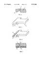
- a known power plastic packageis formed from a leadframe including a large flag portion 2, on which is mounted a semiconductor die 3.
- the semiconductor die 3is electrically connected to inner ends 4 of the lead portions 8 using gold, copper or aluminium wires 5.
- the complete assemblyis then encapsulated in an epoxy compound 1, except for the lower surface of the flag portion 2, which is left uncovered to provide a heat sink to dissipate heat from the die 3 to the external environment. Since the epoxy compound 1 does not cover the exposed heatsink, it cannot firmly lock to the leadframe.
- the lead portions 8are bent downwards to facilitate soldering of the package to a printed circuit board.
- the inner ends 4protrude towards the flag portion at a different level from the flag portion, thus allowing the epoxy compound to completely encapsulate the inner end 4 so as to improve the locking.
- the present inventiontherefore seeks to provide a leadframe structure which overcomes, or at least reduces the above-mentioned problems of the prior art.
- the inventionprovides a leadframe having at least one flag portion and at least one lead portion extending towards the flag portion, the lead portion including an elongate portion, an end portion adjacent the flag portion and an intermediate portion interconnecting the end portion and the elongate portion, the thickness of the end portion being less than the thickness of the elongate portion and the thickness of the intermediate portion being less than the thickness of the end portion.
- the end portion of the leadframehas a width greater than the elongate portion.
- the intermediate portion of the leadframehas a width greater than the elongate portion.
- the intermediate portion of the leadframehas a width substantially the same as the elongate portion.
- the elongate portion of the leadframepreferably has a thickness substantially the same as that of the flag portion and is substantially coplanar therewith.
- the inventionprovides a method of manufacturing a leadframe comprising the steps of providing a sheet of metal, stamping out of the sheet at least one flag portion connected to a first bar and at least one lead portion connected to a second bar and extending towards the flag portion, the first and second bars being interconnected by one or more tie-bars, the lead portion including an elongate portion, an end portion adjacent the flag portion and an intermediate portion interconnecting the end portion and the elongate portion, first etching the intermediate portion to a predetermined thickness, and second etching the intermediate portion and the end portion to final thicknesses, wherein the final thickness of the end portion is less than the thickness of the elongate portion and the final thickness of the intermediate portion is less than the final thickness of the end portion.
- the inventionprovides a method of packaging an electronic component, the method comprising the steps of providing a leadframe having at least one flag portion and at least one lead portion extending towards the flag portion, the lead portion including an elongate portion, an end portion adjacent the flag portion and an intermediate portion interconnecting the end portion and the elongate portion, the thickness of the end portion being less than the thickness of the elongate portion and the thickness of the intermediate portion being less than the thickness of the end portion, mounting the electronic component on the flag portion, electrically connecting the electronic component with the end portion of the lead portion, encapsulating the electronic component, the electrical connection, at least the end portion and the intermediate portion of the lead portion and at least part of the flag portion in a plastics molding compound, and curing the plastics molding compound.
- the step of providing a leadframecomprises the steps of providing a sheet of metal, stamping out of the sheet at least one flag portion connected to a first bar and at least one lead portion connected to a second bar and extending towards the flag portion, the first and second bars being interconnected by one or more tie-bars, the lead portion including an elongate portion, an end portion adjacent the flag portion and an intermediate portion interconnecting the end portion and the elongate portion, first etching the intermediate portion to a predetermined thickness, and second etching the intermediate portion and the end portion to final thicknesses, so that the final thickness of the end portion is less than the thickness of the elongate portion and the final thickness of the intermediate portion is less than the final thickness of the end portion.
- FIG. 1shows a top view of a known discrete power plastic package
- FIG. 2shows a side view of the package of FIG. 1;
- FIG. 3shows one embodiment of a discrete power package according to one embodiment of the present invention.
- FIG. 4shows an enlarged cross-sectional view of the inner end of a lead of the embodiment of FIG. 3;
- FIG. 5shows a top isometric view of the lead of FIG. 4
- FIG. 6shows a bottom isometric view of the lead of FIG. 4
- FIGS. 7 to 9show various steps in the fabrication process of the inner end of the lead of the embodiment of FIG. 3;
- FIG. 10shows the critical geometric parameters of the inner end of the lead of the embodiment of FIG. 3;
- a leadframeaccording to one embodiment of the present invention has a flag portion 2 providing a heatsink and lead portions 7, which are generally coplanar with the flag portion 2.
- a semiconductor die 3is attached to the heatsink 2 by solder material or electrical conductive epoxy (not shown) and the die 3 is electrically connected to the inner ends 6 of the lead portions 7, as before, using wire bonds 5.
- the assemblyis then encapsulated in an epoxy plastic compound, in a well known fashion.
- the inner ends 6 of the lead portions 7are chemically etched to provide a locking structure for the epoxy compound, which enable the leads to obtain sufficient z direction locking without having to downset the leadframe.
- FIG. 4shows the structure of the inner end 6 of one lead portion 7 in more detail.
- the end 6 of the lead portion 7is provided with a transverse channel 9 and the part 10 of the inner end 6 between the channel 9 and the end of the lead portion 7 is of reduced thickness to enable the mold compound to flow between the flag portion and the inner end 6 of the lead portion 7, around both sides of the reduced thickness portion 10 and into the channel 9, as best seen in FIG. 3, to provide the locking.
- the mold compoundshrinks and imposes tension stress on the channel 9.
- the leadsare held in position by the hardened mold compound.
- FIGS. 5 and 6show upper and lower perspective views of one example of a typical T-lead commonly found in multi-lead packages.
- the T-lead structure 11 at the end of the lead portion 7provides a locking effect in directions parallel and perpendicular to the elongate lead portion 7.
- the locking effect in the direction parallel to the lead portion 7is enhanced.
- the material on the lower side of the T-lead 11(as shown in FIGS. 3, 4 and 5) is etched away in a 2 step chemical etching process.
- masks made of a material unaffected by the etching substance to be usede.g. rubber
- Openingsare cut for areas to be etched.
- a mask 20is provided with a small opening 15 running along the width of the T-lead 11 in the position where the channel 9 is to be formed.
- the mask 20is then pressed onto the leadframe.
- the leadframe with the mask 20 thereonis then passed through or dipped into the chemical etching solution. The solution etches away the leadframe material and creates a small transverse groove 22 in the lead portion 7.
- another mask 21is produced, which has a larger opening 16 formed therein at the position where the reduced thickness portion 10 and the channel 9 are to be formed.
- This second mask 21is then pressed onto the leadframe. Together with the second mask 21, the leadframe is then again passed through the chemical etching solution.
- the small hole 16is enlarged by the second etching process to form the desired channel 9.
- the reduced thickness portion 10is formed, as shown in FIG. 9.
- the depth and width of the channel 9 and portion 10can be controlled by the etching time and the concentration of the chemical solution.
- FIG. 10shows the critical geometric parameters described above. They are defined as follows:
- Tis width of the T-lead structure 11 at the end of the lead portion 7;
- Lis the width of the elongate lead portion 7
- D1is the reduction in thickness of the portion 10
- D2is the depth of the channel 9
- W1is the width of the portion 10 and channel 9;
- W2is the width of the channel 9.
- the value (T-L)determines the locking effect parallel to the lead.
- the value of D1is desirably at least 0.15 mm (6 mils).
- Depth D2is preferably between 30% and 45% of the thickness of the leadframe and width W1 is preferably at least 60% of the length of the T-lead structure 11.
- width W2is between 50% and 60% of the value of width W1.
Landscapes
- Physics & Mathematics (AREA)
- Condensed Matter Physics & Semiconductors (AREA)
- General Physics & Mathematics (AREA)
- Engineering & Computer Science (AREA)
- Computer Hardware Design (AREA)
- Microelectronics & Electronic Packaging (AREA)
- Power Engineering (AREA)
- Lead Frames For Integrated Circuits (AREA)
Abstract
Description
Claims (7)
Applications Claiming Priority (2)
| Application Number | Priority Date | Filing Date | Title |
|---|---|---|---|
| MYPI9800329 | 1998-01-26 | ||
| MYPI98000329AMY118338A (en) | 1998-01-26 | 1998-01-26 | A leadframe, a method of manufacturing a leadframe and a method of packaging an electronic component utilising the leadframe. |
Publications (1)
| Publication Number | Publication Date |
|---|---|
| US5973388Atrue US5973388A (en) | 1999-10-26 |
Family
ID=19749791
Family Applications (1)
| Application Number | Title | Priority Date | Filing Date |
|---|---|---|---|
| US09/224,823Expired - LifetimeUS5973388A (en) | 1998-01-26 | 1999-01-04 | Leadframe, method of manufacturing a leadframe, and method of packaging an electronic component utilizing the leadframe |
Country Status (3)
| Country | Link |
|---|---|
| US (1) | US5973388A (en) |
| JP (1) | JPH11260980A (en) |
| MY (1) | MY118338A (en) |
Cited By (118)
| Publication number | Priority date | Publication date | Assignee | Title |
|---|---|---|---|---|
| US6166430A (en)* | 1998-05-27 | 2000-12-26 | Matsushita Electronics Corporation | Lead frame, method for manufacturing the frame, resin-molded semiconductor device and method for manufacturing the device |
| US6198171B1 (en)* | 1999-12-30 | 2001-03-06 | Siliconware Precision Industries Co., Ltd. | Thermally enhanced quad flat non-lead package of semiconductor |
| US6252306B1 (en)* | 1998-05-12 | 2001-06-26 | Mitsubishi Denki Kabushiki Kaisha | Method of producing semiconductor device and configuration thereof, and lead frame used in said method |
| US6469398B1 (en)* | 2001-03-29 | 2002-10-22 | Kabushiki Kaisha Toshiba | Semiconductor package and manufacturing method thereof |
| US6483178B1 (en)* | 2000-07-14 | 2002-11-19 | Siliconware Precision Industries Co., Ltd. | Semiconductor device package structure |
| US20030020146A1 (en)* | 1998-11-20 | 2003-01-30 | Yee Jae Hak | Semiconductor package and method of making using leadframe having lead locks to secure leads to encapsulant |
| DE10155139A1 (en)* | 2001-11-12 | 2003-02-27 | Infineon Technologies Ag | Electronic component comprises a semiconductor element mounted in a plastic housing, and electrical connections arranged between contact surfaces on an active surface of the element and contact connecting surfaces of conductor connections |
| US6563199B2 (en)* | 2000-03-21 | 2003-05-13 | Mitsui High-Tec Inc. | Lead frame for semiconductor devices, a semiconductor device made using the lead frame |
| US20030089975A1 (en)* | 2000-03-07 | 2003-05-15 | Yasuji Hiramatsu | Ceramic substrate for manufacture/inspection of semiconductor |
| US6589814B1 (en) | 1998-04-02 | 2003-07-08 | National Semiconductor Corporation | Lead frame chip scale package |
| US20030168719A1 (en)* | 2002-03-06 | 2003-09-11 | Cheng Man Hon | Multi-row leadframe |
| US6630728B2 (en) | 1998-06-24 | 2003-10-07 | Amkor Technology, Inc. | Plastic integrated circuit package and leadframe for making the package |
| US20030234454A1 (en)* | 2002-06-24 | 2003-12-25 | Serafin Pedron | Integrated circuit package and method of manufacturing the integrated circuit package |
| US6703695B2 (en)* | 2002-03-22 | 2004-03-09 | Sharp Kabushiki Kaisha | Semiconductor device and method for producing the same |
| US20040063244A1 (en)* | 2002-09-23 | 2004-04-01 | Mahle Richard L. | Leadframe-to-plastic lock for IC package |
| US6750545B1 (en) | 2003-02-28 | 2004-06-15 | Amkor Technology, Inc. | Semiconductor package capable of die stacking |
| US6756658B1 (en)* | 2001-04-06 | 2004-06-29 | Amkor Technology, Inc. | Making two lead surface mounting high power microleadframe semiconductor packages |
| US20040150086A1 (en)* | 1999-10-15 | 2004-08-05 | Lee Tae Heon | Semiconductor package having reduced thickness |
| US20040150077A1 (en)* | 2000-11-01 | 2004-08-05 | Katsufusa Fujita | Lead frame and semiconductor device using this |
| US6777789B1 (en) | 2001-03-20 | 2004-08-17 | Amkor Technology, Inc. | Mounting for a package containing a chip |
| US6794740B1 (en) | 2003-03-13 | 2004-09-21 | Amkor Technology, Inc. | Leadframe package for semiconductor devices |
| US6798047B1 (en) | 2002-12-26 | 2004-09-28 | Amkor Technology, Inc. | Pre-molded leadframe |
| US6818973B1 (en) | 2002-09-09 | 2004-11-16 | Amkor Technology, Inc. | Exposed lead QFP package fabricated through the use of a partial saw process |
| US6841414B1 (en) | 2002-06-19 | 2005-01-11 | Amkor Technology, Inc. | Saw and etch singulation method for a chip package |
| US6846704B2 (en) | 2001-03-27 | 2005-01-25 | Amkor Technology, Inc. | Semiconductor package and method for manufacturing the same |
| US6867071B1 (en) | 2002-07-12 | 2005-03-15 | Amkor Technology, Inc. | Leadframe including corner leads and semiconductor package using same |
| US6873041B1 (en) | 2001-11-07 | 2005-03-29 | Amkor Technology, Inc. | Power semiconductor package with strap |
| US6879034B1 (en) | 2003-05-01 | 2005-04-12 | Amkor Technology, Inc. | Semiconductor package including low temperature co-fired ceramic substrate |
| US6891276B1 (en)* | 2002-01-09 | 2005-05-10 | Bridge Semiconductor Corporation | Semiconductor package device |
| US6893900B1 (en) | 1998-06-24 | 2005-05-17 | Amkor Technology, Inc. | Method of making an integrated circuit package |
| US6897550B1 (en) | 2003-06-11 | 2005-05-24 | Amkor Technology, Inc. | Fully-molded leadframe stand-off feature |
| US6919620B1 (en) | 2002-09-17 | 2005-07-19 | Amkor Technology, Inc. | Compact flash memory card with clamshell leadframe |
| US20050156292A1 (en)* | 2001-01-15 | 2005-07-21 | Paek Jong S. | Reduced size semiconductor package with stacked dies |
| US6921967B2 (en) | 2003-09-24 | 2005-07-26 | Amkor Technology, Inc. | Reinforced die pad support structure |
| US6927483B1 (en) | 2003-03-07 | 2005-08-09 | Amkor Technology, Inc. | Semiconductor package exhibiting efficient lead placement |
| US6936495B1 (en) | 2002-01-09 | 2005-08-30 | Bridge Semiconductor Corporation | Method of making an optoelectronic semiconductor package device |
| US6953988B2 (en) | 2000-03-25 | 2005-10-11 | Amkor Technology, Inc. | Semiconductor package |
| US6965157B1 (en)* | 1999-11-09 | 2005-11-15 | Amkor Technology, Inc. | Semiconductor package with exposed die pad and body-locking leadframe |
| US6965159B1 (en) | 2001-09-19 | 2005-11-15 | Amkor Technology, Inc. | Reinforced lead-frame assembly for interconnecting circuits within a circuit module |
| US6967395B1 (en) | 2001-03-20 | 2005-11-22 | Amkor Technology, Inc. | Mounting for a package containing a chip |
| US6987034B1 (en) | 2002-01-09 | 2006-01-17 | Bridge Semiconductor Corporation | Method of making a semiconductor package device that includes singulating and trimming a lead |
| US7001799B1 (en) | 2003-03-13 | 2006-02-21 | Amkor Technology, Inc. | Method of making a leadframe for semiconductor devices |
| US7005326B1 (en) | 1998-06-24 | 2006-02-28 | Amkor Technology, Inc. | Method of making an integrated circuit package |
| US7008825B1 (en) | 2003-05-27 | 2006-03-07 | Amkor Technology, Inc. | Leadframe strip having enhanced testability |
| US7030474B1 (en) | 1998-06-24 | 2006-04-18 | Amkor Technology, Inc. | Plastic integrated circuit package and method and leadframe for making the package |
| US7045396B2 (en) | 1999-12-16 | 2006-05-16 | Amkor Technology, Inc. | Stackable semiconductor package and method for manufacturing same |
| US7045882B2 (en) | 2000-12-29 | 2006-05-16 | Amkor Technology, Inc. | Semiconductor package including flip chip |
| US7045883B1 (en) | 2001-04-04 | 2006-05-16 | Amkor Technology, Inc. | Thermally enhanced chip scale lead on chip semiconductor package and method of making same |
| US7057268B1 (en) | 2004-01-27 | 2006-06-06 | Amkor Technology, Inc. | Cavity case with clip/plug for use on multi-media card |
| US7064009B1 (en) | 2001-04-04 | 2006-06-20 | Amkor Technology, Inc. | Thermally enhanced chip scale lead on chip semiconductor package and method of making same |
| US7067908B2 (en) | 1999-10-15 | 2006-06-27 | Amkor Technology, Inc. | Semiconductor package having improved adhesiveness and ground bonding |
| US7071541B1 (en) | 1998-06-24 | 2006-07-04 | Amkor Technology, Inc. | Plastic integrated circuit package and method and leadframe for making the package |
| US20060151858A1 (en)* | 2000-04-27 | 2006-07-13 | Ahn Byung H | Leadframe and semiconductor package made using the leadframe |
| US7091594B1 (en) | 2004-01-28 | 2006-08-15 | Amkor Technology, Inc. | Leadframe type semiconductor package having reduced inductance and its manufacturing method |
| US20060181861A1 (en)* | 2005-02-17 | 2006-08-17 | Walker Harold Y Jr | Etched leadframe for reducing metal gaps |
| US7095103B1 (en) | 2003-05-01 | 2006-08-22 | Amkor Technology, Inc. | Leadframe based memory card |
| US7102208B1 (en) | 1999-10-15 | 2006-09-05 | Amkor Technology, Inc. | Leadframe and semiconductor package with improved solder joint strength |
| US7112474B1 (en) | 1998-06-24 | 2006-09-26 | Amkor Technology, Inc. | Method of making an integrated circuit package |
| US7138707B1 (en) | 2003-10-21 | 2006-11-21 | Amkor Technology, Inc. | Semiconductor package including leads and conductive posts for providing increased functionality |
| US7170150B2 (en) | 2001-03-27 | 2007-01-30 | Amkor Technology, Inc. | Lead frame for semiconductor package |
| US7183630B1 (en) | 2002-04-15 | 2007-02-27 | Amkor Technology, Inc. | Lead frame with plated end leads |
| US7190062B1 (en) | 2004-06-15 | 2007-03-13 | Amkor Technology, Inc. | Embedded leadframe semiconductor package |
| US7190060B1 (en) | 2002-01-09 | 2007-03-13 | Bridge Semiconductor Corporation | Three-dimensional stacked semiconductor package device with bent and flat leads and method of making same |
| US7192807B1 (en) | 2002-11-08 | 2007-03-20 | Amkor Technology, Inc. | Wafer level package and fabrication method |
| US7202554B1 (en) | 2004-08-19 | 2007-04-10 | Amkor Technology, Inc. | Semiconductor package and its manufacturing method |
| US7211879B1 (en) | 2003-11-12 | 2007-05-01 | Amkor Technology, Inc. | Semiconductor package with chamfered corners and method of manufacturing the same |
| US7214326B1 (en) | 2003-11-07 | 2007-05-08 | Amkor Technology, Inc. | Increased capacity leadframe and semiconductor package using the same |
| US7217991B1 (en) | 2004-10-22 | 2007-05-15 | Amkor Technology, Inc. | Fan-in leadframe semiconductor package |
| US20070126092A1 (en)* | 2005-12-02 | 2007-06-07 | Advanced Interconnect Technologies Limited, A Corporation Of The Republic Of Mauritius | Leadless semiconductor package and method of manufacture |
| US7245007B1 (en) | 2003-09-18 | 2007-07-17 | Amkor Technology, Inc. | Exposed lead interposer leadframe package |
| US7253503B1 (en) | 1999-11-05 | 2007-08-07 | Amkor Technology, Inc. | Integrated circuit device packages and substrates for making the packages |
| US20070241423A1 (en)* | 2006-04-14 | 2007-10-18 | Taylor William P | Methods and apparatus for integrated circuit having multiple dies with at least one on chip capacitor |
| US20070278629A1 (en)* | 2006-06-06 | 2007-12-06 | International Business Machines Corporation | Method and structure for improving the reliability of leadframe integrated circuit packages |
| US20080034582A1 (en)* | 2006-04-14 | 2008-02-14 | Taylor William P | Methods for sensor having capacitor on chip |
| US7332375B1 (en) | 1998-06-24 | 2008-02-19 | Amkor Technology, Inc. | Method of making an integrated circuit package |
| US20080067698A1 (en)* | 2006-09-15 | 2008-03-20 | Stats Chippac Ltd. | Integrated circuit package system with encapsulation lock |
| US20080067639A1 (en)* | 2006-09-15 | 2008-03-20 | Stats Chippac Ltd. | Integrated circuit package system with encapsulation lock |
| US20080067640A1 (en)* | 2006-09-15 | 2008-03-20 | Stats Chippac Ltd. | Integrated circuit package system with encapsulation lock |
| US7361533B1 (en) | 2002-11-08 | 2008-04-22 | Amkor Technology, Inc. | Stacked embedded leadframe |
| US20080122049A1 (en)* | 2006-11-28 | 2008-05-29 | Texas Instruments Incorporated | Leadframe finger design to ensure lead-locking for enhanced fatigue life of bonding wire in an overmolded package |
| JP2008538971A (en)* | 2005-04-29 | 2008-11-13 | コーニンクレッカ フィリップス エレクトロニクス エヌ ヴィ | Energy-resolved photon counting for CT |
| US20080290484A1 (en)* | 2005-07-20 | 2008-11-27 | Infineon Technologies Ag | Leadframe Strip and Mold Apparatus for an Electronic Component and Method of Encapsulating an Electronic Component |
| US7485952B1 (en) | 2001-09-19 | 2009-02-03 | Amkor Technology, Inc. | Drop resistant bumpers for fully molded memory cards |
| US20090072364A1 (en)* | 2007-09-13 | 2009-03-19 | Punzalan Jeffrey D | Integrated circuit package system with leads separated from a die paddle |
| US7507603B1 (en) | 2005-12-02 | 2009-03-24 | Amkor Technology, Inc. | Etch singulated semiconductor package |
| US7572681B1 (en) | 2005-12-08 | 2009-08-11 | Amkor Technology, Inc. | Embedded electronic component package |
| US20100052424A1 (en)* | 2008-08-26 | 2010-03-04 | Taylor William P | Methods and apparatus for integrated circuit having integrated energy storage device |
| US7723210B2 (en) | 2002-11-08 | 2010-05-25 | Amkor Technology, Inc. | Direct-write wafer level chip scale package |
| US7902660B1 (en) | 2006-05-24 | 2011-03-08 | Amkor Technology, Inc. | Substrate for semiconductor device and manufacturing method thereof |
| US7968998B1 (en) | 2006-06-21 | 2011-06-28 | Amkor Technology, Inc. | Side leaded, bottom exposed pad and bottom exposed lead fusion quad flat semiconductor package |
| US8093670B2 (en) | 2008-07-24 | 2012-01-10 | Allegro Microsystems, Inc. | Methods and apparatus for integrated circuit having on chip capacitor with eddy current reductions |
| US8294276B1 (en) | 2010-05-27 | 2012-10-23 | Amkor Technology, Inc. | Semiconductor device and fabricating method thereof |
| US8324511B1 (en) | 2010-04-06 | 2012-12-04 | Amkor Technology, Inc. | Through via nub reveal method and structure |
| US8390130B1 (en) | 2011-01-06 | 2013-03-05 | Amkor Technology, Inc. | Through via recessed reveal structure and method |
| US8440554B1 (en) | 2010-08-02 | 2013-05-14 | Amkor Technology, Inc. | Through via connected backside embedded circuit features structure and method |
| US8487445B1 (en) | 2010-10-05 | 2013-07-16 | Amkor Technology, Inc. | Semiconductor device having through electrodes protruding from dielectric layer |
| US8552548B1 (en) | 2011-11-29 | 2013-10-08 | Amkor Technology, Inc. | Conductive pad on protruding through electrode semiconductor device |
| US8629539B2 (en) | 2012-01-16 | 2014-01-14 | Allegro Microsystems, Llc | Methods and apparatus for magnetic sensor having non-conductive die paddle |
| US8791501B1 (en) | 2010-12-03 | 2014-07-29 | Amkor Technology, Inc. | Integrated passive device structure and method |
| US8796561B1 (en) | 2009-10-05 | 2014-08-05 | Amkor Technology, Inc. | Fan out build up substrate stackable package and method |
| US20150014835A1 (en)* | 2012-06-29 | 2015-01-15 | Intersil Americas LLC | Solder flow impeding feature on a lead frame |
| US20150014845A1 (en)* | 2013-07-11 | 2015-01-15 | Infineon Technologies Ag | Semiconductor module with interlocked connection |
| US8937381B1 (en) | 2009-12-03 | 2015-01-20 | Amkor Technology, Inc. | Thin stackable package and method |
| US9048298B1 (en) | 2012-03-29 | 2015-06-02 | Amkor Technology, Inc. | Backside warpage control structure and fabrication method |
| US9129943B1 (en) | 2012-03-29 | 2015-09-08 | Amkor Technology, Inc. | Embedded component package and fabrication method |
| US9228860B2 (en) | 2006-07-14 | 2016-01-05 | Allegro Microsystems, Llc | Sensor and method of providing a sensor |
| US9411025B2 (en) | 2013-04-26 | 2016-08-09 | Allegro Microsystems, Llc | Integrated circuit package having a split lead frame and a magnet |
| US9494660B2 (en) | 2012-03-20 | 2016-11-15 | Allegro Microsystems, Llc | Integrated circuit package having a split lead frame |
| US9666788B2 (en) | 2012-03-20 | 2017-05-30 | Allegro Microsystems, Llc | Integrated circuit package having a split lead frame |
| US9691734B1 (en) | 2009-12-07 | 2017-06-27 | Amkor Technology, Inc. | Method of forming a plurality of electronic component packages |
| US9812588B2 (en) | 2012-03-20 | 2017-11-07 | Allegro Microsystems, Llc | Magnetic field sensor integrated circuit with integral ferromagnetic material |
| US20180158770A1 (en)* | 2014-03-07 | 2018-06-07 | Bridge Semiconductor Corp. | Methods of making wiring substrate for stackable semiconductor assembly and making stackable semiconductor assembly |
| US10234513B2 (en) | 2012-03-20 | 2019-03-19 | Allegro Microsystems, Llc | Magnetic field sensor integrated circuit with integral ferromagnetic material |
| US10411498B2 (en) | 2015-10-21 | 2019-09-10 | Allegro Microsystems, Llc | Apparatus and methods for extending sensor integrated circuit operation through a power disturbance |
| US20200227343A1 (en)* | 2019-01-11 | 2020-07-16 | Chang Wah Technology Co., Ltd. | Semiconductor device package |
| US10978897B2 (en) | 2018-04-02 | 2021-04-13 | Allegro Microsystems, Llc | Systems and methods for suppressing undesirable voltage supply artifacts |
| US10991644B2 (en) | 2019-08-22 | 2021-04-27 | Allegro Microsystems, Llc | Integrated circuit package having a low profile |
| US11291146B2 (en)* | 2014-03-07 | 2022-03-29 | Bridge Semiconductor Corp. | Leadframe substrate having modulator and crack inhibiting structure and flip chip assembly using the same |
Families Citing this family (2)
| Publication number | Priority date | Publication date | Assignee | Title |
|---|---|---|---|---|
| KR100426494B1 (en)* | 1999-12-20 | 2004-04-13 | 앰코 테크놀로지 코리아 주식회사 | Semiconductor package and its manufacturing method |
| JP6549003B2 (en)* | 2015-09-18 | 2019-07-24 | エイブリック株式会社 | Semiconductor device |
Citations (11)
| Publication number | Priority date | Publication date | Assignee | Title |
|---|---|---|---|---|
| JPS54140465A (en)* | 1978-04-24 | 1979-10-31 | Hitachi Ltd | Lead frame |
| JPS5662344A (en)* | 1979-10-26 | 1981-05-28 | Hitachi Ltd | Resin sealed semiconductor device |
| JPS59222951A (en)* | 1983-06-02 | 1984-12-14 | Sumitomo Electric Ind Ltd | Lead frame for semiconductor devices |
| JPS61224441A (en)* | 1985-03-29 | 1986-10-06 | Nec Corp | Lead frame |
| JPH01186662A (en)* | 1988-01-14 | 1989-07-26 | Mitsui High Tec Inc | Lead frame for semiconductor device |
| JPH01289149A (en)* | 1988-05-17 | 1989-11-21 | Sumitomo Metal Mining Co Ltd | Two-stage coining lead frame |
| JPH01289150A (en)* | 1988-05-17 | 1989-11-21 | Sumitomo Metal Mining Co Ltd | Solder-clad lead frame and manufacture thereof |
| JPH04364061A (en)* | 1991-06-11 | 1992-12-16 | Mitsui High Tec Inc | Manufacture of lead frame |
| JPH04368154A (en)* | 1991-06-15 | 1992-12-21 | Sony Corp | Semiconductor device |
| JPH05109928A (en)* | 1991-10-14 | 1993-04-30 | Mitsubishi Electric Corp | Lead frame for resin-sealed semiconductor device and resin-sealed semiconductor device using the same |
| JPH0621305A (en)* | 1992-06-30 | 1994-01-28 | Matsushita Electron Corp | Semiconductor device |
- 1998
- 1998-01-26MYMYPI98000329Apatent/MY118338A/enunknown
- 1999
- 1999-01-04USUS09/224,823patent/US5973388A/ennot_activeExpired - Lifetime
- 1999-01-25JPJP11015153Apatent/JPH11260980A/enactivePending
Patent Citations (11)
| Publication number | Priority date | Publication date | Assignee | Title |
|---|---|---|---|---|
| JPS54140465A (en)* | 1978-04-24 | 1979-10-31 | Hitachi Ltd | Lead frame |
| JPS5662344A (en)* | 1979-10-26 | 1981-05-28 | Hitachi Ltd | Resin sealed semiconductor device |
| JPS59222951A (en)* | 1983-06-02 | 1984-12-14 | Sumitomo Electric Ind Ltd | Lead frame for semiconductor devices |
| JPS61224441A (en)* | 1985-03-29 | 1986-10-06 | Nec Corp | Lead frame |
| JPH01186662A (en)* | 1988-01-14 | 1989-07-26 | Mitsui High Tec Inc | Lead frame for semiconductor device |
| JPH01289149A (en)* | 1988-05-17 | 1989-11-21 | Sumitomo Metal Mining Co Ltd | Two-stage coining lead frame |
| JPH01289150A (en)* | 1988-05-17 | 1989-11-21 | Sumitomo Metal Mining Co Ltd | Solder-clad lead frame and manufacture thereof |
| JPH04364061A (en)* | 1991-06-11 | 1992-12-16 | Mitsui High Tec Inc | Manufacture of lead frame |
| JPH04368154A (en)* | 1991-06-15 | 1992-12-21 | Sony Corp | Semiconductor device |
| JPH05109928A (en)* | 1991-10-14 | 1993-04-30 | Mitsubishi Electric Corp | Lead frame for resin-sealed semiconductor device and resin-sealed semiconductor device using the same |
| JPH0621305A (en)* | 1992-06-30 | 1994-01-28 | Matsushita Electron Corp | Semiconductor device |
Cited By (205)
| Publication number | Priority date | Publication date | Assignee | Title |
|---|---|---|---|---|
| US6589814B1 (en) | 1998-04-02 | 2003-07-08 | National Semiconductor Corporation | Lead frame chip scale package |
| USRE39854E1 (en) | 1998-04-02 | 2007-09-25 | National Semiconductor Corporation | Lead frame chip scale package |
| US6888228B1 (en)* | 1998-04-02 | 2005-05-03 | National Semiconductor Corporation | Lead frame chip scale package |
| US6252306B1 (en)* | 1998-05-12 | 2001-06-26 | Mitsubishi Denki Kabushiki Kaisha | Method of producing semiconductor device and configuration thereof, and lead frame used in said method |
| US6372546B2 (en)* | 1998-05-12 | 2002-04-16 | Mitsubishi Denki Kabushiki Kaisha | Method of producing semiconductor device and configuration thereof, and lead frame used in said method |
| US6166430A (en)* | 1998-05-27 | 2000-12-26 | Matsushita Electronics Corporation | Lead frame, method for manufacturing the frame, resin-molded semiconductor device and method for manufacturing the device |
| US6630728B2 (en) | 1998-06-24 | 2003-10-07 | Amkor Technology, Inc. | Plastic integrated circuit package and leadframe for making the package |
| US7332375B1 (en) | 1998-06-24 | 2008-02-19 | Amkor Technology, Inc. | Method of making an integrated circuit package |
| US7005326B1 (en) | 1998-06-24 | 2006-02-28 | Amkor Technology, Inc. | Method of making an integrated circuit package |
| US7030474B1 (en) | 1998-06-24 | 2006-04-18 | Amkor Technology, Inc. | Plastic integrated circuit package and method and leadframe for making the package |
| US8853836B1 (en) | 1998-06-24 | 2014-10-07 | Amkor Technology, Inc. | Integrated circuit package and method of making the same |
| US9224676B1 (en) | 1998-06-24 | 2015-12-29 | Amkor Technology, Inc. | Integrated circuit package and method of making the same |
| US8963301B1 (en) | 1998-06-24 | 2015-02-24 | Amkor Technology, Inc. | Integrated circuit package and method of making the same |
| US7071541B1 (en) | 1998-06-24 | 2006-07-04 | Amkor Technology, Inc. | Plastic integrated circuit package and method and leadframe for making the package |
| US6893900B1 (en) | 1998-06-24 | 2005-05-17 | Amkor Technology, Inc. | Method of making an integrated circuit package |
| US7112474B1 (en) | 1998-06-24 | 2006-09-26 | Amkor Technology, Inc. | Method of making an integrated circuit package |
| US8318287B1 (en) | 1998-06-24 | 2012-11-27 | Amkor Technology, Inc. | Integrated circuit package and method of making the same |
| US7564122B2 (en) | 1998-11-20 | 2009-07-21 | Amkor Technology, Inc. | Semiconductor package and method of making using leadframe having lead locks to secure leads to encapsulant |
| US6825062B2 (en) | 1998-11-20 | 2004-11-30 | Amkor Technology, Inc. | Semiconductor package and method of making using leadframe having lead locks to secure leads to encapsulant |
| US20030020146A1 (en)* | 1998-11-20 | 2003-01-30 | Yee Jae Hak | Semiconductor package and method of making using leadframe having lead locks to secure leads to encapsulant |
| US7057280B2 (en) | 1998-11-20 | 2006-06-06 | Amkor Technology, Inc. | Leadframe having lead locks to secure leads to encapsulant |
| US7067908B2 (en) | 1999-10-15 | 2006-06-27 | Amkor Technology, Inc. | Semiconductor package having improved adhesiveness and ground bonding |
| US7321162B1 (en) | 1999-10-15 | 2008-01-22 | Amkor Technology, Inc. | Semiconductor package having reduced thickness |
| US7102208B1 (en) | 1999-10-15 | 2006-09-05 | Amkor Technology, Inc. | Leadframe and semiconductor package with improved solder joint strength |
| US7535085B2 (en) | 1999-10-15 | 2009-05-19 | Amkor Technology, Inc. | Semiconductor package having improved adhesiveness and ground bonding |
| US7115445B2 (en) | 1999-10-15 | 2006-10-03 | Amkor Technology, Inc. | Semiconductor package having reduced thickness |
| US20040150086A1 (en)* | 1999-10-15 | 2004-08-05 | Lee Tae Heon | Semiconductor package having reduced thickness |
| US7253503B1 (en) | 1999-11-05 | 2007-08-07 | Amkor Technology, Inc. | Integrated circuit device packages and substrates for making the packages |
| US6965157B1 (en)* | 1999-11-09 | 2005-11-15 | Amkor Technology, Inc. | Semiconductor package with exposed die pad and body-locking leadframe |
| US7045396B2 (en) | 1999-12-16 | 2006-05-16 | Amkor Technology, Inc. | Stackable semiconductor package and method for manufacturing same |
| US6198171B1 (en)* | 1999-12-30 | 2001-03-06 | Siliconware Precision Industries Co., Ltd. | Thermally enhanced quad flat non-lead package of semiconductor |
| US20040207072A1 (en)* | 2000-03-07 | 2004-10-21 | Ibiden Co., Ltd. | Ceramic substrate for a semiconductor producing/examining device |
| US20030089975A1 (en)* | 2000-03-07 | 2003-05-15 | Yasuji Hiramatsu | Ceramic substrate for manufacture/inspection of semiconductor |
| US6888236B2 (en)* | 2000-03-07 | 2005-05-03 | Ibiden Co., Ltd. | Ceramic substrate for manufacture/inspection of semiconductor |
| US6563199B2 (en)* | 2000-03-21 | 2003-05-13 | Mitsui High-Tec Inc. | Lead frame for semiconductor devices, a semiconductor device made using the lead frame |
| US6953988B2 (en) | 2000-03-25 | 2005-10-11 | Amkor Technology, Inc. | Semiconductor package |
| US20060151858A1 (en)* | 2000-04-27 | 2006-07-13 | Ahn Byung H | Leadframe and semiconductor package made using the leadframe |
| US9362210B2 (en)* | 2000-04-27 | 2016-06-07 | Amkor Technology, Inc. | Leadframe and semiconductor package made using the leadframe |
| US8410585B2 (en)* | 2000-04-27 | 2013-04-02 | Amkor Technology, Inc. | Leadframe and semiconductor package made using the leadframe |
| US6483178B1 (en)* | 2000-07-14 | 2002-11-19 | Siliconware Precision Industries Co., Ltd. | Semiconductor device package structure |
| US20040150077A1 (en)* | 2000-11-01 | 2004-08-05 | Katsufusa Fujita | Lead frame and semiconductor device using this |
| US6936915B2 (en)* | 2000-11-01 | 2005-08-30 | Mitsui High-Tec, Inc. | Lead frame having chip mounting part and leads of different thicknesses |
| US7045882B2 (en) | 2000-12-29 | 2006-05-16 | Amkor Technology, Inc. | Semiconductor package including flip chip |
| US20050156292A1 (en)* | 2001-01-15 | 2005-07-21 | Paek Jong S. | Reduced size semiconductor package with stacked dies |
| US6777789B1 (en) | 2001-03-20 | 2004-08-17 | Amkor Technology, Inc. | Mounting for a package containing a chip |
| US6967395B1 (en) | 2001-03-20 | 2005-11-22 | Amkor Technology, Inc. | Mounting for a package containing a chip |
| US7170150B2 (en) | 2001-03-27 | 2007-01-30 | Amkor Technology, Inc. | Lead frame for semiconductor package |
| US7521294B2 (en) | 2001-03-27 | 2009-04-21 | Amkor Technology, Inc. | Lead frame for semiconductor package |
| US6846704B2 (en) | 2001-03-27 | 2005-01-25 | Amkor Technology, Inc. | Semiconductor package and method for manufacturing the same |
| US6469398B1 (en)* | 2001-03-29 | 2002-10-22 | Kabushiki Kaisha Toshiba | Semiconductor package and manufacturing method thereof |
| US7045883B1 (en) | 2001-04-04 | 2006-05-16 | Amkor Technology, Inc. | Thermally enhanced chip scale lead on chip semiconductor package and method of making same |
| US7064009B1 (en) | 2001-04-04 | 2006-06-20 | Amkor Technology, Inc. | Thermally enhanced chip scale lead on chip semiconductor package and method of making same |
| US6756658B1 (en)* | 2001-04-06 | 2004-06-29 | Amkor Technology, Inc. | Making two lead surface mounting high power microleadframe semiconductor packages |
| US6965159B1 (en) | 2001-09-19 | 2005-11-15 | Amkor Technology, Inc. | Reinforced lead-frame assembly for interconnecting circuits within a circuit module |
| US7176062B1 (en) | 2001-09-19 | 2007-02-13 | Amkor Technology, Inc. | Lead-frame method and assembly for interconnecting circuits within a circuit module |
| US6998702B1 (en) | 2001-09-19 | 2006-02-14 | Amkor Technology, Inc. | Front edge chamfer feature for fully-molded memory cards |
| US7485952B1 (en) | 2001-09-19 | 2009-02-03 | Amkor Technology, Inc. | Drop resistant bumpers for fully molded memory cards |
| US6873041B1 (en) | 2001-11-07 | 2005-03-29 | Amkor Technology, Inc. | Power semiconductor package with strap |
| DE10155139A1 (en)* | 2001-11-12 | 2003-02-27 | Infineon Technologies Ag | Electronic component comprises a semiconductor element mounted in a plastic housing, and electrical connections arranged between contact surfaces on an active surface of the element and contact connecting surfaces of conductor connections |
| US6936495B1 (en) | 2002-01-09 | 2005-08-30 | Bridge Semiconductor Corporation | Method of making an optoelectronic semiconductor package device |
| US7009309B1 (en) | 2002-01-09 | 2006-03-07 | Bridge Semiconductor Corporation | Semiconductor package device that includes an insulative housing with a protruding peripheral portion |
| US6987034B1 (en) | 2002-01-09 | 2006-01-17 | Bridge Semiconductor Corporation | Method of making a semiconductor package device that includes singulating and trimming a lead |
| US6908794B1 (en) | 2002-01-09 | 2005-06-21 | Bridge Semiconductor Corporation | Method of making a semiconductor package device that includes a conductive trace with recessed and non-recessed portions |
| US6989584B1 (en) | 2002-01-09 | 2006-01-24 | Bridge Semiconductor Corporation | Semiconductor package device that includes a conductive trace with a routing line, a terminal and a lead |
| US6989295B1 (en) | 2002-01-09 | 2006-01-24 | Bridge Semiconductor Corporation | Method of making a semiconductor package device that includes an insulative housing with first and second housing portions |
| US6891276B1 (en)* | 2002-01-09 | 2005-05-10 | Bridge Semiconductor Corporation | Semiconductor package device |
| US7190060B1 (en) | 2002-01-09 | 2007-03-13 | Bridge Semiconductor Corporation | Three-dimensional stacked semiconductor package device with bent and flat leads and method of making same |
| US20030168719A1 (en)* | 2002-03-06 | 2003-09-11 | Cheng Man Hon | Multi-row leadframe |
| US6838751B2 (en) | 2002-03-06 | 2005-01-04 | Freescale Semiconductor Inc. | Multi-row leadframe |
| US6703695B2 (en)* | 2002-03-22 | 2004-03-09 | Sharp Kabushiki Kaisha | Semiconductor device and method for producing the same |
| US7183630B1 (en) | 2002-04-15 | 2007-02-27 | Amkor Technology, Inc. | Lead frame with plated end leads |
| US6841414B1 (en) | 2002-06-19 | 2005-01-11 | Amkor Technology, Inc. | Saw and etch singulation method for a chip package |
| US6940154B2 (en)* | 2002-06-24 | 2005-09-06 | Asat Limited | Integrated circuit package and method of manufacturing the integrated circuit package |
| US20030234454A1 (en)* | 2002-06-24 | 2003-12-25 | Serafin Pedron | Integrated circuit package and method of manufacturing the integrated circuit package |
| US6867071B1 (en) | 2002-07-12 | 2005-03-15 | Amkor Technology, Inc. | Leadframe including corner leads and semiconductor package using same |
| US7211471B1 (en) | 2002-09-09 | 2007-05-01 | Amkor Technology, Inc. | Exposed lead QFP package fabricated through the use of a partial saw process |
| US6876068B1 (en) | 2002-09-09 | 2005-04-05 | Amkor Technology, Inc | Semiconductor package with increased number of input and output pins |
| US6995459B2 (en) | 2002-09-09 | 2006-02-07 | Amkor Technology, Inc. | Semiconductor package with increased number of input and output pins |
| US6818973B1 (en) | 2002-09-09 | 2004-11-16 | Amkor Technology, Inc. | Exposed lead QFP package fabricated through the use of a partial saw process |
| US6919620B1 (en) | 2002-09-17 | 2005-07-19 | Amkor Technology, Inc. | Compact flash memory card with clamshell leadframe |
| US20040063244A1 (en)* | 2002-09-23 | 2004-04-01 | Mahle Richard L. | Leadframe-to-plastic lock for IC package |
| US6794738B2 (en)* | 2002-09-23 | 2004-09-21 | Texas Instruments Incorporated | Leadframe-to-plastic lock for IC package |
| US8691632B1 (en) | 2002-11-08 | 2014-04-08 | Amkor Technology, Inc. | Wafer level package and fabrication method |
| US7420272B1 (en) | 2002-11-08 | 2008-09-02 | Amkor Technology, Inc. | Two-sided wafer escape package |
| US7192807B1 (en) | 2002-11-08 | 2007-03-20 | Amkor Technology, Inc. | Wafer level package and fabrication method |
| US8486764B1 (en) | 2002-11-08 | 2013-07-16 | Amkor Technology, Inc. | Wafer level package and fabrication method |
| US7714431B1 (en) | 2002-11-08 | 2010-05-11 | Amkor Technology, Inc. | Electronic component package comprising fan-out and fan-in traces |
| US7692286B1 (en) | 2002-11-08 | 2010-04-06 | Amkor Technology, Inc. | Two-sided fan-out wafer escape package |
| US9054117B1 (en) | 2002-11-08 | 2015-06-09 | Amkor Technology, Inc. | Wafer level package and fabrication method |
| US8501543B1 (en) | 2002-11-08 | 2013-08-06 | Amkor Technology, Inc. | Direct-write wafer level chip scale package |
| US8119455B1 (en) | 2002-11-08 | 2012-02-21 | Amkor Technology, Inc. | Wafer level package fabrication method |
| US7247523B1 (en) | 2002-11-08 | 2007-07-24 | Amkor Technology, Inc. | Two-sided wafer escape package |
| US7932595B1 (en) | 2002-11-08 | 2011-04-26 | Amkor Technology, Inc. | Electronic component package comprising fan-out traces |
| US8188584B1 (en) | 2002-11-08 | 2012-05-29 | Amkor Technology, Inc. | Direct-write wafer level chip scale package |
| US8710649B1 (en) | 2002-11-08 | 2014-04-29 | Amkor Technology, Inc. | Wafer level package and fabrication method |
| US8298866B1 (en) | 2002-11-08 | 2012-10-30 | Amkor Technology, Inc. | Wafer level package and fabrication method |
| US7723210B2 (en) | 2002-11-08 | 2010-05-25 | Amkor Technology, Inc. | Direct-write wafer level chip scale package |
| US8952522B1 (en) | 2002-11-08 | 2015-02-10 | Amkor Technology, Inc. | Wafer level package and fabrication method |
| US9406645B1 (en) | 2002-11-08 | 2016-08-02 | Amkor Technology, Inc. | Wafer level package and fabrication method |
| US10665567B1 (en) | 2002-11-08 | 2020-05-26 | Amkor Technology, Inc. | Wafer level package and fabrication method |
| US9871015B1 (en) | 2002-11-08 | 2018-01-16 | Amkor Technology, Inc. | Wafer level package and fabrication method |
| US7361533B1 (en) | 2002-11-08 | 2008-04-22 | Amkor Technology, Inc. | Stacked embedded leadframe |
| US6798047B1 (en) | 2002-12-26 | 2004-09-28 | Amkor Technology, Inc. | Pre-molded leadframe |
| US6750545B1 (en) | 2003-02-28 | 2004-06-15 | Amkor Technology, Inc. | Semiconductor package capable of die stacking |
| US6927483B1 (en) | 2003-03-07 | 2005-08-09 | Amkor Technology, Inc. | Semiconductor package exhibiting efficient lead placement |
| US6844615B1 (en) | 2003-03-13 | 2005-01-18 | Amkor Technology, Inc. | Leadframe package for semiconductor devices |
| US7001799B1 (en) | 2003-03-13 | 2006-02-21 | Amkor Technology, Inc. | Method of making a leadframe for semiconductor devices |
| US6794740B1 (en) | 2003-03-13 | 2004-09-21 | Amkor Technology, Inc. | Leadframe package for semiconductor devices |
| US7095103B1 (en) | 2003-05-01 | 2006-08-22 | Amkor Technology, Inc. | Leadframe based memory card |
| US6879034B1 (en) | 2003-05-01 | 2005-04-12 | Amkor Technology, Inc. | Semiconductor package including low temperature co-fired ceramic substrate |
| US7008825B1 (en) | 2003-05-27 | 2006-03-07 | Amkor Technology, Inc. | Leadframe strip having enhanced testability |
| US6897550B1 (en) | 2003-06-11 | 2005-05-24 | Amkor Technology, Inc. | Fully-molded leadframe stand-off feature |
| US7245007B1 (en) | 2003-09-18 | 2007-07-17 | Amkor Technology, Inc. | Exposed lead interposer leadframe package |
| US6921967B2 (en) | 2003-09-24 | 2005-07-26 | Amkor Technology, Inc. | Reinforced die pad support structure |
| US7138707B1 (en) | 2003-10-21 | 2006-11-21 | Amkor Technology, Inc. | Semiconductor package including leads and conductive posts for providing increased functionality |
| US7214326B1 (en) | 2003-11-07 | 2007-05-08 | Amkor Technology, Inc. | Increased capacity leadframe and semiconductor package using the same |
| US7211879B1 (en) | 2003-11-12 | 2007-05-01 | Amkor Technology, Inc. | Semiconductor package with chamfered corners and method of manufacturing the same |
| US7057268B1 (en) | 2004-01-27 | 2006-06-06 | Amkor Technology, Inc. | Cavity case with clip/plug for use on multi-media card |
| US7091594B1 (en) | 2004-01-28 | 2006-08-15 | Amkor Technology, Inc. | Leadframe type semiconductor package having reduced inductance and its manufacturing method |
| US7190062B1 (en) | 2004-06-15 | 2007-03-13 | Amkor Technology, Inc. | Embedded leadframe semiconductor package |
| US7202554B1 (en) | 2004-08-19 | 2007-04-10 | Amkor Technology, Inc. | Semiconductor package and its manufacturing method |
| US7217991B1 (en) | 2004-10-22 | 2007-05-15 | Amkor Technology, Inc. | Fan-in leadframe semiconductor package |
| US20060181861A1 (en)* | 2005-02-17 | 2006-08-17 | Walker Harold Y Jr | Etched leadframe for reducing metal gaps |
| JP2008538971A (en)* | 2005-04-29 | 2008-11-13 | コーニンクレッカ フィリップス エレクトロニクス エヌ ヴィ | Energy-resolved photon counting for CT |
| US8497158B2 (en) | 2005-07-20 | 2013-07-30 | Infineon Technologies Ag | Leadframe strip and mold apparatus for an electronic component and method of encapsulating an electronic component |
| US8334583B2 (en)* | 2005-07-20 | 2012-12-18 | Infineon Technologies Ag | Leadframe strip and mold apparatus for an electronic component and method of encapsulating an electronic component |
| US20080290484A1 (en)* | 2005-07-20 | 2008-11-27 | Infineon Technologies Ag | Leadframe Strip and Mold Apparatus for an Electronic Component and Method of Encapsulating an Electronic Component |
| CN101611484B (en)* | 2005-12-02 | 2012-03-21 | 宇芯(毛里求斯)控股有限公司 | Leadless semiconductor package and method of manufacture |
| US7943431B2 (en) | 2005-12-02 | 2011-05-17 | Unisem (Mauritius) Holdings Limited | Leadless semiconductor package and method of manufacture |
| US20070126092A1 (en)* | 2005-12-02 | 2007-06-07 | Advanced Interconnect Technologies Limited, A Corporation Of The Republic Of Mauritius | Leadless semiconductor package and method of manufacture |
| WO2007067330A3 (en)* | 2005-12-02 | 2009-05-07 | Advanced Interconnect Tech Ltd | Leadless semiconductor package and method of manufacture |
| US7507603B1 (en) | 2005-12-02 | 2009-03-24 | Amkor Technology, Inc. | Etch singulated semiconductor package |
| US7977163B1 (en) | 2005-12-08 | 2011-07-12 | Amkor Technology, Inc. | Embedded electronic component package fabrication method |
| US7572681B1 (en) | 2005-12-08 | 2009-08-11 | Amkor Technology, Inc. | Embedded electronic component package |
| US20080034582A1 (en)* | 2006-04-14 | 2008-02-14 | Taylor William P | Methods for sensor having capacitor on chip |
| US20070241423A1 (en)* | 2006-04-14 | 2007-10-18 | Taylor William P | Methods and apparatus for integrated circuit having multiple dies with at least one on chip capacitor |
| US7676914B2 (en) | 2006-04-14 | 2010-03-16 | Allegro Microsystems, Inc. | Methods for sensor having capacitor on chip |
| US7687882B2 (en) | 2006-04-14 | 2010-03-30 | Allegro Microsystems, Inc. | Methods and apparatus for integrated circuit having multiple dies with at least one on chip capacitor |
| US7902660B1 (en) | 2006-05-24 | 2011-03-08 | Amkor Technology, Inc. | Substrate for semiconductor device and manufacturing method thereof |
| US20070278629A1 (en)* | 2006-06-06 | 2007-12-06 | International Business Machines Corporation | Method and structure for improving the reliability of leadframe integrated circuit packages |
| US7968998B1 (en) | 2006-06-21 | 2011-06-28 | Amkor Technology, Inc. | Side leaded, bottom exposed pad and bottom exposed lead fusion quad flat semiconductor package |
| US9228860B2 (en) | 2006-07-14 | 2016-01-05 | Allegro Microsystems, Llc | Sensor and method of providing a sensor |
| US20080067640A1 (en)* | 2006-09-15 | 2008-03-20 | Stats Chippac Ltd. | Integrated circuit package system with encapsulation lock |
| US7919838B2 (en) | 2006-09-15 | 2011-04-05 | Stats Chippac Ltd. | Integrated circuit package system with encapsulation lock and method of manufacture thereof |
| US20080067698A1 (en)* | 2006-09-15 | 2008-03-20 | Stats Chippac Ltd. | Integrated circuit package system with encapsulation lock |
| US20080067639A1 (en)* | 2006-09-15 | 2008-03-20 | Stats Chippac Ltd. | Integrated circuit package system with encapsulation lock |
| US8067271B2 (en) | 2006-09-15 | 2011-11-29 | Stats Chippac Ltd. | Integrated circuit package system with encapsulation lock |
| US8093693B2 (en) | 2006-09-15 | 2012-01-10 | Stats Chippac Ltd. | Integrated circuit package system with encapsulation lock |
| US8779568B2 (en) | 2006-09-15 | 2014-07-15 | Stats Chippac Ltd. | Integrated circuit package system with encapsulation lock |
| US20100117205A1 (en)* | 2006-09-15 | 2010-05-13 | Byung Tai Do | Integrated circuit package system with encapsulation lock and method of manufacture thereof |
| US20080122049A1 (en)* | 2006-11-28 | 2008-05-29 | Texas Instruments Incorporated | Leadframe finger design to ensure lead-locking for enhanced fatigue life of bonding wire in an overmolded package |
| US8278148B2 (en)* | 2007-09-13 | 2012-10-02 | Stats Chippac Ltd. | Integrated circuit package system with leads separated from a die paddle |
| US20090072364A1 (en)* | 2007-09-13 | 2009-03-19 | Punzalan Jeffrey D | Integrated circuit package system with leads separated from a die paddle |
| US8093670B2 (en) | 2008-07-24 | 2012-01-10 | Allegro Microsystems, Inc. | Methods and apparatus for integrated circuit having on chip capacitor with eddy current reductions |
| US20100052424A1 (en)* | 2008-08-26 | 2010-03-04 | Taylor William P | Methods and apparatus for integrated circuit having integrated energy storage device |
| US8796561B1 (en) | 2009-10-05 | 2014-08-05 | Amkor Technology, Inc. | Fan out build up substrate stackable package and method |
| US8937381B1 (en) | 2009-12-03 | 2015-01-20 | Amkor Technology, Inc. | Thin stackable package and method |
| US10546833B2 (en) | 2009-12-07 | 2020-01-28 | Amkor Technology, Inc. | Method of forming a plurality of electronic component packages |
| US9691734B1 (en) | 2009-12-07 | 2017-06-27 | Amkor Technology, Inc. | Method of forming a plurality of electronic component packages |
| US8324511B1 (en) | 2010-04-06 | 2012-12-04 | Amkor Technology, Inc. | Through via nub reveal method and structure |
| US9324614B1 (en) | 2010-04-06 | 2016-04-26 | Amkor Technology, Inc. | Through via nub reveal method and structure |
| US8294276B1 (en) | 2010-05-27 | 2012-10-23 | Amkor Technology, Inc. | Semiconductor device and fabricating method thereof |
| US9159672B1 (en) | 2010-08-02 | 2015-10-13 | Amkor Technology, Inc. | Through via connected backside embedded circuit features structure and method |
| US8440554B1 (en) | 2010-08-02 | 2013-05-14 | Amkor Technology, Inc. | Through via connected backside embedded circuit features structure and method |
| US8487445B1 (en) | 2010-10-05 | 2013-07-16 | Amkor Technology, Inc. | Semiconductor device having through electrodes protruding from dielectric layer |
| US8900995B1 (en) | 2010-10-05 | 2014-12-02 | Amkor Technology, Inc. | Semiconductor device and manufacturing method thereof |
| US8791501B1 (en) | 2010-12-03 | 2014-07-29 | Amkor Technology, Inc. | Integrated passive device structure and method |
| US9082833B1 (en) | 2011-01-06 | 2015-07-14 | Amkor Technology, Inc. | Through via recessed reveal structure and method |
| US8390130B1 (en) | 2011-01-06 | 2013-03-05 | Amkor Technology, Inc. | Through via recessed reveal structure and method |
| US11043458B2 (en) | 2011-11-29 | 2021-06-22 | Amkor Technology Singapore Holding Pte. Ltd. | Method of manufacturing an electronic device comprising a conductive pad on a protruding-through electrode |
| US8552548B1 (en) | 2011-11-29 | 2013-10-08 | Amkor Technology, Inc. | Conductive pad on protruding through electrode semiconductor device |
| US8981572B1 (en) | 2011-11-29 | 2015-03-17 | Amkor Technology, Inc. | Conductive pad on protruding through electrode semiconductor device |
| US9431323B1 (en) | 2011-11-29 | 2016-08-30 | Amkor Technology, Inc. | Conductive pad on protruding through electrode |
| US9947623B1 (en) | 2011-11-29 | 2018-04-17 | Amkor Technology, Inc. | Semiconductor device comprising a conductive pad on a protruding-through electrode |
| US10410967B1 (en) | 2011-11-29 | 2019-09-10 | Amkor Technology, Inc. | Electronic device comprising a conductive pad on a protruding-through electrode |
| US9299915B2 (en) | 2012-01-16 | 2016-03-29 | Allegro Microsystems, Llc | Methods and apparatus for magnetic sensor having non-conductive die paddle |
| US8629539B2 (en) | 2012-01-16 | 2014-01-14 | Allegro Microsystems, Llc | Methods and apparatus for magnetic sensor having non-conductive die paddle |
| US10333055B2 (en) | 2012-01-16 | 2019-06-25 | Allegro Microsystems, Llc | Methods for magnetic sensor having non-conductive die paddle |
| US9620705B2 (en) | 2012-01-16 | 2017-04-11 | Allegro Microsystems, Llc | Methods and apparatus for magnetic sensor having non-conductive die paddle |
| US9812588B2 (en) | 2012-03-20 | 2017-11-07 | Allegro Microsystems, Llc | Magnetic field sensor integrated circuit with integral ferromagnetic material |
| US9666788B2 (en) | 2012-03-20 | 2017-05-30 | Allegro Microsystems, Llc | Integrated circuit package having a split lead frame |
| US11961920B2 (en) | 2012-03-20 | 2024-04-16 | Allegro Microsystems, Llc | Integrated circuit package with magnet having a channel |
| US11828819B2 (en) | 2012-03-20 | 2023-11-28 | Allegro Microsystems, Llc | Magnetic field sensor integrated circuit with integral ferromagnetic material |
| US9494660B2 (en) | 2012-03-20 | 2016-11-15 | Allegro Microsystems, Llc | Integrated circuit package having a split lead frame |
| US11677032B2 (en) | 2012-03-20 | 2023-06-13 | Allegro Microsystems, Llc | Sensor integrated circuit with integrated coil and element in central region of mold material |
| US11444209B2 (en) | 2012-03-20 | 2022-09-13 | Allegro Microsystems, Llc | Magnetic field sensor integrated circuit with an integrated coil enclosed with a semiconductor die by a mold material |
| US10916665B2 (en) | 2012-03-20 | 2021-02-09 | Allegro Microsystems, Llc | Magnetic field sensor integrated circuit with an integrated coil |
| US10230006B2 (en) | 2012-03-20 | 2019-03-12 | Allegro Microsystems, Llc | Magnetic field sensor integrated circuit with an electromagnetic suppressor |
| US10234513B2 (en) | 2012-03-20 | 2019-03-19 | Allegro Microsystems, Llc | Magnetic field sensor integrated circuit with integral ferromagnetic material |
| US9129943B1 (en) | 2012-03-29 | 2015-09-08 | Amkor Technology, Inc. | Embedded component package and fabrication method |
| US10014240B1 (en) | 2012-03-29 | 2018-07-03 | Amkor Technology, Inc. | Embedded component package and fabrication method |
| US9048298B1 (en) | 2012-03-29 | 2015-06-02 | Amkor Technology, Inc. | Backside warpage control structure and fabrication method |
| US20150014835A1 (en)* | 2012-06-29 | 2015-01-15 | Intersil Americas LLC | Solder flow impeding feature on a lead frame |
| US9018746B2 (en)* | 2012-06-29 | 2015-04-28 | Intersil Americas LLC | Solder flow impeding feature on a lead frame |
| US9411025B2 (en) | 2013-04-26 | 2016-08-09 | Allegro Microsystems, Llc | Integrated circuit package having a split lead frame and a magnet |
| US10090216B2 (en) | 2013-07-11 | 2018-10-02 | Infineon Technologies Ag | Semiconductor package with interlocked connection |
| US9627305B2 (en)* | 2013-07-11 | 2017-04-18 | Infineon Technologies Ag | Semiconductor module with interlocked connection |
| US20150014845A1 (en)* | 2013-07-11 | 2015-01-15 | Infineon Technologies Ag | Semiconductor module with interlocked connection |
| US10546808B2 (en)* | 2014-03-07 | 2020-01-28 | Bridge Semiconductor Corp. | Methods of making wiring substrate for stackable semiconductor assembly and making stackable semiconductor assembly |
| US11291146B2 (en)* | 2014-03-07 | 2022-03-29 | Bridge Semiconductor Corp. | Leadframe substrate having modulator and crack inhibiting structure and flip chip assembly using the same |
| US20180158770A1 (en)* | 2014-03-07 | 2018-06-07 | Bridge Semiconductor Corp. | Methods of making wiring substrate for stackable semiconductor assembly and making stackable semiconductor assembly |
| US10411498B2 (en) | 2015-10-21 | 2019-09-10 | Allegro Microsystems, Llc | Apparatus and methods for extending sensor integrated circuit operation through a power disturbance |
| US10978897B2 (en) | 2018-04-02 | 2021-04-13 | Allegro Microsystems, Llc | Systems and methods for suppressing undesirable voltage supply artifacts |
| US20200227343A1 (en)* | 2019-01-11 | 2020-07-16 | Chang Wah Technology Co., Ltd. | Semiconductor device package |
| US10991644B2 (en) | 2019-08-22 | 2021-04-27 | Allegro Microsystems, Llc | Integrated circuit package having a low profile |
Also Published As
| Publication number | Publication date |
|---|---|
| JPH11260980A (en) | 1999-09-24 |
| MY118338A (en) | 2004-10-30 |
Similar Documents
| Publication | Publication Date | Title |
|---|---|---|
| US5973388A (en) | Leadframe, method of manufacturing a leadframe, and method of packaging an electronic component utilizing the leadframe | |
| US5808359A (en) | Semiconductor device having a heat sink with bumpers for protecting outer leads | |
| US7119421B2 (en) | Quad flat non-leaded package comprising a semiconductor device | |
| US6630726B1 (en) | Power semiconductor package with strap | |
| US6917097B2 (en) | Dual gauge leadframe | |
| US9130064B2 (en) | Method for fabricating leadframe-based semiconductor package with connecting pads top and bottom surfaces of carrier | |
| US6420779B1 (en) | Leadframe based chip scale package and method of producing the same | |
| US6114189A (en) | Molded array integrated circuit package | |
| US7271037B2 (en) | Leadframe alteration to direct compound flow into package | |
| US20130181335A1 (en) | Leadframe and semiconductor package made using the leadframe | |
| KR20050071524A (en) | Thermal enhanced package for block mold assembly | |
| EP3886147A1 (en) | Method of manufacturing semiconductor devices and corresponding device | |
| US20040124505A1 (en) | Semiconductor device package with leadframe-to-plastic lock | |
| US6117709A (en) | Resin sealing type semiconductor device and method of manufacturing the same | |
| US8004069B2 (en) | Lead frame based semiconductor package and a method of manufacturing the same | |
| JP3137323B2 (en) | Semiconductor device and manufacturing method thereof | |
| US12080631B2 (en) | Leadframe-less laser direct structuring (LDS) package | |
| US6312976B1 (en) | Method for manufacturing leadless semiconductor chip package | |
| KR101120718B1 (en) | Dual gauge leadframe | |
| US20230047555A1 (en) | Semiconductor devices and processes | |
| JPH05299542A (en) | Heat dissipation type semiconductor chip carrier and semiconductor device |
Legal Events
| Date | Code | Title | Description |
|---|---|---|---|
| AS | Assignment | Owner name:MOTOROLA, INC., ILLINOIS Free format text:ASSIGNMENT OF ASSIGNORS INTEREST;ASSIGNORS:CHEW, CHEE HIONG;CHEE, HIN KOOI;EMBONG, SAAT SHUKRI;REEL/FRAME:009700/0443 Effective date:19981120 | |
| STCF | Information on status: patent grant | Free format text:PATENTED CASE | |
| AS | Assignment | Owner name:SEMICONDUCTOR COMPONENTS INDUSTRIES, LLC, ARIZONA Free format text:ASSIGNMENT OF ASSIGNORS INTEREST;ASSIGNOR:MOTOROLA, INC.;REEL/FRAME:010776/0122 Effective date:20000414 | |
| FPAY | Fee payment | Year of fee payment:4 | |
| AS | Assignment | Owner name:FREESCALE SEMICONDUCTOR, INC., TEXAS Free format text:ASSIGNMENT OF ASSIGNORS INTEREST;ASSIGNOR:MOTOROLA, INC.;REEL/FRAME:015698/0657 Effective date:20040404 Owner name:FREESCALE SEMICONDUCTOR, INC.,TEXAS Free format text:ASSIGNMENT OF ASSIGNORS INTEREST;ASSIGNOR:MOTOROLA, INC.;REEL/FRAME:015698/0657 Effective date:20040404 | |
| AS | Assignment | Owner name:CITIBANK, N.A. AS COLLATERAL AGENT, NEW YORK Free format text:SECURITY AGREEMENT;ASSIGNORS:FREESCALE SEMICONDUCTOR, INC.;FREESCALE ACQUISITION CORPORATION;FREESCALE ACQUISITION HOLDINGS CORP.;AND OTHERS;REEL/FRAME:018855/0129 Effective date:20061201 Owner name:CITIBANK, N.A. AS COLLATERAL AGENT,NEW YORK Free format text:SECURITY AGREEMENT;ASSIGNORS:FREESCALE SEMICONDUCTOR, INC.;FREESCALE ACQUISITION CORPORATION;FREESCALE ACQUISITION HOLDINGS CORP.;AND OTHERS;REEL/FRAME:018855/0129 Effective date:20061201 | |
| FPAY | Fee payment | Year of fee payment:8 | |
| AS | Assignment | Owner name:CITIBANK, N.A., AS COLLATERAL AGENT,NEW YORK Free format text:SECURITY AGREEMENT;ASSIGNOR:FREESCALE SEMICONDUCTOR, INC.;REEL/FRAME:024397/0001 Effective date:20100413 Owner name:CITIBANK, N.A., AS COLLATERAL AGENT, NEW YORK Free format text:SECURITY AGREEMENT;ASSIGNOR:FREESCALE SEMICONDUCTOR, INC.;REEL/FRAME:024397/0001 Effective date:20100413 | |
| FPAY | Fee payment | Year of fee payment:12 | |
| AS | Assignment | Owner name:CITIBANK, N.A., AS NOTES COLLATERAL AGENT, NEW YORK Free format text:SECURITY AGREEMENT;ASSIGNOR:FREESCALE SEMICONDUCTOR, INC.;REEL/FRAME:030633/0424 Effective date:20130521 Owner name:CITIBANK, N.A., AS NOTES COLLATERAL AGENT, NEW YOR Free format text:SECURITY AGREEMENT;ASSIGNOR:FREESCALE SEMICONDUCTOR, INC.;REEL/FRAME:030633/0424 Effective date:20130521 | |
| AS | Assignment | Owner name:CITIBANK, N.A., AS NOTES COLLATERAL AGENT, NEW YORK Free format text:SECURITY AGREEMENT;ASSIGNOR:FREESCALE SEMICONDUCTOR, INC.;REEL/FRAME:031591/0266 Effective date:20131101 Owner name:CITIBANK, N.A., AS NOTES COLLATERAL AGENT, NEW YOR Free format text:SECURITY AGREEMENT;ASSIGNOR:FREESCALE SEMICONDUCTOR, INC.;REEL/FRAME:031591/0266 Effective date:20131101 | |
| AS | Assignment | Owner name:FREESCALE SEMICONDUCTOR, INC., TEXAS Free format text:PATENT RELEASE;ASSIGNOR:CITIBANK, N.A., AS COLLATERAL AGENT;REEL/FRAME:037354/0225 Effective date:20151207 Owner name:FREESCALE SEMICONDUCTOR, INC., TEXAS Free format text:PATENT RELEASE;ASSIGNOR:CITIBANK, N.A., AS COLLATERAL AGENT;REEL/FRAME:037356/0143 Effective date:20151207 Owner name:FREESCALE SEMICONDUCTOR, INC., TEXAS Free format text:PATENT RELEASE;ASSIGNOR:CITIBANK, N.A., AS COLLATERAL AGENT;REEL/FRAME:037356/0553 Effective date:20151207 | |
| AS | Assignment | Owner name:MORGAN STANLEY SENIOR FUNDING, INC., MARYLAND Free format text:ASSIGNMENT AND ASSUMPTION OF SECURITY INTEREST IN PATENTS;ASSIGNOR:CITIBANK, N.A.;REEL/FRAME:037486/0517 Effective date:20151207 | |
| AS | Assignment | Owner name:MORGAN STANLEY SENIOR FUNDING, INC., MARYLAND Free format text:ASSIGNMENT AND ASSUMPTION OF SECURITY INTEREST IN PATENTS;ASSIGNOR:CITIBANK, N.A.;REEL/FRAME:037518/0292 Effective date:20151207 | |
| AS | Assignment | Owner name:MORGAN STANLEY SENIOR FUNDING, INC., MARYLAND Free format text:SUPPLEMENT TO THE SECURITY AGREEMENT;ASSIGNOR:FREESCALE SEMICONDUCTOR, INC.;REEL/FRAME:039138/0001 Effective date:20160525 | |
| AS | Assignment | Owner name:NXP, B.V., F/K/A FREESCALE SEMICONDUCTOR, INC., NETHERLANDS Free format text:RELEASE BY SECURED PARTY;ASSIGNOR:MORGAN STANLEY SENIOR FUNDING, INC.;REEL/FRAME:040925/0001 Effective date:20160912 Owner name:NXP, B.V., F/K/A FREESCALE SEMICONDUCTOR, INC., NE Free format text:RELEASE BY SECURED PARTY;ASSIGNOR:MORGAN STANLEY SENIOR FUNDING, INC.;REEL/FRAME:040925/0001 Effective date:20160912 | |
| AS | Assignment | Owner name:NXP B.V., NETHERLANDS Free format text:RELEASE BY SECURED PARTY;ASSIGNOR:MORGAN STANLEY SENIOR FUNDING, INC.;REEL/FRAME:040928/0001 Effective date:20160622 | |
| AS | Assignment | Owner name:NXP USA, INC., TEXAS Free format text:CHANGE OF NAME;ASSIGNOR:FREESCALE SEMICONDUCTOR, INC.;REEL/FRAME:040652/0241 Effective date:20161107 Owner name:NXP USA, INC., TEXAS Free format text:MERGER;ASSIGNOR:FREESCALE SEMICONDUCTOR, INC.;REEL/FRAME:040652/0241 Effective date:20161107 | |
| AS | Assignment | Owner name:NXP USA, INC., TEXAS Free format text:CORRECTIVE ASSIGNMENT TO CORRECT THE NATURE OF CONVEYANCE PREVIOUSLY RECORDED AT REEL: 040652 FRAME: 0241. ASSIGNOR(S) HEREBY CONFIRMS THE MERGER AND CHANGE OF NAME;ASSIGNOR:FREESCALE SEMICONDUCTOR, INC.;REEL/FRAME:041260/0850 Effective date:20161107 | |
| AS | Assignment | Owner name:MORGAN STANLEY SENIOR FUNDING, INC., MARYLAND Free format text:CORRECTIVE ASSIGNMENT TO CORRECT THE REMOVE PATENTS 8108266 AND 8062324 AND REPLACE THEM WITH 6108266 AND 8060324 PREVIOUSLY RECORDED ON REEL 037518 FRAME 0292. ASSIGNOR(S) HEREBY CONFIRMS THE ASSIGNMENT AND ASSUMPTION OF SECURITY INTEREST IN PATENTS;ASSIGNOR:CITIBANK, N.A.;REEL/FRAME:041703/0536 Effective date:20151207 | |
| AS | Assignment | Owner name:SHENZHEN XINGUODU TECHNOLOGY CO., LTD., CHINA Free format text:CORRECTIVE ASSIGNMENT TO CORRECT THE TO CORRECT THE APPLICATION NO. FROM 13,883,290 TO 13,833,290 PREVIOUSLY RECORDED ON REEL 041703 FRAME 0536. ASSIGNOR(S) HEREBY CONFIRMS THE THE ASSIGNMENT AND ASSUMPTION OF SECURITYINTEREST IN PATENTS.;ASSIGNOR:MORGAN STANLEY SENIOR FUNDING, INC.;REEL/FRAME:048734/0001 Effective date:20190217 | |
| AS | Assignment | Owner name:NXP B.V., NETHERLANDS Free format text:RELEASE BY SECURED PARTY;ASSIGNOR:MORGAN STANLEY SENIOR FUNDING, INC.;REEL/FRAME:050744/0097 Effective date:20190903 | |
| AS | Assignment | Owner name:MORGAN STANLEY SENIOR FUNDING, INC., MARYLAND Free format text:CORRECTIVE ASSIGNMENT TO CORRECT THE REMOVE APPLICATION11759915 AND REPLACE IT WITH APPLICATION 11759935 PREVIOUSLY RECORDED ON REEL 037486 FRAME 0517. ASSIGNOR(S) HEREBY CONFIRMS THE ASSIGNMENT AND ASSUMPTION OF SECURITYINTEREST IN PATENTS;ASSIGNOR:CITIBANK, N.A.;REEL/FRAME:053547/0421 Effective date:20151207 | |
| AS | Assignment | Owner name:NXP B.V., NETHERLANDS Free format text:CORRECTIVE ASSIGNMENT TO CORRECT THE REMOVEAPPLICATION 11759915 AND REPLACE IT WITH APPLICATION11759935 PREVIOUSLY RECORDED ON REEL 040928 FRAME 0001. ASSIGNOR(S) HEREBY CONFIRMS THE RELEASE OF SECURITYINTEREST;ASSIGNOR:MORGAN STANLEY SENIOR FUNDING, INC.;REEL/FRAME:052915/0001 Effective date:20160622 | |
| AS | Assignment | Owner name:NXP, B.V. F/K/A FREESCALE SEMICONDUCTOR, INC., NETHERLANDS Free format text:CORRECTIVE ASSIGNMENT TO CORRECT THE REMOVEAPPLICATION 11759915 AND REPLACE IT WITH APPLICATION11759935 PREVIOUSLY RECORDED ON REEL 040925 FRAME 0001. ASSIGNOR(S) HEREBY CONFIRMS THE RELEASE OF SECURITYINTEREST;ASSIGNOR:MORGAN STANLEY SENIOR FUNDING, INC.;REEL/FRAME:052917/0001 Effective date:20160912 |