US5972430A - Digital chemical vapor deposition (CVD) method for forming a multi-component oxide layer - Google Patents
Digital chemical vapor deposition (CVD) method for forming a multi-component oxide layerDownload PDFInfo
- Publication number
- US5972430A US5972430AUS08/979,465US97946597AUS5972430AUS 5972430 AUS5972430 AUS 5972430AUS 97946597 AUS97946597 AUS 97946597AUS 5972430 AUS5972430 AUS 5972430A
- Authority
- US
- United States
- Prior art keywords
- reactant source
- source material
- cvd
- vapor deposition
- chemical vapor
- Prior art date
- Legal status (The legal status is an assumption and is not a legal conclusion. Google has not performed a legal analysis and makes no representation as to the accuracy of the status listed.)
- Expired - Lifetime
Links
- 238000005229chemical vapour depositionMethods0.000titleclaimsabstractdescription263
- 238000000034methodMethods0.000titleclaimsabstractdescription156
- 239000000463materialSubstances0.000claimsabstractdescription208
- 239000000376reactantSubstances0.000claimsabstractdescription199
- 239000002243precursorSubstances0.000claimsabstractdescription160
- 239000000758substrateSubstances0.000claimsabstractdescription76
- 230000001590oxidative effectEffects0.000claimsabstractdescription57
- 239000007800oxidant agentSubstances0.000claimsabstractdescription55
- 238000004519manufacturing processMethods0.000claimsdescription96
- 229910052454barium strontium titanateInorganic materials0.000claimsdescription72
- 238000004377microelectronicMethods0.000claimsdescription40
- 238000010926purgeMethods0.000claimsdescription36
- 239000007789gasSubstances0.000claimsdescription34
- GQPLMRYTRLFLPF-UHFFFAOYSA-NNitrous OxideChemical compound[O-][N+]#NGQPLMRYTRLFLPF-UHFFFAOYSA-N0.000claimsdescription10
- 238000010348incorporationMethods0.000claimsdescription10
- 239000007788liquidSubstances0.000claimsdescription9
- 239000000203mixtureSubstances0.000claimsdescription7
- MHAJPDPJQMAIIY-UHFFFAOYSA-NHydrogen peroxideChemical compoundOOMHAJPDPJQMAIIY-UHFFFAOYSA-N0.000claimsdescription6
- MWUXSHHQAYIFBG-UHFFFAOYSA-NNitric oxideChemical compoundO=[N]MWUXSHHQAYIFBG-UHFFFAOYSA-N0.000claimsdescription6
- VNSWULZVUKFJHK-UHFFFAOYSA-N[Sr].[Bi]Chemical compound[Sr].[Bi]VNSWULZVUKFJHK-UHFFFAOYSA-N0.000claimsdescription6
- 229910002115bismuth titanateInorganic materials0.000claimsdescription6
- 229910021521yttrium barium copper oxideInorganic materials0.000claimsdescription6
- QVGXLLKOCUKJST-UHFFFAOYSA-Natomic oxygenChemical compound[O]QVGXLLKOCUKJST-UHFFFAOYSA-N0.000claimsdescription5
- HFGPZNIAWCZYJU-UHFFFAOYSA-Nlead zirconate titanateChemical compound[O-2].[O-2].[O-2].[O-2].[O-2].[Ti+4].[Zr+4].[Pb+2]HFGPZNIAWCZYJU-UHFFFAOYSA-N0.000claimsdescription5
- 239000001272nitrous oxideSubstances0.000claimsdescription5
- 239000001301oxygenSubstances0.000claimsdescription5
- 229910052760oxygenInorganic materials0.000claimsdescription5
- 238000006243chemical reactionMethods0.000claimsdescription4
- 150000002500ionsChemical class0.000claimsdescription4
- 239000000126substanceSubstances0.000claimsdescription4
- MGWGWNFMUOTEHG-UHFFFAOYSA-N4-(3,5-dimethylphenyl)-1,3-thiazol-2-amineChemical compoundCC1=CC(C)=CC(C=2N=C(N)SC=2)=C1MGWGWNFMUOTEHG-UHFFFAOYSA-N0.000claimsdescription3
- CBENFWSGALASAD-UHFFFAOYSA-NOzoneChemical compound[O-][O+]=OCBENFWSGALASAD-UHFFFAOYSA-N0.000claimsdescription3
- OSOKRZIXBNTTJX-UHFFFAOYSA-N[O].[Ca].[Cu].[Sr].[Bi]Chemical compound[O].[Ca].[Cu].[Sr].[Bi]OSOKRZIXBNTTJX-UHFFFAOYSA-N0.000claimsdescription3
- BTGZYWWSOPEHMM-UHFFFAOYSA-N[O].[Cu].[Y].[Ba]Chemical compound[O].[Cu].[Y].[Ba]BTGZYWWSOPEHMM-UHFFFAOYSA-N0.000claimsdescription3
- 239000000919ceramicSubstances0.000claimsdescription3
- UOROWBGGYAMZCK-UHFFFAOYSA-Nlanthanum(3+) manganese(2+) oxygen(2-)Chemical compound[O-2].[La+3].[Mn+2]UOROWBGGYAMZCK-UHFFFAOYSA-N0.000claimsdescription3
- JCXJVPUVTGWSNB-UHFFFAOYSA-Nnitrogen dioxideInorganic materialsO=[N]=OJCXJVPUVTGWSNB-UHFFFAOYSA-N0.000claimsdescription3
- XLYOFNOQVPJJNP-UHFFFAOYSA-NwaterChemical compoundOXLYOFNOQVPJJNP-UHFFFAOYSA-N0.000claimsdescription3
- 238000002716delivery methodMethods0.000claims6
- 230000003252repetitive effectEffects0.000claims2
- 239000010409thin filmSubstances0.000description167
- 238000000151depositionMethods0.000description27
- XKRFYHLGVUSROY-UHFFFAOYSA-NArgonChemical compound[Ar]XKRFYHLGVUSROY-UHFFFAOYSA-N0.000description15
- 238000010586diagramMethods0.000description15
- 238000001994activationMethods0.000description10
- 230000004913activationEffects0.000description10
- 230000008021depositionEffects0.000description10
- 229910052786argonInorganic materials0.000description8
- 230000002238attenuated effectEffects0.000description7
- DKPFZGUDAPQIHT-UHFFFAOYSA-Nbutyl acetateChemical compoundCCCCOC(C)=ODKPFZGUDAPQIHT-UHFFFAOYSA-N0.000description6
- 238000010574gas phase reactionMethods0.000description6
- 229910052757nitrogenInorganic materials0.000description6
- 238000005259measurementMethods0.000description5
- BASFCYQUMIYNBI-UHFFFAOYSA-NplatinumSubstances[Pt]BASFCYQUMIYNBI-UHFFFAOYSA-N0.000description5
- 229910052788bariumInorganic materials0.000description4
- DSAJWYNOEDNPEQ-UHFFFAOYSA-Nbarium atomChemical compound[Ba]DSAJWYNOEDNPEQ-UHFFFAOYSA-N0.000description4
- 239000012159carrier gasSubstances0.000description4
- 230000000875corresponding effectEffects0.000description4
- 238000005240physical vapour depositionMethods0.000description4
- 229910052712strontiumInorganic materials0.000description4
- CIOAGBVUUVVLOB-UHFFFAOYSA-Nstrontium atomChemical compound[Sr]CIOAGBVUUVVLOB-UHFFFAOYSA-N0.000description4
- 238000005516engineering processMethods0.000description3
- 239000010408filmSubstances0.000description3
- 238000007254oxidation reactionMethods0.000description3
- 238000012552reviewMethods0.000description3
- 239000011877solvent mixtureSubstances0.000description3
- 238000003877atomic layer epitaxyMethods0.000description2
- 230000001010compromised effectEffects0.000description2
- 230000007423decreaseEffects0.000description2
- 230000007812deficiencyEffects0.000description2
- 238000000407epitaxyMethods0.000description2
- 239000001307heliumSubstances0.000description2
- 229910052734heliumInorganic materials0.000description2
- SWQJXJOGLNCZEY-UHFFFAOYSA-Nhelium atomChemical compound[He]SWQJXJOGLNCZEY-UHFFFAOYSA-N0.000description2
- 229910052754neonInorganic materials0.000description2
- GKAOGPIIYCISHV-UHFFFAOYSA-Nneon atomChemical compound[Ne]GKAOGPIIYCISHV-UHFFFAOYSA-N0.000description2
- 238000005457optimizationMethods0.000description2
- 125000002524organometallic groupChemical group0.000description2
- 230000003647oxidationEffects0.000description2
- UKODFQOELJFMII-UHFFFAOYSA-NpentamethyldiethylenetriamineChemical compoundCN(C)CCN(C)CCN(C)CUKODFQOELJFMII-UHFFFAOYSA-N0.000description2
- 239000012071phaseSubstances0.000description2
- 238000000678plasma activationMethods0.000description2
- 238000002360preparation methodMethods0.000description2
- 229910052715tantalumInorganic materials0.000description2
- GUVRBAGPIYLISA-UHFFFAOYSA-Ntantalum atomChemical compound[Ta]GUVRBAGPIYLISA-UHFFFAOYSA-N0.000description2
- ZUHZGEOKBKGPSW-UHFFFAOYSA-NtetraglymeChemical compoundCOCCOCCOCCOCCOCZUHZGEOKBKGPSW-UHFFFAOYSA-N0.000description2
- 239000010936titaniumSubstances0.000description2
- 238000004876x-ray fluorescenceMethods0.000description2
- 229910052724xenonInorganic materials0.000description2
- FHNFHKCVQCLJFQ-UHFFFAOYSA-Nxenon atomChemical compound[Xe]FHNFHKCVQCLJFQ-UHFFFAOYSA-N0.000description2
- OYPRJOBELJOOCE-UHFFFAOYSA-NCalciumChemical compound[Ca]OYPRJOBELJOOCE-UHFFFAOYSA-N0.000description1
- 229910012463LiTaO3Inorganic materials0.000description1
- 229910020279Pb(Zr, Ti)O3Inorganic materials0.000description1
- 229910003781PbTiO3Inorganic materials0.000description1
- XUIMIQQOPSSXEZ-UHFFFAOYSA-NSiliconChemical compound[Si]XUIMIQQOPSSXEZ-UHFFFAOYSA-N0.000description1
- 238000002441X-ray diffractionMethods0.000description1
- 230000006978adaptationEffects0.000description1
- 150000001485argonChemical class0.000description1
- 238000000889atomisationMethods0.000description1
- 229910052791calciumInorganic materials0.000description1
- 239000011575calciumSubstances0.000description1
- 239000003990capacitorSubstances0.000description1
- 230000001276controlling effectEffects0.000description1
- 239000010949copperSubstances0.000description1
- RKTYLMNFRDHKIL-UHFFFAOYSA-Ncopper;5,10,15,20-tetraphenylporphyrin-22,24-diideChemical compound[Cu+2].C1=CC(C(=C2C=CC([N-]2)=C(C=2C=CC=CC=2)C=2C=CC(N=2)=C(C=2C=CC=CC=2)C2=CC=C3[N-]2)C=2C=CC=CC=2)=NC1=C3C1=CC=CC=C1RKTYLMNFRDHKIL-UHFFFAOYSA-N0.000description1
- 230000002596correlated effectEffects0.000description1
- 239000003085diluting agentSubstances0.000description1
- 238000010438heat treatmentMethods0.000description1
- 238000011065in-situ storageMethods0.000description1
- 229910052745leadInorganic materials0.000description1
- 238000000691measurement methodMethods0.000description1
- 239000012702metal oxide precursorSubstances0.000description1
- 238000012986modificationMethods0.000description1
- 230000004048modificationEffects0.000description1
- 230000003287optical effectEffects0.000description1
- 229910052697platinumInorganic materials0.000description1
- 238000012545processingMethods0.000description1
- JTQPTNQXCUMDRK-UHFFFAOYSA-Npropan-2-olate;titanium(2+)Chemical compoundCC(C)O[Ti]OC(C)CJTQPTNQXCUMDRK-UHFFFAOYSA-N0.000description1
- 239000004065semiconductorSubstances0.000description1
- 238000000926separation methodMethods0.000description1
- 229910052710siliconInorganic materials0.000description1
- 239000010703siliconSubstances0.000description1
- 239000007787solidSubstances0.000description1
- 238000010998test methodMethods0.000description1
- 238000007725thermal activationMethods0.000description1
- 238000007736thin film deposition techniqueMethods0.000description1
- 238000000427thin-film depositionMethods0.000description1
- 229910052719titaniumInorganic materials0.000description1
- 230000001052transient effectEffects0.000description1
- 239000012808vapor phaseSubstances0.000description1
Images


Classifications
- C—CHEMISTRY; METALLURGY
- C23—COATING METALLIC MATERIAL; COATING MATERIAL WITH METALLIC MATERIAL; CHEMICAL SURFACE TREATMENT; DIFFUSION TREATMENT OF METALLIC MATERIAL; COATING BY VACUUM EVAPORATION, BY SPUTTERING, BY ION IMPLANTATION OR BY CHEMICAL VAPOUR DEPOSITION, IN GENERAL; INHIBITING CORROSION OF METALLIC MATERIAL OR INCRUSTATION IN GENERAL
- C23C—COATING METALLIC MATERIAL; COATING MATERIAL WITH METALLIC MATERIAL; SURFACE TREATMENT OF METALLIC MATERIAL BY DIFFUSION INTO THE SURFACE, BY CHEMICAL CONVERSION OR SUBSTITUTION; COATING BY VACUUM EVAPORATION, BY SPUTTERING, BY ION IMPLANTATION OR BY CHEMICAL VAPOUR DEPOSITION, IN GENERAL
- C23C16/00—Chemical coating by decomposition of gaseous compounds, without leaving reaction products of surface material in the coating, i.e. chemical vapour deposition [CVD] processes
- C23C16/22—Chemical coating by decomposition of gaseous compounds, without leaving reaction products of surface material in the coating, i.e. chemical vapour deposition [CVD] processes characterised by the deposition of inorganic material, other than metallic material
- C23C16/30—Deposition of compounds, mixtures or solid solutions, e.g. borides, carbides, nitrides
- C23C16/40—Oxides
- C23C16/409—Oxides of the type ABO3 with A representing alkali, alkaline earth metal or lead and B representing a refractory metal, nickel, scandium or a lanthanide
- C—CHEMISTRY; METALLURGY
- C23—COATING METALLIC MATERIAL; COATING MATERIAL WITH METALLIC MATERIAL; CHEMICAL SURFACE TREATMENT; DIFFUSION TREATMENT OF METALLIC MATERIAL; COATING BY VACUUM EVAPORATION, BY SPUTTERING, BY ION IMPLANTATION OR BY CHEMICAL VAPOUR DEPOSITION, IN GENERAL; INHIBITING CORROSION OF METALLIC MATERIAL OR INCRUSTATION IN GENERAL
- C23C—COATING METALLIC MATERIAL; COATING MATERIAL WITH METALLIC MATERIAL; SURFACE TREATMENT OF METALLIC MATERIAL BY DIFFUSION INTO THE SURFACE, BY CHEMICAL CONVERSION OR SUBSTITUTION; COATING BY VACUUM EVAPORATION, BY SPUTTERING, BY ION IMPLANTATION OR BY CHEMICAL VAPOUR DEPOSITION, IN GENERAL
- C23C16/00—Chemical coating by decomposition of gaseous compounds, without leaving reaction products of surface material in the coating, i.e. chemical vapour deposition [CVD] processes
- C23C16/44—Chemical coating by decomposition of gaseous compounds, without leaving reaction products of surface material in the coating, i.e. chemical vapour deposition [CVD] processes characterised by the method of coating
- C23C16/455—Chemical coating by decomposition of gaseous compounds, without leaving reaction products of surface material in the coating, i.e. chemical vapour deposition [CVD] processes characterised by the method of coating characterised by the method used for introducing gases into reaction chamber or for modifying gas flows in reaction chamber
- C23C16/45523—Pulsed gas flow or change of composition over time
- C23C16/45525—Atomic layer deposition [ALD]
- C23C16/45527—Atomic layer deposition [ALD] characterized by the ALD cycle, e.g. different flows or temperatures during half-reactions, unusual pulsing sequence, use of precursor mixtures or auxiliary reactants or activations
- C23C16/45531—Atomic layer deposition [ALD] characterized by the ALD cycle, e.g. different flows or temperatures during half-reactions, unusual pulsing sequence, use of precursor mixtures or auxiliary reactants or activations specially adapted for making ternary or higher compositions
Definitions
- the present inventionrelates generally to methods for forming multi-component oxide layers over substrates. More particularly, the present invention relates to chemical vapor deposition (CVD) methods for forming multi-component oxide layers over substrates.
- CVDchemical vapor deposition
- multi-component oxide thin film layerswithin thin film fabrications such as but not limited to thin film microelectronics fabrications and thin film sensor element fabrications.
- Such multi-component oxide thin film layersare typically generally formed in such applications at thicknesses of less than about 20000 Angstroms, and more typically and more preferably at thicknesses of from about 50 to about 4000 Angstroms.
- Multi-component oxide thin film layersare desirable in the aforementioned thin film microelectronics fabrications and thin film sensor element fabrications since such thin film layers may be formed to simultaneously possess several unique properties, such as but not limited to unique dielectric properties, ferroelectric properties, piezoelectric properties and/or pyroelectric properties which are often desirable, and not otherwise readily obtainable.
- perovskite multi-component oxide thin film layerssuch as but not limited to barium strontium titanate (BST) layers and lead zirconium titanate (PZT) layers
- BSTbarium strontium titanate
- PZTlead zirconium titanate
- DRAMadvanced dynamic random access memory
- CVDchemical vapor deposition
- ALEatomic layer epitaxial
- Additional variations upon chemical vapor deposition (CVD) methods and epitaxial deposition methods for forming multi-component oxide thin film layers within thin film fabricationsinclude but are not limited to: (1) digital methods (which for the purposes of this application are defined as deposition methods where each reactant source material introduced into a reactor chamber within the deposition method is pulsed when forming a multi-component oxide thin film layer and at least one of the reactant source materials is pulsed without overlapping the pulses of the other reactant source materials); and (2) pulsed methods (which for the purposes of this application are defined as deposition methods where at least one reactant source material is introduced continuously into a reactor chamber within the deposition method employed in forming a multi-component oxide thin film layer while at least one other reactant source material is pulsed when introduced into the reactor chamber).
- digital methodswhich for the purposes of this application are defined as deposition methods where each reactant source material introduced into a reactor chamber within the deposition method is pulsed when forming a multi-component oxide thin film layer and at least one of the reactant source materials is
- Chemical vapor deposition (CVD) methods and related epitaxial deposition methodsare of substantial interest when forming multi-component oxide thin film layers in such thin film applications due to: (1) the potential of those deposition methods for forming conformal multi-component oxide thin film layers with relative ease in comparison with alternative thin film deposition methods; and (2) the possibility of ready adaptation of chemical vapor deposition (CVD) methods and epitaxial deposition methods to continuous manufacturing processes.
- multi-component oxide thin film layerswhen formed within thin film microelectronics fabrications and thin film sensor element fabrications through chemical vapor deposition (CVD) methods and related epitaxial deposition methods often suffer from deficiencies including but not limited to: (1) compromised multi-component oxide thin film layer properties often related to attenuated multi-component oxide thin film layer crystallinity; (2) comparatively high deposition temperatures needed to form a multi-component oxide thin film layer with optimal properties; (3) attenuated precursor reactant source material incorporation efficiency within a multi-component oxide thin film layer; (4) significant reactant source material gas phase reactions when forming a multi-component oxide thin film layer; and/or (5) significant deposition reactor hardware costs associated with individually introducing individual reactant source materials into a deposition reactor chamber employed in forming a multi-component oxide thin film layer.
- CVDchemical vapor deposition
- the present inventionis therefore directed towards the goal of forming multi-component oxide thin film layers within fabrications such as but not limited to thin film microelectronics fabrications and thin film sensor element fabrications through chemical vapor deposition (CVD) methods and related epitaxial deposition methods, while avoiding the foregoing deficiencies.
- CVDchemical vapor deposition
- oxide thin film layer deposition methods and materialshave been disclosed within the art of oxide thin film layer deposition.
- Suntola et al.in U.S. Pat. No. 4,058,430 (Suntola I), and Suntola et al., in U.S. Pat. No. 4,413,022 (Suntola H), disclose various aspects of an atomic layer epitaxy (ALE) method which may be employed in forming simple (ie: single component) oxide thin film layers which may be employed within thin film microelectronics fabrications.
- ALEatomic layer epitaxy
- 5,451,260are each directed at least in part towards various apparatus configurations, along with associated chemical vapor deposition (CVD) methods and epitaxial deposition methods, which may be employed in forming oxide thin film layers within thin film microelectronics fabrications and thin film sensor element fabrications.
- CVDchemical vapor deposition
- CVDchemical vapor deposition
- improved multi-component oxide thin film layer propertiesdue to enhanced multi-component oxide thin film layer crystallinity
- improved multi-component oxide thin film layer propertiessuch as but not limited to uniformity and conformality (where for the purposes of this application conformality is defined as uniformity upon a structured surface) at comparatively lower chemical vapor deposition (CVD) substrate temperatures
- enhanced precursor reactant source material incorporation efficiency within the multi-component oxide thin film layers(4) attenuated reactant source material gas phase reactions when forming the multi-component oxide thin film layers; and/or (5) reduced chemical vapor deposition (CVD) reactor hardware costs associated with individually introducing individual reactant source materials within chemical
- a first object of the present inventionis to provide a chemical vapor deposition (CVD) method for forming a multi-component oxide thin film layer within a thin film fabrication.
- CVDchemical vapor deposition
- a second object of the present inventionis to provide a method in accord with the first object of the present invention, where the multi-component oxide thin film layer is formed with enhanced multi-component oxide thin film layer crystallinity within the multi-component oxide thin film layer, enhanced precursor reactant source material incorporation within the multi-component oxide thin film layer and enhanced uniformity and conformality of the multi-component oxide thin film layer, while forming the multi-component oxide thin film layer at a comparatively low chemical vapor deposition (CVD) substrate temperature.
- CVDchemical vapor deposition
- a third object of the present inventionis to provide a method in accord with the first object or the second object of the present invention, where the multi-component oxide thin film layer is formed with attenuated reactant source material gas phase reactions when forming the multi-component oxide thin film layer and reduced chemical vapor deposition (CVD) reactor hardware costs associated with individually introducing individual reactant source materials within a chemical vapor deposition (CVD) reactor chamber within which is formed the multi-component oxide thin film layer.
- CVDchemical vapor deposition
- a fourth object of the present inventionis to provide a method in accord with the first object of the present invention, the second object of the present invention or the third object of the present invention, where the thin film fabrication is a thin film microelectronics fabrication or a thin film sensor element fabrication.
- a fifth object of the present inventionis to provide a method in accord with the first object of the present invention, the second object of the present invention, the third object of the present invention or the fourth object of the present invention, which method is readily adapted to commercial thin film manufacturing operations.
- a chemical vapor deposition (CVD) methodfor forming a multi-component oxide layer over a substrate.
- CVDchemical vapor deposition
- a chemical vapor deposition (CVD) reactor chamberwithin which is positioned a substrate.
- a multi-component oxide precursor layeris formed over the substrate.
- the multi-component oxide precursor layeris formed from a multiplicity of precursor reactant source materials comprising at minimum a first precursor reactant source material and a second precursor reactant source material introduced simultaneously into the chemical vapor deposition (CVD) reactor chamber in absence of an oxidant reactant source material.
- the multi-component oxide precursor layer formed over the substrateis oxidized with the oxidant reactant source material within the chemical vapor deposition (CVD) reactor chamber to form a multi-component oxide layer formed over the substrate.
- the oxidant reactant source materialis introduced into the chemical vapor deposition (CVD) reactor chamber in absence of the first precursor reactant source material and the second precursor reactant source material.
- the present inventionprovides a chemical vapor deposition (CVD) method for forming a multi-component oxide thin film layer over a substrate, such as but not limited to a substrate employed within a thin film microelectronics fabrication or a thin film sensor element fabrication, where: (1) the multi-component oxide thin film layer is formed with enhanced crystallinity within the multi-component oxide thin film layer, enhanced precursor reactant source material incorporation efficiency within the multi-component oxide thin film layer and enhanced uniformity and conformality of the multi-component oxide thin film layer, while forming the multi-component oxide thin film layer at a comparatively low chemical vapor deposition (CVD) substrate temperature; and (2) the multi-component oxide thin film layer is formed with attenuated reactant source material gas phase reactions when forming the multi-component oxide thin film layer and reduced chemical vapor deposition (CVD) reactor hardware costs associated with individually introducing individual reactant source materials within a chemical vapor deposition (CVD) reactor chamber within which is formed the multi-component oxide thin film layer.
- the method of the present inventionrealizes the foregoing objects by forming a multi-component oxide thin film layer with a digital chemical vapor deposition (CVD) method, wherein there is first formed a multi-component oxide precursor layer over a substrate, where the multi-component oxide precursor layer is formed through simultaneous introduction of at minimum a first precursor reactant source material and a second precursor reactant source material into a chemical vapor deposition (CVD) reactor chamber in absence of an oxidant reactant source material.
- the multi-component oxide precursor layeris then oxidized with the oxidant reactant source material in absence of the first precursor reactant source material and the second precursor reactant source material.
- the method of the present inventionmay be employed where the thin film fabrication is a thin film microelectronics fabrication or a thin film sensor element fabrication.
- the method of the present inventionmay be utilized with any suitable thin film fabrication within which a multi-component oxide thin film layer is formed.
- the method of the present inventionmay be employed in forming a multi-component oxide thin film layer within a thin film fabrication chosen from the group of thin film fabrications including but not limited to thin film microelectronics fabrications and thin film sensor element fabrications, as well as other thin film fabrications such as but not limited to thin film high critical temperature (Tc) superconducting materials fabrications.
- Tcthin film high critical temperature
- the method of the present inventionis readily adapted to commercial thin film manufacturing operations.
- the method of the present inventionemploys chemical vapor deposition (CVD) methods, materials and apparatus which are otherwise generally known in the art of chemical vapor deposition (CVD) of thin film layers over substrates. Since the method of the present invention is directed towards a novel and more efficient use of such chemical vapor deposition (CVD) methods, materials and apparatus, the method of the present invention is readily commercially implemented.
- CVDchemical vapor deposition
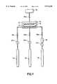
- FIG. 1shows a schematic diagram of a chemical vapor deposition (CVD) apparatus which may be employed in practice of the method of the present invention.
- CVDchemical vapor deposition
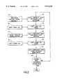
- FIG. 2shows a schematic process flow diagram of the method of the present invention.
- FIG. 3shows a graph of flow rate versus process cycle for a precursor reactant source materials flow, an inert purge gas flow and an oxidant reactant source material flow in accord with the method of the present invention.
- FIG. 4a, FIG.4b and FIG. 4cshow a series of x-ray crystallographic scans as a function of deposition temperature illustrating enhanced crystallinity within a barium strontium titanate (BST) layer when forming the barium strontium titanate (BST) layer in accord with an example of the present invention.
- FIG. 4dshows an x-ray crystallographic scan illustrating attenuated crystallinity within a barium strontium titanate (BST) layer when forming the barium strontium titanate (BST) layer in accord with a continuous chemical vapor deposition (CVD) method generally conventional in the art of multi-component oxide thin film layer deposition.
- CVDchemical vapor deposition
- the present inventionprovides a chemical vapor deposition (CVD) method for forming a multi-component oxide thin film layer over a substrate, such as but not limited to a substrate employed within a thin film microelectronics fabrication or a thin film sensor element fabrication, where the multi-component oxide thin film layer is formed with, amongst other properties, an enhanced crystallinity within the multi-component oxide thin film layer, an enhanced precursor reactant source material incorporation efficiency within the multi-component oxide thin film layer and an enhanced uniformity or conformality of the multi-component oxide thin film layer, at a comparatively low chemical vapor deposition (CVD) substrate temperature.
- CVDchemical vapor deposition
- the method of the present inventionrealizes the foregoing objects by employing when forming a multi-component oxide thin film layer in accord with the present invention a digital chemical vapor deposition (CVD) method through which is first formed a multi-component oxide precursor layer over the substrate, where the multi-component oxide precursor layer is formed through simultaneous introduction of at minimum a first precursor reactant source material and a second precursor reactant source material into a chemical vapor deposition (CVD) reactor chamber in absence of an oxidant reactant source material.
- the multi-component oxide precursor layeris then oxidized within the chemical vapor deposition (CVD) reactor chamber with the oxidant reactant source material in absence of the first precursor reactant source material and the second precursor reactant source material.
- the method of the present inventionmay be employed in forming multi-component oxide thin film layers over substrates employed within thin film fabrications including but not limited to thin film microelectronics fabrications (such as but not limited to integrated circuit thin film microelectronics fabrications, solar cell thin film microelectronics fabrications, ceramic substrate thin film microelectronics fabrications and flat panel display thin film microelectronics fabrications) and thin film sensor element fabrications (such as but not limited to piezoelectric thin film sensor element fabrications, pyroelectric thin film sensor element fabrications, magnetoresistive (MR) thin film sensor element fabrications and chemical gas detector thin film sensor element fabrications).
- thin film microelectronics fabricationssuch as but not limited to integrated circuit thin film microelectronics fabrications, solar cell thin film microelectronics fabrications, ceramic substrate thin film microelectronics fabrications and flat panel display thin film microelectronics fabrications
- thin film sensor element fabricationssuch as but not limited to piezoelectric thin film
- FIG. 1there is shown a schematic diagram of a chemical vapor deposition (CVD) apparatus within which may be formed a multi-component oxide thin film layer in accord with the method of the present invention.
- a chemical vapor deposition (CVD) reactor chamber 10within which there is fixed a platen 12 having positioned thereupon a substrate 14.
- the chemical vapor deposition (CVD) reactor chamber 10 and the platen 12are otherwise conventional in the art of chemical vapor deposition (CVD) methods, but sized appropriately to accommodate the substrate 14.
- the substrate 14may be a substrate employed within a thin film fabrication including but not limited to a thin film microelectronics fabrication or a thin film sensor element fabrication.
- the method of the present inventionhas particular utility in forming high dielectric constant, or ferroelectric, multi-component oxide thin film dielectric layers, such as but not limited to barium strontium titanate (BST) dielectric layers and lead zirconium titanate (PZT) dielectric layers, within advanced integrated circuit thin film microelectronics fabrications such as but not limited to advanced dynamic random access memory (DRAM) integrated circuit thin film microelectronics fabrications, there are many multi-component oxide thin film layers which may be formed through the method of the present invention.
- BSTbarium strontium titanate
- PZTlead zirconium titanate
- the nature of a thin film fabrication into which the substrate 14 is fabricated after the substrate 14 has had a multi-component oxide thin film layer formed over it through the method of the present inventionwill at least in part dictate the nature of a multi-component oxide thin film layer to be formed over the substrate 14.
- the method of the present inventionmay be employed in forming over the substrate 14 multi-component oxide thin film layers including but not limited to barium strontium titanate (BST) multi-component oxide thin film layers, bismuth titanate (BT) multi-component oxide thin film layers, lead zirconium titanate (PZT) multi-component oxide thin film layers, strontium bismuth tantalate (SBT) multi-component oxide thin film layers, strontium bismuth niobate tantalate (SBNT) multi-component oxide thin film layers, calcium, strontium and/or barium doped lanthanum manganese oxide (LMO) based multi-component oxide thin film layers, yttrium barium copper oxide (YBCO) multi-component oxide thin film layers, and bismuth strontium calcium copper oxide (BSCCO) multi-component oxide thin film layers.
- BSTbarium strontium titanate
- BTbismuth titanate
- PZTlead zirconium titanate
- FIG. 1there is also shown in FIG. 1 within the chemical vapor deposition (CVD) reactor chamber 10 a nozzle 16 through which is supplied reactant source materials to the chemical vapor deposition (CVD) reactor chamber 10 in accord with the method of the present invention. Similarly, there is also shown in FIG. 1 connected to the chemical vapor deposition (CVD) reactor chamber 10 a vacuum pump 30 which is employed to evacuate spent reactant source materials from the chemical vapor deposition (CVD) reactor chamber 10, where a spent reactant source material flow may be controlled through use of a chemical vapor deposition (CVD) reactor chamber 10 throttle valve 26d.
- CVDchemical vapor deposition
- FIG. 1connected to and supplying the nozzle 16: (1) a precursor reactant source materials source 18 from which a precursor reactant source materials flow is monitored through a precursor reactant source materials flow meter 24a and controlled through a precursor reactant source materials control valve 26a; (2) an inert purge gas source 20 from which an inert purge gas flow is monitored through an inert purge gas flow meter 24b and controlled through an inert purge gas control valve 26b; and (3) an oxidant reactant source material source 22 from which an oxidant reactant source material flow is monitored through an oxidant reactant source material flow meter 24c and controlled through an oxidant reactant source material control valve 26c.
- a precursor reactant source materials source 18from which a precursor reactant source materials flow is monitored through a precursor reactant source materials flow meter 24a and controlled through a precursor reactant source materials control valve 26a
- an inert purge gas source 20from which an inert purge gas flow is monitored through an inert purge gas flow meter 24b
- an optional flash evaporator 28to be employed when the precursor reactant source materials within the precursor reactant source materials source 18 are in a liquid form which is desired to be vaporized prior to introduction into the chemical vapor deposition (CVD) reactor chamber 10 through the nozzle 16.
- CVDchemical vapor deposition
- the precursor reactant source materials source 18supplies, at minimum, a first precursor reactant source material and a second precursor reactant source material simultaneously to the nozzle 16, and thus to the chemical vapor deposition reactor chamber 10. More preferably, the precursor reactant source materials source 18 simultaneously supplies to the nozzle 16 all of the precursor reactant source materials employed in forming a multi-component oxide layer over the substrate 14 within the chemical vapor deposition (CVD) reactor chamber 10 through the digital chemical vapor deposition (CVD) method of the present invention.
- the number of precursor reactant source materials which might thus more preferably be supplied simultaneously to the nozzle 16 from the precursor reactant source materials source 18may readily be 3, 4, 5 or more precursor reactant source materials.
- the precursor reactant source materialsmay be contained within the precursor reactant source materials source 18 as a mixture of solids, liquids, gases or vapors which do not react substantially to compromise their identity or transport to the nozzle 16 and the chemical vapor deposition (CVD) reactor chamber 10 as individual precursor reactant source materials.
- the precursor reactant source materials within the precursor reactant source materials source 18are in solution.
- the precursor reactant source materials within the precursor reactant source materials source 18are chemically coordinated precursor reactant source materials which provide at minimum a chemically coordinated first precursor reactant source material and a chemically coordinated second precursor reactant source material of sufficient chemical stability and volatility such that their transport to the nozzle 16 and the chemical vapor deposition (CVD) reactor chamber 10 as individual precursor reactant source materials is not compromised.
- at least the first precursor reactant source material and the second precursor reactant source materialmay also be introduced into the chemical vapor deposition (CVD) reactor chamber 10 in conjunction with an inert carrier gas, such as but not limited to helium, neon, argon, xenon or mixtures thereof, in order to secure process optimization.
- a general, but not exclusive, group of chemically coordinated precursor reactant source materials which may be employed as precursor reactant source materials in accord with the method of the present inventionis disclosed within related co-assigned U.S. Pat. No. 5,453,494 to Kirlin et al., the teachings of which are incorporated herein fully by reference.
- Other potential precursor reactant source materials which may be employed within the method of the present inventionare suitable metal oxide precursor materials which are otherwise desirable within conventional continuous chemical vapor deposition (CVD) methods, but undergo facile and undesirable gas phase oxidation reactions with oxidant reactant source materials employed within the method of the present invention.
- the inert purge gas supplied to the chemical vapor deposition (CVD) reactor chamber 10 from the inert purge gas source 20may be selected from the group of inert purge gases including but not limited to helium, neon, argon, xenon and mixtures thereof.
- the oxidant reactant source material supplied to the chemical vapor deposition (CVD) reactor chamber 10 from the oxidant reactant source material source 22may be selected from the group of oxidant reactant source materials consisting of oxygen, ozone, nitrous oxide, nitric oxide, nitrogen dioxide, water vapor, hydrogen peroxide vapor and mixtures thereof, along with suitable non-reactive diluent gases, in order to secure process optimization.
- the oxidant reactant source materialmay be additionally activated through means such as but not limited to plasma activation means, UV light activation means, laser activation means, ion activation means, and/or electron activation means.
- FIG. 2there is shown a schematic process flow diagram illustrating the pertinent process steps through which is formed a multi-component oxide thin film layer in accord with the method of the present invention, while employing the chemical vapor deposition (CVD) apparatus whose schematic cross-sectional diagram is illustrated in FIG. 1.
- CVDchemical vapor deposition
- a multi-component oxide precursor layerover the substrate 14, while employing the precursor reactant source materials obtained from the precursor reactant source materials source 18, where the precursor reactant source materials include at minimum the first precursor reactant source material and the second precursor reactant source material.
- the first precursor reactant source material and the second precursor reactant source materialare simultaneously introduced into the chemical vapor deposition (CVD) reactor chamber 10 in absence of the oxidant reactant source material to form the multi-component oxide precursor layer over the substrate 14.
- the multi-component oxide precursor layeris formed over the substrate 14 to a thickness of from about 5 to about 100 Angstroms employing an appropriate precursor reactant source materials flow rate.
- the chemical vapor deposition (CVD) reactor chamber 10is purged employing the inert purge gas from the inert purge gas source 20.
- the chemical vapor deposition reactor chamber 10is preferably purged with an argon purge gas, preferably at an inert purge gas flow rate which will efficiently purge at minimum the first precursor reactant source material and the second precursor reactant source material from the chemical vapor deposition (CVD) reactor chamber 10.
- an argon purge gaspreferably at an inert purge gas flow rate which will efficiently purge at minimum the first precursor reactant source material and the second precursor reactant source material from the chemical vapor deposition (CVD) reactor chamber 10.
- such a purge ratewill be in the range of from about 50 to about 2000 standard cubic centimeters per minute (sccm).
- the multi-component oxide precursor layeris oxidized, while employing the oxidant reactant source material obtained from the oxidant reactant source material source 22, to form a multi-component oxide layer from the multi-component oxide precursor layer.
- the oxidant reactant source materialis supplied to the chemical vapor deposition (CVD) reactor chamber 10 at a flow rate appropriate to the chemical vapor deposition (CVD) reactor chamber 10 and multi-component oxide precursor layer.
- the oxidant reactant source materialis supplied at a flow rate of from about 50 to about 2000 standard cubic centimeters per minute (sccm).
- the chemical vapor deposition (CVD) reactor chamber 10is purged for a second time, while employing the inert purge gas from the inert purge gas source 20.
- the chemical vapor deposition reactor chamber 10is preferably purged for the second time with the argon purge gas, preferably also at a second inert purge gas flow rate which will efficiently purge the oxidant reactant source material from the chemical vapor deposition (CVD) reactor chamber 10.
- a second purge ratewill also be in the range of from about 50 to about 2000 standard cubic centimeters per minute (sccm).
- the multi-component oxide layer thicknessis measured in-situ. Such measurement is typically and preferably undertaken through optical interferometric measurement methods or x-ray fluorescence methods as are conventional in the art of thin film measurement. If a desired final thickness of the multi-component oxide layer has not been deposited, as illustrated within the decisional process step 42 within the schematic process flow diagram of FIG. 2, the series of process steps 32, 34, 36, 38 and 40 (which in the aggregate form a process cycle) is repeated.
- processing of the substrate 14 in accord with the method of the present inventionis ended and the substrate 14 may then be removed from the chemical vapor deposition (CVD) reactor chamber 10 for appropriate further fabrication.
- CVDchemical vapor deposition
- the multiplicity of process cyclestypically has a range of from about 5 to about 1000 cycles and forms a multi-component oxide layer of thickness from about 20 to about 20000 Angstroms, more preferably from about 50 to about 2000 Angstroms. Under such circumstances, there is assured an optimal oxidation of a multi-component oxide precursor layer when forming the multi-component oxide layer.
- CVDchemical vapor deposition
- additional activation meansbeyond thermal activation means.
- additional activation meansmay include, but are not limited to plasma activation, UV light activation, laser activation, ion activation and/or electron activation.
- FIG. 3there is shown a graph illustrating precursor reactant source materials flow rates, inert purge gas flow rates and oxidant reactant source material flow rates as a function of process cycle, corresponding with the schematic process flow diagram of FIG. 2. Illustrated in FIG. 2 is a pulsed precursor reactant source materials flow rate curve 44, a pulsed inert purge gas flow rate curve 46 and a pulsed oxidant reactant source material flow rate curve 48.
- the pulsed precursor reactant source materials flow rate curve 44typically and preferably has a precursor reactant source materials pulse width PW 1 of from about 2 to about 60 seconds
- the pulsed inert purge gas flow rate curve 46typically and preferably has an inert purge gas pulse width PW2 of from about 0.5 to about 30 seconds
- the pulsed oxidant reactant source material flow rate curve 48typically and preferably has an oxidant reactant source material pulse width PW3 of from about 1 to about 60 seconds.
- the aggregate of a single precursor reactant source materials pulse width PW1 plus a single oxidant reactant source material pulse width PW3 plus two times an inert purge gas pulse width PW2provides a cycle time as illustrated in FIG. 3 of from about 4 to about 180 seconds.
- multi-component oxide thin film layers formed in accord with the method of the present inventionare formed with enhanced crystallinity, enhanced precursor reactant source material incorporation efficiency, and enhanced uniformity, at lower substrate temperatures in comparison with continuous chemical vapor deposition (CVD) methods as are otherwise generally known in the art of thin film deposition.
- CVDchemical vapor deposition
- the method of the present inventionemploys a pulsing of an oxidant reactant source material independent of a pulsing of a group of precursor reactant source materials (along with precursor reactant source materials which are not susceptible to gas phase reactions among themselves), there is attenuated gas phase reactions within reactant source materials when forming a multi-component oxide thin film layer in accord with the method of the present invention.
- the method of the present inventionintroduces simultaneously into a chemical vapor deposition (CVD) reactor chamber at minimum a first precursor reactant source material and a second precursor reactant source material, chemical vapor deposition (CVD) reactor costs associated with introducing the first precursor reactant source material and the second precursor reactant source material into the chemical vapor deposition (CVD) reactor chamber may be reduced.
- CVDchemical vapor deposition
- the two series of substrateswere formed from (100) silicon semiconductor substrates each having formed thereupon a tantalum adhesion layer of thickness about 500 Angstroms deposited through a physical vapor deposition (PVD) method, the tantalum adhesion layer in turn having formed thereupon a platinum layer of thickness about 4000 Angstroms also deposited through a physical vapor deposition (PVD) method.
- PVDphysical vapor deposition
- a barium strontium titanate (BST) multi-component oxide layerthrough a digital chemical vapor deposition (CVD) method in accord with the preferred embodiment of the present invention.
- the digital chemical vapor deposition (CVD) methodemployed: (1) a reactor chamber pressure of about 0.500 torr; (2) a substrate temperature of about 560 degrees Centigrade; (3) a precursor reactant source material mixture comprising the N, N, N', N", N"-pentamethyldiethylenetriamine complexed adducts of: (a) barium bis (2,2,6,6-tetramethyl-3,5-heptanedionate); and (b) strontium bis (2,2,6,6-tetramethyl-3,5-heptanedionate); along with (c) titanium bis (isopropoxide) bis (2,2,6,6-tetramethyl-3,5-heptanedionate) in a 1:1:1.86 molar ratio in an n-buty
- the tetraglyme complexed adducts of barium bis (2,2,6,6-tetramethyl-3,5-heptanedionate) and strontium bis (2,2,6,6-tetramethyl-3,5-heptanedionate)may be substituted for the N, N, N', N", N"-pentamethyldiethylenetriamine complexed adducts of barium bis (2,2,6,6-tetramethyl-3,5-heptanedionate) and strontium bis (2,2,6,6-tetramethyl-3,5-heptanedionate), with equivalent results, provided that the n-butyl acetate/N, N, N', N", N"-pentamethyldiethylenetriamine solvent mixture is substituted with a corresponding n-butyl acetate/tetraglyme solvent mixture.
- the mass flow controllers typically employed in controlling the precursor reactant source materials flash carrier gas flow, the inert purge gas flow and the oxidant reactant source material flow to the chemical vapor deposition (CVD) reactor chamber in accord with the foregoing digital chemical vapor deposition (CVD) methodare known in the art to produce upon actuation a burst of precursor reactant source materials flash carrier gas flow, inert purge gas flow or oxidant reactant source material flow which leads to a transient pressure rise and corresponding increased initial precursor reactant source materials concentration, increased initial inert purge gas concentration or increased initial oxidant reactant source material concentration within the chemical vapor deposition (CVD) reactor chamber.
- barium strontium titanate (BST) layerswere formed upon the first series of substrates employing the foregoing conditions for a total of 100 cycles, which provided barium strontium titanate (BST) layers of total thicknesses about 3300 Angstroms.
- a second series of barium strontium titanate (BST) layerswas formed upon the second series of substrates under deposition conditions otherwise equivalent to the deposition conditions employed within the first series barium strontium titanate (BST) layers, but wherein the precursor reactant source materials and the oxidant reactant source materials were introduced into the chemical vapor deposition (CVD) reactor chamber simultaneously and without separation by a series of argon inert purge gas purge pulses.
- the second series of barium strontium titanate (BST) layerswas formed for continuous deposition times of about 1200 seconds.
- the barium strontium titanate (BST) multi-component oxide thin film layers formed through a digital chemical vapor deposition (CVD) method in accord with the preferred embodiment of the present inventionare formed with enhanced growth rates, and thus correlating enhanced precursor source materials incorporation efficiencies, in comparison with barium strontium titanate (BST) multi-component oxide thin film layers formed through a continuous chemical vapor deposition (CVD) method.
- CVDdigital chemical vapor deposition
- the barium strontium titanate (BST) multi-component oxide thin film layers formed through the digital chemical vapor deposition method in accord with the preferred embodiment of the present inventionare also formed with enhanced dielectric layer properties in comparison with barium strontium titanate (BST) multi-component oxide thin film layers formed through the continuous chemical vapor deposition (CVD) method.
- barium strontium titanate (BST) multi-component oxide thin film layers formed through the digital chemical vapor deposition (CVD) method in accord with the preferred embodiment of the present inventionare also formed with enhanced thickness uniformity, and thus conformality, in comparison with barium strontium titanate (BST) multi-component oxide thin film layers formed through the continuous chemical vapor deposition (CVD) method.
- FIG. 4acorresponds with the x-ray crystallographic diffraction scan for the barium strontium titanate (BST) layer formed through the digital chemical vapor deposition (CVD) method at 560 degrees Centigrade substrate temperature
- FIG. 4bcorresponds with the x-ray crystallographic diffraction scan for the barium strontium titanate (BST) layer formed through the digital chemical vapor deposition (CVD) method at 520 degrees Centigrade substrate temperature
- FIG. 4ccorresponds with the x-ray crystallographic diffraction scan for the barium strontium titanate (BST) layer formed through the digital chemical vapor deposition (CVD) method at 500 degrees Centigrade substrate temperature
- FIG. 4dcorresponds with the x-ray crystallographic diffraction scan for the barium strontium titanate (BST) layer formed through the conventional continuous chemical vapor deposition (CVD) method at 560 degrees Centigrade substrate temperature.
- a corresponding series of crystalline barium strontium titanate (BST) diffraction peaks 50a, 50b, 50c and 50d at a 2 diffraction angle equal to about 57 degreesdecreases in intensity when the digital chemical vapor deposition (CVD) substrate temperature decreases from about 560 degrees Centigrade to about 500 degrees Centigrade and is minimally, if at all, discernibly present within the x-ray diffraction crystallographic scan for the barium strontium titanate (BST) layer formed through the continuous chemical vapor deposition (CVD) method at 560 degrees Centigrade substrate temperature.
- CVDdigital chemical vapor deposition
- multi-component oxide thin film layerssuch as but not limited to barium strontium titanate (BST) multi-component oxide thin layers, with enhanced crystallinity at lower substrate temperatures, in comparison with multi-component oxide thin film layers formed through continuous chemical vapor deposition (CVD) methods.
- BSTbarium strontium titanate
Landscapes
- Chemical & Material Sciences (AREA)
- General Chemical & Material Sciences (AREA)
- Chemical Kinetics & Catalysis (AREA)
- Engineering & Computer Science (AREA)
- Materials Engineering (AREA)
- Mechanical Engineering (AREA)
- Metallurgy (AREA)
- Organic Chemistry (AREA)
- Inorganic Chemistry (AREA)
- Chemical Vapour Deposition (AREA)
Abstract
Description
TABLE I ______________________________________ Exam- BST ple Dep. Method BST Growth Rate (A/second) Dielect. Const. ______________________________________ 1 Digital CVD 2.01 +/- 0.5% (vs precursor only) 231 1.34 +/- 0.5% (vs precursor. & oxidant) 1.04 +/- 0.5% (vs total run time) 2 Continuous CVD 0.60+/- 10% shorted ______________________________________
Claims (24)
Priority Applications (1)
| Application Number | Priority Date | Filing Date | Title |
|---|---|---|---|
| US08/979,465US5972430A (en) | 1997-11-26 | 1997-11-26 | Digital chemical vapor deposition (CVD) method for forming a multi-component oxide layer |
Applications Claiming Priority (1)
| Application Number | Priority Date | Filing Date | Title |
|---|---|---|---|
| US08/979,465US5972430A (en) | 1997-11-26 | 1997-11-26 | Digital chemical vapor deposition (CVD) method for forming a multi-component oxide layer |
Publications (1)
| Publication Number | Publication Date |
|---|---|
| US5972430Atrue US5972430A (en) | 1999-10-26 |
Family
ID=25526904
Family Applications (1)
| Application Number | Title | Priority Date | Filing Date |
|---|---|---|---|
| US08/979,465Expired - LifetimeUS5972430A (en) | 1997-11-26 | 1997-11-26 | Digital chemical vapor deposition (CVD) method for forming a multi-component oxide layer |
Country Status (1)
| Country | Link |
|---|---|
| US (1) | US5972430A (en) |
Cited By (186)
| Publication number | Priority date | Publication date | Assignee | Title |
|---|---|---|---|---|
| US20010054733A1 (en)* | 1999-08-30 | 2001-12-27 | Vishnu Agarwal | Capacitors having a capacitor dielectric layer comprising a metal oxide having multiple different metals bonded with oxygen |
| WO2002007966A1 (en)* | 2000-07-14 | 2002-01-31 | Microcoating Technologies, Inc. | Reduced grain boundary crystalline thin films |
| FR2818993A1 (en)* | 2000-12-28 | 2002-07-05 | Renault | PROCESS FOR DEPOSITING THIN LAYERS ON A POROUS SUBSTRATE, FUEL CELL AND FUEL CELL CONTAINING SUCH THIN LAYER |
| US6478872B1 (en)* | 1999-01-18 | 2002-11-12 | Samsung Electronics Co., Ltd. | Method of delivering gas into reaction chamber and shower head used to deliver gas |
| US20020168553A1 (en)* | 2001-05-07 | 2002-11-14 | Lee Jung-Hyun | Thin film including multi components and method of forming the same |
| US20020180028A1 (en)* | 2001-03-30 | 2002-12-05 | Borovik Alexander S. | Silicon source reagent compositions, and method of making and using same for microelectronic device structure |
| US20020187644A1 (en)* | 2001-03-30 | 2002-12-12 | Baum Thomas H. | Source reagent compositions for CVD formation of gate dielectric thin films using amide precursors and method of using same |
| US20030012875A1 (en)* | 2001-07-10 | 2003-01-16 | Shreyas Kher | CVD BST film composition and property control with thickness below 200 A for DRAM capacitor application with size at 0.1mum or below |
| WO2003012164A1 (en)* | 2001-07-27 | 2003-02-13 | Unaxis Balzers Aktiengesellschaft | Method for the production of coated substrates |
| US20030031793A1 (en)* | 2001-03-20 | 2003-02-13 | Mattson Technology, Inc. | Method for depositing a coating having a relatively high dielectric constant onto a substrate |
| US6551929B1 (en) | 2000-06-28 | 2003-04-22 | Applied Materials, Inc. | Bifurcated deposition process for depositing refractory metal layers employing atomic layer deposition and chemical vapor deposition techniques |
| US20030082296A1 (en)* | 2001-09-14 | 2003-05-01 | Kai Elers | Metal nitride deposition by ALD with reduction pulse |
| US6558517B2 (en) | 2000-05-26 | 2003-05-06 | Micron Technology, Inc. | Physical vapor deposition methods |
| US6566147B2 (en)* | 2001-02-02 | 2003-05-20 | Micron Technology, Inc. | Method for controlling deposition of dielectric films |
| US20030113480A1 (en)* | 2001-12-10 | 2003-06-19 | Hynix Semiconductor Inc. | Method for forming high dielectric layers using atomic layer deposition |
| US6583057B1 (en)* | 1998-12-14 | 2003-06-24 | Motorola, Inc. | Method of forming a semiconductor device having a layer deposited by varying flow of reactants |
| US6599572B2 (en)* | 2000-01-18 | 2003-07-29 | Asm Microchemistry Oy | Process for growing metalloid thin films utilizing boron-containing reducing agents |
| US6599447B2 (en) | 2000-11-29 | 2003-07-29 | Advanced Technology Materials, Inc. | Zirconium-doped BST materials and MOCVD process forming same |
| US6613656B2 (en)* | 2001-02-13 | 2003-09-02 | Micron Technology, Inc. | Sequential pulse deposition |
| US6620723B1 (en) | 2000-06-27 | 2003-09-16 | Applied Materials, Inc. | Formation of boride barrier layers using chemisorption techniques |
| US6620670B2 (en) | 2002-01-18 | 2003-09-16 | Applied Materials, Inc. | Process conditions and precursors for atomic layer deposition (ALD) of AL2O3 |
| US20030172872A1 (en)* | 2002-01-25 | 2003-09-18 | Applied Materials, Inc. | Apparatus for cyclical deposition of thin films |
| US6630201B2 (en) | 2001-04-05 | 2003-10-07 | Angstron Systems, Inc. | Adsorption process for atomic layer deposition |
| US20030198587A1 (en)* | 1999-02-12 | 2003-10-23 | Gelest, Inc. | Method for low-temperature organic chemical vapor deposition of tungsten nitride, tungsten nitride films and tungsten nitride diffusion barriers for computer interconnect metallization |
| US20030203626A1 (en)* | 2002-04-25 | 2003-10-30 | Derderian Garo J. | Apparatus and method for forming thin layers of materials on micro-device workpieces |
| US20030219528A1 (en)* | 2002-05-24 | 2003-11-27 | Carpenter Craig M. | Apparatus and methods for controlling gas pulsing in processes for depositing materials onto micro-device workpieces |
| US6660126B2 (en) | 2001-03-02 | 2003-12-09 | Applied Materials, Inc. | Lid assembly for a processing system to facilitate sequential deposition techniques |
| US20040000270A1 (en)* | 2002-06-26 | 2004-01-01 | Carpenter Craig M. | Methods and apparatus for vapor processing of micro-device workpieces |
| US20040003777A1 (en)* | 2002-07-08 | 2004-01-08 | Carpenter Craig M. | Apparatus and method for depositing materials onto microelectronic workpieces |
| US20040009307A1 (en)* | 2000-06-08 | 2004-01-15 | Won-Yong Koh | Thin film forming method |
| US20040016394A1 (en)* | 2002-07-29 | 2004-01-29 | Castovillo Paul J. | Atomic layer deposition methods |
| US20040025787A1 (en)* | 2002-04-19 | 2004-02-12 | Selbrede Steven C. | System for depositing a film onto a substrate using a low pressure gas precursor |
| US20040033688A1 (en)* | 2002-08-15 | 2004-02-19 | Demetrius Sarigiannis | Atomic layer deposition methods |
| US20040033310A1 (en)* | 2002-08-15 | 2004-02-19 | Demetrius Sarigiannis | Deposition methods |
| US20040038525A1 (en)* | 2002-08-26 | 2004-02-26 | Shuang Meng | Enhanced atomic layer deposition |
| US20040036129A1 (en)* | 2002-08-22 | 2004-02-26 | Micron Technology, Inc. | Atomic layer deposition of CMOS gates with variable work functions |
| US20040065912A1 (en)* | 2002-10-08 | 2004-04-08 | Shangqing Liu | Electrically programmable nonvolatile variable capacitor |
| US20040065253A1 (en)* | 1999-12-03 | 2004-04-08 | Eva Tois | Method of growing oxide thin films |
| US6720027B2 (en) | 2002-04-08 | 2004-04-13 | Applied Materials, Inc. | Cyclical deposition of a variable content titanium silicon nitride layer |
| US6729824B2 (en) | 2001-12-14 | 2004-05-04 | Applied Materials, Inc. | Dual robot processing system |
| US20040083959A1 (en)* | 2001-03-13 | 2004-05-06 | Carpenter Craig M. | Chemical vapor deposition apparatuses and deposition methods |
| US6734020B2 (en) | 2001-03-07 | 2004-05-11 | Applied Materials, Inc. | Valve control system for atomic layer deposition chamber |
| US20040094092A1 (en)* | 2002-02-25 | 2004-05-20 | Derderian Garo J. | Apparatus for improved delivery of metastable species |
| US20040126954A1 (en)* | 2002-08-27 | 2004-07-01 | Eugene Marsh | Deposition methods with time spaced and time abutting precursor pulses |
| US6765178B2 (en) | 2000-12-29 | 2004-07-20 | Applied Materials, Inc. | Chamber for uniform substrate heating |
| JP2004214622A (en)* | 2002-11-14 | 2004-07-29 | Applied Materials Inc | Hybrid chemical treatment apparatus and method |
| US6787186B1 (en)* | 1997-12-18 | 2004-09-07 | Advanced Technology Materials, Inc. | Method of controlled chemical vapor deposition of a metal oxide ceramic layer |
| US20040185177A1 (en)* | 2001-07-13 | 2004-09-23 | Cem Basceri | Chemical vapor deposition methods of forming barium strontium titanate comprising dielectric layers, including such layers having a varied concentration of barium and strontium within the layer |
| US20040185184A1 (en)* | 2002-03-05 | 2004-09-23 | Sandhu Gurtej S. | Atomic layer deposition with point of use generated reactive gas species |
| US6800173B2 (en) | 2000-12-15 | 2004-10-05 | Novellus Systems, Inc. | Variable gas conductance control for a process chamber |
| US6808758B1 (en)* | 2000-06-09 | 2004-10-26 | Mattson Technology, Inc. | Pulse precursor deposition process for forming layers in semiconductor devices |
| US6821563B2 (en) | 2002-10-02 | 2004-11-23 | Applied Materials, Inc. | Gas distribution system for cyclical layer deposition |
| US6825447B2 (en) | 2000-12-29 | 2004-11-30 | Applied Materials, Inc. | Apparatus and method for uniform substrate heating and contaminate collection |
| US6827978B2 (en) | 2002-02-11 | 2004-12-07 | Applied Materials, Inc. | Deposition of tungsten films |
| US20040247787A1 (en)* | 2002-04-19 | 2004-12-09 | Mackie Neil M. | Effluent pressure control for use in a processing system |
| US6833161B2 (en) | 2002-02-26 | 2004-12-21 | Applied Materials, Inc. | Cyclical deposition of tungsten nitride for metal oxide gate electrode |
| US6838122B2 (en)* | 2001-07-13 | 2005-01-04 | Micron Technology, Inc. | Chemical vapor deposition methods of forming barium strontium titanate comprising dielectric layers |
| US6838125B2 (en) | 2002-07-10 | 2005-01-04 | Applied Materials, Inc. | Method of film deposition using activated precursor gases |
| US20050011457A1 (en)* | 2000-12-06 | 2005-01-20 | Chiang Tony P. | Controlling the temperature of a substrate in a film deposition apparatus |
| US6846516B2 (en) | 2002-04-08 | 2005-01-25 | Applied Materials, Inc. | Multiple precursor cyclical deposition system |
| US20050016471A1 (en)* | 2001-04-05 | 2005-01-27 | Chiang Tony P. | Substrate temperature control in an ALD reactor |
| US20050028732A1 (en)* | 2002-01-22 | 2005-02-10 | Mardian Allen P. | Chemical vapor deposition method |
| US20050037154A1 (en)* | 2001-11-08 | 2005-02-17 | Koh Won Yong | Method for forming thin film |
| WO2004105083A3 (en)* | 2003-04-21 | 2005-02-17 | Aviza Tech Inc | System and method for forming multi-component dielectric films |
| US6869838B2 (en) | 2002-04-09 | 2005-03-22 | Applied Materials, Inc. | Deposition of passivation layers for active matrix liquid crystal display (AMLCD) applications |
| US20050070126A1 (en)* | 2003-04-21 | 2005-03-31 | Yoshihide Senzaki | System and method for forming multi-component dielectric films |
| US6875271B2 (en) | 2002-04-09 | 2005-04-05 | Applied Materials, Inc. | Simultaneous cyclical deposition in different processing regions |
| KR100480803B1 (en)* | 2000-12-21 | 2005-04-07 | 주식회사 하이닉스반도체 | Method for fabricating of ferroelectric capacitor |
| US6878206B2 (en) | 2001-07-16 | 2005-04-12 | Applied Materials, Inc. | Lid assembly for a processing system to facilitate sequential deposition techniques |
| US6888188B2 (en) | 2001-08-17 | 2005-05-03 | Micron Technology, Inc. | Capacitor constructions comprising perovskite-type dielectric materials and having different degrees of crystallinity within the perovskite-type dielectric materials |
| US6911391B2 (en) | 2002-01-26 | 2005-06-28 | Applied Materials, Inc. | Integration of titanium and titanium nitride layers |
| US6916398B2 (en) | 2001-10-26 | 2005-07-12 | Applied Materials, Inc. | Gas delivery apparatus and method for atomic layer deposition |
| US20050158448A1 (en)* | 2002-02-25 | 2005-07-21 | Mcneish Allister | Process for coating three-dimensional substrates with thin organic films and products |
| US6936906B2 (en) | 2001-09-26 | 2005-08-30 | Applied Materials, Inc. | Integration of barrier layer and seed layer |
| US20050191416A1 (en)* | 2002-08-15 | 2005-09-01 | Cem Basceri | Methods of gas delivery for deposition processes and methods of depositing material on a substrate |
| US20050212139A1 (en)* | 2004-03-25 | 2005-09-29 | Miika Leinikka | Seed layer formation |
| US6951804B2 (en) | 2001-02-02 | 2005-10-04 | Applied Materials, Inc. | Formation of a tantalum-nitride layer |
| US20050217575A1 (en)* | 2004-03-31 | 2005-10-06 | Dan Gealy | Ampoules for producing a reaction gas and systems for depositing materials onto microfeature workpieces in reaction chambers |
| US20050241763A1 (en)* | 2004-04-30 | 2005-11-03 | Zhisong Huang | Gas distribution system having fast gas switching capabilities |
| US20050271812A1 (en)* | 2004-05-12 | 2005-12-08 | Myo Nyi O | Apparatuses and methods for atomic layer deposition of hafnium-containing high-k dielectric materials |
| US6998014B2 (en) | 2002-01-26 | 2006-02-14 | Applied Materials, Inc. | Apparatus and method for plasma assisted deposition |
| US6998579B2 (en) | 2000-12-29 | 2006-02-14 | Applied Materials, Inc. | Chamber for uniform substrate heating |
| US20060073613A1 (en)* | 2004-09-29 | 2006-04-06 | Sanjeev Aggarwal | Ferroelectric memory cells and methods for fabricating ferroelectric memory cells and ferroelectric capacitors thereof |
| US7049226B2 (en) | 2001-09-26 | 2006-05-23 | Applied Materials, Inc. | Integration of ALD tantalum nitride for copper metallization |
| US7056806B2 (en) | 2003-09-17 | 2006-06-06 | Micron Technology, Inc. | Microfeature workpiece processing apparatus and methods for controlling deposition of materials on microfeature workpieces |
| US7085616B2 (en) | 2001-07-27 | 2006-08-01 | Applied Materials, Inc. | Atomic layer deposition apparatus |
| US7101795B1 (en) | 2000-06-28 | 2006-09-05 | Applied Materials, Inc. | Method and apparatus for depositing refractory metal layers employing sequential deposition techniques to form a nucleation layer |
| US20060201425A1 (en)* | 2005-03-08 | 2006-09-14 | Applied Microstructures, Inc. | Precursor preparation for controlled deposition coatings |
| US7108747B1 (en)* | 1998-09-11 | 2006-09-19 | Asm International N.V. | Method for growing oxide thin films containing barium and strontium |
| US20060213441A1 (en)* | 2003-06-27 | 2006-09-28 | Applied Microstructures, Inc. | Apparatus and method for controlled application of reactive vapors to produce thin films and coatings |
| US20060240542A1 (en)* | 2003-03-12 | 2006-10-26 | Schieve Eric W | Substrate support lift mechanism |
| US20060264066A1 (en)* | 2005-04-07 | 2006-11-23 | Aviza Technology, Inc. | Multilayer multicomponent high-k films and methods for depositing the same |
| US20060292303A1 (en)* | 2005-06-28 | 2006-12-28 | Micron Technology, Inc. | Beta-diketiminate ligand sources and metal-containing compounds thereof, and systems and methods including same |
| WO2007002672A3 (en)* | 2005-06-28 | 2007-02-22 | Micron Technology Inc | Atomic layer deposition using alkaline earth metal beta-diketiminate precursors |
| US20070054048A1 (en)* | 2005-09-07 | 2007-03-08 | Suvi Haukka | Extended deposition range by hot spots |
| US20070066038A1 (en)* | 2004-04-30 | 2007-03-22 | Lam Research Corporation | Fast gas switching plasma processing apparatus |
| US7211144B2 (en) | 2001-07-13 | 2007-05-01 | Applied Materials, Inc. | Pulsed nucleation deposition of tungsten layers |
| US7235138B2 (en) | 2003-08-21 | 2007-06-26 | Micron Technology, Inc. | Microfeature workpiece processing apparatus and methods for batch deposition of materials on microfeature workpieces |
| US7258892B2 (en) | 2003-12-10 | 2007-08-21 | Micron Technology, Inc. | Methods and systems for controlling temperature during microfeature workpiece processing, e.g., CVD deposition |
| US7262133B2 (en) | 2003-01-07 | 2007-08-28 | Applied Materials, Inc. | Enhancement of copper line reliability using thin ALD tan film to cap the copper line |
| US7282239B2 (en) | 2003-09-18 | 2007-10-16 | Micron Technology, Inc. | Systems and methods for depositing material onto microfeature workpieces in reaction chambers |
| US20070287261A1 (en)* | 2001-06-21 | 2007-12-13 | Asm International N.V. | Trench isolation structures for integrated circuits |
| US20080020593A1 (en)* | 2006-07-21 | 2008-01-24 | Wang Chang-Gong | ALD of metal silicate films |
| US7323231B2 (en) | 2003-10-09 | 2008-01-29 | Micron Technology, Inc. | Apparatus and methods for plasma vapor deposition processes |
| US7335396B2 (en) | 2003-04-24 | 2008-02-26 | Micron Technology, Inc. | Methods for controlling mass flow rates and pressures in passageways coupled to reaction chambers and systems for depositing material onto microfeature workpieces in reaction chambers |
| US7342984B1 (en) | 2003-04-03 | 2008-03-11 | Zilog, Inc. | Counting clock cycles over the duration of a first character and using a remainder value to determine when to sample a bit of a second character |
| US7344755B2 (en) | 2003-08-21 | 2008-03-18 | Micron Technology, Inc. | Methods and apparatus for processing microfeature workpieces; methods for conditioning ALD reaction chambers |
| US20080113110A1 (en)* | 2006-10-25 | 2008-05-15 | Asm America, Inc. | Plasma-enhanced deposition of metal carbide films |
| US7402534B2 (en) | 2005-08-26 | 2008-07-22 | Applied Materials, Inc. | Pretreatment processes within a batch ALD reactor |
| US7405158B2 (en) | 2000-06-28 | 2008-07-29 | Applied Materials, Inc. | Methods for depositing tungsten layers employing atomic layer deposition techniques |
| US7416979B2 (en) | 2001-07-25 | 2008-08-26 | Applied Materials, Inc. | Deposition methods for barrier and tungsten materials |
| JP2008199052A (en)* | 2001-05-07 | 2008-08-28 | Samsung Electronics Co Ltd | Multicomponent thin film and method for forming the same |
| US7422635B2 (en) | 2003-08-28 | 2008-09-09 | Micron Technology, Inc. | Methods and apparatus for processing microfeature workpieces, e.g., for depositing materials on microfeature workpieces |
| US7429361B2 (en) | 2002-07-17 | 2008-09-30 | Applied Materials, Inc. | Method and apparatus for providing precursor gas to a processing chamber |
| US20080242111A1 (en)* | 2007-02-15 | 2008-10-02 | Holme Timothy P | Atomic layer deposition of strontium oxide via n-propyltetramethyl cyclopentadiendyl precursor |
| US7439191B2 (en) | 2002-04-05 | 2008-10-21 | Applied Materials, Inc. | Deposition of silicon layers for active matrix liquid crystal display (AMLCD) applications |
| US20080274617A1 (en)* | 2007-05-02 | 2008-11-06 | Asm America, Inc. | Periodic plasma annealing in an ald-type process |
| US7464917B2 (en) | 2005-10-07 | 2008-12-16 | Appiled Materials, Inc. | Ampoule splash guard apparatus |
| US7468104B2 (en) | 2002-05-17 | 2008-12-23 | Micron Technology, Inc. | Chemical vapor deposition apparatus and deposition method |
| US7514358B2 (en) | 2002-03-04 | 2009-04-07 | Applied Materials, Inc. | Sequential deposition of tantalum nitride using a tantalum-containing precursor and a nitrogen-containing precursor |
| US7547952B2 (en) | 2003-04-04 | 2009-06-16 | Applied Materials, Inc. | Method for hafnium nitride deposition |
| US7572731B2 (en) | 2005-06-28 | 2009-08-11 | Micron Technology, Inc. | Unsymmetrical ligand sources, reduced symmetry metal-containing compounds, and systems and methods including same |
| US20090209081A1 (en)* | 2007-12-21 | 2009-08-20 | Asm International N.V. | Silicon Dioxide Thin Films by ALD |
| US7581511B2 (en) | 2003-10-10 | 2009-09-01 | Micron Technology, Inc. | Apparatus and methods for manufacturing microfeatures on workpieces using plasma vapor processes |
| US7582549B2 (en) | 2006-08-25 | 2009-09-01 | Micron Technology, Inc. | Atomic layer deposited barium strontium titanium oxide films |
| US7588804B2 (en) | 2002-08-15 | 2009-09-15 | Micron Technology, Inc. | Reactors with isolated gas connectors and methods for depositing materials onto micro-device workpieces |
| US7595263B2 (en) | 2003-06-18 | 2009-09-29 | Applied Materials, Inc. | Atomic layer deposition of barrier materials |
| US7601648B2 (en) | 2006-07-31 | 2009-10-13 | Applied Materials, Inc. | Method for fabricating an integrated gate dielectric layer for field effect transistors |
| US7611751B2 (en) | 2006-11-01 | 2009-11-03 | Asm America, Inc. | Vapor deposition of metal carbide films |
| US7611990B2 (en) | 2001-07-25 | 2009-11-03 | Applied Materials, Inc. | Deposition methods for barrier and tungsten materials |
| US7615061B2 (en) | 2006-02-28 | 2009-11-10 | Arthrocare Corporation | Bone anchor suture-loading system, method and apparatus |
| US7618681B2 (en) | 2003-10-28 | 2009-11-17 | Asm International N.V. | Process for producing bismuth-containing oxide films |
| US20090305515A1 (en)* | 2008-06-06 | 2009-12-10 | Dustin Ho | Method and apparatus for uv curing with water vapor |
| US7647886B2 (en) | 2003-10-15 | 2010-01-19 | Micron Technology, Inc. | Systems for depositing material onto workpieces in reaction chambers and methods for removing byproducts from reaction chambers |
| US7666474B2 (en) | 2008-05-07 | 2010-02-23 | Asm America, Inc. | Plasma-enhanced pulsed deposition of metal carbide films |
| US7682946B2 (en) | 2005-11-04 | 2010-03-23 | Applied Materials, Inc. | Apparatus and process for plasma-enhanced atomic layer deposition |
| US7699932B2 (en) | 2004-06-02 | 2010-04-20 | Micron Technology, Inc. | Reactors, systems and methods for depositing thin films onto microfeature workpieces |
| US7709402B2 (en) | 2006-02-16 | 2010-05-04 | Micron Technology, Inc. | Conductive layers for hafnium silicon oxynitride films |
| US7732327B2 (en) | 2000-06-28 | 2010-06-08 | Applied Materials, Inc. | Vapor deposition of tungsten materials |
| US7750173B2 (en) | 2007-01-18 | 2010-07-06 | Advanced Technology Materials, Inc. | Tantalum amido-complexes with chelate ligands useful for CVD and ALD of TaN and Ta205 thin films |
| US7775508B2 (en) | 2006-10-31 | 2010-08-17 | Applied Materials, Inc. | Ampoule for liquid draw and vapor draw with a continuous level sensor |
| US7780785B2 (en) | 2001-10-26 | 2010-08-24 | Applied Materials, Inc. | Gas delivery apparatus for atomic layer deposition |
| US7798096B2 (en) | 2006-05-05 | 2010-09-21 | Applied Materials, Inc. | Plasma, UV and ion/neutral assisted ALD or CVD in a batch tool |
| US7867914B2 (en) | 2002-04-16 | 2011-01-11 | Applied Materials, Inc. | System and method for forming an integrated barrier layer |
| US7906393B2 (en) | 2004-01-28 | 2011-03-15 | Micron Technology, Inc. | Methods for forming small-scale capacitor structures |
| US7964505B2 (en) | 2005-01-19 | 2011-06-21 | Applied Materials, Inc. | Atomic layer deposition of tungsten materials |
| US8110489B2 (en) | 2001-07-25 | 2012-02-07 | Applied Materials, Inc. | Process for forming cobalt-containing materials |
| US8119210B2 (en) | 2004-05-21 | 2012-02-21 | Applied Materials, Inc. | Formation of a silicon oxynitride layer on a high-k dielectric material |
| US8133554B2 (en) | 2004-05-06 | 2012-03-13 | Micron Technology, Inc. | Methods for depositing material onto microfeature workpieces in reaction chambers and systems for depositing materials onto microfeature workpieces |
| US8146896B2 (en) | 2008-10-31 | 2012-04-03 | Applied Materials, Inc. | Chemical precursor ampoule for vapor deposition processes |
| US20120127629A1 (en)* | 2009-04-16 | 2012-05-24 | Advanced Technology Materials, Inc. | DOPED ZrO2 CAPACITOR MATERIALS AND STRUCTURES |
| US8187970B2 (en) | 2001-07-25 | 2012-05-29 | Applied Materials, Inc. | Process for forming cobalt and cobalt silicide materials in tungsten contact applications |
| US8323754B2 (en) | 2004-05-21 | 2012-12-04 | Applied Materials, Inc. | Stabilization of high-k dielectric materials |
| US8383525B2 (en) | 2008-04-25 | 2013-02-26 | Asm America, Inc. | Plasma-enhanced deposition process for forming a metal oxide thin film and related structures |
| US20130309417A1 (en)* | 2012-05-16 | 2013-11-21 | Asm Ip Holding B.V. | Methods for forming multi-component thin films |
| US8821637B2 (en) | 2007-01-29 | 2014-09-02 | Applied Materials, Inc. | Temperature controlled lid assembly for tungsten nitride deposition |
| US8841182B1 (en) | 2013-03-14 | 2014-09-23 | Asm Ip Holding B.V. | Silane and borane treatments for titanium carbide films |
| US8846550B1 (en) | 2013-03-14 | 2014-09-30 | Asm Ip Holding B.V. | Silane or borane treatment of metal thin films |
| US8993055B2 (en) | 2005-10-27 | 2015-03-31 | Asm International N.V. | Enhanced thin film deposition |
| US9051641B2 (en) | 2001-07-25 | 2015-06-09 | Applied Materials, Inc. | Cobalt deposition on barrier surfaces |
| US9062390B2 (en) | 2011-09-12 | 2015-06-23 | Asm International N.V. | Crystalline strontium titanate and methods of forming the same |
| US20160071961A1 (en)* | 2014-09-10 | 2016-03-10 | Au Optronics Corporation | Method for fabricating thin film transistor and apparatus thereof |
| US9365926B2 (en) | 2010-02-25 | 2016-06-14 | Asm International N.V. | Precursors and methods for atomic layer deposition of transition metal oxides |
| US9394609B2 (en) | 2014-02-13 | 2016-07-19 | Asm Ip Holding B.V. | Atomic layer deposition of aluminum fluoride thin films |
| US9447496B2 (en) | 2003-02-04 | 2016-09-20 | Asm International N.V. | Nanolayer deposition process |
| US9631272B2 (en) | 2008-04-16 | 2017-04-25 | Asm America, Inc. | Atomic layer deposition of metal carbide films using aluminum hydrocarbon compounds |
| US9704716B2 (en) | 2013-03-13 | 2017-07-11 | Asm Ip Holding B.V. | Deposition of smooth metal nitride films |
| US9708707B2 (en) | 2001-09-10 | 2017-07-18 | Asm International N.V. | Nanolayer deposition using bias power treatment |
| US9786491B2 (en) | 2015-11-12 | 2017-10-10 | Asm Ip Holding B.V. | Formation of SiOCN thin films |
| US9786492B2 (en) | 2015-11-12 | 2017-10-10 | Asm Ip Holding B.V. | Formation of SiOCN thin films |
| US9905414B2 (en) | 2000-09-28 | 2018-02-27 | President And Fellows Of Harvard College | Vapor deposition of metal oxides, silicates and phosphates, and silicon dioxide |
| US9941425B2 (en) | 2015-10-16 | 2018-04-10 | Asm Ip Holdings B.V. | Photoactive devices and materials |
| US10002936B2 (en) | 2014-10-23 | 2018-06-19 | Asm Ip Holding B.V. | Titanium aluminum and tantalum aluminum thin films |
| CN108231957A (en)* | 2017-09-29 | 2018-06-29 | 理想晶延半导体设备(上海)有限公司 | A kind of crystal silicon solar batteries processing method |
| US10186420B2 (en) | 2016-11-29 | 2019-01-22 | Asm Ip Holding B.V. | Formation of silicon-containing thin films |
| US10504901B2 (en) | 2017-04-26 | 2019-12-10 | Asm Ip Holding B.V. | Substrate processing method and device manufactured using the same |
| US10513772B2 (en) | 2009-10-20 | 2019-12-24 | Asm International N.V. | Process for passivating dielectric films |
| US10600637B2 (en) | 2016-05-06 | 2020-03-24 | Asm Ip Holding B.V. | Formation of SiOC thin films |
| US10643925B2 (en) | 2014-04-17 | 2020-05-05 | Asm Ip Holding B.V. | Fluorine-containing conductive films |
| US10847529B2 (en) | 2017-04-13 | 2020-11-24 | Asm Ip Holding B.V. | Substrate processing method and device manufactured by the same |
| US10991573B2 (en) | 2017-12-04 | 2021-04-27 | Asm Ip Holding B.V. | Uniform deposition of SiOC on dielectric and metal surfaces |
| US11158500B2 (en) | 2017-05-05 | 2021-10-26 | Asm Ip Holding B.V. | Plasma enhanced deposition processes for controlled formation of oxygen containing thin films |
| US12142479B2 (en) | 2020-01-17 | 2024-11-12 | Asm Ip Holding B.V. | Formation of SiOCN thin films |
| US12341005B2 (en) | 2020-01-17 | 2025-06-24 | Asm Ip Holding B.V. | Formation of SiCN thin films |
| US12354877B2 (en) | 2020-06-24 | 2025-07-08 | Asm Ip Holding B.V. | Vapor deposition of films comprising molybdenum |
| US12359315B2 (en) | 2019-02-14 | 2025-07-15 | Asm Ip Holding B.V. | Deposition of oxides and nitrides |
Citations (9)
| Publication number | Priority date | Publication date | Assignee | Title |
|---|---|---|---|---|
| US4058430A (en)* | 1974-11-29 | 1977-11-15 | Tuomo Suntola | Method for producing compound thin films |
| US4413022A (en)* | 1979-02-28 | 1983-11-01 | Canon Kabushiki Kaisha | Method for performing growth of compound thin films |
| US5102694A (en)* | 1990-09-27 | 1992-04-07 | Cvd Incorporated | Pulsed chemical vapor deposition of gradient index optical material |
| US5138520A (en)* | 1988-12-27 | 1992-08-11 | Symetrix Corporation | Methods and apparatus for material deposition |
| US5164040A (en)* | 1989-08-21 | 1992-11-17 | Martin Marietta Energy Systems, Inc. | Method and apparatus for rapidly growing films on substrates using pulsed supersonic jets |
| US5330610A (en)* | 1993-05-28 | 1994-07-19 | Martin Marietta Energy Systems, Inc. | Method of digital epilaxy by externally controlled closed-loop feedback |
| US5439876A (en)* | 1988-06-03 | 1995-08-08 | International Business Machines Corporation | Method of making artificial layered high Tc superconductors |
| US5451260A (en)* | 1994-04-15 | 1995-09-19 | Cornell Research Foundation, Inc. | Method and apparatus for CVD using liquid delivery system with an ultrasonic nozzle |
| US5648321A (en)* | 1992-09-11 | 1997-07-15 | International Business Machines Corporation | Process for manufacturing thin films by multi-layer deposition |
- 1997
- 1997-11-26USUS08/979,465patent/US5972430A/ennot_activeExpired - Lifetime
Patent Citations (9)
| Publication number | Priority date | Publication date | Assignee | Title |
|---|---|---|---|---|
| US4058430A (en)* | 1974-11-29 | 1977-11-15 | Tuomo Suntola | Method for producing compound thin films |
| US4413022A (en)* | 1979-02-28 | 1983-11-01 | Canon Kabushiki Kaisha | Method for performing growth of compound thin films |
| US5439876A (en)* | 1988-06-03 | 1995-08-08 | International Business Machines Corporation | Method of making artificial layered high Tc superconductors |
| US5138520A (en)* | 1988-12-27 | 1992-08-11 | Symetrix Corporation | Methods and apparatus for material deposition |
| US5164040A (en)* | 1989-08-21 | 1992-11-17 | Martin Marietta Energy Systems, Inc. | Method and apparatus for rapidly growing films on substrates using pulsed supersonic jets |
| US5102694A (en)* | 1990-09-27 | 1992-04-07 | Cvd Incorporated | Pulsed chemical vapor deposition of gradient index optical material |
| US5648321A (en)* | 1992-09-11 | 1997-07-15 | International Business Machines Corporation | Process for manufacturing thin films by multi-layer deposition |
| US5330610A (en)* | 1993-05-28 | 1994-07-19 | Martin Marietta Energy Systems, Inc. | Method of digital epilaxy by externally controlled closed-loop feedback |
| US5451260A (en)* | 1994-04-15 | 1995-09-19 | Cornell Research Foundation, Inc. | Method and apparatus for CVD using liquid delivery system with an ultrasonic nozzle |
Non-Patent Citations (14)
| Title |
|---|
| Buchholz, et al, "In-Plane Orientation Control of (001) Yba2 Cu3 O7- Grown on (001) MgO by Pulsed Organometallic Beam Epitaxy", Appl. Phys Lett., 68 (21), May 20, 1996, pp. 3037-3039. |
| Buchholz, et al, In Plane Orientation Control of (001) Yba 2 Cu 3 O 7 Grown on (001) MgO by Pulsed Organometallic Beam Epitaxy , Appl. Phys Lett. , 68 (21), May 20, 1996, pp. 3037 3039.* |
| Duray, et al, "Pulsed Organometallic Beam Epitaxy of Complex Oxide Films", Appl. Phys. Lett., 59 (12), Sep. 16, 1991, pp. 1503-1505. |
| Duray, et al, Pulsed Organometallic Beam Epitaxy of Complex Oxide Films , Appl. Phys. Lett. , 59 (12), Sep. 16, 1991, pp. 1503 1505.* |
| Fujii et al, Jpn. J. Appl. Phys. vol. 31 pp. L787 789, Jun. 1992.* |
| Fujii et al, Jpn. J. Appl. Phys. vol. 31 pp. L787-789, Jun. 1992. |
| Hirai, et al, "Preparation of Perovskite Orientated PbZrx Ti1-x O3 Films with Suppressed Vapor Phase Reactions by a Digital Chemical Vapor Deposition Method", Jpn. J. Appl. Phys., vol. 34, Part I, No. 2A, Feb. 1995, pp. 539-543. |
| Hirai, et al, Preparation of Perovskite Orientated PbZr x Ti 1 x O 3 Films with Suppressed Vapor Phase Reactions by a Digital Chemical Vapor Deposition Method , Jpn. J. Appl. Phys. , vol. 34, Part I, No. 2A, Feb. 1995, pp. 539 543.* |
| Ikegawa, et al, "Growth of CeO2 Thin Films by Meal-Organic Molecular Beam Epitaxy", Thin Solids Films, vol. 282, Iss. 1-2, 1996, pp. 60-63. |
| Ikegawa, et al, Growth of CeO 2 Thin Films by Meal Organic Molecular Beam Epitaxy , Thin Solids Films , vol. 282, Iss. 1 2, 1996, pp. 60 63.* |
| Sotome, et al, "C-Axis-Oriented Pb(Zr, Ti)O3 Thin Films Prepared by Digital Metalorganic Chemical Vapor Deposition Method", Jpn. J. Appl. Phys., vol. 33, Part I, No. 7A, Jul. 1994, pp. 4066-4069. |
| Sotome, et al, C Axis Oriented Pb(Zr, Ti)O 3 Thin Films Prepared by Digital Metalorganic Chemical Vapor Deposition Method , Jpn. J. Appl. Phys. , vol. 33, Part I, No. 7A, Jul. 1994, pp. 4066 4069.* |
| Xie, et al, "Epitaxial LiTaO3 The Film by Pulsed Metalorganic Chemical Vapor Deposition from a Single Precursor", Appl. Phys. Lett., 63(23), Dec. 6, 1993, pp. 3146-3148. |
| Xie, et al, Epitaxial LiTaO 3 The Film by Pulsed Metalorganic Chemical Vapor Deposition from a Single Precursor , Appl. Phys. Lett. , 63(23), Dec. 6, 1993, pp. 3146 3148.* |
Cited By (417)
| Publication number | Priority date | Publication date | Assignee | Title |
|---|---|---|---|---|
| US6787186B1 (en)* | 1997-12-18 | 2004-09-07 | Advanced Technology Materials, Inc. | Method of controlled chemical vapor deposition of a metal oxide ceramic layer |
| US7108747B1 (en)* | 1998-09-11 | 2006-09-19 | Asm International N.V. | Method for growing oxide thin films containing barium and strontium |
| US6583057B1 (en)* | 1998-12-14 | 2003-06-24 | Motorola, Inc. | Method of forming a semiconductor device having a layer deposited by varying flow of reactants |
| US6478872B1 (en)* | 1999-01-18 | 2002-11-12 | Samsung Electronics Co., Ltd. | Method of delivering gas into reaction chamber and shower head used to deliver gas |
| US20030198587A1 (en)* | 1999-02-12 | 2003-10-23 | Gelest, Inc. | Method for low-temperature organic chemical vapor deposition of tungsten nitride, tungsten nitride films and tungsten nitride diffusion barriers for computer interconnect metallization |
| US6884466B2 (en) | 1999-02-12 | 2005-04-26 | Gelest, Inc. | Process for low-temperature metal-organic chemical vapor deposition of tungsten nitride and tungsten nitride films |
| US20060006450A1 (en)* | 1999-08-30 | 2006-01-12 | Al-Shareef Husam N | Capacitors having a capacitor dielectric layer comprising a metal oxide having multiple different metals bonded with oxygen |
| US20010054733A1 (en)* | 1999-08-30 | 2001-12-27 | Vishnu Agarwal | Capacitors having a capacitor dielectric layer comprising a metal oxide having multiple different metals bonded with oxygen |
| US20070001206A1 (en)* | 1999-08-30 | 2007-01-04 | Agarwal Vishnu K | Capacitors having a capacitor dielectric layer comprising a metal oxide having multiple different metals bonded with oxygen |
| US6943392B2 (en) | 1999-08-30 | 2005-09-13 | Micron Technology, Inc. | Capacitors having a capacitor dielectric layer comprising a metal oxide having multiple different metals bonded with oxygen |
| US20040065253A1 (en)* | 1999-12-03 | 2004-04-08 | Eva Tois | Method of growing oxide thin films |
| US9514956B2 (en) | 1999-12-03 | 2016-12-06 | Asm International N.V. | Method of growing oxide thin films |
| US20110104906A1 (en)* | 1999-12-03 | 2011-05-05 | Asm International N.V. | Method of growing oxide thin films |
| US7824492B2 (en) | 1999-12-03 | 2010-11-02 | Asm International N.V. | Method of growing oxide thin films |
| US7771533B2 (en) | 1999-12-03 | 2010-08-10 | Asm International N.V. | Atomic-layer-chemical-vapor-deposition of films that contain silicon dioxide |
| US7771534B2 (en) | 1999-12-03 | 2010-08-10 | Asm International N.V. | Method of growing oxide thin films |
| US6599572B2 (en)* | 2000-01-18 | 2003-07-29 | Asm Microchemistry Oy | Process for growing metalloid thin films utilizing boron-containing reducing agents |
| US6794287B2 (en) | 2000-01-18 | 2004-09-21 | Asm International Nv | Process for growing metal or metal carbide thin films utilizing boron-containing reducing agents |
| US7052584B2 (en) | 2000-05-26 | 2006-05-30 | Micron Technology, Inc. | Method of forming a capacitor |
| US20050186688A1 (en)* | 2000-05-26 | 2005-08-25 | Cem Basceri | Chemical vapor deposition methods and physical vapor deposition methods |
| US6884475B2 (en) | 2000-05-26 | 2005-04-26 | Micron Technology, Inc. | Chemical vapor deposition method for depositing a high k dielectric film |
| US20050208219A1 (en)* | 2000-05-26 | 2005-09-22 | Cem Basceri | Method of forming a capacitor |
| US6558517B2 (en) | 2000-05-26 | 2003-05-06 | Micron Technology, Inc. | Physical vapor deposition methods |
| US7217617B2 (en) | 2000-05-26 | 2007-05-15 | Micron Technology, Inc. | Methods of forming a capacitor |
| US20040228968A1 (en)* | 2000-05-26 | 2004-11-18 | Micron Technology, Inc. | Chemical vapor deposition method for depositing a high k dielectric film |
| US7485349B2 (en) | 2000-06-08 | 2009-02-03 | Asm Genitech Korea Ltd. | Thin film forming method |
| US7141278B2 (en) | 2000-06-08 | 2006-11-28 | Asm Genitech Korea Ltd. | Thin film forming method |
| EP1292970B1 (en)* | 2000-06-08 | 2011-09-28 | Genitech Inc. | Thin film forming method |
| US20070048455A1 (en)* | 2000-06-08 | 2007-03-01 | Asm Genitech Korea Ltd. | Thin film forming method |
| EP2293322A1 (en) | 2000-06-08 | 2011-03-09 | Genitech, Inc. | Method for forming a metal nitride layer |
| US20040009307A1 (en)* | 2000-06-08 | 2004-01-15 | Won-Yong Koh | Thin film forming method |
| US6808758B1 (en)* | 2000-06-09 | 2004-10-26 | Mattson Technology, Inc. | Pulse precursor deposition process for forming layers in semiconductor devices |
| US6620723B1 (en) | 2000-06-27 | 2003-09-16 | Applied Materials, Inc. | Formation of boride barrier layers using chemisorption techniques |
| US7501344B2 (en) | 2000-06-27 | 2009-03-10 | Applied Materials, Inc. | Formation of boride barrier layers using chemisorption techniques |
| US7501343B2 (en) | 2000-06-27 | 2009-03-10 | Applied Materials, Inc. | Formation of boride barrier layers using chemisorption techniques |
| US7732327B2 (en) | 2000-06-28 | 2010-06-08 | Applied Materials, Inc. | Vapor deposition of tungsten materials |
| US6551929B1 (en) | 2000-06-28 | 2003-04-22 | Applied Materials, Inc. | Bifurcated deposition process for depositing refractory metal layers employing atomic layer deposition and chemical vapor deposition techniques |
| US7115494B2 (en) | 2000-06-28 | 2006-10-03 | Applied Materials, Inc. | Method and system for controlling the presence of fluorine in refractory metal layers |
| US7465666B2 (en) | 2000-06-28 | 2008-12-16 | Applied Materials, Inc. | Method for forming tungsten materials during vapor deposition processes |
| US7033922B2 (en) | 2000-06-28 | 2006-04-25 | Applied Materials. Inc. | Method and system for controlling the presence of fluorine in refractory metal layers |
| US6855368B1 (en) | 2000-06-28 | 2005-02-15 | Applied Materials, Inc. | Method and system for controlling the presence of fluorine in refractory metal layers |
| US7745333B2 (en) | 2000-06-28 | 2010-06-29 | Applied Materials, Inc. | Methods for depositing tungsten layers employing atomic layer deposition techniques |
| US7101795B1 (en) | 2000-06-28 | 2006-09-05 | Applied Materials, Inc. | Method and apparatus for depositing refractory metal layers employing sequential deposition techniques to form a nucleation layer |
| US7235486B2 (en) | 2000-06-28 | 2007-06-26 | Applied Materials, Inc. | Method for forming tungsten materials during vapor deposition processes |
| US7674715B2 (en) | 2000-06-28 | 2010-03-09 | Applied Materials, Inc. | Method for forming tungsten materials during vapor deposition processes |
| US7846840B2 (en) | 2000-06-28 | 2010-12-07 | Applied Materials, Inc. | Method for forming tungsten materials during vapor deposition processes |
| US7405158B2 (en) | 2000-06-28 | 2008-07-29 | Applied Materials, Inc. | Methods for depositing tungsten layers employing atomic layer deposition techniques |
| WO2002007966A1 (en)* | 2000-07-14 | 2002-01-31 | Microcoating Technologies, Inc. | Reduced grain boundary crystalline thin films |
| US9905414B2 (en) | 2000-09-28 | 2018-02-27 | President And Fellows Of Harvard College | Vapor deposition of metal oxides, silicates and phosphates, and silicon dioxide |
| US6599447B2 (en) | 2000-11-29 | 2003-07-29 | Advanced Technology Materials, Inc. | Zirconium-doped BST materials and MOCVD process forming same |
| US7601393B2 (en) | 2000-12-06 | 2009-10-13 | Novellus Systems, Inc. | Controlling the temperature of a substrate in a film deposition apparatus |
| US20050011457A1 (en)* | 2000-12-06 | 2005-01-20 | Chiang Tony P. | Controlling the temperature of a substrate in a film deposition apparatus |
| US20070184189A1 (en)* | 2000-12-06 | 2007-08-09 | Novellus Systems, Inc. | Controlling the Temperature of a Substrate in a Film Deposition Apparatus |
| US6800173B2 (en) | 2000-12-15 | 2004-10-05 | Novellus Systems, Inc. | Variable gas conductance control for a process chamber |
| US20050051100A1 (en)* | 2000-12-15 | 2005-03-10 | Chiang Tony P. | Variable gas conductance control for a process chamber |
| US7318869B2 (en) | 2000-12-15 | 2008-01-15 | Novellus Systems, Inc. | Variable gas conductance control for a process chamber |
| US7189432B2 (en)* | 2000-12-15 | 2007-03-13 | Novellus Systems, Inc. | Varying conductance out of a process region to control gas flux in an ALD reactor |
| KR100480803B1 (en)* | 2000-12-21 | 2005-04-07 | 주식회사 하이닉스반도체 | Method for fabricating of ferroelectric capacitor |
| WO2002053798A1 (en)* | 2000-12-28 | 2002-07-11 | Renault S.A.S. | Method for depositing thin layers on a porous substrate, fuel cell and fuel cell comprising such a thin layer |
| FR2818993A1 (en)* | 2000-12-28 | 2002-07-05 | Renault | PROCESS FOR DEPOSITING THIN LAYERS ON A POROUS SUBSTRATE, FUEL CELL AND FUEL CELL CONTAINING SUCH THIN LAYER |
| US6825447B2 (en) | 2000-12-29 | 2004-11-30 | Applied Materials, Inc. | Apparatus and method for uniform substrate heating and contaminate collection |
| US7022948B2 (en) | 2000-12-29 | 2006-04-04 | Applied Materials, Inc. | Chamber for uniform substrate heating |
| US6765178B2 (en) | 2000-12-29 | 2004-07-20 | Applied Materials, Inc. | Chamber for uniform substrate heating |
| US6998579B2 (en) | 2000-12-29 | 2006-02-14 | Applied Materials, Inc. | Chamber for uniform substrate heating |
| US9012334B2 (en) | 2001-02-02 | 2015-04-21 | Applied Materials, Inc. | Formation of a tantalum-nitride layer |
| US6838293B2 (en) | 2001-02-02 | 2005-01-04 | Micron Technology, Inc. | Method for controlling deposition of dielectric films |
| US6962824B2 (en) | 2001-02-02 | 2005-11-08 | Micron Technology, Inc. | Method for controlling deposition of dielectric films |
| US7781326B2 (en) | 2001-02-02 | 2010-08-24 | Applied Materials, Inc. | Formation of a tantalum-nitride layer |
| US20050019493A1 (en)* | 2001-02-02 | 2005-01-27 | Micron Technology, Inc. | Method for controlling deposition of dielectric films |
| US6566147B2 (en)* | 2001-02-02 | 2003-05-20 | Micron Technology, Inc. | Method for controlling deposition of dielectric films |
| US6951804B2 (en) | 2001-02-02 | 2005-10-04 | Applied Materials, Inc. | Formation of a tantalum-nitride layer |
| US8114789B2 (en) | 2001-02-02 | 2012-02-14 | Applied Materials, Inc. | Formation of a tantalum-nitride layer |
| US20110212628A1 (en)* | 2001-02-13 | 2011-09-01 | Weimin Li | Sequential pulse deposition |
| US6613656B2 (en)* | 2001-02-13 | 2003-09-02 | Micron Technology, Inc. | Sequential pulse deposition |
| US7910177B2 (en)* | 2001-02-13 | 2011-03-22 | Mosaid Technologies Incorporated | Sequential pulse deposition |
| US20060265100A1 (en)* | 2001-02-13 | 2006-11-23 | Micron Technology, Inc. | Sequential pulse deposition |
| US6660126B2 (en) | 2001-03-02 | 2003-12-09 | Applied Materials, Inc. | Lid assembly for a processing system to facilitate sequential deposition techniques |
| US9587310B2 (en) | 2001-03-02 | 2017-03-07 | Applied Materials, Inc. | Lid assembly for a processing system to facilitate sequential deposition techniques |
| US7201803B2 (en) | 2001-03-07 | 2007-04-10 | Applied Materials, Inc. | Valve control system for atomic layer deposition chamber |
| US6734020B2 (en) | 2001-03-07 | 2004-05-11 | Applied Materials, Inc. | Valve control system for atomic layer deposition chamber |
| US20040216671A1 (en)* | 2001-03-13 | 2004-11-04 | Carpenter Craig M | Chemical vapor deposition apparatuses |
| US7378127B2 (en)* | 2001-03-13 | 2008-05-27 | Micron Technology, Inc. | Chemical vapor deposition methods |
| US20040083959A1 (en)* | 2001-03-13 | 2004-05-06 | Carpenter Craig M. | Chemical vapor deposition apparatuses and deposition methods |
| US20030031793A1 (en)* | 2001-03-20 | 2003-02-13 | Mattson Technology, Inc. | Method for depositing a coating having a relatively high dielectric constant onto a substrate |
| US6884719B2 (en) | 2001-03-20 | 2005-04-26 | Mattson Technology, Inc. | Method for depositing a coating having a relatively high dielectric constant onto a substrate |
| US20020180028A1 (en)* | 2001-03-30 | 2002-12-05 | Borovik Alexander S. | Silicon source reagent compositions, and method of making and using same for microelectronic device structure |
| US6869638B2 (en) | 2001-03-30 | 2005-03-22 | Advanced Tehnology Materials, Inc. | Source reagent compositions for CVD formation of gate dielectric thin films using amide precursors and method of using same |
| US7005392B2 (en) | 2001-03-30 | 2006-02-28 | Advanced Technology Materials, Inc. | Source reagent compositions for CVD formation of gate dielectric thin films using amide precursors and method of using same |
| US20020187644A1 (en)* | 2001-03-30 | 2002-12-12 | Baum Thomas H. | Source reagent compositions for CVD formation of gate dielectric thin films using amide precursors and method of using same |
| US7084080B2 (en) | 2001-03-30 | 2006-08-01 | Advanced Technology Materials, Inc. | Silicon source reagent compositions, and method of making and using same for microelectronic device structure |
| US20060148271A1 (en)* | 2001-03-30 | 2006-07-06 | Borovik Alexander S | Silicon source reagent compositions, and method of making and using same for microelectronic device structure |
| US20060099831A1 (en)* | 2001-03-30 | 2006-05-11 | Borovik Alexander S | Silicon source reagent compositions, and method of making and using same for microelectronic device structure |
| US20050016471A1 (en)* | 2001-04-05 | 2005-01-27 | Chiang Tony P. | Substrate temperature control in an ALD reactor |
| US7806983B2 (en) | 2001-04-05 | 2010-10-05 | Novellus Systems, Inc. | Substrate temperature control in an ALD reactor |
| US6630201B2 (en) | 2001-04-05 | 2003-10-07 | Angstron Systems, Inc. | Adsorption process for atomic layer deposition |
| US20050260348A1 (en)* | 2001-05-07 | 2005-11-24 | Samsung Electronics Co., Ltd. | Thin film including multi components and method of forming the same |
| EP1256638A3 (en)* | 2001-05-07 | 2004-05-06 | Samsung Electronics Co., Ltd. | Thin film including multi components and method of forming the same |
| US20020168553A1 (en)* | 2001-05-07 | 2002-11-14 | Lee Jung-Hyun | Thin film including multi components and method of forming the same |
| JP2008199052A (en)* | 2001-05-07 | 2008-08-28 | Samsung Electronics Co Ltd | Multicomponent thin film and method for forming the same |
| US7709377B2 (en) | 2001-05-07 | 2010-05-04 | Samsung Electronics Co., Ltd. | Thin film including multi components and method of forming the same |
| US20070287261A1 (en)* | 2001-06-21 | 2007-12-13 | Asm International N.V. | Trench isolation structures for integrated circuits |
| WO2003006707A1 (en)* | 2001-07-10 | 2003-01-23 | Applied Materials, Inc. | Method for bst deposition by cvd |
| US20030012875A1 (en)* | 2001-07-10 | 2003-01-16 | Shreyas Kher | CVD BST film composition and property control with thickness below 200 A for DRAM capacitor application with size at 0.1mum or below |
| US7488514B2 (en) | 2001-07-13 | 2009-02-10 | Micron Technology, Inc. | Methods of forming barium strontium titanate layers |
| US6982103B2 (en) | 2001-07-13 | 2006-01-03 | Micron Technology, Inc. | Chemical vapor deposition methods of forming barium strontium titanate comprising dielectric layers, including such layers having a varied concentration of barium and strontium within the layer |
| US7208198B2 (en) | 2001-07-13 | 2007-04-24 | Micron Technology, Inc. | Chemical vapor deposition methods of forming barium strontium titanate comprising dielectric layers, including such layers having a varied concentration of barium and strontium within the layer |
| US20040185177A1 (en)* | 2001-07-13 | 2004-09-23 | Cem Basceri | Chemical vapor deposition methods of forming barium strontium titanate comprising dielectric layers, including such layers having a varied concentration of barium and strontium within the layer |
| US7211144B2 (en) | 2001-07-13 | 2007-05-01 | Applied Materials, Inc. | Pulsed nucleation deposition of tungsten layers |
| US7695563B2 (en) | 2001-07-13 | 2010-04-13 | Applied Materials, Inc. | Pulsed deposition process for tungsten nucleation |
| US20050133127A1 (en)* | 2001-07-13 | 2005-06-23 | Cem Basceri | Methods of forming barium strontium titanate layers |
| US6838122B2 (en)* | 2001-07-13 | 2005-01-04 | Micron Technology, Inc. | Chemical vapor deposition methods of forming barium strontium titanate comprising dielectric layers |
| US20040241322A1 (en)* | 2001-07-13 | 2004-12-02 | Micron Technology, Inc. | Chemical vapor deposition methods of forming barium strontium titanate comprising dielectric layers, including such layers having a varied concentration of barium and strontium within the layer |
| US10280509B2 (en) | 2001-07-16 | 2019-05-07 | Applied Materials, Inc. | Lid assembly for a processing system to facilitate sequential deposition techniques |
| US6878206B2 (en) | 2001-07-16 | 2005-04-12 | Applied Materials, Inc. | Lid assembly for a processing system to facilitate sequential deposition techniques |
| US7905959B2 (en) | 2001-07-16 | 2011-03-15 | Applied Materials, Inc. | Lid assembly for a processing system to facilitate sequential deposition techniques |
| US7416979B2 (en) | 2001-07-25 | 2008-08-26 | Applied Materials, Inc. | Deposition methods for barrier and tungsten materials |
| US9209074B2 (en) | 2001-07-25 | 2015-12-08 | Applied Materials, Inc. | Cobalt deposition on barrier surfaces |
| US9051641B2 (en) | 2001-07-25 | 2015-06-09 | Applied Materials, Inc. | Cobalt deposition on barrier surfaces |
| US8563424B2 (en) | 2001-07-25 | 2013-10-22 | Applied Materials, Inc. | Process for forming cobalt and cobalt silicide materials in tungsten contact applications |
| US8187970B2 (en) | 2001-07-25 | 2012-05-29 | Applied Materials, Inc. | Process for forming cobalt and cobalt silicide materials in tungsten contact applications |
| US8110489B2 (en) | 2001-07-25 | 2012-02-07 | Applied Materials, Inc. | Process for forming cobalt-containing materials |
| US7611990B2 (en) | 2001-07-25 | 2009-11-03 | Applied Materials, Inc. | Deposition methods for barrier and tungsten materials |
| US6835414B2 (en) | 2001-07-27 | 2004-12-28 | Unaxis Balzers Aktiengesellschaft | Method for producing coated substrates |
| WO2003012164A1 (en)* | 2001-07-27 | 2003-02-13 | Unaxis Balzers Aktiengesellschaft | Method for the production of coated substrates |
| US7085616B2 (en) | 2001-07-27 | 2006-08-01 | Applied Materials, Inc. | Atomic layer deposition apparatus |
| US6888188B2 (en) | 2001-08-17 | 2005-05-03 | Micron Technology, Inc. | Capacitor constructions comprising perovskite-type dielectric materials and having different degrees of crystallinity within the perovskite-type dielectric materials |
| US20050191766A1 (en)* | 2001-08-17 | 2005-09-01 | Cem Basceri | Constructions comprising perovskite-type dielectric |
| US6958267B2 (en) | 2001-08-17 | 2005-10-25 | Micron Technology, Inc. | Methods of forming perovskite-type dielectric materials with chemical vapor deposition |
| US7011978B2 (en) | 2001-08-17 | 2006-03-14 | Micron Technology, Inc. | Methods of forming capacitor constructions comprising perovskite-type dielectric materials with different amount of crystallinity regions |
| US7309889B2 (en) | 2001-08-17 | 2007-12-18 | Micron Technology, Inc. | Constructions comprising perovskite-type dielectric |
| US20060246675A1 (en)* | 2001-08-17 | 2006-11-02 | Cem Basceri | Methods of forming capacitor constructions comprising perovskite-type dielectric materials |
| US9708707B2 (en) | 2001-09-10 | 2017-07-18 | Asm International N.V. | Nanolayer deposition using bias power treatment |
| US20060078679A1 (en)* | 2001-09-14 | 2006-04-13 | Kai Elers | Metal nitride carbide deposition by ALD |
| US7410666B2 (en) | 2001-09-14 | 2008-08-12 | Asm International N.V. | Metal nitride carbide deposition by ALD |
| US6986914B2 (en) | 2001-09-14 | 2006-01-17 | Asm International N.V. | Metal nitride deposition by ALD with reduction pulse |
| US20030082296A1 (en)* | 2001-09-14 | 2003-05-01 | Kai Elers | Metal nitride deposition by ALD with reduction pulse |
| US6936906B2 (en) | 2001-09-26 | 2005-08-30 | Applied Materials, Inc. | Integration of barrier layer and seed layer |
| US7049226B2 (en) | 2001-09-26 | 2006-05-23 | Applied Materials, Inc. | Integration of ALD tantalum nitride for copper metallization |
| US7494908B2 (en) | 2001-09-26 | 2009-02-24 | Applied Materials, Inc. | Apparatus for integration of barrier layer and seed layer |
| US7352048B2 (en) | 2001-09-26 | 2008-04-01 | Applied Materials, Inc. | Integration of barrier layer and seed layer |
| US7780788B2 (en) | 2001-10-26 | 2010-08-24 | Applied Materials, Inc. | Gas delivery apparatus for atomic layer deposition |
| US7780785B2 (en) | 2001-10-26 | 2010-08-24 | Applied Materials, Inc. | Gas delivery apparatus for atomic layer deposition |
| US6916398B2 (en) | 2001-10-26 | 2005-07-12 | Applied Materials, Inc. | Gas delivery apparatus and method for atomic layer deposition |
| US8668776B2 (en) | 2001-10-26 | 2014-03-11 | Applied Materials, Inc. | Gas delivery apparatus and method for atomic layer deposition |
| US20050037154A1 (en)* | 2001-11-08 | 2005-02-17 | Koh Won Yong | Method for forming thin film |
| US20030113480A1 (en)* | 2001-12-10 | 2003-06-19 | Hynix Semiconductor Inc. | Method for forming high dielectric layers using atomic layer deposition |
| US6849300B2 (en)* | 2001-12-10 | 2005-02-01 | Hynix Semiconductor, Inc. | Method for forming high dielectric layers using atomic layer deposition |
| US6729824B2 (en) | 2001-12-14 | 2004-05-04 | Applied Materials, Inc. | Dual robot processing system |
| US6620670B2 (en) | 2002-01-18 | 2003-09-16 | Applied Materials, Inc. | Process conditions and precursors for atomic layer deposition (ALD) of AL2O3 |
| US7229666B2 (en) | 2002-01-22 | 2007-06-12 | Micron Technology, Inc. | Chemical vapor deposition method |
| US20050028732A1 (en)* | 2002-01-22 | 2005-02-10 | Mardian Allen P. | Chemical vapor deposition method |
| US8123860B2 (en) | 2002-01-25 | 2012-02-28 | Applied Materials, Inc. | Apparatus for cyclical depositing of thin films |
| US20030172872A1 (en)* | 2002-01-25 | 2003-09-18 | Applied Materials, Inc. | Apparatus for cyclical deposition of thin films |
| US7175713B2 (en) | 2002-01-25 | 2007-02-13 | Applied Materials, Inc. | Apparatus for cyclical deposition of thin films |
| US6998014B2 (en) | 2002-01-26 | 2006-02-14 | Applied Materials, Inc. | Apparatus and method for plasma assisted deposition |
| US7094685B2 (en) | 2002-01-26 | 2006-08-22 | Applied Materials, Inc. | Integration of titanium and titanium nitride layers |
| US6911391B2 (en) | 2002-01-26 | 2005-06-28 | Applied Materials, Inc. | Integration of titanium and titanium nitride layers |
| US7779784B2 (en) | 2002-01-26 | 2010-08-24 | Applied Materials, Inc. | Apparatus and method for plasma assisted deposition |
| US7732325B2 (en) | 2002-01-26 | 2010-06-08 | Applied Materials, Inc. | Plasma-enhanced cyclic layer deposition process for barrier layers |
| US7473638B2 (en) | 2002-01-26 | 2009-01-06 | Applied Materials, Inc. | Plasma-enhanced cyclic layer deposition process for barrier layers |
| US6827978B2 (en) | 2002-02-11 | 2004-12-07 | Applied Materials, Inc. | Deposition of tungsten films |
| US20050158448A1 (en)* | 2002-02-25 | 2005-07-21 | Mcneish Allister | Process for coating three-dimensional substrates with thin organic films and products |
| US20040094092A1 (en)* | 2002-02-25 | 2004-05-20 | Derderian Garo J. | Apparatus for improved delivery of metastable species |
| US7393562B2 (en) | 2002-02-25 | 2008-07-01 | Micron Technology, Inc. | Deposition methods for improved delivery of metastable species |
| US7527693B2 (en) | 2002-02-25 | 2009-05-05 | Micron Technology, Inc. | Apparatus for improved delivery of metastable species |
| US7241478B2 (en) | 2002-02-25 | 2007-07-10 | Bae Systems Information And Electronic Systems Integration Inc. | Process for coating three-dimensional substrates with thin organic films and products |
| US7745329B2 (en) | 2002-02-26 | 2010-06-29 | Applied Materials, Inc. | Tungsten nitride atomic layer deposition processes |
| US6833161B2 (en) | 2002-02-26 | 2004-12-21 | Applied Materials, Inc. | Cyclical deposition of tungsten nitride for metal oxide gate electrode |
| US7115499B2 (en) | 2002-02-26 | 2006-10-03 | Applied Materials, Inc. | Cyclical deposition of tungsten nitride for metal oxide gate electrode |
| US7429516B2 (en) | 2002-02-26 | 2008-09-30 | Applied Materials, Inc. | Tungsten nitride atomic layer deposition processes |
| US7514358B2 (en) | 2002-03-04 | 2009-04-07 | Applied Materials, Inc. | Sequential deposition of tantalum nitride using a tantalum-containing precursor and a nitrogen-containing precursor |
| US7867896B2 (en) | 2002-03-04 | 2011-01-11 | Applied Materials, Inc. | Sequential deposition of tantalum nitride using a tantalum-containing precursor and a nitrogen-containing precursor |
| US7455884B2 (en)* | 2002-03-05 | 2008-11-25 | Micron Technology, Inc. | Atomic layer deposition with point of use generated reactive gas species |
| US20040185184A1 (en)* | 2002-03-05 | 2004-09-23 | Sandhu Gurtej S. | Atomic layer deposition with point of use generated reactive gas species |
| US7439191B2 (en) | 2002-04-05 | 2008-10-21 | Applied Materials, Inc. | Deposition of silicon layers for active matrix liquid crystal display (AMLCD) applications |
| US6846516B2 (en) | 2002-04-08 | 2005-01-25 | Applied Materials, Inc. | Multiple precursor cyclical deposition system |
| US6720027B2 (en) | 2002-04-08 | 2004-04-13 | Applied Materials, Inc. | Cyclical deposition of a variable content titanium silicon nitride layer |
| US7396565B2 (en)* | 2002-04-08 | 2008-07-08 | Applied Materials, Inc. | Multiple precursor cyclical deposition system |
| US6875271B2 (en) | 2002-04-09 | 2005-04-05 | Applied Materials, Inc. | Simultaneous cyclical deposition in different processing regions |
| US6869838B2 (en) | 2002-04-09 | 2005-03-22 | Applied Materials, Inc. | Deposition of passivation layers for active matrix liquid crystal display (AMLCD) applications |
| US7867914B2 (en) | 2002-04-16 | 2011-01-11 | Applied Materials, Inc. | System and method for forming an integrated barrier layer |
| US20040025787A1 (en)* | 2002-04-19 | 2004-02-12 | Selbrede Steven C. | System for depositing a film onto a substrate using a low pressure gas precursor |
| US20040247787A1 (en)* | 2002-04-19 | 2004-12-09 | Mackie Neil M. | Effluent pressure control for use in a processing system |
| US6861094B2 (en)* | 2002-04-25 | 2005-03-01 | Micron Technology, Inc. | Methods for forming thin layers of materials on micro-device workpieces |
| US20030203626A1 (en)* | 2002-04-25 | 2003-10-30 | Derderian Garo J. | Apparatus and method for forming thin layers of materials on micro-device workpieces |
| US20050145337A1 (en)* | 2002-04-25 | 2005-07-07 | Derderian Garo J. | Apparatus for forming thin layers of materials on micro-device workpieces |
| US7468104B2 (en) | 2002-05-17 | 2008-12-23 | Micron Technology, Inc. | Chemical vapor deposition apparatus and deposition method |
| US6838114B2 (en) | 2002-05-24 | 2005-01-04 | Micron Technology, Inc. | Methods for controlling gas pulsing in processes for depositing materials onto micro-device workpieces |
| US20050120954A1 (en)* | 2002-05-24 | 2005-06-09 | Carpenter Craig M. | Apparatus for controlling gas pulsing in processes for depositing materials onto micro-device workpieces |
| US20030219528A1 (en)* | 2002-05-24 | 2003-11-27 | Carpenter Craig M. | Apparatus and methods for controlling gas pulsing in processes for depositing materials onto micro-device workpieces |
| US7481887B2 (en) | 2002-05-24 | 2009-01-27 | Micron Technology, Inc. | Apparatus for controlling gas pulsing in processes for depositing materials onto micro-device workpieces |
| US7118783B2 (en) | 2002-06-26 | 2006-10-10 | Micron Technology, Inc. | Methods and apparatus for vapor processing of micro-device workpieces |
| US20070020394A1 (en)* | 2002-06-26 | 2007-01-25 | Micron Technology, Inc. | Methods and apparatus for vapor processing of micro-device workpieces |
| US20040000270A1 (en)* | 2002-06-26 | 2004-01-01 | Carpenter Craig M. | Methods and apparatus for vapor processing of micro-device workpieces |
| US6821347B2 (en) | 2002-07-08 | 2004-11-23 | Micron Technology, Inc. | Apparatus and method for depositing materials onto microelectronic workpieces |
| US20040003777A1 (en)* | 2002-07-08 | 2004-01-08 | Carpenter Craig M. | Apparatus and method for depositing materials onto microelectronic workpieces |
| US20050133161A1 (en)* | 2002-07-08 | 2005-06-23 | Carpenter Craig M. | Apparatus and method for depositing materials onto microelectronic workpieces |
| US7387685B2 (en) | 2002-07-08 | 2008-06-17 | Micron Technology, Inc. | Apparatus and method for depositing materials onto microelectronic workpieces |
| US6838125B2 (en) | 2002-07-10 | 2005-01-04 | Applied Materials, Inc. | Method of film deposition using activated precursor gases |
| US7678194B2 (en) | 2002-07-17 | 2010-03-16 | Applied Materials, Inc. | Method for providing gas to a processing chamber |
| US7569191B2 (en) | 2002-07-17 | 2009-08-04 | Applied Materials, Inc. | Method and apparatus for providing precursor gas to a processing chamber |
| US7588736B2 (en) | 2002-07-17 | 2009-09-15 | Applied Materials, Inc. | Apparatus and method for generating a chemical precursor |
| US7429361B2 (en) | 2002-07-17 | 2008-09-30 | Applied Materials, Inc. | Method and apparatus for providing precursor gas to a processing chamber |
| WO2004011693A1 (en)* | 2002-07-29 | 2004-02-05 | Micron Technology, Inc. | Atomic deposition layer methods |
| US20050039674A1 (en)* | 2002-07-29 | 2005-02-24 | Castovillo Paul J. | Atomic layer deposition method |
| US7128787B2 (en) | 2002-07-29 | 2006-10-31 | Micron Technology, Inc. | Atomic layer deposition method |
| US7150789B2 (en)* | 2002-07-29 | 2006-12-19 | Micron Technology, Inc. | Atomic layer deposition methods |
| EP1840241A3 (en)* | 2002-07-29 | 2008-11-12 | Micron Technology, Inc. | Atomic deposition layer methods |
| US20040016394A1 (en)* | 2002-07-29 | 2004-01-29 | Castovillo Paul J. | Atomic layer deposition methods |
| US7368382B2 (en) | 2002-08-15 | 2008-05-06 | Micron Technology, Inc. | Atomic layer deposition methods |
| US20060205227A1 (en)* | 2002-08-15 | 2006-09-14 | Demetrius Sarigiannis | Atomic layer deposition methods |
| US20040033688A1 (en)* | 2002-08-15 | 2004-02-19 | Demetrius Sarigiannis | Atomic layer deposition methods |
| US6890596B2 (en) | 2002-08-15 | 2005-05-10 | Micron Technology, Inc. | Deposition methods |
| US7378354B2 (en) | 2002-08-15 | 2008-05-27 | Micron Technology, Inc. | Atomic layer deposition methods |
| US20080241386A1 (en)* | 2002-08-15 | 2008-10-02 | Micron Technology, Inc. | Atomic Layer Deposition Methods |
| US7399499B2 (en) | 2002-08-15 | 2008-07-15 | Micron Technology, Inc. | Methods of gas delivery for deposition processes and methods of depositing material on a substrate |
| US7498057B2 (en) | 2002-08-15 | 2009-03-03 | Micron Technology, Inc. | Deposition methods |
| US6753271B2 (en) | 2002-08-15 | 2004-06-22 | Micron Technology, Inc. | Atomic layer deposition methods |
| US20050147751A1 (en)* | 2002-08-15 | 2005-07-07 | Demetrius Sarigiannis | Deposition methods |
| US20040033310A1 (en)* | 2002-08-15 | 2004-02-19 | Demetrius Sarigiannis | Deposition methods |
| US20050191416A1 (en)* | 2002-08-15 | 2005-09-01 | Cem Basceri | Methods of gas delivery for deposition processes and methods of depositing material on a substrate |
| US7588804B2 (en) | 2002-08-15 | 2009-09-15 | Micron Technology, Inc. | Reactors with isolated gas connectors and methods for depositing materials onto micro-device workpieces |
| US20040224527A1 (en)* | 2002-08-15 | 2004-11-11 | Micron Technology, Inc. | Atomic layer deposition methods |
| US7303991B2 (en) | 2002-08-15 | 2007-12-04 | Micron Technology, Inc. | Atomic layer deposition methods |
| US20040036129A1 (en)* | 2002-08-22 | 2004-02-26 | Micron Technology, Inc. | Atomic layer deposition of CMOS gates with variable work functions |
| US6967154B2 (en) | 2002-08-26 | 2005-11-22 | Micron Technology, Inc. | Enhanced atomic layer deposition |
| US7872291B2 (en) | 2002-08-26 | 2011-01-18 | Round Rock Research, Llc | Enhanced atomic layer deposition |
| US8816447B2 (en) | 2002-08-26 | 2014-08-26 | Round Rock Research, Llc | Transistor with reduced depletion field width |
| US7279732B2 (en) | 2002-08-26 | 2007-10-09 | Micron Technology, Inc. | Enhanced atomic layer deposition |
| US20110108929A1 (en)* | 2002-08-26 | 2011-05-12 | Round Rock Research, Llc | Enhanced atomic layer deposition |
| US8362576B2 (en) | 2002-08-26 | 2013-01-29 | Round Rock Research, Llc | Transistor with reduced depletion field width |
| US20080251828A1 (en)* | 2002-08-26 | 2008-10-16 | Micron Technology, Inc. | Enhanced atomic layer deposition |
| US20040038525A1 (en)* | 2002-08-26 | 2004-02-26 | Shuang Meng | Enhanced atomic layer deposition |
| US20040217410A1 (en)* | 2002-08-26 | 2004-11-04 | Micron Technology, Inc. | Enhanced atomic layer deposition |
| US7271077B2 (en) | 2002-08-27 | 2007-09-18 | Micron Technology, Inc. | Deposition methods with time spaced and time abutting precursor pulses |
| US20040126954A1 (en)* | 2002-08-27 | 2004-07-01 | Eugene Marsh | Deposition methods with time spaced and time abutting precursor pulses |
| US6821563B2 (en) | 2002-10-02 | 2004-11-23 | Applied Materials, Inc. | Gas distribution system for cyclical layer deposition |
| US20040065912A1 (en)* | 2002-10-08 | 2004-04-08 | Shangqing Liu | Electrically programmable nonvolatile variable capacitor |
| US6762481B2 (en)* | 2002-10-08 | 2004-07-13 | The University Of Houston System | Electrically programmable nonvolatile variable capacitor |
| US7402210B2 (en) | 2002-11-14 | 2008-07-22 | Applied Materials, Inc. | Apparatus and method for hybrid chemical processing |
| US20090308318A1 (en)* | 2002-11-14 | 2009-12-17 | Ling Chen | Apparatus and method for hybrid chemical processing |
| EP1420080A3 (en)* | 2002-11-14 | 2005-11-09 | Applied Materials, Inc. | Apparatus and method for hybrid chemical deposition processes |
| US7204886B2 (en) | 2002-11-14 | 2007-04-17 | Applied Materials, Inc. | Apparatus and method for hybrid chemical processing |
| JP2004214622A (en)* | 2002-11-14 | 2004-07-29 | Applied Materials Inc | Hybrid chemical treatment apparatus and method |
| US8070879B2 (en) | 2002-11-14 | 2011-12-06 | Applied Materials, Inc. | Apparatus and method for hybrid chemical processing |
| US7591907B2 (en) | 2002-11-14 | 2009-09-22 | Applied Materials, Inc. | Apparatus for hybrid chemical processing |
| US7262133B2 (en) | 2003-01-07 | 2007-08-28 | Applied Materials, Inc. | Enhancement of copper line reliability using thin ALD tan film to cap the copper line |
| US9447496B2 (en) | 2003-02-04 | 2016-09-20 | Asm International N.V. | Nanolayer deposition process |
| US20060240542A1 (en)* | 2003-03-12 | 2006-10-26 | Schieve Eric W | Substrate support lift mechanism |
| US7871470B2 (en) | 2003-03-12 | 2011-01-18 | Applied Materials, Inc. | Substrate support lift mechanism |
| US7342984B1 (en) | 2003-04-03 | 2008-03-11 | Zilog, Inc. | Counting clock cycles over the duration of a first character and using a remainder value to determine when to sample a bit of a second character |
| US7547952B2 (en) | 2003-04-04 | 2009-06-16 | Applied Materials, Inc. | Method for hafnium nitride deposition |
| US20050064207A1 (en)* | 2003-04-21 | 2005-03-24 | Yoshihide Senzaki | System and method for forming multi-component dielectric films |
| US7470470B2 (en) | 2003-04-21 | 2008-12-30 | Aviza Technology, Inc. | System and method for forming multi-component dielectric films |
| WO2004105083A3 (en)* | 2003-04-21 | 2005-02-17 | Aviza Tech Inc | System and method for forming multi-component dielectric films |
| US20050070126A1 (en)* | 2003-04-21 | 2005-03-31 | Yoshihide Senzaki | System and method for forming multi-component dielectric films |
| US7335396B2 (en) | 2003-04-24 | 2008-02-26 | Micron Technology, Inc. | Methods for controlling mass flow rates and pressures in passageways coupled to reaction chambers and systems for depositing material onto microfeature workpieces in reaction chambers |
| US7595263B2 (en) | 2003-06-18 | 2009-09-29 | Applied Materials, Inc. | Atomic layer deposition of barrier materials |
| US10900123B2 (en)* | 2003-06-27 | 2021-01-26 | Spts Technologies Limited | Apparatus and method for controlled application of reactive vapors to produce thin films and coatings |
| US20060213441A1 (en)* | 2003-06-27 | 2006-09-28 | Applied Microstructures, Inc. | Apparatus and method for controlled application of reactive vapors to produce thin films and coatings |
| US20170335455A1 (en)* | 2003-06-27 | 2017-11-23 | Spts Technologies Ltd. | Apparatus and method for controlled application of reactive vapors to produce thin films and coatings |
| US9725805B2 (en)* | 2003-06-27 | 2017-08-08 | Spts Technologies Limited | Apparatus and method for controlled application of reactive vapors to produce thin films and coatings |
| US7235138B2 (en) | 2003-08-21 | 2007-06-26 | Micron Technology, Inc. | Microfeature workpiece processing apparatus and methods for batch deposition of materials on microfeature workpieces |
| US7344755B2 (en) | 2003-08-21 | 2008-03-18 | Micron Technology, Inc. | Methods and apparatus for processing microfeature workpieces; methods for conditioning ALD reaction chambers |
| US7422635B2 (en) | 2003-08-28 | 2008-09-09 | Micron Technology, Inc. | Methods and apparatus for processing microfeature workpieces, e.g., for depositing materials on microfeature workpieces |
| US7279398B2 (en) | 2003-09-17 | 2007-10-09 | Micron Technology, Inc. | Microfeature workpiece processing apparatus and methods for controlling deposition of materials on microfeature workpieces |
| US7056806B2 (en) | 2003-09-17 | 2006-06-06 | Micron Technology, Inc. | Microfeature workpiece processing apparatus and methods for controlling deposition of materials on microfeature workpieces |
| US7282239B2 (en) | 2003-09-18 | 2007-10-16 | Micron Technology, Inc. | Systems and methods for depositing material onto microfeature workpieces in reaction chambers |
| US7323231B2 (en) | 2003-10-09 | 2008-01-29 | Micron Technology, Inc. | Apparatus and methods for plasma vapor deposition processes |
| US7581511B2 (en) | 2003-10-10 | 2009-09-01 | Micron Technology, Inc. | Apparatus and methods for manufacturing microfeatures on workpieces using plasma vapor processes |
| US7647886B2 (en) | 2003-10-15 | 2010-01-19 | Micron Technology, Inc. | Systems for depositing material onto workpieces in reaction chambers and methods for removing byproducts from reaction chambers |
| US7618681B2 (en) | 2003-10-28 | 2009-11-17 | Asm International N.V. | Process for producing bismuth-containing oxide films |
| US7258892B2 (en) | 2003-12-10 | 2007-08-21 | Micron Technology, Inc. | Methods and systems for controlling temperature during microfeature workpiece processing, e.g., CVD deposition |
| US20100282164A1 (en)* | 2003-12-10 | 2010-11-11 | Micron Technology, Inc. | Methods and systems for controlling temperature during microfeature workpiece processing, e.g., cvd deposition |
| US7771537B2 (en) | 2003-12-10 | 2010-08-10 | Micron Technology, Inc. | Methods and systems for controlling temperature during microfeature workpiece processing, E.G. CVD deposition |
| US8518184B2 (en) | 2003-12-10 | 2013-08-27 | Micron Technology, Inc. | Methods and systems for controlling temperature during microfeature workpiece processing, E.G., CVD deposition |
| US20110163416A1 (en)* | 2004-01-28 | 2011-07-07 | Micron Technology, Inc. | Methods for forming small-scale capacitor structures |
| US7906393B2 (en) | 2004-01-28 | 2011-03-15 | Micron Technology, Inc. | Methods for forming small-scale capacitor structures |
| US8384192B2 (en) | 2004-01-28 | 2013-02-26 | Micron Technology, Inc. | Methods for forming small-scale capacitor structures |
| US20050212139A1 (en)* | 2004-03-25 | 2005-09-29 | Miika Leinikka | Seed layer formation |
| US7405143B2 (en) | 2004-03-25 | 2008-07-29 | Asm International N.V. | Method for fabricating a seed layer |
| US20050217575A1 (en)* | 2004-03-31 | 2005-10-06 | Dan Gealy | Ampoules for producing a reaction gas and systems for depositing materials onto microfeature workpieces in reaction chambers |
| US7584942B2 (en) | 2004-03-31 | 2009-09-08 | Micron Technology, Inc. | Ampoules for producing a reaction gas and systems for depositing materials onto microfeature workpieces in reaction chambers |
| US20050255243A1 (en)* | 2004-04-21 | 2005-11-17 | Aviza Technology, Inc. | System and method for forming multi-component dielectric films |
| US7708859B2 (en) | 2004-04-30 | 2010-05-04 | Lam Research Corporation | Gas distribution system having fast gas switching capabilities |
| US8343876B2 (en) | 2004-04-30 | 2013-01-01 | Lam Research Corporation | Fast gas switching plasma processing apparatus |
| US20070066038A1 (en)* | 2004-04-30 | 2007-03-22 | Lam Research Corporation | Fast gas switching plasma processing apparatus |
| US20050241763A1 (en)* | 2004-04-30 | 2005-11-03 | Zhisong Huang | Gas distribution system having fast gas switching capabilities |
| US20100159707A1 (en)* | 2004-04-30 | 2010-06-24 | Lam Research Corporation | Gas distribution system having fast gas switching capabilities |
| US8673785B2 (en) | 2004-04-30 | 2014-03-18 | Lam Research Corporation | Gas distribution system having fast gas switching capabilities |
| US9023436B2 (en) | 2004-05-06 | 2015-05-05 | Micron Technology, Inc. | Methods for depositing material onto microfeature workpieces in reaction chambers and systems for depositing materials onto microfeature workpieces |
| US8133554B2 (en) | 2004-05-06 | 2012-03-13 | Micron Technology, Inc. | Methods for depositing material onto microfeature workpieces in reaction chambers and systems for depositing materials onto microfeature workpieces |
| US7794544B2 (en) | 2004-05-12 | 2010-09-14 | Applied Materials, Inc. | Control of gas flow and delivery to suppress the formation of particles in an MOCVD/ALD system |
| US8343279B2 (en) | 2004-05-12 | 2013-01-01 | Applied Materials, Inc. | Apparatuses for atomic layer deposition |
| US20050271812A1 (en)* | 2004-05-12 | 2005-12-08 | Myo Nyi O | Apparatuses and methods for atomic layer deposition of hafnium-containing high-k dielectric materials |
| US8282992B2 (en) | 2004-05-12 | 2012-10-09 | Applied Materials, Inc. | Methods for atomic layer deposition of hafnium-containing high-K dielectric materials |
| US8119210B2 (en) | 2004-05-21 | 2012-02-21 | Applied Materials, Inc. | Formation of a silicon oxynitride layer on a high-k dielectric material |
| US8323754B2 (en) | 2004-05-21 | 2012-12-04 | Applied Materials, Inc. | Stabilization of high-k dielectric materials |
| US7699932B2 (en) | 2004-06-02 | 2010-04-20 | Micron Technology, Inc. | Reactors, systems and methods for depositing thin films onto microfeature workpieces |
| US20060073613A1 (en)* | 2004-09-29 | 2006-04-06 | Sanjeev Aggarwal | Ferroelectric memory cells and methods for fabricating ferroelectric memory cells and ferroelectric capacitors thereof |
| US7964505B2 (en) | 2005-01-19 | 2011-06-21 | Applied Materials, Inc. | Atomic layer deposition of tungsten materials |
| US20060201425A1 (en)* | 2005-03-08 | 2006-09-14 | Applied Microstructures, Inc. | Precursor preparation for controlled deposition coatings |
| US7687110B2 (en) | 2005-03-08 | 2010-03-30 | Applied Microstructures, Inc. | Method of in-line purification of CVD reactive precursor materials |
| US20080083329A1 (en)* | 2005-03-08 | 2008-04-10 | Applied Microstructures, Inc. | Method of in-line purification of CVD reactive precursor materials |
| US20060264066A1 (en)* | 2005-04-07 | 2006-11-23 | Aviza Technology, Inc. | Multilayer multicomponent high-k films and methods for depositing the same |
| US7439338B2 (en) | 2005-06-28 | 2008-10-21 | Micron Technology, Inc. | Beta-diketiminate ligand sources and metal-containing compounds thereof, and systems and methods including same |
| US7572731B2 (en) | 2005-06-28 | 2009-08-11 | Micron Technology, Inc. | Unsymmetrical ligand sources, reduced symmetry metal-containing compounds, and systems and methods including same |
| US20060292303A1 (en)* | 2005-06-28 | 2006-12-28 | Micron Technology, Inc. | Beta-diketiminate ligand sources and metal-containing compounds thereof, and systems and methods including same |
| US20080280455A1 (en)* | 2005-06-28 | 2008-11-13 | Micron Technology, Inc. | Atomic layer deposition systems and methods including metal beta-diketiminate compounds |
| US20090075488A1 (en)* | 2005-06-28 | 2009-03-19 | Micron Technology, Inc. | Beta-diketiminate ligand sources and metal-containing compounds thereof, and systems and methods including same |
| US8188464B2 (en) | 2005-06-28 | 2012-05-29 | Micron Technology, Inc. | Atomic layer deposition systems and methods including metal beta-diketiminate compounds |
| US8357784B2 (en) | 2005-06-28 | 2013-01-22 | Micron Technology, Inc. | Beta-diketiminate ligand sources and metal-containing compounds thereof, and systems and methods including same |
| US20110071316A1 (en)* | 2005-06-28 | 2011-03-24 | Micron Technology, Inc. | Unsymmetrical Ligand Sources, Reduced Symmetry Metal-Containing Compounds, and Systems and Methods Including Same |
| US8017184B2 (en) | 2005-06-28 | 2011-09-13 | Micron Technology, Inc. | β-diketiminate ligand sources and metal-containing compounds thereof, and systems and methods including same |
| US7416994B2 (en) | 2005-06-28 | 2008-08-26 | Micron Technology, Inc. | Atomic layer deposition systems and methods including metal beta-diketiminate compounds |
| EP2290126A3 (en)* | 2005-06-28 | 2011-10-12 | Micron Technology, INC. | Atomic layer deposition systems and methods including metal beta-diketiminate compounds |
| US20100186668A1 (en)* | 2005-06-28 | 2010-07-29 | Micron Technology, Inc. | Atomic layer deposition systems and methods including metal beta-diketiminate compounds |
| WO2007002673A3 (en)* | 2005-06-28 | 2007-04-12 | Micron Technology Inc | Beta-diketiminate ligand sources and metal-containing compounds thereof, and systems and methods including same |
| US7858523B2 (en) | 2005-06-28 | 2010-12-28 | Micron Technology, Inc. | Unsymmetrical ligand sources, reduced symmetry metal-containing compounds, and systems and methods including same |
| US20090275199A1 (en)* | 2005-06-28 | 2009-11-05 | Micron Technology, Inc. | Unsymmetrical ligand sources, reduced symmetry metal-containing compounds, and systems and methods including same |
| US7709399B2 (en) | 2005-06-28 | 2010-05-04 | Micron Technology, Inc. | Atomic layer deposition systems and methods including metal β-diketiminate compounds |
| WO2007002672A3 (en)* | 2005-06-28 | 2007-02-22 | Micron Technology Inc | Atomic layer deposition using alkaline earth metal beta-diketiminate precursors |
| US9234273B2 (en) | 2005-06-28 | 2016-01-12 | Micron Technology, Inc. | Unsymmetrical ligand sources, reduced symmetry metal-containing compounds, and systems and methods including same |
| US7402534B2 (en) | 2005-08-26 | 2008-07-22 | Applied Materials, Inc. | Pretreatment processes within a batch ALD reactor |
| US7972978B2 (en) | 2005-08-26 | 2011-07-05 | Applied Materials, Inc. | Pretreatment processes within a batch ALD reactor |
| US20070054048A1 (en)* | 2005-09-07 | 2007-03-08 | Suvi Haukka | Extended deposition range by hot spots |
| US7699295B2 (en) | 2005-10-07 | 2010-04-20 | Applied Materials, Inc. | Ampoule splash guard apparatus |
| US7464917B2 (en) | 2005-10-07 | 2008-12-16 | Appiled Materials, Inc. | Ampoule splash guard apparatus |
| US10297444B2 (en) | 2005-10-27 | 2019-05-21 | Asm International N.V. | Enhanced thin film deposition |
| US9127351B2 (en) | 2005-10-27 | 2015-09-08 | Asm International N.V. | Enhanced thin film deposition |
| US10964534B2 (en) | 2005-10-27 | 2021-03-30 | Asm International | Enhanced thin film deposition |
| US9831094B2 (en) | 2005-10-27 | 2017-11-28 | Asm International N.V. | Enhanced thin film deposition |
| US8993055B2 (en) | 2005-10-27 | 2015-03-31 | Asm International N.V. | Enhanced thin film deposition |
| US9032906B2 (en) | 2005-11-04 | 2015-05-19 | Applied Materials, Inc. | Apparatus and process for plasma-enhanced atomic layer deposition |
| US7850779B2 (en) | 2005-11-04 | 2010-12-14 | Applied Materisals, Inc. | Apparatus and process for plasma-enhanced atomic layer deposition |
| US7682946B2 (en) | 2005-11-04 | 2010-03-23 | Applied Materials, Inc. | Apparatus and process for plasma-enhanced atomic layer deposition |
| US7709402B2 (en) | 2006-02-16 | 2010-05-04 | Micron Technology, Inc. | Conductive layers for hafnium silicon oxynitride films |
| US8067794B2 (en) | 2006-02-16 | 2011-11-29 | Micron Technology, Inc. | Conductive layers for hafnium silicon oxynitride films |
| US8785312B2 (en) | 2006-02-16 | 2014-07-22 | Micron Technology, Inc. | Conductive layers for hafnium silicon oxynitride |
| US7615061B2 (en) | 2006-02-28 | 2009-11-10 | Arthrocare Corporation | Bone anchor suture-loading system, method and apparatus |
| US7798096B2 (en) | 2006-05-05 | 2010-09-21 | Applied Materials, Inc. | Plasma, UV and ion/neutral assisted ALD or CVD in a batch tool |
| US20080020593A1 (en)* | 2006-07-21 | 2008-01-24 | Wang Chang-Gong | ALD of metal silicate films |
| US7795160B2 (en) | 2006-07-21 | 2010-09-14 | Asm America Inc. | ALD of metal silicate films |
| US7601648B2 (en) | 2006-07-31 | 2009-10-13 | Applied Materials, Inc. | Method for fabricating an integrated gate dielectric layer for field effect transistors |
| US7582549B2 (en) | 2006-08-25 | 2009-09-01 | Micron Technology, Inc. | Atomic layer deposited barium strontium titanium oxide films |
| US8581352B2 (en) | 2006-08-25 | 2013-11-12 | Micron Technology, Inc. | Electronic devices including barium strontium titanium oxide films |
| US9202686B2 (en) | 2006-08-25 | 2015-12-01 | Micron Technology, Inc. | Electronic devices including barium strontium titanium oxide films |
| US20080113110A1 (en)* | 2006-10-25 | 2008-05-15 | Asm America, Inc. | Plasma-enhanced deposition of metal carbide films |
| US8268409B2 (en) | 2006-10-25 | 2012-09-18 | Asm America, Inc. | Plasma-enhanced deposition of metal carbide films |
| US7775508B2 (en) | 2006-10-31 | 2010-08-17 | Applied Materials, Inc. | Ampoule for liquid draw and vapor draw with a continuous level sensor |
| US7611751B2 (en) | 2006-11-01 | 2009-11-03 | Asm America, Inc. | Vapor deposition of metal carbide films |
| US20100240918A1 (en)* | 2007-01-18 | 2010-09-23 | Advanced Technology Materials, Inc. | TANTALUM AMIDO-COMPLEXES WITH CHELATE LIGANDS USEFUL FOR CVD AND ALD OF TaN AND Ta205 THIN FILMS |
| US7858816B2 (en) | 2007-01-18 | 2010-12-28 | Advanced Technology Materials, Inc. | Tantalum amido-complexes with chelate ligands useful for CVD and ALD of TaN and Ta205 thin films |
| US7750173B2 (en) | 2007-01-18 | 2010-07-06 | Advanced Technology Materials, Inc. | Tantalum amido-complexes with chelate ligands useful for CVD and ALD of TaN and Ta205 thin films |
| US8821637B2 (en) | 2007-01-29 | 2014-09-02 | Applied Materials, Inc. | Temperature controlled lid assembly for tungsten nitride deposition |
| US20080242111A1 (en)* | 2007-02-15 | 2008-10-02 | Holme Timothy P | Atomic layer deposition of strontium oxide via n-propyltetramethyl cyclopentadiendyl precursor |
| US7790629B2 (en)* | 2007-02-15 | 2010-09-07 | The Board Of Trustees Of The Leland Stanford Junior University | Atomic layer deposition of strontium oxide via N-propyltetramethyl cyclopentadiendyl precursor |
| US20080274617A1 (en)* | 2007-05-02 | 2008-11-06 | Asm America, Inc. | Periodic plasma annealing in an ald-type process |
| US7713874B2 (en) | 2007-05-02 | 2010-05-11 | Asm America, Inc. | Periodic plasma annealing in an ALD-type process |
| US8501637B2 (en) | 2007-12-21 | 2013-08-06 | Asm International N.V. | Silicon dioxide thin films by ALD |
| US20090209081A1 (en)* | 2007-12-21 | 2009-08-20 | Asm International N.V. | Silicon Dioxide Thin Films by ALD |
| US9631272B2 (en) | 2008-04-16 | 2017-04-25 | Asm America, Inc. | Atomic layer deposition of metal carbide films using aluminum hydrocarbon compounds |
| US8383525B2 (en) | 2008-04-25 | 2013-02-26 | Asm America, Inc. | Plasma-enhanced deposition process for forming a metal oxide thin film and related structures |
| US7666474B2 (en) | 2008-05-07 | 2010-02-23 | Asm America, Inc. | Plasma-enhanced pulsed deposition of metal carbide films |
| US20090305515A1 (en)* | 2008-06-06 | 2009-12-10 | Dustin Ho | Method and apparatus for uv curing with water vapor |
| US8146896B2 (en) | 2008-10-31 | 2012-04-03 | Applied Materials, Inc. | Chemical precursor ampoule for vapor deposition processes |
| US20120127629A1 (en)* | 2009-04-16 | 2012-05-24 | Advanced Technology Materials, Inc. | DOPED ZrO2 CAPACITOR MATERIALS AND STRUCTURES |
| US11549177B2 (en) | 2009-10-20 | 2023-01-10 | Asm International, N.V. | Process for passivating dielectric films |
| US10513772B2 (en) | 2009-10-20 | 2019-12-24 | Asm International N.V. | Process for passivating dielectric films |
| US9365926B2 (en) | 2010-02-25 | 2016-06-14 | Asm International N.V. | Precursors and methods for atomic layer deposition of transition metal oxides |
| US11555242B2 (en) | 2010-02-25 | 2023-01-17 | Asm International N.V. | Precursors and methods for atomic layer deposition of transition metal oxides |
| US9677173B2 (en) | 2010-02-25 | 2017-06-13 | Asm International N.V. | Precursors and methods for atomic layer deposition of transition metal oxides |
| US10344378B2 (en) | 2010-02-25 | 2019-07-09 | Asm International N.V. | Precursors and methods for atomic layer deposition of transition metal oxides |
| US9062390B2 (en) | 2011-09-12 | 2015-06-23 | Asm International N.V. | Crystalline strontium titanate and methods of forming the same |
| US9816203B2 (en) | 2011-09-12 | 2017-11-14 | Asm International N.V. | Crystalline strontium titanate and methods of forming the same |
| US9023427B2 (en)* | 2012-05-16 | 2015-05-05 | Asm Ip Holding B.V. | Methods for forming multi-component thin films |
| US20130309417A1 (en)* | 2012-05-16 | 2013-11-21 | Asm Ip Holding B.V. | Methods for forming multi-component thin films |
| US9704716B2 (en) | 2013-03-13 | 2017-07-11 | Asm Ip Holding B.V. | Deposition of smooth metal nitride films |
| US10074541B2 (en) | 2013-03-13 | 2018-09-11 | Asm Ip Holding B.V. | Deposition of smooth metal nitride films |
| US9236247B2 (en) | 2013-03-14 | 2016-01-12 | Asm Ip Holding B.V. | Silane and borane treatments for titanium carbide films |
| US8841182B1 (en) | 2013-03-14 | 2014-09-23 | Asm Ip Holding B.V. | Silane and borane treatments for titanium carbide films |
| US9583348B2 (en) | 2013-03-14 | 2017-02-28 | Asm Ip Holding B.V. | Silane and borane treatments for titanium carbide films |
| US9111749B2 (en) | 2013-03-14 | 2015-08-18 | Asm Ip Holdings B.V. | Silane or borane treatment of metal thin films |
| US8846550B1 (en) | 2013-03-14 | 2014-09-30 | Asm Ip Holding B.V. | Silane or borane treatment of metal thin films |
| US9394609B2 (en) | 2014-02-13 | 2016-07-19 | Asm Ip Holding B.V. | Atomic layer deposition of aluminum fluoride thin films |
| US11450591B2 (en) | 2014-04-17 | 2022-09-20 | Asm Ip Holding B.V. | Fluorine-containing conductive films |
| US11823976B2 (en) | 2014-04-17 | 2023-11-21 | ASM IP Holding, B.V. | Fluorine-containing conductive films |
| US10643925B2 (en) | 2014-04-17 | 2020-05-05 | Asm Ip Holding B.V. | Fluorine-containing conductive films |
| US20160071961A1 (en)* | 2014-09-10 | 2016-03-10 | Au Optronics Corporation | Method for fabricating thin film transistor and apparatus thereof |
| US11139383B2 (en) | 2014-10-23 | 2021-10-05 | Asm Ip Holding B.V. | Titanium aluminum and tantalum aluminum thin films |
| US10002936B2 (en) | 2014-10-23 | 2018-06-19 | Asm Ip Holding B.V. | Titanium aluminum and tantalum aluminum thin films |
| US12237392B2 (en) | 2014-10-23 | 2025-02-25 | Asm Ip Holding B.V. | Titanium aluminum and tantalum aluminum thin films |
| US10636889B2 (en) | 2014-10-23 | 2020-04-28 | Asm Ip Holding B.V. | Titanium aluminum and tantalum aluminum thin films |
| US10861986B2 (en) | 2015-10-16 | 2020-12-08 | Asm Ip Holding B.V. | Photoactive devices and materials |
| US11362222B2 (en) | 2015-10-16 | 2022-06-14 | Asm Ip Holding B.V. | Photoactive devices and materials |
| US9941425B2 (en) | 2015-10-16 | 2018-04-10 | Asm Ip Holdings B.V. | Photoactive devices and materials |
| US9786492B2 (en) | 2015-11-12 | 2017-10-10 | Asm Ip Holding B.V. | Formation of SiOCN thin films |
| US10510529B2 (en) | 2015-11-12 | 2019-12-17 | Asm Ip Holding B.V. | Formation of SiOCN thin films |
| US9786491B2 (en) | 2015-11-12 | 2017-10-10 | Asm Ip Holding B.V. | Formation of SiOCN thin films |
| US11107673B2 (en) | 2015-11-12 | 2021-08-31 | Asm Ip Holding B.V. | Formation of SiOCN thin films |
| US10424476B2 (en) | 2015-11-12 | 2019-09-24 | Asm Ip Holding B.V. | Formation of SiOCN thin films |
| US11996284B2 (en) | 2015-11-12 | 2024-05-28 | Asm Ip Holding B.V. | Formation of SiOCN thin films |
| US11562900B2 (en) | 2016-05-06 | 2023-01-24 | Asm Ip Holding B.V. | Formation of SiOC thin films |
| US10600637B2 (en) | 2016-05-06 | 2020-03-24 | Asm Ip Holding B.V. | Formation of SiOC thin films |
| US12272546B2 (en) | 2016-05-06 | 2025-04-08 | Asm Ip Holding B.V. | Formation of SiOC thin films |
| US10186420B2 (en) | 2016-11-29 | 2019-01-22 | Asm Ip Holding B.V. | Formation of silicon-containing thin films |
| US10847529B2 (en) | 2017-04-13 | 2020-11-24 | Asm Ip Holding B.V. | Substrate processing method and device manufactured by the same |
| US11195845B2 (en) | 2017-04-13 | 2021-12-07 | Asm Ip Holding B.V. | Substrate processing method and device manufactured by the same |
| US10504901B2 (en) | 2017-04-26 | 2019-12-10 | Asm Ip Holding B.V. | Substrate processing method and device manufactured using the same |
| US11776807B2 (en) | 2017-05-05 | 2023-10-03 | ASM IP Holding, B.V. | Plasma enhanced deposition processes for controlled formation of oxygen containing thin films |
| US11158500B2 (en) | 2017-05-05 | 2021-10-26 | Asm Ip Holding B.V. | Plasma enhanced deposition processes for controlled formation of oxygen containing thin films |
| CN108231957A (en)* | 2017-09-29 | 2018-06-29 | 理想晶延半导体设备(上海)有限公司 | A kind of crystal silicon solar batteries processing method |
| US10991573B2 (en) | 2017-12-04 | 2021-04-27 | Asm Ip Holding B.V. | Uniform deposition of SiOC on dielectric and metal surfaces |
| US12359315B2 (en) | 2019-02-14 | 2025-07-15 | Asm Ip Holding B.V. | Deposition of oxides and nitrides |
| US12142479B2 (en) | 2020-01-17 | 2024-11-12 | Asm Ip Holding B.V. | Formation of SiOCN thin films |
| US12341005B2 (en) | 2020-01-17 | 2025-06-24 | Asm Ip Holding B.V. | Formation of SiCN thin films |
| US12354877B2 (en) | 2020-06-24 | 2025-07-08 | Asm Ip Holding B.V. | Vapor deposition of films comprising molybdenum |
Similar Documents
| Publication | Publication Date | Title |
|---|---|---|
| US5972430A (en) | Digital chemical vapor deposition (CVD) method for forming a multi-component oxide layer | |
| US5138520A (en) | Methods and apparatus for material deposition | |
| US5527567A (en) | Metalorganic chemical vapor deposition of layered structure oxides | |
| US5478610A (en) | Metalorganic chemical vapor deposition of layered structure oxides | |
| US5431958A (en) | Metalorganic chemical vapor deposition of ferroelectric thin films | |
| US9117773B2 (en) | High concentration water pulses for atomic layer deposition | |
| EP1292970B1 (en) | Thin film forming method | |
| US5104690A (en) | CVD thin film compounds | |
| EP1433874A2 (en) | Method for metal oxide thin film deposition via MOCVD | |
| US20080072819A1 (en) | Metal oxide films | |
| JPH0790587A (en) | Method of manufacturing ferroelectric thin film | |
| US20060088660A1 (en) | Methods of depositing lead containing oxides films | |
| US20070287248A1 (en) | Method for manufacturing capacity element, method for manufacturing semiconductor device and semiconductor-manufacturing apparatus | |
| JP3032416B2 (en) | CVD thin film forming method | |
| KR100876474B1 (en) | Deposition Method and Deposition Device | |
| Nukaga et al. | Effect of deposition temperature and composition on the microstructure and electrical property of SrBi2Ta2O9 thin films prepared by metalorganic chemical vapor deposition | |
| KR100445625B1 (en) | Method of Making Bismuth Compound and Dielectric Material of Bismuth | |
| JP3224293B2 (en) | Manufacturing method of dielectric thin film | |
| EP1662556A1 (en) | Process for producing oxide thin film and production apparatus therefor | |
| KR100229358B1 (en) | SBT ferroelectric thin film manufacturing method | |
| US6686210B1 (en) | Methods for controlling the crystallographic texture of thin films with anisotropic ferroelectric polarization or permittivity | |
| CN1060224C (en) | Forming method for lead phthalic and lanthanum phthalic film | |
| AU636818B2 (en) | Methods and apparatus for material deposition | |
| EP1734151A1 (en) | A method and system for metalorganic chemical vapour deposition (MOCVD) and annealing of lead germanite (PGO) thin films films | |
| US7250228B2 (en) | Yttrium-doped bismuth titanate thin film and preparation thereof |
Legal Events
| Date | Code | Title | Description |
|---|---|---|---|
| AS | Assignment | Owner name:ADVANCED TECHNOLOGY MATERIALS, INC., CONNECTICUT Free format text:ASSIGNMENT OF ASSIGNORS INTEREST;ASSIGNORS:BILODEAU, STEVEN M.;VAN BUSKIRK, PETER C.;DIMEO, FRANK, JR.;REEL/FRAME:009108/0743 Effective date:19971125 | |
| STCF | Information on status: patent grant | Free format text:PATENTED CASE | |
| CC | Certificate of correction | ||
| FEPP | Fee payment procedure | Free format text:PAT HOLDER NO LONGER CLAIMS SMALL ENTITY STATUS, ENTITY STATUS SET TO UNDISCOUNTED (ORIGINAL EVENT CODE: STOL); ENTITY STATUS OF PATENT OWNER: LARGE ENTITY | |
| FPAY | Fee payment | Year of fee payment:4 | |
| CC | Certificate of correction | ||
| FPAY | Fee payment | Year of fee payment:8 | |
| FEPP | Fee payment procedure | Free format text:PAYOR NUMBER ASSIGNED (ORIGINAL EVENT CODE: ASPN); ENTITY STATUS OF PATENT OWNER: LARGE ENTITY | |
| FPAY | Fee payment | Year of fee payment:12 | |
| AS | Assignment | Owner name:GOLDMAN SACHS BANK USA, AS COLLATERAL AGENT, NEW YORK Free format text:SECURITY INTEREST;ASSIGNORS:ENTEGRIS, INC.;POCO GRAPHITE, INC.;ATMI, INC.;AND OTHERS;REEL/FRAME:032815/0852 Effective date:20140430 Owner name:GOLDMAN SACHS BANK USA, AS COLLATERAL AGENT, NEW Y Free format text:SECURITY INTEREST;ASSIGNORS:ENTEGRIS, INC.;POCO GRAPHITE, INC.;ATMI, INC.;AND OTHERS;REEL/FRAME:032815/0852 Effective date:20140430 | |
| AS | Assignment | Owner name:GOLDMAN SACHS BANK USA, AS COLLATERAL AGENT, NEW YORK Free format text:SECURITY INTEREST;ASSIGNORS:ENTEGRIS, INC.;POCO GRAPHITE, INC.;ATMI, INC.;AND OTHERS;REEL/FRAME:032812/0192 Effective date:20140430 Owner name:GOLDMAN SACHS BANK USA, AS COLLATERAL AGENT, NEW Y Free format text:SECURITY INTEREST;ASSIGNORS:ENTEGRIS, INC.;POCO GRAPHITE, INC.;ATMI, INC.;AND OTHERS;REEL/FRAME:032812/0192 Effective date:20140430 | |
| AS | Assignment | Owner name:ENTEGRIS, INC., MASSACHUSETTS Free format text:ASSIGNMENT OF ASSIGNORS INTEREST;ASSIGNOR:ADVANCED TECHNOLOGY MATERIALS, INC.;REEL/FRAME:034894/0025 Effective date:20150204 | |
| AS | Assignment | Owner name:ATMI PACKAGING, INC., CONNECTICUT Free format text:RELEASE BY SECURED PARTY;ASSIGNOR:GOLDMAN SACHS BANK USA, AS COLLATERAL AGENT;REEL/FRAME:047477/0032 Effective date:20181106 Owner name:ATMI, INC., CONNECTICUT Free format text:RELEASE BY SECURED PARTY;ASSIGNOR:GOLDMAN SACHS BANK USA, AS COLLATERAL AGENT;REEL/FRAME:047477/0032 Effective date:20181106 Owner name:ADVANCED TECHNOLOGY MATERIALS, INC., CONNECTICUT Free format text:RELEASE BY SECURED PARTY;ASSIGNOR:GOLDMAN SACHS BANK USA, AS COLLATERAL AGENT;REEL/FRAME:047477/0032 Effective date:20181106 Owner name:ENTEGRIS, INC., MASSACHUSETTS Free format text:RELEASE BY SECURED PARTY;ASSIGNOR:GOLDMAN SACHS BANK USA, AS COLLATERAL AGENT;REEL/FRAME:047477/0032 Effective date:20181106 Owner name:POCO GRAPHITE, INC., MASSACHUSETTS Free format text:RELEASE BY SECURED PARTY;ASSIGNOR:GOLDMAN SACHS BANK USA, AS COLLATERAL AGENT;REEL/FRAME:047477/0032 Effective date:20181106 Owner name:ENTEGRIS, INC., MASSACHUSETTS Free format text:RELEASE BY SECURED PARTY;ASSIGNOR:GOLDMAN SACHS BANK USA, AS COLLATERAL AGENT;REEL/FRAME:047477/0151 Effective date:20181106 Owner name:POCO GRAPHITE, INC., MASSACHUSETTS Free format text:RELEASE BY SECURED PARTY;ASSIGNOR:GOLDMAN SACHS BANK USA, AS COLLATERAL AGENT;REEL/FRAME:047477/0151 Effective date:20181106 Owner name:ATMI PACKAGING, INC., CONNECTICUT Free format text:RELEASE BY SECURED PARTY;ASSIGNOR:GOLDMAN SACHS BANK USA, AS COLLATERAL AGENT;REEL/FRAME:047477/0151 Effective date:20181106 Owner name:ADVANCED TECHNOLOGY MATERIALS, INC., CONNECTICUT Free format text:RELEASE BY SECURED PARTY;ASSIGNOR:GOLDMAN SACHS BANK USA, AS COLLATERAL AGENT;REEL/FRAME:047477/0151 Effective date:20181106 Owner name:ATMI, INC., CONNECTICUT Free format text:RELEASE BY SECURED PARTY;ASSIGNOR:GOLDMAN SACHS BANK USA, AS COLLATERAL AGENT;REEL/FRAME:047477/0151 Effective date:20181106 |