US5972179A - Silicon IC contacts using composite TiN barrier layer - Google Patents
Silicon IC contacts using composite TiN barrier layerDownload PDFInfo
- Publication number
- US5972179A US5972179AUS08/941,556US94155697AUS5972179AUS 5972179 AUS5972179 AUS 5972179AUS 94155697 AUS94155697 AUS 94155697AUS 5972179 AUS5972179 AUS 5972179A
- Authority
- US
- United States
- Prior art keywords
- layer
- tin
- cvd
- deposited
- silicon
- Prior art date
- Legal status (The legal status is an assumption and is not a legal conclusion. Google has not performed a legal analysis and makes no representation as to the accuracy of the status listed.)
- Expired - Lifetime
Links
- ATJFFYVFTNAWJD-UHFFFAOYSA-NTinChemical compound[Sn]ATJFFYVFTNAWJD-UHFFFAOYSA-N0.000titleclaimsabstractdescription40
- 229910052710siliconInorganic materials0.000titleclaimsdescription20
- XUIMIQQOPSSXEZ-UHFFFAOYSA-NSiliconChemical compound[Si]XUIMIQQOPSSXEZ-UHFFFAOYSA-N0.000titleclaimsdescription18
- 239000010703siliconSubstances0.000titleclaimsdescription18
- 230000004888barrier functionEffects0.000titleabstractdescription23
- 239000002131composite materialSubstances0.000titleabstractdescription4
- 238000000151depositionMethods0.000claimsabstractdescription27
- 230000008021depositionEffects0.000claimsabstractdescription15
- 229910000838Al alloyInorganic materials0.000claimsabstractdescription13
- 238000000034methodMethods0.000claimsdescription31
- 238000005229chemical vapour depositionMethods0.000claimsdescription21
- 239000010936titaniumSubstances0.000claimsdescription20
- 230000008569processEffects0.000claimsdescription19
- RTAQQCXQSZGOHL-UHFFFAOYSA-NTitaniumChemical compound[Ti]RTAQQCXQSZGOHL-UHFFFAOYSA-N0.000claimsdescription9
- 238000004544sputter depositionMethods0.000claimsdescription9
- 229910052719titaniumInorganic materials0.000claimsdescription9
- IJGRMHOSHXDMSA-UHFFFAOYSA-NAtomic nitrogenChemical compoundN#NIJGRMHOSHXDMSA-UHFFFAOYSA-N0.000claimsdescription8
- 229910052782aluminiumInorganic materials0.000claimsdescription7
- XAGFODPZIPBFFR-UHFFFAOYSA-NaluminiumChemical compound[Al]XAGFODPZIPBFFR-UHFFFAOYSA-N0.000claimsdescription7
- MNWRORMXBIWXCI-UHFFFAOYSA-Ntetrakis(dimethylamido)titaniumChemical compoundCN(C)[Ti](N(C)C)(N(C)C)N(C)CMNWRORMXBIWXCI-UHFFFAOYSA-N0.000claimsdescription7
- 239000002243precursorSubstances0.000claimsdescription5
- 229910052757nitrogenInorganic materials0.000claimsdescription4
- QVGXLLKOCUKJST-UHFFFAOYSA-Natomic oxygenChemical compound[O]QVGXLLKOCUKJST-UHFFFAOYSA-N0.000claimsdescription3
- 239000001301oxygenSubstances0.000claimsdescription3
- 229910052760oxygenInorganic materials0.000claimsdescription3
- 238000004519manufacturing processMethods0.000claims1
- 239000000463materialSubstances0.000description10
- 238000005240physical vapour depositionMethods0.000description10
- 239000000758substrateSubstances0.000description7
- XKRFYHLGVUSROY-UHFFFAOYSA-NArgonChemical compound[Ar]XKRFYHLGVUSROY-UHFFFAOYSA-N0.000description6
- 239000013078crystalSubstances0.000description4
- 238000001465metallisationMethods0.000description4
- 238000009832plasma treatmentMethods0.000description4
- 229910021420polycrystalline siliconInorganic materials0.000description4
- 229920005591polysiliconPolymers0.000description4
- 229910003074TiCl4Inorganic materials0.000description3
- 229910045601alloyInorganic materials0.000description3
- 239000000956alloySubstances0.000description3
- 238000013459approachMethods0.000description3
- 229910052786argonInorganic materials0.000description3
- 239000012535impuritySubstances0.000description3
- 238000012545processingMethods0.000description3
- XJDNKRIXUMDJCW-UHFFFAOYSA-Jtitanium tetrachlorideChemical compoundCl[Ti](Cl)(Cl)ClXJDNKRIXUMDJCW-UHFFFAOYSA-J0.000description3
- 230000009466transformationEffects0.000description3
- OKTJSMMVPCPJKN-UHFFFAOYSA-NCarbonChemical compound[C]OKTJSMMVPCPJKN-UHFFFAOYSA-N0.000description2
- NRTOMJZYCJJWKI-UHFFFAOYSA-NTitanium nitrideChemical compound[Ti]#NNRTOMJZYCJJWKI-UHFFFAOYSA-N0.000description2
- 230000015572biosynthetic processEffects0.000description2
- 229910052799carbonInorganic materials0.000description2
- 238000006243chemical reactionMethods0.000description2
- 239000000460chlorineSubstances0.000description2
- 238000000576coating methodMethods0.000description2
- 238000002425crystallisationMethods0.000description2
- 230000008025crystallizationEffects0.000description2
- 230000001788irregularEffects0.000description2
- NJPPVKZQTLUDBO-UHFFFAOYSA-NnovaluronChemical compoundC1=C(Cl)C(OC(F)(F)C(OC(F)(F)F)F)=CC=C1NC(=O)NC(=O)C1=C(F)C=CC=C1FNJPPVKZQTLUDBO-UHFFFAOYSA-N0.000description2
- 238000002161passivationMethods0.000description2
- 238000011160researchMethods0.000description2
- 238000012421spikingMethods0.000description2
- 229910018125Al-SiInorganic materials0.000description1
- 229910018520Al—SiInorganic materials0.000description1
- ZAMOUSCENKQFHK-UHFFFAOYSA-NChlorine atomChemical compound[Cl]ZAMOUSCENKQFHK-UHFFFAOYSA-N0.000description1
- 229910000881Cu alloyInorganic materials0.000description1
- UFHFLCQGNIYNRP-UHFFFAOYSA-NHydrogenChemical compound[H][H]UFHFLCQGNIYNRP-UHFFFAOYSA-N0.000description1
- 229910018594Si-CuInorganic materials0.000description1
- 229910008465Si—CuInorganic materials0.000description1
- 238000005275alloyingMethods0.000description1
- 238000000637aluminium metallisationMethods0.000description1
- 125000003277amino groupChemical group0.000description1
- 238000000137annealingMethods0.000description1
- 230000000740bleeding effectEffects0.000description1
- 239000012159carrier gasSubstances0.000description1
- 229910052801chlorineInorganic materials0.000description1
- 239000011248coating agentSubstances0.000description1
- 239000002178crystalline materialSubstances0.000description1
- 238000013461designMethods0.000description1
- VJDVOZLYDLHLSM-UHFFFAOYSA-Ndiethylazanide;titanium(4+)Chemical compound[Ti+4].CC[N-]CC.CC[N-]CC.CC[N-]CC.CC[N-]CCVJDVOZLYDLHLSM-UHFFFAOYSA-N0.000description1
- 238000009792diffusion processMethods0.000description1
- 230000003467diminishing effectEffects0.000description1
- 238000005516engineering processMethods0.000description1
- 230000008020evaporationEffects0.000description1
- 238000001704evaporationMethods0.000description1
- 239000003292glueSubstances0.000description1
- 239000001257hydrogenSubstances0.000description1
- 229910052739hydrogenInorganic materials0.000description1
- 238000000869ion-assisted depositionMethods0.000description1
- 238000004518low pressure chemical vapour depositionMethods0.000description1
- 229910052751metalInorganic materials0.000description1
- 239000002184metalSubstances0.000description1
- 238000013508migrationMethods0.000description1
- 230000005012migrationEffects0.000description1
- 239000000203mixtureSubstances0.000description1
- 238000012986modificationMethods0.000description1
- 230000004048modificationEffects0.000description1
- 229910021421monocrystalline siliconInorganic materials0.000description1
- JTJMJGYZQZDUJJ-UHFFFAOYSA-NphencyclidineChemical compoundC1CCCCN1C1(C=2C=CC=CC=2)CCCCC1JTJMJGYZQZDUJJ-UHFFFAOYSA-N0.000description1
- 238000005546reactive sputteringMethods0.000description1
- 229910021332silicideInorganic materials0.000description1
- FVBUAEGBCNSCDD-UHFFFAOYSA-Nsilicide(4-)Chemical compound[Si-4]FVBUAEGBCNSCDD-UHFFFAOYSA-N0.000description1
- 230000006641stabilisationEffects0.000description1
- 238000011105stabilizationMethods0.000description1
- 229910002058ternary alloyInorganic materials0.000description1
- 150000003609titanium compoundsChemical class0.000description1
- 235000012431wafersNutrition0.000description1
Images


Classifications
- H—ELECTRICITY
- H01—ELECTRIC ELEMENTS
- H01L—SEMICONDUCTOR DEVICES NOT COVERED BY CLASS H10
- H01L21/00—Processes or apparatus adapted for the manufacture or treatment of semiconductor or solid state devices or of parts thereof
- H01L21/70—Manufacture or treatment of devices consisting of a plurality of solid state components formed in or on a common substrate or of parts thereof; Manufacture of integrated circuit devices or of parts thereof
- H01L21/71—Manufacture of specific parts of devices defined in group H01L21/70
- C—CHEMISTRY; METALLURGY
- C23—COATING METALLIC MATERIAL; COATING MATERIAL WITH METALLIC MATERIAL; CHEMICAL SURFACE TREATMENT; DIFFUSION TREATMENT OF METALLIC MATERIAL; COATING BY VACUUM EVAPORATION, BY SPUTTERING, BY ION IMPLANTATION OR BY CHEMICAL VAPOUR DEPOSITION, IN GENERAL; INHIBITING CORROSION OF METALLIC MATERIAL OR INCRUSTATION IN GENERAL
- C23C—COATING METALLIC MATERIAL; COATING MATERIAL WITH METALLIC MATERIAL; SURFACE TREATMENT OF METALLIC MATERIAL BY DIFFUSION INTO THE SURFACE, BY CHEMICAL CONVERSION OR SUBSTITUTION; COATING BY VACUUM EVAPORATION, BY SPUTTERING, BY ION IMPLANTATION OR BY CHEMICAL VAPOUR DEPOSITION, IN GENERAL
- C23C14/00—Coating by vacuum evaporation, by sputtering or by ion implantation of the coating forming material
- C23C14/04—Coating on selected surface areas, e.g. using masks
- C23C14/046—Coating cavities or hollow spaces, e.g. interior of tubes; Infiltration of porous substrates
- C—CHEMISTRY; METALLURGY
- C23—COATING METALLIC MATERIAL; COATING MATERIAL WITH METALLIC MATERIAL; CHEMICAL SURFACE TREATMENT; DIFFUSION TREATMENT OF METALLIC MATERIAL; COATING BY VACUUM EVAPORATION, BY SPUTTERING, BY ION IMPLANTATION OR BY CHEMICAL VAPOUR DEPOSITION, IN GENERAL; INHIBITING CORROSION OF METALLIC MATERIAL OR INCRUSTATION IN GENERAL
- C23C—COATING METALLIC MATERIAL; COATING MATERIAL WITH METALLIC MATERIAL; SURFACE TREATMENT OF METALLIC MATERIAL BY DIFFUSION INTO THE SURFACE, BY CHEMICAL CONVERSION OR SUBSTITUTION; COATING BY VACUUM EVAPORATION, BY SPUTTERING, BY ION IMPLANTATION OR BY CHEMICAL VAPOUR DEPOSITION, IN GENERAL
- C23C14/00—Coating by vacuum evaporation, by sputtering or by ion implantation of the coating forming material
- C23C14/06—Coating by vacuum evaporation, by sputtering or by ion implantation of the coating forming material characterised by the coating material
- C23C14/0641—Nitrides
- C—CHEMISTRY; METALLURGY
- C23—COATING METALLIC MATERIAL; COATING MATERIAL WITH METALLIC MATERIAL; CHEMICAL SURFACE TREATMENT; DIFFUSION TREATMENT OF METALLIC MATERIAL; COATING BY VACUUM EVAPORATION, BY SPUTTERING, BY ION IMPLANTATION OR BY CHEMICAL VAPOUR DEPOSITION, IN GENERAL; INHIBITING CORROSION OF METALLIC MATERIAL OR INCRUSTATION IN GENERAL
- C23C—COATING METALLIC MATERIAL; COATING MATERIAL WITH METALLIC MATERIAL; SURFACE TREATMENT OF METALLIC MATERIAL BY DIFFUSION INTO THE SURFACE, BY CHEMICAL CONVERSION OR SUBSTITUTION; COATING BY VACUUM EVAPORATION, BY SPUTTERING, BY ION IMPLANTATION OR BY CHEMICAL VAPOUR DEPOSITION, IN GENERAL
- C23C16/00—Chemical coating by decomposition of gaseous compounds, without leaving reaction products of surface material in the coating, i.e. chemical vapour deposition [CVD] processes
- C23C16/22—Chemical coating by decomposition of gaseous compounds, without leaving reaction products of surface material in the coating, i.e. chemical vapour deposition [CVD] processes characterised by the deposition of inorganic material, other than metallic material
- C23C16/30—Deposition of compounds, mixtures or solid solutions, e.g. borides, carbides, nitrides
- C23C16/34—Nitrides
- H—ELECTRICITY
- H01—ELECTRIC ELEMENTS
- H01L—SEMICONDUCTOR DEVICES NOT COVERED BY CLASS H10
- H01L21/00—Processes or apparatus adapted for the manufacture or treatment of semiconductor or solid state devices or of parts thereof
- H01L21/70—Manufacture or treatment of devices consisting of a plurality of solid state components formed in or on a common substrate or of parts thereof; Manufacture of integrated circuit devices or of parts thereof
- H01L21/71—Manufacture of specific parts of devices defined in group H01L21/70
- H01L21/768—Applying interconnections to be used for carrying current between separate components within a device comprising conductors and dielectrics
- H01L21/76838—Applying interconnections to be used for carrying current between separate components within a device comprising conductors and dielectrics characterised by the formation and the after-treatment of the conductors
- H01L21/76841—Barrier, adhesion or liner layers
- H01L21/76843—Barrier, adhesion or liner layers formed in openings in a dielectric
- H—ELECTRICITY
- H01—ELECTRIC ELEMENTS
- H01L—SEMICONDUCTOR DEVICES NOT COVERED BY CLASS H10
- H01L21/00—Processes or apparatus adapted for the manufacture or treatment of semiconductor or solid state devices or of parts thereof
- H01L21/70—Manufacture or treatment of devices consisting of a plurality of solid state components formed in or on a common substrate or of parts thereof; Manufacture of integrated circuit devices or of parts thereof
- H01L21/71—Manufacture of specific parts of devices defined in group H01L21/70
- H01L21/768—Applying interconnections to be used for carrying current between separate components within a device comprising conductors and dielectrics
- H01L21/76838—Applying interconnections to be used for carrying current between separate components within a device comprising conductors and dielectrics characterised by the formation and the after-treatment of the conductors
- H01L21/76841—Barrier, adhesion or liner layers
- H01L21/76853—Barrier, adhesion or liner layers characterized by particular after-treatment steps
- H01L21/76855—After-treatment introducing at least one additional element into the layer
- H01L21/76856—After-treatment introducing at least one additional element into the layer by treatment in plasmas or gaseous environments, e.g. nitriding a refractory metal liner
Definitions
- This inventionrelates to methods for forming electrical contacts to silicon substrates or between metallization levels. More specifically it relates to Ti/TiN barrier layers for aluminum alloy contact plugs.
- the barrier layeris typically Ti/TiN formed using a cluster tool by sputtering titanium from a titanium target in argon, then introducing nitrogen into the sputtering chamber to produce an overcoating of TiN.
- the TiNis deposited in a separate chamber of the cluster tool.
- the titanium layerforms a stable interface and promotes adhesion with silicon, and the TiN layer acts as a barrier between the silicon and the aluminum alloy plug.
- the aspect ratio of the windows and the viasshrinks to the point where bottom and sidewall coverage of the Ti/TiN barrier is inadequate. This creates several potential problems.
- One of the most serious of theseis the formation of aluminum spiking in regions where the layers are incomplete or too thin.
- TiNis typically deposited by CVD using two precursor materials, TiCl 4 or an organic titanium compound, e.g. tetrakis--(dimethylamino) titanium (TDMAT) or tetrakis--(diethylamino) titanium TDEAT.
- TDMATtetrakis--(dimethylamino) titanium
- TDEATtetrakis--(diethylamino) titanium
- Konecni et al"A Stable Plasma Treated CVD Titanium Nitride Film For Barrier/Glue Layer Applications", 1996 VMIC Conference 1996 ISMIC--106/96/0181(c), pp. 181-183, 1996.
- TiN deposited using TiCl 4has a very high resistivity unless it is deposited at elevated temperatures, typically 500-550° C. Therefore its application may be limited to contact (window) plugs. Moreover, TiN produced using TiCl 4 has a high Cl impurity content. Chlorine is corrosive and at high levels is unacceptable in IC environments.
- the organic precursors, e.g. TDMAT,are gaining popularity in the field because of the highly conformal nature of the coating, low deposition temperature, and simple processing techniques. However, we have discovered that this technique has several limitations.
- CVD-TiN deposited for barrier layersrequires a post deposition treatment in N 2 to stabilize the layer (see Konecni et al ref. above).
- the treatmentis carried out using a plasma in the same chamber.
- the organic precursors TDMAT and TDEATleave residual carbon and oxygen.
- the stabilization treatmentassists in removing carbon and replaces the amine groups in the TiN film.
- the filmtypically undergoes crystallization, with substantial shrinkage e.g. 50%, particularly in the field areas and at the bottom of the window/via where plasma exposure is highest.
- the sidewallsreceive less exposure to the plasma and therefore retain most of the original thickness. In fact, sidewalls show greater than 100% (approx. 110-130%) of the field TiN thickness after plasma treatment.
- This difference in exposureresults in a difference in the morphology of the film between the sidewalls and the bottom.
- the sidewallsshow some crystallization but remain mostly amorphous.
- the bottom regionshave a highly crystalline or nano-crystalline morphology.
- the sidewallshows a thin layer of crystalline material on an amorphous underlayer while the field and bottom regions show crystalline or nano-crystalline features. Since the degree of transformation varies in a plasma-treated film, depending upon the location in a feature such as a window or via, the crystallographic texture of the treated TiN film will also vary. When Al is deposited on the plasma treated TiN films, because of the varying texture, the Al texture will also vary.
- the Alwill have a ⁇ 111> texture at the bottom and the field regions, and non- ⁇ 111> texture on the sidewalls.
- the amount of Al ⁇ 111> texturewill also depend on the degree of TiN transformation, plasma treatment parameters, processing parameters, etc.
- the grain size of the plasma-treated TiN(hereafter called transformation region) will also vary.
- the non-uniform variation in grain size, attendant with very small grains and therefore a large number of available diffusion paths per unit area,will allow localized migration of Al and an increased propensity for junction leakage and spiking.
- barrier layer processthat produces excellent step and bottom coverage, and produces a substantially homogeneous morphology in the barrier layer.
- the aluminum alloy window plugalso deposits with a uniform morphology thereby providing substantially improved interface characteristics and contact performance.
- Uniformity of the barrier layer morphologyis obtained by capping the CVD layer with a PVD layer. Material deposited by PVD is found to exhibit significantly higher ordering and uniformity than plasma-treated CVD material.
- An alternative technique for producing uniform morphology in the TiN barrier layeris to deposit the layer in three or more strata, with a plasma treatment of each stratum in between depositions. Due to the small thickness of the strata, most of the material is reordered during the passivation process. This produces a more uniform crystal structure in each layer than is obtained when the layer is deposited and the deposited material attempts to reorder in a single operation.
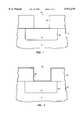
- FIGS. 1-5are schematic representations of process steps for forming an aluinum alloy contact in the contact window of a silicon device.
- a silicon substrate 11is shown with an impurity region 12.
- the substrate illustratedis p-type, and the impurity region 12 is n-type, typical of a source or drain for an n-channel silicon transistor.
- the figuresshow only a portion of the silicon device for illustration.
- the contact windowis shown at 13, and typically is formed during etchback of oxide 14.
- formation of the barrier layerbegins with the deposition of a layer 15 of Ti.
- the Ti layeris deposited using known techniques.
- the Ti layeris deposited using sputtering methods (PVD).
- PVDsputtering methods
- a collimated Ti film effective for the purposes of the inventioncan be deposited using a Varian M2i reactor, and sputtering a titanium target in pure argon at a temperature (pedestal) of 100-400° C., preferably, approximately 250° C., a pressure in the range 2-6 mTorr , and a power level in the range 3-10 kW, preferably approximately 6 kW.
- the thickness of layer 15is in the range 30-400 Angstroms, preferably approximately 50-150 Angstroms.
- a TiN layer 16is deposited on layer 15 as shown in FIG. 3.
- the TiN layeris shown substantially thicker than the titanium layer. It should be understood that the drawings are intended to be accurate qualitative representations of actual structures but are not drawn to scale.
- the TiN layeris deposited by CVD using precursors such as TDMAT or TDEAT according to known techniques.
- a CVD TiN layer suitable for the purposes of the inventioncan be produced in a CVD reactor at a temperature in the range 400-460° C. (pedestal), using TDMAT at a flow rate of 225 sccm in a carrier gas of He at 275 sccm.
- the CVD TiN layeris immediately followed by a layer of TiN deposited by sputtering (PVD-TiN) layer 17 as shown in FIG. 4.
- PVD-TiNTiN deposited by sputtering
- the PVD-TiNis deposited by sputtering from a Ti target in a mixture of argon/nitrogen with a ratio in the range 2:1 to 5:1.
- the deposition temperatureis in the range 100-400° C., preferably 225-275° C.
- the pressureis in the range 2-6 mTorr
- the power levelis in the range 18-24 kW, preferably approximately 20 kW.
- the PVD filmmay be deposited using collimated or ion assisted deposition techniques as is known in the art.
- the thickness of the PVD-TiN filmwill depend on the aspect ratio and dimensions of window 13 and the amount of coverage necessary to blanket the previously deposited CVD-TiN layer 16.
- the thickness of layer 17will be in the range 100-400 Angstroms, and preferably 200-300 Angstroms.
- layer 17is deposited at relatively low temperatures, preferably below 400° C.
- all depositionsi.e. layers 15-17 are carried out in the same apparatus, e.g. a cluster tool where layers 15-17 are deposited sequentially.
- a cluster toolwhere layers 15-17 are deposited sequentially.
- layers 15 and 16may be deposited in one tool and layer 17 in another, etc.
- the CVD-TiN layer 16is treated by a plasma to at least partially reorient the crystal structure of the film prior to deposition of the PVD-TiN film.
- a suitable plasma treatmentis 30 sec. at 1.3 mTorr, and 400-460° C., in an atmosphere of nitrogen and hydrogen.
- the Al-alloy contact layer 21is deposited in the window as shown in FIG. 5.
- the contact layeris 4000-15000 Angstroms thick, so as to essentially plug the opening 13 (shown as a window but as indicated earlier may be a via), as well as provide runners and interconnects as required.
- the Al layeris typically Al-Si with 0.5 to 2.0 wt % Si. Other alloys may be used such as Al with 0.5-2.0 wt % Cu, or ternary alloys of Al-Si-Cu. Ge or Sc may also be added for improved reliability.
- the Al metallizationis sputtered from an alloy target using known techniques.
- CVD Al deposition techniquecan be used, or one or more CVD Al layers can be alternated with one or more PVD Al layers with alloying elements for improved reliability. It is convenient, and effective from a cost standpoint, to deposit the Al layer 21 in the same apparatus used to deposit layers 15-17.
- Improved contact resistancecan be obtained in many cases by annealing the Ti-TiN layers prior to deposition of aluminum to form a silicide between the Ti layer and the silicon substrate or first level metal.
- the morphology of the Al-alloy filmtends to replicate that of the surface on which it deposits. Consequently, the Al-alloy layer 21 will replicate the texture of layer 16. Since the microstrcture and texture of the CVD-TiN layer without the PVD-TiN over-layer is highly irregular from region to region in the opening 13, the Al microstructure and texture on CVD-TiN alone will also be irregular. If, however, the Al-alloy layer 21 is deposited on the CVD-TiN/PVD-TiN stack, then the Al-alloy texture will preferentially adjust to a ⁇ 111> texture. In such a Ti/CVD-TiN/PVD-TiN composite structure, good step coverage is ensured by the CVD-TiN layer 16, and uniform crystal structure and texture is ensured by the PVD-TiN layer 17.
- barrier layers produced by the process just describedcan be further enhanced by forming an additional barrier layer between the composite CVD/PVD structure.
- This layercomprises titanium oxynitride.
- the layer thicknessshould be in the range 50-200 Angstroms.
- the oxynitride layercan be produced easily by bleeding oxygen into the reaction chamber during plasma passivation of the CVD TiN layer.
- CVDchemical vapor deposition
- PVDphysical vapor deposition
- siliconas mentioned above the invention may be applied to window plugs or interlevel plugs in silicon integrated circuits.
- siliconas used herein and in the appended claims is intended to cover single crystal silicon (substrate) or polysilicon (metallization).
Landscapes
- Chemical & Material Sciences (AREA)
- Engineering & Computer Science (AREA)
- Physics & Mathematics (AREA)
- Organic Chemistry (AREA)
- Metallurgy (AREA)
- Mechanical Engineering (AREA)
- Materials Engineering (AREA)
- Chemical Kinetics & Catalysis (AREA)
- Computer Hardware Design (AREA)
- Power Engineering (AREA)
- Microelectronics & Electronic Packaging (AREA)
- Manufacturing & Machinery (AREA)
- General Physics & Mathematics (AREA)
- Condensed Matter Physics & Semiconductors (AREA)
- Inorganic Chemistry (AREA)
- General Chemical & Material Sciences (AREA)
- Plasma & Fusion (AREA)
- Internal Circuitry In Semiconductor Integrated Circuit Devices (AREA)
- Electrodes Of Semiconductors (AREA)
- Chemical Vapour Deposition (AREA)
Abstract
Description
Claims (11)
Priority Applications (4)
| Application Number | Priority Date | Filing Date | Title |
|---|---|---|---|
| US08/941,556US5972179A (en) | 1997-09-30 | 1997-09-30 | Silicon IC contacts using composite TiN barrier layer |
| TW087114879ATW396566B (en) | 1997-09-30 | 1998-09-08 | Improved silicon IC contacts using composite TiN barrier layers |
| KR1019980040192AKR100298970B1 (en) | 1997-09-30 | 1998-09-28 | Silicon Integrated Circuit Manufacturing Method |
| JP27511798AJP3386385B2 (en) | 1997-09-30 | 1998-09-29 | Method for manufacturing silicon integrated circuit |
Applications Claiming Priority (1)
| Application Number | Priority Date | Filing Date | Title |
|---|---|---|---|
| US08/941,556US5972179A (en) | 1997-09-30 | 1997-09-30 | Silicon IC contacts using composite TiN barrier layer |
Publications (1)
| Publication Number | Publication Date |
|---|---|
| US5972179Atrue US5972179A (en) | 1999-10-26 |
Family
ID=25476685
Family Applications (1)
| Application Number | Title | Priority Date | Filing Date |
|---|---|---|---|
| US08/941,556Expired - LifetimeUS5972179A (en) | 1997-09-30 | 1997-09-30 | Silicon IC contacts using composite TiN barrier layer |
Country Status (4)
| Country | Link |
|---|---|
| US (1) | US5972179A (en) |
| JP (1) | JP3386385B2 (en) |
| KR (1) | KR100298970B1 (en) |
| TW (1) | TW396566B (en) |
Cited By (53)
| Publication number | Priority date | Publication date | Assignee | Title |
|---|---|---|---|---|
| US6086960A (en)* | 1995-03-28 | 2000-07-11 | Hyundai Electronics Industries Co., Ltd. | Method for improving the quality of a titanium nitride layer including carbon and oxygen |
| US6140223A (en)* | 1997-11-25 | 2000-10-31 | Samsung Electronics Co., Ltd. | Methods of forming contacts for integrated circuits using chemical vapor deposition and physical vapor deposition |
| US6177316B1 (en)* | 1999-10-05 | 2001-01-23 | Advanced Micro Devices, Inc. | Post barrier metal contact implantation to minimize out diffusion for NAND device |
| WO2001047011A1 (en)* | 1999-12-22 | 2001-06-28 | Infineon Technologies North America Corp. | A cvd/pvd/cvd/pvd fill process |
| US20010009807A1 (en)* | 1998-09-03 | 2001-07-26 | Micron Technology, Inc. | Small grain size, conformal aluminum interconnects and method for their formation |
| US20010010403A1 (en)* | 1998-09-10 | 2001-08-02 | Micron Technology, Inc. | Forming submicron integrated-circuit wiring from gold, silver, copper, and other metals |
| EP1122332A1 (en)* | 2000-02-03 | 2001-08-08 | Applied Materials, Inc. | Method and apparatus for deposition of low residual halogen content TiN film |
| US6358811B1 (en)* | 1998-11-05 | 2002-03-19 | Bae Yeon Kim | Method for forming a stoichiometric ferroelectric and/or dielectric thin film layer containing lead or bismuth on an electrode |
| US20020060363A1 (en)* | 1997-05-14 | 2002-05-23 | Applied Materials, Inc. | Reliability barrier integration for Cu application |
| WO2002012589A3 (en)* | 2000-08-09 | 2002-07-11 | Applied Materials Inc | Barrier layer structure for copper metallization and method of forming the structure |
| US6429120B1 (en)* | 2000-01-18 | 2002-08-06 | Micron Technology, Inc. | Methods and apparatus for making integrated-circuit wiring from copper, silver, gold, and other metals |
| US6436819B1 (en)* | 2000-02-01 | 2002-08-20 | Applied Materials, Inc. | Nitrogen treatment of a metal nitride/metal stack |
| US20020114880A1 (en)* | 2001-01-05 | 2002-08-22 | Carl Zeiss Semiconductor Manufacturing Technologies Ag | Coating of optical elements, in particular for use with ultraviolet light |
| US20020197863A1 (en)* | 2001-06-20 | 2002-12-26 | Mak Alfred W. | System and method to form a composite film stack utilizing sequential deposition techniques |
| US20030068894A1 (en)* | 2001-09-28 | 2003-04-10 | Infineon Technologies North America Corp. | Liner with poor step coverage to improve contact resistance in W contacts |
| US6559062B1 (en) | 2000-11-15 | 2003-05-06 | Agere Systems, Inc. | Method for avoiding notching in a semiconductor interconnect during a metal etching step |
| US20030091739A1 (en)* | 2001-11-14 | 2003-05-15 | Hitoshi Sakamoto | Barrier metal film production apparatus, barrier metal film production method, metal film production method, and metal film production apparatus |
| US6607976B2 (en)* | 2001-09-25 | 2003-08-19 | Applied Materials, Inc. | Copper interconnect barrier layer structure and formation method |
| US6610597B2 (en)* | 1999-08-17 | 2003-08-26 | Nec Corporation | Method of fabricating a semiconductor device |
| US6614099B2 (en) | 1998-08-04 | 2003-09-02 | Micron Technology, Inc. | Copper metallurgy in integrated circuits |
| US6656831B1 (en)* | 2000-01-26 | 2003-12-02 | Applied Materials, Inc. | Plasma-enhanced chemical vapor deposition of a metal nitride layer |
| US6699530B2 (en)* | 1995-07-06 | 2004-03-02 | Applied Materials, Inc. | Method for constructing a film on a semiconductor wafer |
| US6743716B2 (en) | 2000-01-18 | 2004-06-01 | Micron Technology, Inc. | Structures and methods to enhance copper metallization |
| US6747445B2 (en) | 2001-10-31 | 2004-06-08 | Agere Systems Inc. | Stress migration test structure and method therefor |
| US6767832B1 (en)* | 2001-04-27 | 2004-07-27 | Lsi Logic Corporation | In situ liner barrier |
| US6777328B2 (en)* | 2002-01-31 | 2004-08-17 | Oki Electric Industry Co., Ltd. | Method of forming multilayered conductive layers for semiconductor device |
| US6780752B1 (en)* | 2000-07-22 | 2004-08-24 | Hynix Semiconductor Inc. | Metal thin film of semiconductor device and method for forming same |
| US6790776B2 (en)* | 1999-08-16 | 2004-09-14 | Applied Materials, Inc. | Barrier layer for electroplating processes |
| US20040203230A1 (en)* | 2002-01-31 | 2004-10-14 | Tetsuo Usami | Semiconductor device having multilayered conductive layers |
| US20040219783A1 (en)* | 2001-07-09 | 2004-11-04 | Micron Technology, Inc. | Copper dual damascene interconnect technology |
| US6821571B2 (en)* | 1999-06-18 | 2004-11-23 | Applied Materials Inc. | Plasma treatment to enhance adhesion and to minimize oxidation of carbon-containing layers |
| US20040253807A1 (en)* | 2003-06-13 | 2004-12-16 | Taiwan Semiconductor Manufacturing Co., Ltd. | Barrier layer stack to prevent Ti diffusion |
| KR100475117B1 (en)* | 2002-11-19 | 2005-03-11 | 삼성전자주식회사 | Method for forming metal wiring layer of semiconductor device |
| US20050158990A1 (en)* | 2004-01-14 | 2005-07-21 | Park Jae-Hwa | Methods of forming metal wiring layers for semiconductor devices |
| US6972254B1 (en)* | 2001-06-01 | 2005-12-06 | Advanced Micro Devices, Inc. | Manufacturing a conformal atomic liner layer in an integrated circuit interconnect |
| US6995470B2 (en) | 2000-05-31 | 2006-02-07 | Micron Technology, Inc. | Multilevel copper interconnects with low-k dielectrics and air gaps |
| US7067421B2 (en) | 2000-05-31 | 2006-06-27 | Micron Technology, Inc. | Multilevel copper interconnect with double passivation |
| US20060148242A1 (en)* | 2004-12-31 | 2006-07-06 | Dongbuanam Semiconductor Inc. | Metallization method of semiconductor device |
| US7105914B2 (en) | 2000-01-18 | 2006-09-12 | Micron Technology, Inc. | Integrated circuit and seed layers |
| US7211512B1 (en) | 2000-01-18 | 2007-05-01 | Micron Technology, Inc. | Selective electroless-plated copper metallization |
| US7220665B2 (en) | 2003-08-05 | 2007-05-22 | Micron Technology, Inc. | H2 plasma treatment |
| US7253521B2 (en) | 2000-01-18 | 2007-08-07 | Micron Technology, Inc. | Methods for making integrated-circuit wiring from copper, silver, gold, and other metals |
| US20070272655A1 (en)* | 2001-11-14 | 2007-11-29 | Hitoshi Sakamoto | Barrier metal film production method |
| US20080054326A1 (en)* | 2006-09-06 | 2008-03-06 | International Business Machines Corporation | Low resistance contact structure and fabrication thereof |
| US20080070405A1 (en)* | 2002-05-30 | 2008-03-20 | Park Jae-Hwa | Methods of forming metal wiring layers for semiconductor devices |
| US20080138971A1 (en)* | 2004-06-14 | 2008-06-12 | Semiconductor Energy Laboratory Co., Ltd. | Manufacturing method of semiconductor device |
| US20100190353A1 (en)* | 2003-02-04 | 2010-07-29 | Tegal Corporation | Nanolayer deposition process |
| US20120202353A1 (en)* | 2001-09-10 | 2012-08-09 | Asm International N.V. | Nanolayer deposition using plasma treatment |
| US20130299901A1 (en)* | 2011-09-29 | 2013-11-14 | Force Mos Technology Co., Ltd. | Trench mosfet structures using three masks process |
| US9121098B2 (en) | 2003-02-04 | 2015-09-01 | Asm International N.V. | NanoLayer Deposition process for composite films |
| WO2015128399A3 (en)* | 2014-02-27 | 2015-10-22 | Commissariat à l'énergie atomique et aux énergies alternatives | Process for producing a structure by assembling at least two elements by direct adhesive bonding |
| DE102016104087A1 (en) | 2015-03-12 | 2016-09-15 | Kennametal Inc. | PVD coated cutting tools and method of making the same |
| US10542621B2 (en) | 2016-12-30 | 2020-01-21 | Samsung Display Co., Ltd. | Conductive pattern and display device having the same |
Families Citing this family (3)
| Publication number | Priority date | Publication date | Assignee | Title |
|---|---|---|---|---|
| KR100543458B1 (en)* | 2003-06-03 | 2006-01-20 | 삼성전자주식회사 | Method for forming conductive structure of semiconductor device |
| JP5670085B2 (en)* | 2010-04-05 | 2015-02-18 | 株式会社アルバック | Manufacturing method of semiconductor device |
| CN102263031A (en)* | 2010-05-26 | 2011-11-30 | 上海宏力半导体制造有限公司 | Method for manufacturing trench vertical metal oxide semiconductor (VMOS) transistor |
Citations (6)
| Publication number | Priority date | Publication date | Assignee | Title |
|---|---|---|---|---|
| US5232871A (en)* | 1990-12-27 | 1993-08-03 | Intel Corporation | Method for forming a titanium nitride barrier layer |
| US5378660A (en)* | 1993-02-12 | 1995-01-03 | Applied Materials, Inc. | Barrier layers and aluminum contacts |
| US5420072A (en)* | 1994-02-04 | 1995-05-30 | Motorola, Inc. | Method for forming a conductive interconnect in an integrated circuit |
| US5712193A (en)* | 1994-12-30 | 1998-01-27 | Lucent Technologies, Inc. | Method of treating metal nitride films to reduce silicon migration therein |
| US5776831A (en)* | 1995-12-27 | 1998-07-07 | Lsi Logic Corporation | Method of forming a high electromigration resistant metallization system |
| US5780356A (en)* | 1995-12-15 | 1998-07-14 | Hyundai Electronics Industires Co., Ltd. | Method for forming metal wire of semiconductor device |
- 1997
- 1997-09-30USUS08/941,556patent/US5972179A/ennot_activeExpired - Lifetime
- 1998
- 1998-09-08TWTW087114879Apatent/TW396566B/ennot_activeIP Right Cessation
- 1998-09-28KRKR1019980040192Apatent/KR100298970B1/ennot_activeExpired - Fee Related
- 1998-09-29JPJP27511798Apatent/JP3386385B2/ennot_activeExpired - Fee Related
Patent Citations (6)
| Publication number | Priority date | Publication date | Assignee | Title |
|---|---|---|---|---|
| US5232871A (en)* | 1990-12-27 | 1993-08-03 | Intel Corporation | Method for forming a titanium nitride barrier layer |
| US5378660A (en)* | 1993-02-12 | 1995-01-03 | Applied Materials, Inc. | Barrier layers and aluminum contacts |
| US5420072A (en)* | 1994-02-04 | 1995-05-30 | Motorola, Inc. | Method for forming a conductive interconnect in an integrated circuit |
| US5712193A (en)* | 1994-12-30 | 1998-01-27 | Lucent Technologies, Inc. | Method of treating metal nitride films to reduce silicon migration therein |
| US5780356A (en)* | 1995-12-15 | 1998-07-14 | Hyundai Electronics Industires Co., Ltd. | Method for forming metal wire of semiconductor device |
| US5776831A (en)* | 1995-12-27 | 1998-07-07 | Lsi Logic Corporation | Method of forming a high electromigration resistant metallization system |
Cited By (114)
| Publication number | Priority date | Publication date | Assignee | Title |
|---|---|---|---|---|
| US6086960A (en)* | 1995-03-28 | 2000-07-11 | Hyundai Electronics Industries Co., Ltd. | Method for improving the quality of a titanium nitride layer including carbon and oxygen |
| US20040099215A1 (en)* | 1995-07-06 | 2004-05-27 | Applied Materials, Inc. | Chamber for constructing a film on a semiconductor wafer |
| US6699530B2 (en)* | 1995-07-06 | 2004-03-02 | Applied Materials, Inc. | Method for constructing a film on a semiconductor wafer |
| US7026238B2 (en) | 1997-05-14 | 2006-04-11 | Applied Materials, Inc. | Reliability barrier integration for Cu application |
| US20070151861A1 (en)* | 1997-05-14 | 2007-07-05 | Ming Xi | Reliability barrier integration for cu application |
| US20030017695A1 (en)* | 1997-05-14 | 2003-01-23 | Applied Materials, Inc. | Reliability barrier integration for Cu application |
| US20020060363A1 (en)* | 1997-05-14 | 2002-05-23 | Applied Materials, Inc. | Reliability barrier integration for Cu application |
| US20030013297A1 (en)* | 1997-05-14 | 2003-01-16 | Applied Materials, Inc. | Reliability barrier integration for Cu application |
| US20040209460A1 (en)* | 1997-05-14 | 2004-10-21 | Ming Xi | Reliability barrier integration for Cu application |
| US6140223A (en)* | 1997-11-25 | 2000-10-31 | Samsung Electronics Co., Ltd. | Methods of forming contacts for integrated circuits using chemical vapor deposition and physical vapor deposition |
| US6614099B2 (en) | 1998-08-04 | 2003-09-02 | Micron Technology, Inc. | Copper metallurgy in integrated circuits |
| US6774487B2 (en)* | 1998-09-03 | 2004-08-10 | Micron Technology, Inc. | Small grain size, conformal aluminum interconnects and method for their formation |
| US7276795B2 (en) | 1998-09-03 | 2007-10-02 | Micron Technology, Inc. | Small grain size, conformal aluminum interconnects and method for their formation |
| US7217661B2 (en) | 1998-09-03 | 2007-05-15 | Micron Technology, Inc. | Small grain size, conformal aluminum interconnects and method for their formation |
| US20010009807A1 (en)* | 1998-09-03 | 2001-07-26 | Micron Technology, Inc. | Small grain size, conformal aluminum interconnects and method for their formation |
| US7560816B2 (en)* | 1998-09-03 | 2009-07-14 | Micron Technology, Inc. | Small grain size, conformal aluminum interconnects and method for their formation |
| US20060194434A1 (en)* | 1998-09-03 | 2006-08-31 | Micron Technology, Inc. | Small grain size, conformal aluminum interconnects and method for their formation |
| US20060014386A1 (en)* | 1998-09-03 | 2006-01-19 | Micron Technology, Inc. | Small grain size, conformal aluminum interconnects and method for their formation |
| US6946393B2 (en) | 1998-09-03 | 2005-09-20 | Micron Technology, Inc. | Small grain size, conformal aluminum interconnects and method for their formation |
| US7737024B2 (en) | 1998-09-03 | 2010-06-15 | Micron Technology, Inc. | Small grain size, conformal aluminum interconnects and method for their formation |
| US20050006774A1 (en)* | 1998-09-03 | 2005-01-13 | Micron Technology, Inc. | Small grain size, conformal aluminum interconnects and method for their formation |
| US6849927B2 (en) | 1998-09-10 | 2005-02-01 | Micron Technology, Inc. | Forming submicron integrated-circuit wiring from gold, silver, copper, and other metals |
| US20010010403A1 (en)* | 1998-09-10 | 2001-08-02 | Micron Technology, Inc. | Forming submicron integrated-circuit wiring from gold, silver, copper, and other metals |
| US6358811B1 (en)* | 1998-11-05 | 2002-03-19 | Bae Yeon Kim | Method for forming a stoichiometric ferroelectric and/or dielectric thin film layer containing lead or bismuth on an electrode |
| US7144606B2 (en) | 1999-06-18 | 2006-12-05 | Applied Materials, Inc. | Plasma treatment to enhance adhesion and to minimize oxidation of carbon-containing layers |
| US6821571B2 (en)* | 1999-06-18 | 2004-11-23 | Applied Materials Inc. | Plasma treatment to enhance adhesion and to minimize oxidation of carbon-containing layers |
| US20050031784A1 (en)* | 1999-08-16 | 2005-02-10 | Peijun Ding | Barrier layer for electroplating processes |
| US6790776B2 (en)* | 1999-08-16 | 2004-09-14 | Applied Materials, Inc. | Barrier layer for electroplating processes |
| US6610597B2 (en)* | 1999-08-17 | 2003-08-26 | Nec Corporation | Method of fabricating a semiconductor device |
| US6177316B1 (en)* | 1999-10-05 | 2001-01-23 | Advanced Micro Devices, Inc. | Post barrier metal contact implantation to minimize out diffusion for NAND device |
| WO2001047011A1 (en)* | 1999-12-22 | 2001-06-28 | Infineon Technologies North America Corp. | A cvd/pvd/cvd/pvd fill process |
| US7402516B2 (en) | 2000-01-18 | 2008-07-22 | Micron Technology, Inc. | Method for making integrated circuits |
| US7262130B1 (en) | 2000-01-18 | 2007-08-28 | Micron Technology, Inc. | Methods for making integrated-circuit wiring from copper, silver, gold, and other metals |
| US6756298B2 (en) | 2000-01-18 | 2004-06-29 | Micron Technology, Inc. | Methods and apparatus for making integrated-circuit wiring from copper, silver, gold, and other metals |
| US8779596B2 (en) | 2000-01-18 | 2014-07-15 | Micron Technology, Inc. | Structures and methods to enhance copper metallization |
| US7105914B2 (en) | 2000-01-18 | 2006-09-12 | Micron Technology, Inc. | Integrated circuit and seed layers |
| US7745934B2 (en) | 2000-01-18 | 2010-06-29 | Micron Technology, Inc. | Integrated circuit and seed layers |
| US7211512B1 (en) | 2000-01-18 | 2007-05-01 | Micron Technology, Inc. | Selective electroless-plated copper metallization |
| US6743716B2 (en) | 2000-01-18 | 2004-06-01 | Micron Technology, Inc. | Structures and methods to enhance copper metallization |
| US7670469B2 (en) | 2000-01-18 | 2010-03-02 | Micron Technology, Inc. | Methods and apparatus for making integrated-circuit wiring from copper, silver, gold, and other metals |
| US7535103B2 (en) | 2000-01-18 | 2009-05-19 | Micron Technology, Inc. | Structures and methods to enhance copper metallization |
| US6429120B1 (en)* | 2000-01-18 | 2002-08-06 | Micron Technology, Inc. | Methods and apparatus for making integrated-circuit wiring from copper, silver, gold, and other metals |
| US7253521B2 (en) | 2000-01-18 | 2007-08-07 | Micron Technology, Inc. | Methods for making integrated-circuit wiring from copper, silver, gold, and other metals |
| US7394157B2 (en) | 2000-01-18 | 2008-07-01 | Micron Technology, Inc. | Integrated circuit and seed layers |
| US7262505B2 (en) | 2000-01-18 | 2007-08-28 | Micron Technology, Inc. | Selective electroless-plated copper metallization |
| US7378737B2 (en) | 2000-01-18 | 2008-05-27 | Micron Technology, Inc. | Structures and methods to enhance copper metallization |
| US7368378B2 (en) | 2000-01-18 | 2008-05-06 | Micron Technology, Inc. | Methods for making integrated-circuit wiring from copper, silver, gold, and other metals |
| US7301190B2 (en) | 2000-01-18 | 2007-11-27 | Micron Technology, Inc. | Structures and methods to enhance copper metallization |
| US7285196B2 (en) | 2000-01-18 | 2007-10-23 | Micron Technology, Inc. | Methods and apparatus for making integrated-circuit wiring from copper, silver, gold, and other metals |
| US6656831B1 (en)* | 2000-01-26 | 2003-12-02 | Applied Materials, Inc. | Plasma-enhanced chemical vapor deposition of a metal nitride layer |
| US6436819B1 (en)* | 2000-02-01 | 2002-08-20 | Applied Materials, Inc. | Nitrogen treatment of a metal nitride/metal stack |
| US6436820B1 (en) | 2000-02-03 | 2002-08-20 | Applied Materials, Inc | Method for the CVD deposition of a low residual halogen content multi-layered titanium nitride film having a combined thickness greater than 1000 Å |
| EP1122332A1 (en)* | 2000-02-03 | 2001-08-08 | Applied Materials, Inc. | Method and apparatus for deposition of low residual halogen content TiN film |
| US7091611B2 (en) | 2000-05-31 | 2006-08-15 | Micron Technology, Inc. | Multilevel copper interconnects with low-k dielectrics and air gaps |
| US6995470B2 (en) | 2000-05-31 | 2006-02-07 | Micron Technology, Inc. | Multilevel copper interconnects with low-k dielectrics and air gaps |
| US7067421B2 (en) | 2000-05-31 | 2006-06-27 | Micron Technology, Inc. | Multilevel copper interconnect with double passivation |
| US20040262761A1 (en)* | 2000-07-22 | 2004-12-30 | Hynix Semiconductor Inc. | Metal thin film of semiconductor device and method for forming same |
| US6780752B1 (en)* | 2000-07-22 | 2004-08-24 | Hynix Semiconductor Inc. | Metal thin film of semiconductor device and method for forming same |
| US6562715B1 (en) | 2000-08-09 | 2003-05-13 | Applied Materials, Inc. | Barrier layer structure for copper metallization and method of forming the structure |
| WO2002012589A3 (en)* | 2000-08-09 | 2002-07-11 | Applied Materials Inc | Barrier layer structure for copper metallization and method of forming the structure |
| US6559062B1 (en) | 2000-11-15 | 2003-05-06 | Agere Systems, Inc. | Method for avoiding notching in a semiconductor interconnect during a metal etching step |
| US20020114880A1 (en)* | 2001-01-05 | 2002-08-22 | Carl Zeiss Semiconductor Manufacturing Technologies Ag | Coating of optical elements, in particular for use with ultraviolet light |
| US6767832B1 (en)* | 2001-04-27 | 2004-07-27 | Lsi Logic Corporation | In situ liner barrier |
| US6972254B1 (en)* | 2001-06-01 | 2005-12-06 | Advanced Micro Devices, Inc. | Manufacturing a conformal atomic liner layer in an integrated circuit interconnect |
| US20020197863A1 (en)* | 2001-06-20 | 2002-12-26 | Mak Alfred W. | System and method to form a composite film stack utilizing sequential deposition techniques |
| US6849545B2 (en) | 2001-06-20 | 2005-02-01 | Applied Materials, Inc. | System and method to form a composite film stack utilizing sequential deposition techniques |
| US20040219783A1 (en)* | 2001-07-09 | 2004-11-04 | Micron Technology, Inc. | Copper dual damascene interconnect technology |
| US20120202353A1 (en)* | 2001-09-10 | 2012-08-09 | Asm International N.V. | Nanolayer deposition using plasma treatment |
| US9708707B2 (en) | 2001-09-10 | 2017-07-18 | Asm International N.V. | Nanolayer deposition using bias power treatment |
| US6607976B2 (en)* | 2001-09-25 | 2003-08-19 | Applied Materials, Inc. | Copper interconnect barrier layer structure and formation method |
| US20030068894A1 (en)* | 2001-09-28 | 2003-04-10 | Infineon Technologies North America Corp. | Liner with poor step coverage to improve contact resistance in W contacts |
| US6734097B2 (en) | 2001-09-28 | 2004-05-11 | Infineon Technologies Ag | Liner with poor step coverage to improve contact resistance in W contacts |
| US6747445B2 (en) | 2001-10-31 | 2004-06-08 | Agere Systems Inc. | Stress migration test structure and method therefor |
| US7977243B2 (en) | 2001-11-14 | 2011-07-12 | Canon Anelva Corporation | Barrier metal film production apparatus, barrier metal film production method, metal film production method, and metal film production apparatus |
| EP1312696A3 (en)* | 2001-11-14 | 2004-01-07 | Mitsubishi Heavy Industries, Ltd. | Metal barrier film production apparatus, metal barrier film production method, metal film production method, and metal film production apparatus |
| US20070117363A1 (en)* | 2001-11-14 | 2007-05-24 | Hitoshi Sakamoto | Barrier metal film production apparatus, barrier metal film production method, metal film production method, and metal film production apparatus |
| US20070272655A1 (en)* | 2001-11-14 | 2007-11-29 | Hitoshi Sakamoto | Barrier metal film production method |
| US7659209B2 (en) | 2001-11-14 | 2010-02-09 | Canon Anelva Corporation | Barrier metal film production method |
| US20070087577A1 (en)* | 2001-11-14 | 2007-04-19 | Hitoshi Sakamoto | Barrier metal film production apparatus, barrier metal film production method, metal film production method, and metal film production apparatus |
| US20100047471A1 (en)* | 2001-11-14 | 2010-02-25 | Canon Anelva Corporation | Barrier metal film production apparatus, barrier metal film production method, metal film production method, and metal film production apparatus |
| US20030091739A1 (en)* | 2001-11-14 | 2003-05-15 | Hitoshi Sakamoto | Barrier metal film production apparatus, barrier metal film production method, metal film production method, and metal film production apparatus |
| US20060054593A1 (en)* | 2001-11-14 | 2006-03-16 | Hitoshi Sakamoto | Barrier metal film production apparatus, barrier metal film production method, metal film production method, and metal film production apparatus |
| US20100124825A1 (en)* | 2001-11-14 | 2010-05-20 | Canon Anelva Corporation | Barrier metal film production apparatus, barrier metal film production method, metal film production method, and metal film production apparatus |
| US20070141274A1 (en)* | 2001-11-14 | 2007-06-21 | Hitoshi Sakamoto | Barrier metal film production apparatus, barrier metal film production method, metal film production method, and metal film production apparatus |
| US20040203230A1 (en)* | 2002-01-31 | 2004-10-14 | Tetsuo Usami | Semiconductor device having multilayered conductive layers |
| US6777328B2 (en)* | 2002-01-31 | 2004-08-17 | Oki Electric Industry Co., Ltd. | Method of forming multilayered conductive layers for semiconductor device |
| US20080070405A1 (en)* | 2002-05-30 | 2008-03-20 | Park Jae-Hwa | Methods of forming metal wiring layers for semiconductor devices |
| KR100475117B1 (en)* | 2002-11-19 | 2005-03-11 | 삼성전자주식회사 | Method for forming metal wiring layer of semiconductor device |
| US9121098B2 (en) | 2003-02-04 | 2015-09-01 | Asm International N.V. | NanoLayer Deposition process for composite films |
| US9447496B2 (en) | 2003-02-04 | 2016-09-20 | Asm International N.V. | Nanolayer deposition process |
| US8940374B2 (en) | 2003-02-04 | 2015-01-27 | Asm International N.V. | Nanolayer deposition process |
| US8658259B2 (en) | 2003-02-04 | 2014-02-25 | Asm International N.V. | Nanolayer deposition process |
| US20100190353A1 (en)* | 2003-02-04 | 2010-07-29 | Tegal Corporation | Nanolayer deposition process |
| US7470992B2 (en)* | 2003-06-13 | 2008-12-30 | Taiwan Semiconductor Manufacturing Co., Ltd. | Barrier layer stack to prevent Ti diffusion |
| US7064056B2 (en)* | 2003-06-13 | 2006-06-20 | Taiwan Semiconductor Manufacturing Co., Ltd. | Barrier layer stack to prevent Ti diffusion |
| US20060261478A1 (en)* | 2003-06-13 | 2006-11-23 | Taiwan Semiconductor Manufacturing Co., Ltd. | Barrier layer stack to prevent ti diffusion |
| US20040253807A1 (en)* | 2003-06-13 | 2004-12-16 | Taiwan Semiconductor Manufacturing Co., Ltd. | Barrier layer stack to prevent Ti diffusion |
| US7220665B2 (en) | 2003-08-05 | 2007-05-22 | Micron Technology, Inc. | H2 plasma treatment |
| US7504674B2 (en) | 2003-08-05 | 2009-03-17 | Micron Technology, Inc. | Electronic apparatus having a core conductive structure within an insulating layer |
| US20050158990A1 (en)* | 2004-01-14 | 2005-07-21 | Park Jae-Hwa | Methods of forming metal wiring layers for semiconductor devices |
| US8258030B2 (en)* | 2004-06-14 | 2012-09-04 | Semiconductor Energy Laboratory Co., Ltd. | Manufacturing method of semiconductor device |
| US20080138971A1 (en)* | 2004-06-14 | 2008-06-12 | Semiconductor Energy Laboratory Co., Ltd. | Manufacturing method of semiconductor device |
| US20060148242A1 (en)* | 2004-12-31 | 2006-07-06 | Dongbuanam Semiconductor Inc. | Metallization method of semiconductor device |
| US7344974B2 (en)* | 2004-12-31 | 2008-03-18 | Dongbu Electronics Co., Ltd. | Metallization method of semiconductor device |
| US20080054326A1 (en)* | 2006-09-06 | 2008-03-06 | International Business Machines Corporation | Low resistance contact structure and fabrication thereof |
| US7407875B2 (en)* | 2006-09-06 | 2008-08-05 | International Business Machines Corporation | Low resistance contact structure and fabrication thereof |
| US20130299901A1 (en)* | 2011-09-29 | 2013-11-14 | Force Mos Technology Co., Ltd. | Trench mosfet structures using three masks process |
| WO2015128399A3 (en)* | 2014-02-27 | 2015-10-22 | Commissariat à l'énergie atomique et aux énergies alternatives | Process for producing a structure by assembling at least two elements by direct adhesive bonding |
| US20170025377A1 (en)* | 2014-02-27 | 2017-01-26 | Commissariat à l'énergie atomique et aux énergies alternatives | Process for producing a structure by assembling at least two elements by direct adhesive bonding |
| US9922953B2 (en)* | 2014-02-27 | 2018-03-20 | Commissariat A L'energie Atomique Et Aux Energies Alternatives | Process for producing a structure by assembling at least two elements by direct adhesive bonding |
| DE102016104087A1 (en) | 2015-03-12 | 2016-09-15 | Kennametal Inc. | PVD coated cutting tools and method of making the same |
| US9650713B2 (en) | 2015-03-12 | 2017-05-16 | Kennamtetal Inc. | PVD-coated cutting tools and method for making the same |
| US10253410B2 (en) | 2015-03-12 | 2019-04-09 | Kennametal Inc. | PVD-coated cutting tools and method for making the same |
| US10542621B2 (en) | 2016-12-30 | 2020-01-21 | Samsung Display Co., Ltd. | Conductive pattern and display device having the same |
Also Published As
| Publication number | Publication date |
|---|---|
| KR19990030184A (en) | 1999-04-26 |
| TW396566B (en) | 2000-07-01 |
| KR100298970B1 (en) | 2001-10-19 |
| JP3386385B2 (en) | 2003-03-17 |
| JPH11163141A (en) | 1999-06-18 |
Similar Documents
| Publication | Publication Date | Title |
|---|---|---|
| US5972179A (en) | Silicon IC contacts using composite TiN barrier layer | |
| US6607976B2 (en) | Copper interconnect barrier layer structure and formation method | |
| US5834372A (en) | Pretreatment of semiconductor substrate | |
| US6537910B1 (en) | Forming metal silicide resistant to subsequent thermal processing | |
| US7838441B2 (en) | Deposition and densification process for titanium nitride barrier layers | |
| US8053365B2 (en) | Methods for forming all tungsten contacts and lines | |
| US5378660A (en) | Barrier layers and aluminum contacts | |
| JP3094004B2 (en) | Method for CVD deposition of tungsten layer on semiconductor wafer | |
| US6518167B1 (en) | Method of forming a metal or metal nitride interface layer between silicon nitride and copper | |
| US6566246B1 (en) | Deposition of conformal copper seed layers by control of barrier layer morphology | |
| US5633200A (en) | Process for manufacturing a large grain tungsten nitride film and process for manufacturing a lightly nitrided titanium salicide diffusion barrier with a large grain tungsten nitride cover layer | |
| US7799674B2 (en) | Ruthenium alloy film for copper interconnects | |
| US6554914B1 (en) | Passivation of copper in dual damascene metalization | |
| US6534404B1 (en) | Method of depositing diffusion barrier for copper interconnect in integrated circuit | |
| US6066358A (en) | Blanket-selective chemical vapor deposition using an ultra-thin nucleation layer | |
| JPH11172438A (en) | Method for forming metal nitride film by chemical vapor deposition and method for forming metal contact of semiconductor device using the same | |
| US6054382A (en) | Method of improving texture of metal films in semiconductor integrated circuits | |
| US5582881A (en) | Process for deposition of a Ti/TiN cap layer on aluminum metallization and apparatus | |
| US6436820B1 (en) | Method for the CVD deposition of a low residual halogen content multi-layered titanium nitride film having a combined thickness greater than 1000 Å | |
| US6120842A (en) | TiN+Al films and processes | |
| JPH09186102A (en) | Method for manufacturing semiconductor device | |
| US20020025671A1 (en) | Method of manufacturing a metal line in a semiconductor device | |
| EP0840363A1 (en) | Method for fabricating a conductive diffusion barrier layer by PECVD | |
| JPH09260306A (en) | Thin film formation method | |
| EP0839927A2 (en) | Method of forming films comprising TiN and Al |
Legal Events
| Date | Code | Title | Description |
|---|---|---|---|
| AS | Assignment | Owner name:LUCENT TECHNOLOGIES INC., NEW JERSEY Free format text:ASSIGNMENT OF ASSIGNORS INTEREST;ASSIGNORS:CHITTIPEDDI, SAILESH;MERCHANT, SAILESH MANSINH;REEL/FRAME:009091/0169;SIGNING DATES FROM 19970313 TO 19970318 | |
| STCF | Information on status: patent grant | Free format text:PATENTED CASE | |
| FEPP | Fee payment procedure | Free format text:PAYOR NUMBER ASSIGNED (ORIGINAL EVENT CODE: ASPN); ENTITY STATUS OF PATENT OWNER: LARGE ENTITY | |
| FEPP | Fee payment procedure | Free format text:PAYOR NUMBER ASSIGNED (ORIGINAL EVENT CODE: ASPN); ENTITY STATUS OF PATENT OWNER: LARGE ENTITY Free format text:PAYER NUMBER DE-ASSIGNED (ORIGINAL EVENT CODE: RMPN); ENTITY STATUS OF PATENT OWNER: LARGE ENTITY | |
| FPAY | Fee payment | Year of fee payment:4 | |
| FPAY | Fee payment | Year of fee payment:8 | |
| FPAY | Fee payment | Year of fee payment:12 | |
| AS | Assignment | Owner name:AVAGO TECHNOLOGIES GENERAL IP (SINGAPORE) PTE. LTD Free format text:ASSIGNMENT OF ASSIGNORS INTEREST;ASSIGNOR:AGERE SYSTEMS LLC;REEL/FRAME:035365/0634 Effective date:20140804 | |
| AS | Assignment | Owner name:BANK OF AMERICA, N.A., AS COLLATERAL AGENT, NORTH CAROLINA Free format text:PATENT SECURITY AGREEMENT;ASSIGNOR:AVAGO TECHNOLOGIES GENERAL IP (SINGAPORE) PTE. LTD.;REEL/FRAME:037808/0001 Effective date:20160201 Owner name:BANK OF AMERICA, N.A., AS COLLATERAL AGENT, NORTH Free format text:PATENT SECURITY AGREEMENT;ASSIGNOR:AVAGO TECHNOLOGIES GENERAL IP (SINGAPORE) PTE. LTD.;REEL/FRAME:037808/0001 Effective date:20160201 | |
| AS | Assignment | Owner name:AVAGO TECHNOLOGIES GENERAL IP (SINGAPORE) PTE. LTD., SINGAPORE Free format text:TERMINATION AND RELEASE OF SECURITY INTEREST IN PATENTS;ASSIGNOR:BANK OF AMERICA, N.A., AS COLLATERAL AGENT;REEL/FRAME:041710/0001 Effective date:20170119 Owner name:AVAGO TECHNOLOGIES GENERAL IP (SINGAPORE) PTE. LTD Free format text:TERMINATION AND RELEASE OF SECURITY INTEREST IN PATENTS;ASSIGNOR:BANK OF AMERICA, N.A., AS COLLATERAL AGENT;REEL/FRAME:041710/0001 Effective date:20170119 | |
| AS | Assignment | Owner name:BELL SEMICONDUCTOR, LLC, ILLINOIS Free format text:ASSIGNMENT OF ASSIGNORS INTEREST;ASSIGNORS:AVAGO TECHNOLOGIES GENERAL IP (SINGAPORE) PTE. LTD.;BROADCOM CORPORATION;REEL/FRAME:044886/0001 Effective date:20171208 | |
| AS | Assignment | Owner name:CORTLAND CAPITAL MARKET SERVICES LLC, AS COLLATERA Free format text:SECURITY INTEREST;ASSIGNORS:HILCO PATENT ACQUISITION 56, LLC;BELL SEMICONDUCTOR, LLC;BELL NORTHERN RESEARCH, LLC;REEL/FRAME:045216/0020 Effective date:20180124 | |
| AS | Assignment | Owner name:BELL NORTHERN RESEARCH, LLC, ILLINOIS Free format text:SECURITY INTEREST;ASSIGNOR:CORTLAND CAPITAL MARKET SERVICES LLC;REEL/FRAME:060885/0001 Effective date:20220401 Owner name:BELL SEMICONDUCTOR, LLC, ILLINOIS Free format text:SECURITY INTEREST;ASSIGNOR:CORTLAND CAPITAL MARKET SERVICES LLC;REEL/FRAME:060885/0001 Effective date:20220401 Owner name:HILCO PATENT ACQUISITION 56, LLC, ILLINOIS Free format text:SECURITY INTEREST;ASSIGNOR:CORTLAND CAPITAL MARKET SERVICES LLC;REEL/FRAME:060885/0001 Effective date:20220401 |