US5969779A - Liquid crystal display having a repair line - Google Patents
Liquid crystal display having a repair lineDownload PDFInfo
- Publication number
- US5969779A US5969779AUS08/708,224US70822496AUS5969779AUS 5969779 AUS5969779 AUS 5969779AUS 70822496 AUS70822496 AUS 70822496AUS 5969779 AUS5969779 AUS 5969779A
- Authority
- US
- United States
- Prior art keywords
- repair
- lines
- line
- data
- data lines
- Prior art date
- Legal status (The legal status is an assumption and is not a legal conclusion. Google has not performed a legal analysis and makes no representation as to the accuracy of the status listed.)
- Expired - Lifetime
Links
Images


Classifications
- G—PHYSICS
- G02—OPTICS
- G02F—OPTICAL DEVICES OR ARRANGEMENTS FOR THE CONTROL OF LIGHT BY MODIFICATION OF THE OPTICAL PROPERTIES OF THE MEDIA OF THE ELEMENTS INVOLVED THEREIN; NON-LINEAR OPTICS; FREQUENCY-CHANGING OF LIGHT; OPTICAL LOGIC ELEMENTS; OPTICAL ANALOGUE/DIGITAL CONVERTERS
- G02F1/00—Devices or arrangements for the control of the intensity, colour, phase, polarisation or direction of light arriving from an independent light source, e.g. switching, gating or modulating; Non-linear optics
- G02F1/01—Devices or arrangements for the control of the intensity, colour, phase, polarisation or direction of light arriving from an independent light source, e.g. switching, gating or modulating; Non-linear optics for the control of the intensity, phase, polarisation or colour
- G02F1/13—Devices or arrangements for the control of the intensity, colour, phase, polarisation or direction of light arriving from an independent light source, e.g. switching, gating or modulating; Non-linear optics for the control of the intensity, phase, polarisation or colour based on liquid crystals, e.g. single liquid crystal display cells
- G02F1/133—Constructional arrangements; Operation of liquid crystal cells; Circuit arrangements
- G02F1/136—Liquid crystal cells structurally associated with a semi-conducting layer or substrate, e.g. cells forming part of an integrated circuit
- G02F1/1362—Active matrix addressed cells
- G02F1/136204—Arrangements to prevent high voltage or static electricity failures
- G—PHYSICS
- G02—OPTICS
- G02F—OPTICAL DEVICES OR ARRANGEMENTS FOR THE CONTROL OF LIGHT BY MODIFICATION OF THE OPTICAL PROPERTIES OF THE MEDIA OF THE ELEMENTS INVOLVED THEREIN; NON-LINEAR OPTICS; FREQUENCY-CHANGING OF LIGHT; OPTICAL LOGIC ELEMENTS; OPTICAL ANALOGUE/DIGITAL CONVERTERS
- G02F1/00—Devices or arrangements for the control of the intensity, colour, phase, polarisation or direction of light arriving from an independent light source, e.g. switching, gating or modulating; Non-linear optics
- G02F1/01—Devices or arrangements for the control of the intensity, colour, phase, polarisation or direction of light arriving from an independent light source, e.g. switching, gating or modulating; Non-linear optics for the control of the intensity, phase, polarisation or colour
- G02F1/13—Devices or arrangements for the control of the intensity, colour, phase, polarisation or direction of light arriving from an independent light source, e.g. switching, gating or modulating; Non-linear optics for the control of the intensity, phase, polarisation or colour based on liquid crystals, e.g. single liquid crystal display cells
- G02F1/133—Constructional arrangements; Operation of liquid crystal cells; Circuit arrangements
- G02F1/136—Liquid crystal cells structurally associated with a semi-conducting layer or substrate, e.g. cells forming part of an integrated circuit
- G02F1/1362—Active matrix addressed cells
- G02F1/136259—Repairing; Defects
Definitions
- the present inventionrelates in general to a liquid crystal display, and more particularly, to a liquid crystal display having a repair line.
- a thin film transistor TFT liquid crystal display LCDis a display which uses a TFT for a switching element and uses the electro-optical effect of a liquid crystal material to create an image.
- Such an LCDfor each pixel, includes a TFT and a pixel electrode, a gate line to provide a switching signal to the pixel, a TFT substrate in which a data line is formed to provide a picture signal, a color filter substrate in which a common electrode and color filter are formed, and a liquid crystal material intervened between them.
- Gate lines and data lines providing signal paths to a pixelare formed in the TFT substrate of an LCD, but are apt to be broken in the process of creating product. If such lines are broken, the LCD may not perform properly as a display.
- One conventional method of solving this problemis to use a repair line in place of a broken wire when the break occurs after forming an enclosed curve type repair line around a screen formed of pixels. This intersects with gate lines and data lines with a gate insulating layer between them.
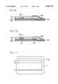
- FIG. 1is a plan view illustrating a conventional LCD wherein a repair line is formed as an enclosed curve around a screen
- FIG. 2is an equivalent circuit diagram of a general pixel
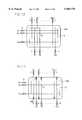
- FIG. 3is a plan view illustrating the layout of the lower substrate in FIG. 2.
- FIG. 4is a sectional view illustrating a section cut along A--A line in FIG. 3.
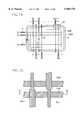
- FIG. 5is a diagram illustrating in greater detail portion 6 of FIG. 1, and FIG. 6 is a sectional view illustrating a section along the B--B line of FIG. 5.
- gate lines G 1 , G 2 , . . . G mare formed in parallel and data lines D 1 , D 2 , D 3 , D 4 , . . . D 2n-1 , D 2n intersecting perpendicular to them are formed.
- Input pads 1, 1', 2are formed on each row of data lines D 1 , D 2 , D 3 , D 4 , . . . D 2n-1 , D 2n and gate lines G 1 , G 2 , . . . , G m .
- the data linesmay be divided into several first data lines D 1 , D 3 , . . . D 2n-1 in which each input pad 1 is formed in the upper part of the LCD and second data lines D 2 , D 4 , . . . D 2n in which each input pad 1' is formed in the lower part of the LCD.
- Pixels 10are formed in the spaces at which the gate lines G 1 , G 2 , . . . , G m and data lines D 1 , D 2 , D 3 , D 4 , . . . D 2n-1 , D 2n meet.
- each pixel 10includes a switching element, generally TFT 20, a liquid crystal storage capacitor 13, and a holding capacitor 14.
- Liquid crystal storage capacitor 13is formed by a lower pixel electrode 12, an upper common electrode 11 and liquid crystal material between them.
- Such a pixel 10is connected to one data line and one gate line through TFT 20.
- FIGS. 3 and 4A lay-out of the upper portion of the pixel electrode and a section of TFT 20 corresponding to the upper part of a pixel having a structure as in FIG. 2 is illustrated in FIGS. 3 and 4.
- a gate line G and a gate electrode 22which are connected to it are formed.
- a gate oxide film 23is formed over each gate line G and gate electrode 22.
- a gate insulation layer 24covers oxide film 23, and substrate 21.
- a semiconductor layer 25Over the gate insulation layer 24, at the portion covering the gate electrode 22, is formed a semiconductor layer 25.
- the semiconductor layerwhich is typically formed of amorphous silicon, two divided contact layers 26 are formed, typically of n + amorphous silicon.
- a source electrode 27 of the TFTconnects to the data line D and covers one of the contact layers 26.
- a drain electrode 28 separated from the source electrode 27 and connected to the pixel electrode 12covers the other contact layer 26.
- the contact layersserve to improve the electric connection from the semiconductor layer 25 to the source and drain electrodes 27, 28.
- FIG. 1illustrates a repair line 100 formed in a enclosed curve around a screen 3 formed of pixels 10.
- Such a repair line 100intersects with each gate line G 1 , G 2 , . . . , G m around a input pad 2 and each data line D 1 , D 2 , D 3 , D 4 , . . . D 2n-1 , D 2n a first time around the input pad 1, 1' and a second time at the opposite end of the data line.
- Each data line D 1 , D 2 , D 3 , D 4 , . . . D 2n-1 , D 2nhas the same width throughout.
- data lines D 1 , D 2 , D 3 , D 4 , . . . D 2n-1 , D 2n and repair lineshave a same intersecting area respectively.
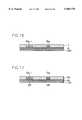
- FIGS. 5 and 6illustrates the intersecting of data lines D 2n-1 , D 2n and a repair line 100.
- a first data line D 2n-1 and a second data line D 2nhas a same intersecting area with a repair line 100.
- a gate insulation layer 24 formed on the repair line 100insulates repair line 100 from the data lines D 2n-1 , D 2n .
- a protective film 29is formed on the data lines D 2n-1 , D 2n . Accordingly, the intersecting area between the data lines D 2n-1 , D 2n and the repair line 100 acts as an undesired capacitor and parallel connected capacitors result.
- a switching signalis applied to each pixel 10 in turn through gate lines G 1 , G 2 , . . . , G m , a picture signal is applied to the corresponding pixel 10 through data lines D 1 , D 2 , D 3 , D 4 , . . . D 2n-1 , D 2n and provides an image in accordance with it.
- a data linesuch as D 3 is disconnected as illustrated in FIG. 1, the picture signal applied through the data line D 3 reaches the disconnected point but does not reach the next point. Thus, this picture signal cannot be applied to a pixel connected to the data line D 3 below the break or disconnect point illustrated with the symbol "//".
- the signalreaches the data line D 3 below the disconnected point.
- the area indicated with ⁇where the data line D 3 and the repair line 100 intersect, is short-circuited using a laser.
- a signal applied from a input pad 1 in a pixel connected to the data line D 3 below the disconnected pointafter passing through the upper of the disconnected intersecting area, moves along the left path of the data line D 3 through the repair line 100 connected with the data line D 3 (path P1) or along the right path (path P 2 ).
- path P1is longer than the path P 1 and intersects with many data lines, it can less efficiently transmit signals.
- the part from the break or disconnection position ⁇ to the path P 2is cut off, as indicated with an x. Therefore, it is possible to apply signals through the path P 1 of the repair line 100 into the data line D 3 below the disconnected point.
- a signal applied through the path P 1must pass through the intersecting areas a, a' between data lines D 1 , D 2 and the repair line 100.
- These areas a, a'act as capacitors and distort picture signals passing through the repair line 100.
- the number of intersecting areas and capacitors along the signal pathincrease and the overall electrostatic capacity grows. Because the length of the repair line 100 is also increased, the resistance increases. Consequently, distortion of the signals transferring through the repair line 100 undesirably occurs.
- the overall electrostatic capacityshould be reduced. Since the number of the wires cannot be reduced, the electrostatic capacity of the capacitors formed by the intersecting areas between the repair line 100 and data lines D 1 , D 2 , D 3 , D 4 , . . . D 2n-1 , D 2n should be reduced. Because the electrostatic capacity of these capacitors is proportional to the size of the intersecting area and is inversely proportional to the perpendicular length between the repair line 100 and data lines D 1 , D 2 , D 3 , D 4 , . . .
- D 2n-1 , D 2nin order to reduce the electrostatic capacity, the size of intersecting areas should be decreased, or the perpendicular length between the repair line 100 and data lines D 1 , D 2 , D 3 , D 4 , . . . D 2n-1 , D 2n should be increased.
- An object of the present inventionis to overcome problems with conventional repair lines and to efficiently perform the function of repairing broken data lines without adversely affecting quality.
- the present inventionreduces overall electrostatic capacity by effectively reducing capacitor surface area.
- each data lineis formed so that it directly intersects or overlaps a repair line that surrounds the LCD screen a single time at an end of the data line corresponding to a data line input pad.
- the other end of the data linedoes not intersect with the repair line, but instead uses a conductive layer that overlaps this other end of the data line at one end and the repair line at another end.
- this conductive layercan be fused in two places to perform a repair operation, but if a repair operation is not needed, since the data line does not directly intersect with the repair line, the overall electrostatic capacity is reduced.
- a plurality of repair lines that each surround the LCD screenare used. Groups of data lines are associated with one repair line and the widths of the data lines are narrowed if the data line intersects a repair line that it is not associated with. Accordingly, the width of the data lines that intersect an associated repair line is still wide enough to perform using operation if needed, but by reducing the width of data lines where they intersect non-associated repair lines, the overall electrostatic is reduced.
- FIG. 1is a plan view illustrating a conventional LCD wherein a repair line is formed as an enclosed curve around a screen.
- FIG. 2is an equivalent circuit diagram of a general pixel.
- FIG. 3is a plan view illustrating the layout of the lower substrate in FIG. 2.
- FIG. 4is a sectional view illustrating a section view taken along line A--A of FIG. 3.
- FIG. 5is a diagram illustrating in greater detail portion 6 of FIG. 1.
- FIG. 6is a sectional view illustrating a section taken along line B--B of FIG. 5.
- FIG. 7is a plan view illustrating an LCD according to the first preferred embodiment of the present invention.
- FIG. 8is a diagram illustrating in greater detail portion 7 of FIG. 7.
- FIGS. 9 and 10are sectional views illustrating different embodiments in a section taken along line C--C of FIG. 8.
- FIGS. 11 to 13are plan views illustrating a manufacturing method of an LCD according to the first preferred embodiment of the present invention.
- FIG. 14is a plan view illustrating an LCD according to the second preferred embodiment of the present invention.
- FIG. 15is a diagram illustrating in greater detail portion 8 of FIG. 14.
- FIGS. 16 and 17are sectional views illustrating different embodiments in a section taken along line D--D of FIG. 15.
- FIGS. 18 and 19are plan views illustrating the manufacturing method for an LCD according to the second preferred embodiment of the present invention.
- FIG. 20is a plan view of another embodiment of the invention which uses a plurality of repair lines.
- FIG. 7is a plan view illustrating an LCD according to the first preferred embodiment of the present invention
- FIG. 8is a diagram illustrating portion 7 of FIG. 7 in greater detail
- FIGS. 9 and 10are sectional views illustrating two embodiments of the present invention along a C--C section line in FIG. 8.
- An LCD according to this preferred embodiment of the present inventionis formed so that the direct intersecting between a repair line 100 and each data line D 1 , D 2 , D 3 , D 4 , . . . D 2n-1 , D 2n occurs only one time for each input pad 1, 1'.
- the opposite ends of each data line D 1 , D 2 , D 3 , D 4 , . . . D 2n-1 , D 2ndo not reach the repair line 100.
- each data line 1, 1'does not reach the repair line 100. Instead, the repair line 100 intersects with a conductive layer 300 with the protective film 29 in between which, in turn, intersects with the opposite end of a data line.
- the repair line 100is insulated from the data lines by a gate insulating layer 24.
- a protective film 29encapsulates the data lines.
- the intersecting between the conductive layer 300 and the repair line 100can advantageously include an intersecting semiconductor layer 25'.
- the end of data line D 2n opposite the input pad and the repair lineare connected using two series capacitors that are each fused together.
- the intersecting area semiconductor layer 25'is also formed for the intersecting of an adjacent data line having an input pad // on the opposite end as the input pads 1.
- the width of conductive layer 300is the same as that of the data line
- the thickness of the gate insulating layer 24is the same as that of the protective film 29 where the protective film is between conductive layer 300 and the repair line
- the electrostatic capacity C 0is generated by the result of the data line D 2n-1 intersecting with the repair line 100. Therefore, because the electrostatic capacity of each of the two capacitors shown in FIGS. 5 and 6 are C 0 respectively, the overall electrostatic capacity C 1 without their being connected when a conventional repair circuit is used becomes
- the electrostatic capacity generated by the conductive layer 300 intersecting with the repair line 100is Co/2 and the electrostatic capacity generated by the conductive layer 300 intersecting with the data line D 2n is C 0 . Therefore, the electrostatic capacity of these two capacitors without their being connected with each other, in series, is: ##EQU1##
- the electrostatic capacity generated by the conductive layer 300 intersecting with the data line D 2nis C 0
- the overall electrostatic capacity C 2is: ##EQU2##
- the preferred embodiment of the present inventionreduces the overall electrostatic capacity by 2/3 or more in comparison with a conventional LCD.
- the repair methodis as follows. As illustrated in FIG. 7, suppose that a data line D 3 is disconnected. The disconnect point is expressed by the symbol "//". In such a case, since a picture signal applied through the data line D 3 reaches the disconnected point but no further, the picture signal is not applied to a pixel 10 connected with the data line D 3 below the disconnected point.
- the intersecting area between the data line D 3 and the repair line 100 indicated with ⁇is short-circuited by laser. Also, because the opposite end of the data line is connected with the repair line 100 via conductive layer 300, the repair line 100 and the conductive layer 300 are short-circuited by laser and the conductive layer 300 and the opposite end of data line D 3 are short-circuited by laser. Finally, the point indicated with an x is cut so that the signal from the input pad 1 may reach the disconnected point only via path P 1 .
- FIGS. 3, 4 and 11explain how to make an LCD according to the preferred embodiment of the present invention.
- gate lines G 1 , G 2 , . . . , G mrespectively connected gate electrodes 22, and a repair line 100 are formed by laminating and photoengraving a metal as aluminum Al, aluminum alloy, chromium Cr and tantalum Ta on a transparent insulated substrate 21. So that the repair line 100 and the gate lines G 1 , G 2 , . . . , G m are not short-circuited, the gate lines G 1 , G 2 , . . . , G m do not have their whole length and input pads 2 in FIG. 7 of the gate lines G 1 , G 2 , . . . , G m are not formed (See FIG. 11).
- anode oxidation film 23As shown in FIG. 4 by anode oxidation to this structure, the ends of the gate lines G 1 , G 2 , . . . , G m that will be subsequently connected with the remainder of the respective gate lines G 1 , G 2 , . . . , G m and their input pads 2.
- a gate insulating layer 24is formed by laminating a material as silicon nitride SiN x and silicon oxidation SiO 2 throughout.
- the insulating layer 24is removed on the end of the gate lines G 1 , G 2 , . . . G m at the desired input pads locations.
- an amorphous siliconis laminated throughout.
- an n + amorphous siliconcan also be laminated over the amorphous silicon so that a good electric contact results between the subsequently formed source and drain electrodes 27, 28, and this semiconductor layer.
- a semiconductor layer 25 and contact layer 20 covering each gate electrode 22is formed by photoengraving the n + amorphous silicon layer and amorphous silicon.
- An intersecting area of semiconductor layer 25'may be left at an intersecting area for conductive layer 300 to assist with short-circuiting repair line 100 and conductive layer 300.
- data lines D 1 , D 2 , D 3 , D 4 , . . . D 2n-1 , D 2n , and data line input pads 1, 1', source and drain electrodes 27, 28, gate line input pads 2 and a part of the connected gate lineare formed.
- the end of the data lines D 1 , D 2 , D 3 , D 4 , . . . D 2n-1 , D 2nshould be formed so that their opposite ends do not reach the repair line 100.
- a protective film 29is formed by using a material as SiN x , and the protective film 29 on the drain electrode 28 is removed photoengraving (See FIG. 4).
- repair line 100 and the data line D 1 , D 2 , D 3 , D 4 , . . . D 2n-1 , D 2nare formed according to such a method, it is possible to avoid the distortion of the signal by reducing the overall electrostatic capacity.
- FIGS. 14 and 17explain another preferred embodiment of the present invention.
- This preferred embodimentdiffers from the first preferred embodiment by dividing data lines into several groups and has an exclusive repair line for each group.
- FIG. 14is a plan view illustrating an LCD according to the second preferred embodiment of the present invention
- FIG. 15is a diagram illustrating in greater detail portion 8 in FIG. 14
- FIGS. 16 and 17are sectional views illustrating two embodiments by a D--D line section in FIG. 15.
- repair lines 100, 200are formed in duplicate around the circumference of an LCD screen. Though illustrating the repair lines 100, 200 formed in duplicate in FIG. 14, the repair lines may be formed in triplicate, quadruplex or more.
- the first repair line 100is used as the exclusive repair line for first data lines D 1 , D 3 , . . . D 2n-1 and the second repair line 200 is used as the exclusive repair line for second data lines D 2 , D 4 , . . . , D 2n .
- the size of the intersecting area between each data line D 1 , D 2 , D 3 , D 4 , . . . D 2n-1 , D 2n and the associated repair linemaintains the minimum size needed to short-circuit elements if needed.
- each data line D 1 , D 2 , D 3 , D 4 , . . . D 2n-1 , D 2n , and the non-associated repair lineis smaller by adjusting the width of the first data lines so they are larger at an area where a short-circuit may be needed.
- the data line D 3is repaired using the repair lines 100, 200. Because the exclusive repair line for the first data lines D 1 , D 3 , . . . , D 2n-1 is the first repair line 100, the intersect area between the first data line D 3 and the repair line 100 indicated by ⁇ is short-circuited using a laser. If the point indicated with x is cut off, the signal from the input pad 1 may reach the disconnected point via a path P 1 of the first repair line 100.
- the signalmay flow via the second repair line 200 by short-circuiting the intersecting area between the second repair line 200 and the disconnected data line.
- the electrostatic capacity of the first repair line 100 or the second repair line 200is as follows.
- this preferred embodiment of the present inventionbrings about an effect that the overall electrostatic capacity is reduced 3/4 or more in comparison with a conventional LCD.
- the conventional electrostatic capacityis 3C 0 , the overall electrostatic capacity is reduced 2/3 in comparison with the conventional electrostatic capacity.
- FIGS. 3, 4, 18 and 19explain how to make a TFT for an LCD according to the second preferred embodiment of the present invention.
- gate lines G 1 , G 2 , . . . , G m , gate electrodes 22 respectively connected with them and repair lines 100, 200are formed by laminating and photoengraving a metal as aluminum Al, aluminum alloy, chromium Cr and tantalum Ta on transparent insulated substrate 21. So that the repair lines 100, 200 and the gate lines G 1 , G 2 , . . . G m are not short-circuited, the gate lines G 1 , G 2 , . . . G m do not have their whole length and input pads 2 formed. It is desirable to form an anode oxidation film 23 as shown in FIG.
- a gate insulating layer 24is formed by laminating a material as silicon nitride SiN x and silicon oxidation SiO 2 throughout.
- the insulating layer 24is removed at the desired input pad locations G 1 , G 2 , . . . , G m , with which the end of the gate lines G 1 , G 2 , . . . , G m and the input pad (the drawing code 2 in FIG. 7).
- an amorphous siliconis laminated throughout.
- an, n + amorphous siliconcan also be laminated over the amorphous silicon so that a good electric contact results between the subsequently formed source and drain electrodes 27, 28 and semiconductor layer.
- a semiconductor pattern 25 and contact layer 26 covering each gate electrodeis formed by photoengraving the n + amorphous silicon layer and amorphous silicon.
- An intersecting area of semiconductor layer 25may be left at an intersecting area for conductive layer 300 to assist with short-circuit 2 repair lines and conductive layer 300.
- D 2n-1 and the second repair line 200is formed smaller by adjusting the width of the first data lines D 1 , D 3 , . . . , D 2n-1 .
- the size of the intersecting area between the second data lines D 2 , D 4 , . . . , D 2n and the second repair line 200maintains the minimum size to short-circuit, and the size of the intersecting area between the second data lines D 2 , D 4 , . . . , D 2n and the first repair line 100 is formed smaller by adjusting the width of the second data lines D 2 , D 4 , . . . , D 2n (See FIGS. 15 to 17).
- a protective film 29is formed throughout by using a material as SiN x , and the protective film 29 on the drain electrode 28 is removed by photoengraving (See FIG. 4).
- the drain electrode and a pixel electrodes 12are formed.
- repair lines 100 and 200 and the data lines D 1 , D 2 , D 3 , D 4 , . . . D 2n-1 , D 2nare formed according to such a method, it is possible to avoid the distortion of signal by reducing the overall electrostatic capacity.
- FIG. 20is a plan view of another embodiment of the invention which uses a plurality of repair lines.
- first data lines D 1 , D 3 , . . . , D 2n-1intersect a first repair line 100 at a first end but not at a second end and intersect second repair line 200 at both ends.
- Second data lines D 2 , D 4 , . . . , D 2nintersect second repair line 200 at a first end but not a second end and intersect first repair line 100 at both ends.
- each group of data linescan use a repair line and overall electrostatic capacity is further reduced.
- the portion 310 illustrated in FIG. 20is formed of either an extension of the data line or a protective layer 300, as described in previous embodiments. This modified embodiment offers more versatility, although the overall electrostatic capacity is increased from the non-modified FIG. 20 embodiment.
Landscapes
- Physics & Mathematics (AREA)
- Nonlinear Science (AREA)
- Mathematical Physics (AREA)
- Chemical & Material Sciences (AREA)
- Crystallography & Structural Chemistry (AREA)
- General Physics & Mathematics (AREA)
- Optics & Photonics (AREA)
- Engineering & Computer Science (AREA)
- Microelectronics & Electronic Packaging (AREA)
- Liquid Crystal (AREA)
- Devices For Indicating Variable Information By Combining Individual Elements (AREA)
Abstract
Description
C.sub.1 =C.sub.0 +C.sub.0 =2C.sub.0
Claims (7)
Applications Claiming Priority (2)
| Application Number | Priority Date | Filing Date | Title |
|---|---|---|---|
| KR1019950029150AKR0149309B1 (en) | 1995-09-06 | 1995-09-06 | LCD with repair line |
| KR95-29150 | 1995-09-06 |
Publications (1)
| Publication Number | Publication Date |
|---|---|
| US5969779Atrue US5969779A (en) | 1999-10-19 |
Family
ID=19426222
Family Applications (1)
| Application Number | Title | Priority Date | Filing Date |
|---|---|---|---|
| US08/708,224Expired - LifetimeUS5969779A (en) | 1995-09-06 | 1996-09-06 | Liquid crystal display having a repair line |
Country Status (2)
| Country | Link |
|---|---|
| US (1) | US5969779A (en) |
| KR (1) | KR0149309B1 (en) |
Cited By (23)
| Publication number | Priority date | Publication date | Assignee | Title |
|---|---|---|---|---|
| US6111621A (en)* | 1997-04-03 | 2000-08-29 | Samsung Electronics Co., Ltd. | Flat panel display devices having improved signal line repair capability |
| US6288765B1 (en)* | 1998-10-01 | 2001-09-11 | Sharp Kabushiki Kaisha | Liquid crystal display device having improved thickness uniformity |
| US6317176B1 (en)* | 1996-07-16 | 2001-11-13 | Samsung Electronics Co., Ltd. | Liquid crystal display having repair lines and methods of repairing the same |
| US6380992B1 (en)* | 1998-04-28 | 2002-04-30 | Lg. Philips Lcd Co., Ltd | Liquid crystal display device having a defective pad repair structure and method for making the same |
| US6566173B1 (en)* | 1999-03-18 | 2003-05-20 | Lg Philips Lcd Co., Ltd. | Polycrystalline silicon thin film transistor and manufacturing method thereof |
| US20030184225A1 (en)* | 2002-03-29 | 2003-10-02 | Fujitsu Hitachi Plasma Display Limited | Front film for flat display panel and flat display device using the same |
| US20040001176A1 (en)* | 1995-11-01 | 2004-01-01 | Kyung-Seop Kim | Matrix-type display capable of being repaired by pixel unit and a repair method therefor |
| US20040016925A1 (en)* | 2002-07-23 | 2004-01-29 | Advanced Display Inc. | Display device and method for repairing line disconnection thereof |
| US20040085504A1 (en)* | 2000-12-13 | 2004-05-06 | Lg.Philips Lcd Co., Ltd. | Liquid crystal display panel and method for manufacturing the same |
| US6943374B1 (en)* | 1999-08-12 | 2005-09-13 | Samsung Electronics Co., Ltd. | Thin film transistor array substrate for a liquid crystal display having repair lines |
| US20060011980A1 (en)* | 2004-06-30 | 2006-01-19 | Kim Eun-Ah | Electronic device, thin film transistor structure and flat panel display having the same |
| US20060063916A1 (en)* | 2004-09-17 | 2006-03-23 | Boehringer Ingelheim International Gmbh | Process for preparing macrocyclic HCV protease inhibitors |
| US20070040794A1 (en)* | 2005-08-17 | 2007-02-22 | Samsung Electronics Co., Ltd. | Liquid crystal display device repair system and method thereof |
| US20070046845A1 (en)* | 2005-08-30 | 2007-03-01 | Chunghwa Picture Tubes., Ltd | Liquid crystal display panel with electrostatic discharge protection |
| US20070109235A1 (en)* | 2005-11-14 | 2007-05-17 | Au Optronics Corp. | Liquid crystal display and repair lines structure thereof |
| US7280090B2 (en) | 2000-12-22 | 2007-10-09 | Electronics For Imaging, Inc. | Methods and apparatus for repairing inoperative pixels in a display |
| CN100442111C (en)* | 2005-08-16 | 2008-12-10 | 中华映管股份有限公司 | Liquid crystal display panel with electrostatic discharge protection |
| US20090021665A1 (en)* | 2007-07-16 | 2009-01-22 | Au Optronics Corp. | Active array substrate for flat panel display |
| US20120092306A1 (en)* | 2010-10-15 | 2012-04-19 | Chunghwa Picture Tubes, Ltd. | Display device and repairing method for the same |
| US20140211117A1 (en)* | 2013-01-25 | 2014-07-31 | Samsung Display Co., Ltd. | Thin film transistor substrate, method of manufacturing the same and display device having the same |
| US9063386B2 (en) | 2013-01-02 | 2015-06-23 | Samsung Display Co., Ltd. | Liquid crystal display including a thin film transistor substrate comprising open/short pads overlapped TFTs and repair lines |
| CN106932981A (en)* | 2012-01-12 | 2017-07-07 | 精工爱普生株式会社 | Liquid-crystal apparatus and electronic equipment |
| US20190079362A1 (en)* | 2017-09-14 | 2019-03-14 | HKC Corporation Limited | Display panel and repair method thereof |
Families Citing this family (7)
| Publication number | Priority date | Publication date | Assignee | Title |
|---|---|---|---|---|
| KR100471772B1 (en)* | 1997-07-11 | 2005-06-07 | 삼성전자주식회사 | Dual scan drive type substrate for liquid crystal display |
| KR100477129B1 (en)* | 1997-08-25 | 2005-07-18 | 삼성전자주식회사 | Liquid crystal display device with repair line |
| KR100502094B1 (en)* | 1998-03-31 | 2005-11-21 | 삼성전자주식회사 | Thin film transistor substrate with ring repair line and wiring repair method |
| KR100516061B1 (en)* | 1998-04-24 | 2005-12-01 | 삼성전자주식회사 | Liquid crystal display |
| KR100543030B1 (en)* | 1998-07-24 | 2006-05-09 | 삼성전자주식회사 | Liquid crystal display |
| KR100559975B1 (en)* | 1998-12-02 | 2006-06-13 | 삼성전자주식회사 | LCD Display |
| CN107731791B (en)* | 2017-11-20 | 2020-07-21 | 深圳市华星光电技术有限公司 | Structure for improving repair yield of electrostatic damage in cross-line area |
Citations (1)
| Publication number | Priority date | Publication date | Assignee | Title |
|---|---|---|---|---|
| US5767929A (en)* | 1995-09-21 | 1998-06-16 | Advanced Display Inc. | Liquid crystal display apparatus with shorting ring |
- 1995
- 1995-09-06KRKR1019950029150Apatent/KR0149309B1/ennot_activeExpired - Lifetime
- 1996
- 1996-09-06USUS08/708,224patent/US5969779A/ennot_activeExpired - Lifetime
Patent Citations (1)
| Publication number | Priority date | Publication date | Assignee | Title |
|---|---|---|---|---|
| US5767929A (en)* | 1995-09-21 | 1998-06-16 | Advanced Display Inc. | Liquid crystal display apparatus with shorting ring |
Cited By (47)
| Publication number | Priority date | Publication date | Assignee | Title |
|---|---|---|---|---|
| US6888589B2 (en) | 1995-11-01 | 2005-05-03 | Samsung Electronics Co., Ltd. | Matrix-type display capable of being repaired by pixel unit and a repair method therefor |
| US20040001176A1 (en)* | 1995-11-01 | 2004-01-01 | Kyung-Seop Kim | Matrix-type display capable of being repaired by pixel unit and a repair method therefor |
| US6317176B1 (en)* | 1996-07-16 | 2001-11-13 | Samsung Electronics Co., Ltd. | Liquid crystal display having repair lines and methods of repairing the same |
| US6618101B1 (en) | 1996-07-16 | 2003-09-09 | Samsung Electronics Co., Ltd. | Liquid crystal display having repair lines and methods of repairing the same |
| US20040012727A1 (en)* | 1996-07-16 | 2004-01-22 | Dong-Gyu Kim | Liquid crystal display having repair lines and methods of repairing the same |
| US7535521B2 (en) | 1996-07-16 | 2009-05-19 | Samsung Electronics Co., Ltd. | LCD having repair lines wherein first and second signal lines include means for receiving the same gate signal thereon are formed on a TFT insulating substrate |
| US6111621A (en)* | 1997-04-03 | 2000-08-29 | Samsung Electronics Co., Ltd. | Flat panel display devices having improved signal line repair capability |
| US6380992B1 (en)* | 1998-04-28 | 2002-04-30 | Lg. Philips Lcd Co., Ltd | Liquid crystal display device having a defective pad repair structure and method for making the same |
| US6288765B1 (en)* | 1998-10-01 | 2001-09-11 | Sharp Kabushiki Kaisha | Liquid crystal display device having improved thickness uniformity |
| US6566173B1 (en)* | 1999-03-18 | 2003-05-20 | Lg Philips Lcd Co., Ltd. | Polycrystalline silicon thin film transistor and manufacturing method thereof |
| US20050263772A1 (en)* | 1999-08-12 | 2005-12-01 | Woon-Yong Park | Thin film display transistor array substrate for a liquid crystal display having repair lines |
| US6943374B1 (en)* | 1999-08-12 | 2005-09-13 | Samsung Electronics Co., Ltd. | Thin film transistor array substrate for a liquid crystal display having repair lines |
| US7358534B2 (en)* | 1999-08-12 | 2008-04-15 | Samsung Electronics Co., Ltd. | Thin film display transistor array substrate for a liquid crystal display having repair lines |
| US20040085504A1 (en)* | 2000-12-13 | 2004-05-06 | Lg.Philips Lcd Co., Ltd. | Liquid crystal display panel and method for manufacturing the same |
| US7414692B2 (en)* | 2000-12-13 | 2008-08-19 | Lg Display Co., Ltd. | Liquid crystal display panel comprising data lines having alternately different extended lengths to data pads at respectively different levels above the substrate |
| US7911433B2 (en) | 2000-12-22 | 2011-03-22 | Electronics For Imaging, Inc. | Methods and apparatus for repairing inoperative pixels in a display |
| US7280090B2 (en) | 2000-12-22 | 2007-10-09 | Electronics For Imaging, Inc. | Methods and apparatus for repairing inoperative pixels in a display |
| US7911432B2 (en) | 2000-12-22 | 2011-03-22 | Electronics For Imaging, Inc. | Methods and apparatus for repairing inoperative pixels in a display |
| US20070279424A1 (en)* | 2000-12-22 | 2007-12-06 | Keeney Richard A | Methods and apparatus for repairing inoperative pixels in a display |
| US20070279423A1 (en)* | 2000-12-22 | 2007-12-06 | Keeney Richard A | Methods and apparatus for repairing inoperative pixels in a display |
| US6844684B2 (en)* | 2002-03-29 | 2005-01-18 | Fujitsu Hitachi Plasma Display Limited | Front film for flat display panel and flat display device using the same |
| US20030184225A1 (en)* | 2002-03-29 | 2003-10-02 | Fujitsu Hitachi Plasma Display Limited | Front film for flat display panel and flat display device using the same |
| US7515243B2 (en) | 2002-07-23 | 2009-04-07 | Mitsubishi Electric Corporation | Display device and method for repairing line disconnection thereof |
| US20040016925A1 (en)* | 2002-07-23 | 2004-01-29 | Advanced Display Inc. | Display device and method for repairing line disconnection thereof |
| US6958802B2 (en) | 2002-07-23 | 2005-10-25 | Advanced Display Inc. | Display device having island-shaped conductor for repairing line disconnection |
| US20060176415A1 (en)* | 2002-07-23 | 2006-08-10 | Advanced Display Inc. | Display device and method for repairing line disconnection thereof |
| US7358533B2 (en) | 2004-06-30 | 2008-04-15 | Samsung Sdi Co., Ltd. | Electronic device, thin film transistor structure and flat panel display having the same |
| US20080149938A1 (en)* | 2004-06-30 | 2008-06-26 | Samsung Sdi Co., Ltd. | Electronic device, thin film transistor structure and flat panel display having the same |
| EP1617481A3 (en)* | 2004-06-30 | 2006-04-19 | Samsung SDI Co., Ltd. | Electronic structure of an electronic device, thin film transistor structure and flat panel display having the same |
| US7705359B2 (en) | 2004-06-30 | 2010-04-27 | Samsung Mobile Display Co., Ltd. | Electronic device, thin film transistor structure and flat panel display having the same |
| US20060011980A1 (en)* | 2004-06-30 | 2006-01-19 | Kim Eun-Ah | Electronic device, thin film transistor structure and flat panel display having the same |
| US20060063916A1 (en)* | 2004-09-17 | 2006-03-23 | Boehringer Ingelheim International Gmbh | Process for preparing macrocyclic HCV protease inhibitors |
| CN100442111C (en)* | 2005-08-16 | 2008-12-10 | 中华映管股份有限公司 | Liquid crystal display panel with electrostatic discharge protection |
| US20070040794A1 (en)* | 2005-08-17 | 2007-02-22 | Samsung Electronics Co., Ltd. | Liquid crystal display device repair system and method thereof |
| US7477333B2 (en)* | 2005-08-30 | 2009-01-13 | Chunghwa Picture Tubes, Ltd. | Liquid crystal display panel with electrostatic discharge protection |
| US20070046845A1 (en)* | 2005-08-30 | 2007-03-01 | Chunghwa Picture Tubes., Ltd | Liquid crystal display panel with electrostatic discharge protection |
| US7609246B2 (en)* | 2005-11-14 | 2009-10-27 | Au Optronics Corp. | Liquid crystal display and repair lines structure thereof |
| US20070109235A1 (en)* | 2005-11-14 | 2007-05-17 | Au Optronics Corp. | Liquid crystal display and repair lines structure thereof |
| US20090021665A1 (en)* | 2007-07-16 | 2009-01-22 | Au Optronics Corp. | Active array substrate for flat panel display |
| US8330891B2 (en)* | 2007-07-16 | 2012-12-11 | Au Optronics Corp. | Active array substrate for flat panel display |
| US20120092306A1 (en)* | 2010-10-15 | 2012-04-19 | Chunghwa Picture Tubes, Ltd. | Display device and repairing method for the same |
| US8766957B2 (en)* | 2010-10-15 | 2014-07-01 | Chunghwa Picture Tubes, Ltd. | Display device and repairing method for the same |
| CN106932981A (en)* | 2012-01-12 | 2017-07-07 | 精工爱普生株式会社 | Liquid-crystal apparatus and electronic equipment |
| US9063386B2 (en) | 2013-01-02 | 2015-06-23 | Samsung Display Co., Ltd. | Liquid crystal display including a thin film transistor substrate comprising open/short pads overlapped TFTs and repair lines |
| US20140211117A1 (en)* | 2013-01-25 | 2014-07-31 | Samsung Display Co., Ltd. | Thin film transistor substrate, method of manufacturing the same and display device having the same |
| US9575386B2 (en)* | 2013-01-25 | 2017-02-21 | Samsung Display Co., Ltd. | Thin film transistor substrate, method of manufacturing the same and display device having the same |
| US20190079362A1 (en)* | 2017-09-14 | 2019-03-14 | HKC Corporation Limited | Display panel and repair method thereof |
Also Published As
| Publication number | Publication date |
|---|---|
| KR0149309B1 (en) | 1998-10-15 |
| KR970016665A (en) | 1997-04-28 |
Similar Documents
| Publication | Publication Date | Title |
|---|---|---|
| US5969779A (en) | Liquid crystal display having a repair line | |
| US6246453B1 (en) | Electro-optical device | |
| US6657231B2 (en) | Thin film transistor array panel | |
| US20080198108A1 (en) | Array substrate and display unit using it and production method for array substrate | |
| EP0766118B1 (en) | Active-matrix type liquid crystal display device | |
| US5835177A (en) | Array substrate with bus lines takeout/terminal sections having multiple conductive layers | |
| US7515243B2 (en) | Display device and method for repairing line disconnection thereof | |
| JP2537329B2 (en) | Liquid crystal display device and manufacturing method thereof | |
| US4821092A (en) | Thin film transistor array for liquid crystal display panel | |
| JP2008107849A (en) | Liquid crystal display device and manufacturing method thereof | |
| US6049365A (en) | Liquid crystal displaying apparatus with a converter not exposed to liquid crystal | |
| US6646694B2 (en) | Method of repairing LCD data lines | |
| US6842199B2 (en) | Array substrate for liquid crystal display device and the fabrication method of the same | |
| JPH04335617A (en) | Active matrix substrate | |
| JP3235540B2 (en) | Thin film transistor array for liquid crystal display device and method of manufacturing the same | |
| JPH10213812A (en) | Active matrix type liquid crystal display | |
| KR100646784B1 (en) | Thin film transistor substrate for liquid crystal display device and manufacturing method thereof | |
| EP0775932B1 (en) | Liquid crystal display | |
| KR100229610B1 (en) | LCD and its manufacturing method | |
| JPH10260430A (en) | Tft liquid crystal display device | |
| JP3250005B2 (en) | Thin film transistor array substrate | |
| JP2947299B2 (en) | Matrix display device | |
| JPH09274202A (en) | Thin-film transistor array substrate | |
| JP3559354B2 (en) | Liquid crystal display device and method of manufacturing the same | |
| JPH06160895A (en) | Liquid crystal display |
Legal Events
| Date | Code | Title | Description |
|---|---|---|---|
| AS | Assignment | Owner name:SAMSUNG ELECTRONICS CO., LTD., KOREA, REPUBLIC OF Free format text:ASSIGNMENT OF ASSIGNORS INTEREST;ASSIGNORS:KIM, DONG-GYU;NA,BYOUNG-SUN;LEE, WON-HEE;REEL/FRAME:008201/0186;SIGNING DATES FROM 19960813 TO 19960819 | |
| STCF | Information on status: patent grant | Free format text:PATENTED CASE | |
| FEPP | Fee payment procedure | Free format text:PAYOR NUMBER ASSIGNED (ORIGINAL EVENT CODE: ASPN); ENTITY STATUS OF PATENT OWNER: LARGE ENTITY | |
| FPAY | Fee payment | Year of fee payment:4 | |
| FPAY | Fee payment | Year of fee payment:8 | |
| FEPP | Fee payment procedure | Free format text:PAYOR NUMBER ASSIGNED (ORIGINAL EVENT CODE: ASPN); ENTITY STATUS OF PATENT OWNER: LARGE ENTITY Free format text:PAYER NUMBER DE-ASSIGNED (ORIGINAL EVENT CODE: RMPN); ENTITY STATUS OF PATENT OWNER: LARGE ENTITY | |
| FPAY | Fee payment | Year of fee payment:12 | |
| AS | Assignment | Owner name:SAMSUNG DISPLAY CO., LTD., KOREA, REPUBLIC OF Free format text:ASSIGNMENT OF ASSIGNORS INTEREST;ASSIGNOR:SAMSUNG ELECTRONICS CO., LTD.;REEL/FRAME:028984/0774 Effective date:20120904 |