US5969422A - Plated copper interconnect structure - Google Patents
Plated copper interconnect structureDownload PDFInfo
- Publication number
- US5969422A US5969422AUS08/857,129US85712997AUS5969422AUS 5969422 AUS5969422 AUS 5969422AUS 85712997 AUS85712997 AUS 85712997AUS 5969422 AUS5969422 AUS 5969422A
- Authority
- US
- United States
- Prior art keywords
- opening
- copper
- dielectric interlayer
- seed layer
- layer
- Prior art date
- Legal status (The legal status is an assumption and is not a legal conclusion. Google has not performed a legal analysis and makes no representation as to the accuracy of the status listed.)
- Expired - Lifetime
Links
- 229910052802copperInorganic materials0.000titleclaimsabstractdescription74
- 239000010949copperSubstances0.000titleclaimsdescription160
- RYGMFSIKBFXOCR-UHFFFAOYSA-NCopperChemical compound[Cu]RYGMFSIKBFXOCR-UHFFFAOYSA-N0.000titleclaimsdescription48
- 229910045601alloyInorganic materials0.000claimsabstractdescription107
- 239000000956alloySubstances0.000claimsabstractdescription107
- 239000003870refractory metalSubstances0.000claimsabstractdescription70
- 238000000151depositionMethods0.000claimsabstractdescription56
- 230000004888barrier functionEffects0.000claimsabstractdescription44
- 238000009713electroplatingMethods0.000claimsabstractdescription35
- 238000007772electroless platingMethods0.000claimsabstractdescription26
- 239000010410layerSubstances0.000claimsdescription217
- 239000011229interlayerSubstances0.000claimsdescription119
- 239000004065semiconductorSubstances0.000claimsdescription91
- 239000000758substrateSubstances0.000claimsdescription50
- PXHVJJICTQNCMI-UHFFFAOYSA-NNickelChemical compound[Ni]PXHVJJICTQNCMI-UHFFFAOYSA-N0.000claimsdescription49
- BASFCYQUMIYNBI-UHFFFAOYSA-NplatinumChemical compound[Pt]BASFCYQUMIYNBI-UHFFFAOYSA-N0.000claimsdescription49
- 238000000034methodMethods0.000claimsdescription48
- KDLHZDBZIXYQEI-UHFFFAOYSA-NPalladiumChemical compound[Pd]KDLHZDBZIXYQEI-UHFFFAOYSA-N0.000claimsdescription45
- 239000010931goldSubstances0.000claimsdescription33
- 239000010948rhodiumSubstances0.000claimsdescription33
- 229910052737goldInorganic materials0.000claimsdescription32
- 229910052759nickelInorganic materials0.000claimsdescription32
- 229910052697platinumInorganic materials0.000claimsdescription32
- 229910052703rhodiumInorganic materials0.000claimsdescription32
- 229910052709silverInorganic materials0.000claimsdescription31
- 229910052763palladiumInorganic materials0.000claimsdescription30
- VYPSYNLAJGMNEJ-UHFFFAOYSA-NSilicium dioxideChemical compoundO=[Si]=OVYPSYNLAJGMNEJ-UHFFFAOYSA-N0.000claimsdescription20
- 229910052715tantalumInorganic materials0.000claimsdescription19
- 239000004020conductorSubstances0.000claimsdescription17
- 238000004519manufacturing processMethods0.000claimsdescription17
- 229910052721tungstenInorganic materials0.000claimsdescription17
- BQCADISMDOOEFD-UHFFFAOYSA-NSilverChemical compound[Ag]BQCADISMDOOEFD-UHFFFAOYSA-N0.000claimsdescription16
- 229910017052cobaltInorganic materials0.000claimsdescription16
- 239000010941cobaltSubstances0.000claimsdescription16
- GUTLYIVDDKVIGB-UHFFFAOYSA-Ncobalt atomChemical compound[Co]GUTLYIVDDKVIGB-UHFFFAOYSA-N0.000claimsdescription16
- PCHJSUWPFVWCPO-UHFFFAOYSA-NgoldChemical compound[Au]PCHJSUWPFVWCPO-UHFFFAOYSA-N0.000claimsdescription16
- MHOVAHRLVXNVSD-UHFFFAOYSA-Nrhodium atomChemical compound[Rh]MHOVAHRLVXNVSD-UHFFFAOYSA-N0.000claimsdescription16
- 239000004332silverSubstances0.000claimsdescription16
- 239000010944silver (metal)Substances0.000claimsdescription15
- 239000000377silicon dioxideSubstances0.000claimsdescription9
- 235000012239silicon dioxideNutrition0.000claimsdescription9
- GUVRBAGPIYLISA-UHFFFAOYSA-Ntantalum atomChemical compound[Ta]GUVRBAGPIYLISA-UHFFFAOYSA-N0.000claimsdescription9
- WFKWXMTUELFFGS-UHFFFAOYSA-NtungstenChemical compound[W]WFKWXMTUELFFGS-UHFFFAOYSA-N0.000claimsdescription8
- 239000010937tungstenSubstances0.000claimsdescription8
- 229910000881Cu alloyInorganic materials0.000claimsdescription6
- 229910052581Si3N4Inorganic materials0.000claimsdescription6
- 238000007747platingMethods0.000claimsdescription6
- HQVNEWCFYHHQES-UHFFFAOYSA-Nsilicon nitrideChemical compoundN12[Si]34N5[Si]62N3[Si]51N64HQVNEWCFYHHQES-UHFFFAOYSA-N0.000claimsdescription6
- 238000004891communicationMethods0.000claimsdescription5
- 150000001875compoundsChemical class0.000claimsdescription4
- 230000007423decreaseEffects0.000claimsdescription4
- 150000004767nitridesChemical class0.000claimsdescription4
- 229910001362Ta alloysInorganic materials0.000claimsdescription2
- 229910001080W alloyInorganic materials0.000claims1
- 108010007387therinProteins0.000claims1
- 229910052751metalInorganic materials0.000abstractdescription28
- 239000002184metalSubstances0.000abstractdescription28
- 230000006870functionEffects0.000abstractdescription4
- 230000003197catalytic effectEffects0.000description23
- 230000008021depositionEffects0.000description23
- 239000000463materialSubstances0.000description15
- 238000009792diffusion processMethods0.000description9
- 238000012545processingMethods0.000description9
- 238000005229chemical vapour depositionMethods0.000description7
- 230000009977dual effectEffects0.000description7
- 238000005516engineering processMethods0.000description7
- 229910001092metal group alloyInorganic materials0.000description7
- 150000002739metalsChemical class0.000description6
- WSFSSNUMVMOOMR-UHFFFAOYSA-NFormaldehydeChemical compoundO=CWSFSSNUMVMOOMR-UHFFFAOYSA-N0.000description5
- 238000013459approachMethods0.000description5
- 238000005498polishingMethods0.000description5
- 238000005530etchingMethods0.000description4
- 229910052735hafniumInorganic materials0.000description4
- 230000010354integrationEffects0.000description4
- 238000001465metallisationMethods0.000description4
- 230000008569processEffects0.000description4
- KCXVZYZYPLLWCC-UHFFFAOYSA-NEDTAChemical compoundOC(=O)CN(CC(O)=O)CCN(CC(O)=O)CC(O)=OKCXVZYZYPLLWCC-UHFFFAOYSA-N0.000description3
- XUIMIQQOPSSXEZ-UHFFFAOYSA-NSiliconChemical compound[Si]XUIMIQQOPSSXEZ-UHFFFAOYSA-N0.000description3
- 230000015572biosynthetic processEffects0.000description3
- 239000003989dielectric materialSubstances0.000description3
- 238000000454electroless metal depositionMethods0.000description3
- 230000005012migrationEffects0.000description3
- 238000013508migrationMethods0.000description3
- 239000010955niobiumSubstances0.000description3
- 230000003647oxidationEffects0.000description3
- 238000007254oxidation reactionMethods0.000description3
- 229910052710siliconInorganic materials0.000description3
- 239000010703siliconSubstances0.000description3
- 238000004544sputter depositionMethods0.000description3
- 239000010936titaniumSubstances0.000description3
- -1CuMgInorganic materials0.000description2
- 239000004642PolyimideSubstances0.000description2
- 229910007277Si3 N4Inorganic materials0.000description2
- BOTDANWDWHJENH-UHFFFAOYSA-NTetraethyl orthosilicateChemical compoundCCO[Si](OCC)(OCC)OCCBOTDANWDWHJENH-UHFFFAOYSA-N0.000description2
- NRTOMJZYCJJWKI-UHFFFAOYSA-NTitanium nitrideChemical compound[Ti]#NNRTOMJZYCJJWKI-UHFFFAOYSA-N0.000description2
- 230000008901benefitEffects0.000description2
- 239000003054catalystSubstances0.000description2
- 150000001768cationsChemical class0.000description2
- 239000003638chemical reducing agentSubstances0.000description2
- 239000011651chromiumSubstances0.000description2
- ARUVKPQLZAKDPS-UHFFFAOYSA-Lcopper(II) sulfateChemical compound[Cu+2].[O-][S+2]([O-])([O-])[O-]ARUVKPQLZAKDPS-UHFFFAOYSA-L0.000description2
- 230000032798delaminationEffects0.000description2
- 230000001419dependent effectEffects0.000description2
- 238000013461designMethods0.000description2
- HHLFWLYXYJOTON-UHFFFAOYSA-Nglyoxylic acidChemical compoundOC(=O)C=OHHLFWLYXYJOTON-UHFFFAOYSA-N0.000description2
- 238000001755magnetron sputter depositionMethods0.000description2
- 239000011572manganeseSubstances0.000description2
- 238000012986modificationMethods0.000description2
- 230000004048modificationEffects0.000description2
- 229910052750molybdenumInorganic materials0.000description2
- 229910021421monocrystalline siliconInorganic materials0.000description2
- 229910052758niobiumInorganic materials0.000description2
- 238000005240physical vapour depositionMethods0.000description2
- 229920001721polyimidePolymers0.000description2
- 230000001681protective effectEffects0.000description2
- 239000011241protective layerSubstances0.000description2
- 229910052702rheniumInorganic materials0.000description2
- 229910021332silicideInorganic materials0.000description2
- 229910052814silicon oxideInorganic materials0.000description2
- 239000000126substanceSubstances0.000description2
- 230000001629suppressionEffects0.000description2
- 229910052719titaniumInorganic materials0.000description2
- 235000012431wafersNutrition0.000description2
- VYZAMTAEIAYCRO-UHFFFAOYSA-NChromiumChemical compound[Cr]VYZAMTAEIAYCRO-UHFFFAOYSA-N0.000description1
- 229910003336CuNiInorganic materials0.000description1
- 229910016347CuSnInorganic materials0.000description1
- 229910002535CuZnInorganic materials0.000description1
- PWHULOQIROXLJO-UHFFFAOYSA-NManganeseChemical compound[Mn]PWHULOQIROXLJO-UHFFFAOYSA-N0.000description1
- ZOKXTWBITQBERF-UHFFFAOYSA-NMolybdenumChemical compound[Mo]ZOKXTWBITQBERF-UHFFFAOYSA-N0.000description1
- 239000002202Polyethylene glycolSubstances0.000description1
- KWYUFKZDYYNOTN-UHFFFAOYSA-MPotassium hydroxideChemical compound[OH-].[K+]KWYUFKZDYYNOTN-UHFFFAOYSA-M0.000description1
- KJTLSVCANCCWHF-UHFFFAOYSA-NRutheniumChemical compound[Ru]KJTLSVCANCCWHF-UHFFFAOYSA-N0.000description1
- 229910004200TaSiNInorganic materials0.000description1
- 229910008482TiSiNInorganic materials0.000description1
- RTAQQCXQSZGOHL-UHFFFAOYSA-NTitaniumChemical compound[Ti]RTAQQCXQSZGOHL-UHFFFAOYSA-N0.000description1
- 239000002253acidSubstances0.000description1
- 230000009471actionEffects0.000description1
- 239000011149active materialSubstances0.000description1
- 230000001464adherent effectEffects0.000description1
- 230000002411adverseEffects0.000description1
- 229910052782aluminiumInorganic materials0.000description1
- XAGFODPZIPBFFR-UHFFFAOYSA-NaluminiumChemical compound[Al]XAGFODPZIPBFFR-UHFFFAOYSA-N0.000description1
- ICAIHGOJRDCMHE-UHFFFAOYSA-Oammonium cyanideChemical compound[NH4+].N#[C-]ICAIHGOJRDCMHE-UHFFFAOYSA-O0.000description1
- 235000011114ammonium hydroxideNutrition0.000description1
- 239000010953base metalSubstances0.000description1
- 238000010923batch productionMethods0.000description1
- 229910052804chromiumInorganic materials0.000description1
- 239000011248coating agentSubstances0.000description1
- 238000000576coating methodMethods0.000description1
- 239000008139complexing agentSubstances0.000description1
- 229910000365copper sulfateInorganic materials0.000description1
- 229910000366copper(II) sulfateInorganic materials0.000description1
- 101150089047cutA geneProteins0.000description1
- 230000003247decreasing effectEffects0.000description1
- 230000001934delayEffects0.000description1
- 238000004070electrodepositionMethods0.000description1
- 238000005538encapsulationMethods0.000description1
- 230000001747exhibiting effectEffects0.000description1
- 230000009477glass transitionEffects0.000description1
- VBJZVLUMGGDVMO-UHFFFAOYSA-Nhafnium atomChemical compound[Hf]VBJZVLUMGGDVMO-UHFFFAOYSA-N0.000description1
- 238000010438heat treatmentMethods0.000description1
- 230000003993interactionEffects0.000description1
- 150000002500ionsChemical class0.000description1
- QRXWMOHMRWLFEY-UHFFFAOYSA-NisoniazideChemical compoundNNC(=O)C1=CC=NC=C1QRXWMOHMRWLFEY-UHFFFAOYSA-N0.000description1
- 229910052748manganeseInorganic materials0.000description1
- 230000007246mechanismEffects0.000description1
- 150000002736metal compoundsChemical class0.000description1
- 229910021645metal ionInorganic materials0.000description1
- 238000002385metal-ion depositionMethods0.000description1
- 239000011733molybdenumSubstances0.000description1
- GUCVJGMIXFAOAE-UHFFFAOYSA-Nniobium atomChemical compound[Nb]GUCVJGMIXFAOAE-UHFFFAOYSA-N0.000description1
- 239000012811non-conductive materialSubstances0.000description1
- 229910052762osmiumInorganic materials0.000description1
- SYQBFIAQOQZEGI-UHFFFAOYSA-Nosmium atomChemical compound[Os]SYQBFIAQOQZEGI-UHFFFAOYSA-N0.000description1
- 238000000623plasma-assisted chemical vapour depositionMethods0.000description1
- 229920001223polyethylene glycolPolymers0.000description1
- 229920000642polymerPolymers0.000description1
- 230000002265preventionEffects0.000description1
- 125000001453quaternary ammonium groupChemical group0.000description1
- WUAPFZMCVAUBPE-UHFFFAOYSA-Nrhenium atomChemical compound[Re]WUAPFZMCVAUBPE-UHFFFAOYSA-N0.000description1
- 229910052707rutheniumInorganic materials0.000description1
- 150000003839saltsChemical class0.000description1
- VSZWPYCFIRKVQL-UHFFFAOYSA-Nselanylidenegallium;seleniumChemical compound[Se].[Se]=[Ga].[Se]=[Ga]VSZWPYCFIRKVQL-UHFFFAOYSA-N0.000description1
- FVBUAEGBCNSCDD-UHFFFAOYSA-Nsilicide(4-)Chemical group[Si-4]FVBUAEGBCNSCDD-UHFFFAOYSA-N0.000description1
- 239000003381stabilizerSubstances0.000description1
- 239000004094surface-active agentSubstances0.000description1
- MZLGASXMSKOWSE-UHFFFAOYSA-Ntantalum nitrideChemical compound[Ta]#NMZLGASXMSKOWSE-UHFFFAOYSA-N0.000description1
- 229910052713technetiumInorganic materials0.000description1
- GKLVYJBZJHMRIY-UHFFFAOYSA-Ntechnetium atomChemical compound[Tc]GKLVYJBZJHMRIY-UHFFFAOYSA-N0.000description1
- MAKDTFFYCIMFQP-UHFFFAOYSA-Ntitanium tungstenChemical compound[Ti].[W]MAKDTFFYCIMFQP-UHFFFAOYSA-N0.000description1
- LEONUFNNVUYDNQ-UHFFFAOYSA-Nvanadium atomChemical compound[V]LEONUFNNVUYDNQ-UHFFFAOYSA-N0.000description1
- 239000011800void materialSubstances0.000description1
- 238000009736wettingMethods0.000description1
- 239000000080wetting agentSubstances0.000description1
- 229910052726zirconiumInorganic materials0.000description1
Images


Classifications
- H—ELECTRICITY
- H01—ELECTRIC ELEMENTS
- H01L—SEMICONDUCTOR DEVICES NOT COVERED BY CLASS H10
- H01L21/00—Processes or apparatus adapted for the manufacture or treatment of semiconductor or solid state devices or of parts thereof
- H01L21/70—Manufacture or treatment of devices consisting of a plurality of solid state components formed in or on a common substrate or of parts thereof; Manufacture of integrated circuit devices or of parts thereof
- H01L21/71—Manufacture of specific parts of devices defined in group H01L21/70
- H01L21/768—Applying interconnections to be used for carrying current between separate components within a device comprising conductors and dielectrics
- H01L21/76838—Applying interconnections to be used for carrying current between separate components within a device comprising conductors and dielectrics characterised by the formation and the after-treatment of the conductors
- H01L21/76841—Barrier, adhesion or liner layers
- H01L21/76871—Layers specifically deposited to enhance or enable the nucleation of further layers, i.e. seed layers
- H01L21/76874—Layers specifically deposited to enhance or enable the nucleation of further layers, i.e. seed layers for electroless plating
- H—ELECTRICITY
- H01—ELECTRIC ELEMENTS
- H01L—SEMICONDUCTOR DEVICES NOT COVERED BY CLASS H10
- H01L21/00—Processes or apparatus adapted for the manufacture or treatment of semiconductor or solid state devices or of parts thereof
- H01L21/70—Manufacture or treatment of devices consisting of a plurality of solid state components formed in or on a common substrate or of parts thereof; Manufacture of integrated circuit devices or of parts thereof
- H01L21/71—Manufacture of specific parts of devices defined in group H01L21/70
- H01L21/768—Applying interconnections to be used for carrying current between separate components within a device comprising conductors and dielectrics
- H01L21/76838—Applying interconnections to be used for carrying current between separate components within a device comprising conductors and dielectrics characterised by the formation and the after-treatment of the conductors
- H01L21/76841—Barrier, adhesion or liner layers
- H01L21/76843—Barrier, adhesion or liner layers formed in openings in a dielectric
- H01L21/76846—Layer combinations
- H—ELECTRICITY
- H01—ELECTRIC ELEMENTS
- H01L—SEMICONDUCTOR DEVICES NOT COVERED BY CLASS H10
- H01L21/00—Processes or apparatus adapted for the manufacture or treatment of semiconductor or solid state devices or of parts thereof
- H01L21/70—Manufacture or treatment of devices consisting of a plurality of solid state components formed in or on a common substrate or of parts thereof; Manufacture of integrated circuit devices or of parts thereof
- H01L21/71—Manufacture of specific parts of devices defined in group H01L21/70
- H01L21/768—Applying interconnections to be used for carrying current between separate components within a device comprising conductors and dielectrics
- H01L21/76838—Applying interconnections to be used for carrying current between separate components within a device comprising conductors and dielectrics characterised by the formation and the after-treatment of the conductors
- H01L21/76841—Barrier, adhesion or liner layers
- H01L21/76871—Layers specifically deposited to enhance or enable the nucleation of further layers, i.e. seed layers
- H01L21/76873—Layers specifically deposited to enhance or enable the nucleation of further layers, i.e. seed layers for electroplating
- H—ELECTRICITY
- H01—ELECTRIC ELEMENTS
- H01L—SEMICONDUCTOR DEVICES NOT COVERED BY CLASS H10
- H01L23/00—Details of semiconductor or other solid state devices
- H01L23/52—Arrangements for conducting electric current within the device in operation from one component to another, i.e. interconnections, e.g. wires, lead frames
- H01L23/522—Arrangements for conducting electric current within the device in operation from one component to another, i.e. interconnections, e.g. wires, lead frames including external interconnections consisting of a multilayer structure of conductive and insulating layers inseparably formed on the semiconductor body
- H01L23/532—Arrangements for conducting electric current within the device in operation from one component to another, i.e. interconnections, e.g. wires, lead frames including external interconnections consisting of a multilayer structure of conductive and insulating layers inseparably formed on the semiconductor body characterised by the materials
- H01L23/53204—Conductive materials
- H01L23/53209—Conductive materials based on metals, e.g. alloys, metal silicides
- H01L23/53228—Conductive materials based on metals, e.g. alloys, metal silicides the principal metal being copper
- H01L23/53233—Copper alloys
- H—ELECTRICITY
- H01—ELECTRIC ELEMENTS
- H01L—SEMICONDUCTOR DEVICES NOT COVERED BY CLASS H10
- H01L23/00—Details of semiconductor or other solid state devices
- H01L23/52—Arrangements for conducting electric current within the device in operation from one component to another, i.e. interconnections, e.g. wires, lead frames
- H01L23/522—Arrangements for conducting electric current within the device in operation from one component to another, i.e. interconnections, e.g. wires, lead frames including external interconnections consisting of a multilayer structure of conductive and insulating layers inseparably formed on the semiconductor body
- H01L23/532—Arrangements for conducting electric current within the device in operation from one component to another, i.e. interconnections, e.g. wires, lead frames including external interconnections consisting of a multilayer structure of conductive and insulating layers inseparably formed on the semiconductor body characterised by the materials
- H01L23/53204—Conductive materials
- H01L23/53209—Conductive materials based on metals, e.g. alloys, metal silicides
- H01L23/53228—Conductive materials based on metals, e.g. alloys, metal silicides the principal metal being copper
- H01L23/53238—Additional layers associated with copper layers, e.g. adhesion, barrier, cladding layers
- H—ELECTRICITY
- H01—ELECTRIC ELEMENTS
- H01L—SEMICONDUCTOR DEVICES NOT COVERED BY CLASS H10
- H01L2924/00—Indexing scheme for arrangements or methods for connecting or disconnecting semiconductor or solid-state bodies as covered by H01L24/00
- H01L2924/0001—Technical content checked by a classifier
- H01L2924/0002—Not covered by any one of groups H01L24/00, H01L24/00 and H01L2224/00
Definitions
- the present inventionrelates to a semiconductor device comprising a high conductivity interconnect structure, and to a method of forming the high conductivity interconnect structure.
- the present inventionis applicable to high speed integrated circuits, particularly integrated circuits having submicron design features.
- escalating requirements for high density and performance associated with ultra large scale integration semiconductor wiringrequire responsive changes in interconnection technology, which is considered one of the most demanding aspects of ultra large scale integration technology.
- Such escalating requirementshave been found difficult to satisfy in terms of providing a low RC (resistance capacitance) interconnect pattern, particularly wherein submicron vias, contacts and trenches have high aspect ratios due to miniaturization.
- Conventional semiconductor devicescomprise a semiconductor substrate, normally of monocrystalline silicon, and a plurality of sequentially formed dielectric interlayers and conductive patterns.
- An integrated circuitis formed containing a plurality of conductive patterns comprising conductive lines separated by interwiring spacings, and a plurality of interconnect lines, such as bus lines, bit lines, word lines and logic interconnect lines.
- the conductive patterns on different layersi.e., upper and lower layers, are electrically connected by a conductive plug filling a via opening, while a conductive plug filling a contact opening establishes electrical contact with an active region on a semiconductor substrate, such as a source/drain region.
- Conductive lines formed in trench openingstypically extend substantially horizontal with respect to the semiconductor substrate.
- Semiconductor "chips"comprising four or more levels of metallization are becoming more prevalent as device geometries shrink to submicron levels.
- a conductive plug filling a via openingis typically formed by depositing a dielectric interlayer on a conductive layer comprising at least one conductive pattern, forming an opening through the dielectric interlayer by conventional photolithographic and etching techniques, and filling the opening with a conductive material, such as tungsten (W). Excess conductive material on the surface of the dielectric interlayer can be removed by chemical-mechanical polishing.
- damasceneOne such method is known as damascene and basically involves the formation of an opening which is filled in with a metal.
- Dual damascene techniquesinvolve the formation of an opening comprising a lower contact or via opening section in communication with an upper trench opening section, which opening is filled with a conductive material, typically a metal, to simultaneously form a conductive plug in electrical contact with a conductive line.
- a conductive materialtypically a metal
- High performance microprocessor applicationsrequire rapid speed of semiconductor circuitry.
- the control speed of semiconductor circuitryvaries inversely with the resistance and capacitance of the interconnection pattern. As integrated circuits become more complex and feature sizes and spacings become smaller, the integrated circuit speed becomes less dependent upon the transistor itself and more dependent upon the interconnection pattern. Thus, the interconnection pattern limits the speed of the integrated circuit.
- the interconnection capacitancelimits the circuit node capacitance loading and, hence, the circuit speed.
- the rejection rate due to integrated circuit speed delaysapproaches and even exceeds 20%.
- One way to increase the control speed of semiconductor circuitryis to reduce the resistance of a conductive pattern.
- Conventional metallization patternsare typically formed by depositing a layer of conductive material, notably aluminum (Al) or an alloy thereof, and etching, or by damascene techniques wherein trenches are formed in dielectric layers and filled with a conductive material. Excess conductive material on the surface of the dielectric layer is then removed by chemical-mechanical polishing.
- Alis conventionally employed because it is relatively inexpensive, exhibits low resistivity and is relatively easy to etch.
- step coverage problemshave arisen involving the use of Al which has decreased the reliability of interconnections formed between different wiring layers. Such poor step coverage results in high current density and enhanced electromigration.
- low dielectric constant polyimide materialswhen employed as dielectric interlayers, create moisture/bias reliability problems when in contact with Al.
- Wa metal
- VLSIvery large scale integration
- W plugsfor interconnections at different levels.
- Wis attendant with several disadvantages.
- most W processesare complex and expensive.
- Whas a high resistivity. The Joule heating may enhance electromigration of adjacent Al wiring.
- W plugsare susceptible to void formation and the interface with the wiring layer usually results in high contact resistance.
- CVDchemical vapor deposition
- PVDphysical vapor deposition
- Copper (Cu)has recently received considerable attention as a replacement material for Al in VLSI interconnect metallizations.
- Cuexhibits superior electromigration properties and has a lower resistivity than Al.
- Cuhas improved electrical properties vis-a-vis W, making Cu a desirable metal for use as a conductive plug as well as conductive wiring.
- Cu metallizationis very difficult to etch.
- Cureadily diffuses through silicon dioxide, the typical dielectric interlayer material employed in the manufacture of semiconductor devices, and adversely affects the devices.
- Cu interconnect structuresmust be encapsulated by a diffusion barrier layer.
- Typical diffusion barrier metalsinclude tantalum (Ta), tantalum nitride (TaN), titanium nitride (TiN), titanium tungsten (TiW), and silicon nitride (Si 3 N 4 ) for encapsulating Cu.
- the use of such barrier materials to encapsulate Cuis not limited to the interface between Cu and the dielectric interlayer, but includes interfaces with other metals as well.
- Electroless depositionhas been suggested as a technique for forming interconnect structures. See, for example, “Electroless Cu for VLSI,” Cho et al., MRS Bulletin, June 1993, pp. 31-38; “Selective Electroless Metal Deposition For Integrated Circuit Fabrication,” Ting et al., J. Electrochem. Soc., 136, 1989, p. 456 et seq.; “Selective Electroless Metal Deposition For Via Hole Filling in VLSI Multilevel Interconnection Structures,” Ting et al., J. Electrochem. Soc., 136, 1989, p. 462 et seq.; and Shacham et al., U.S. Pat. No. 5,240,497.
- Electroless Cu depositionis attractive due to low processing costs and high quality Cu deposits.
- equipment for performing electroless metal depositionis relatively inexpensive vis-a-vis other semiconductor processing equipment for depositing metals.
- Electroless depositionalso offers the advantageous opportunity for batch processing of wafers, thereby further reducing the cost of electroless deposition and increasing production throughput.
- electroless depositionrequires a catalytic surface, i.e., seed layer, for the autocatalytic action to occur. See, for example, Baum et al., U.S. Pat. No. 4,574,095 and "Electroless Copper Deposition on Metals and Silicides," Mak, MRS Bulletin, August 1994, pp. 55-62. It is difficult to obtain reliable and reproducible electroless Cu deposition, since the seed layer surface must maintain catalytic activity for effective electroless deposition of Cu.
- Copending application Ser. No. 08/587,264, now U.S. Pat. No. 5,824,599 filed Jan. 16, 1996discloses a method of electrolessly depositing Cu in an interconnect structure, which method comprises initially depositing a barrier layer in an opening, depositing a catalytic seed layer, preferably of Cu, on the barrier layer, and then depositing a protective layer the catalytic layer encapsulating and protecting the catalytic layer from oxidation.
- the preferred protective materialis Al which forms an Al--Cu alloy at the interface of the catalytic and protective layers, thereby encapsulating the underlying Cu.
- Cuis electrolessly deposited from an electroless deposition solution which dissolves the overlying protective alloy layer to expose the underlying catalytic Cu layer.
- Electroless platinggenerally involves the controlled autocatalytic deposition of a continuous film on the catalytic surface by the interaction in solution of a metal salt and a chemical reducing agent.
- Electroplatingcomprises the electrodeposition of an adherent metallic coating on an electrode employing externally supplied electrons to reduce metal ions in the plating solution.
- a seed layeris required to catalyze electroless deposition or to carry electrical current for electroplating.
- the seed layermust be continuous.
- very thin catalytic layerse.g., less than 100 ⁇ , can be employed in the form of islets of catalytic metal.
- An object of the present inventionis a semiconductor device comprising a high conductivity interconnect structure comprising Cu or a Cu-base alloy.
- Another object of the present inventionis a method of manufacturing a semiconductor device having a high conductivity interconnect structure, comprising electrolessly plated or electroplated Cu or a Cu-base alloy to fill openings, particularly high aspect ratio openings, for contacts, vias and/or trenches.
- a semiconductor devicecomprising: a semiconductor substrate; a dielectric interlayer formed on a level above the semiconductor substrate, which dielectric interlayer has an upper surface and an opening therein filled with conductive material forming an interconnect pattern, wherein the interconnect pattern comprises: a seed layer, comprising an alloy of a refractory metal and one or more of Ni, Co, Ag, Au, Pd, Pt, Rh or Cu, deposited in the opening; and a Cu or Cu-base alloy electroplated or electrolessly plated on the seed layer in the opening.
- Another aspect of the present inventioncomprises a method of manufacturing a semiconductor substrate, which method comprises: forming a dielectric interlayer, comprising an upper surface, on a level above a semiconductor substrate; forming an opening in the dielectric interlayer extending to the upper surface, depositing a seed layer, comprising an alloy a refractory metal and one or more of Ni, Co, Ag, Au, Pd, Pt, Rh or Cu, in the opening and on the upper surface of the dielectric interlayer; and electroplating or electrolessly plating Cu or a Cu-base alloy on the seed layer in the opening and forming a layer on the upper surface of the dielectric interlayer.
- a further aspect of the present inventiona method of manufacturing a semiconductor substrate, which method comprises: forming a dielectric interlayer, comprising an upper surface, on a level above a semiconductor substrate; forming an opening in the dielectric interlayer extending to the upper surface, depositing a barrier layer, comprising an alloy, a refractory metal and one or more of Ni, Co, Ag, Au, Pd, Pt, Rh or Cu, in the opening and on the upper surface of the dielectric interlayer; depositing a Cu seed layer on a surface of barrier layer; and electroplating or electroless plating Cu or a Cu-base alloy on the seed layer on the upper surface of the dielectric layer.
- Another aspect of the present inventionis a method of manufacturing a semiconductor device, which method comprises: forming a dielectric interlayer, comprising an upper surface, on a level above a semiconductor substrate; forming an opening in the dielectric interlayer extending to the upper surface, depositing a barrier layer, comprising an alloy, a refractory metal and one or more of Ni, Co, Ag, Au, Pd, Pt, Rh or Cu, in the opening and on the upper surface of the dielectric interlayer; depositing a Cu seed layer on a surface of barrier layer; and electroplating or electroless plating Cu or a Cu-base alloy on the seed layer on the upper surface of the dielectric layer.
- a further aspect of the present inventionis a semiconductor device comprising: a semiconductor substrate; a dielectric interlayer formed on a level above the semiconductor substrate, which dielectric interlayer has an upper surface and an opening therein filled with conductive material forming an interconnect pattern, wherein the interconnect pattern comprises a multilayer structure comprising: (a) a layer of a refractory metal having an upper surface; (b) an intermediate layer comprising the refractory metal and one or more elements selected from the group consisting of Ni, Co, Ag, Au, Pd, Pt, Rh and Cu, wherein the concentration of the refractory metal decreases across the intermediate layer from the upper surface of the refractory metal layer from 100% to 0% and the concentration of one or more of Ni, Co, Ag, Au, Pd, Pt, Rh or Cu increases from 0% to 100% from the upper surface of the intermediate layer; and (c) a layer containing one or more Ni, Co, Ag, Au, Pd, Pt, Rh or Cu.
- FIGS. 1 and 2schematically depict sequential phases in forming an interconnect pattern in accordance with an embodiment of the present invention.
- FIG. 3schematically illustrates an interconnect pattern in accordance with another embodiment of the present invention.
- FIGS. 4 and 5schematically depict sequential phases in forming an interconnect pattern in accordance with another embodiment of the present invention.
- the present inventionaddresses and solves the reliability problems encountered when attempting to provide a high conductivity interconnect pattern by electroless plating or electroplating Cu or a Cu alloy to fill via, contact and/or trench openings in a dielectric interlayer, particularly in a cost effective and efficient manner with increased throughput.
- the present inventionaddresses and solves the poor step coverage problem attendant upon depositing a catalytic seed layer, such as a Cu seed layer, particularly in filling high aspect ratio openings for vias, contacts, and/or trenches, thereby enabling the effective and reliable utilization of electroplating or electroless plating Cu or a Cu-base alloy in forming an interconnect pattern.
- the present inventionalso addresses and solves the adhesion and diffusion problems attendant upon utilizing Cu in an interconnect pattern.
- the present inventionalso addresses and solves the poor wettability problem of a barrier metal for seed layer deposition.
- a dielectric interlayeris formed at a level above a semiconductor substrate and at least one opening for a via, contact and/or trench formed therein employing conventional photolithographic and etching techniques, preferably by a single or dual damascene technique.
- Such an openingcan comprise a lower contact or via opening section in communication with an upper trench opening section formed by a dual damascene techniques.
- a seed layercomprising an alloy of a refractory metal and one or more catalytically active metals such as nickel (Ni), cobalt (Co), silver (Ag), gold (Au), palladium (Pd), platinum (Pt), rhodium (Rh) or Cu, preferably Cu, is deposited in the opening and on the dielectric interlayer.
- the seed layer alloyadvantageously serves not only as a catalyst or base metal for subsequent electroless plating or electroplating, but as a diffusion barrier preventing Cu from diffusing through the underlying dielectric material, and as an adhesion layer preventing delamination of subsequently electrolessly deposited or electroplated Cu.
- an alloy of a refractory metal and catalytically active metalsuch as Cu
- exhibits superior step coverageeven in filling openings with high aspect ratios, vis-a-vis Cu alone. Accordingly, by depositing an alloy of a refractory metal and a catalytically active material for subsequent electroless deposition or electroplating of Cu, particularly an alloy of refractory metal and Cu, high aspect ratio openings can be reliably filled with a catalytic seed layer.
- any of various refractory metalscan be employed, such as tantalum (Ta), tungsten (W), molybdenum (Mo), hafnium (Hf), niobium (Nb), rhenium (Re), Osmium (Os), ruthenium (Ru), zirconium (Zr), technetium (Tc), titanium (Ti), vanadium (V), chromium (Cr) and manganese (Mn). It has been found particularly advantageous to employ alloys of Cu and Ta, W or Hf, since Ta, W and Hf have larger atomic numbers and, therefore, the alloys exhibit superior step coverage than Cu alone.
- a dielectric interlayercomprising an upper surface is formed on a level above a semiconductor substrate.
- An openingis formed in the dielectric interlayer extending to the upper surface.
- a refractory metal and one or more Ni, Co, Ag, Au, Pd, Pt, Rh or Cuis co-deposited or phase-in deposited on the dielectric interlayer and in the opening.
- the resulting structurecomprises a multilayer, i.e., three-layer structure, comprising: a first layer of the refractory metal; an intermediate layer formed on the upper surface of the refractory metal layer, which intermediate layer comprises the refractory metal and one or more of Ni, Co, Ag, Au, Pd, Pt, Rh and Cu, wherein the concentration of the refractory metal across the intermediate layer decreases from 100% to 0% from the upper surface of the refractory metal and the concentration of one or more Ni, Co, Ag, Au, Pd, Pt, Rh or Cu across the intermediate layer increases from 0% to 100% from the upper surface of the refractory metal layer; and a layer of one or more Ni, Co, Ag, Au, Pd, Pt, Rh or Cu on the intermediate layer.
- an initial refractory metal barrier layeris deposited in the opening and on the upper surface of the dielectric interlayer.
- Such an initial barrier layercan comprise a refractory metal, alloy or compound thereof.
- Suitable barrier layerscomprise an alloy of a refractory metal and one or more Ni, Co, Ag, Au, Pd, Pt, Rh or Cu.
- Introducing in the barrier materialsuch elements as Ni, Co, Au, Pd, Pt, Rh or Cu improves the wetting capability of the barrier layer for the Cu seed layer deposition and finally the step coverage of the Cu seed layer. Suitable results have been obtained employing a barrier layer of Ta, W or a nitride thereof.
- Other barrier layer materialsinclude Ti, W, WN, TiSiN or TaSiN.
- one or more openingsis formed in a dielectric interlayer and filled with Cu or a Cu-base alloy by electroless deposition or electroplating to form a conductive plug filling a via or contact opening and/or a conductive line filling a trench opening.
- One or more of the openingscan comprise a lower contact or via opening section in communication with an upper trench opening section formed by a dual damascene technique.
- a thin layeris typically formed on the seed layer and on the upper surface of the dielectric interlayer.
- Subsequent processing in accordance with the present inventioncomprises planarization, as by CMP.
- a barrier layersuch as Si 3 N 4 , is deposited to completely encapsulate the resulting conductive plug filling a via or contact opening and/or conductive line filling a trench opening.
- a second dielectric interlayeris formed on the first dielectric interlayer, and a trench opening formed in the second dielectric interlayer communicating with the conductive plug.
- Another catalytic seed layersuch as an alloy of Cu and a refractory metal, is then deposited in the trench opening, on the upper surface of the conductive plug and on the upper surface of the second interlayer.
- Cu or a Cu-base alloyis electrolessly deposited or electroplated on the seed layer in the opening and on the upper surface of the second dielectric interlayer. This process can continue on in forming a plurality of dielectric interlayers with conductive patterns throughout the semiconductor device and interconnect patterns comprising electrolessly plated or electroplated Cu or a Cu-base alloy.
- a barrier layercan be deposited on the upper surface of a conductive line, which barrier layer can also serve as an anti-reflection and/or electromigration/stress migration suppression layer overlying the actual metal.
- an etch stop layeris deposited on the upper surface of a dielectric interlayer prior to depositing the seed layer.
- Such an etch stop layercan also serve as a CMP stopping layer, thereby preventing excessive polishing of the dielectric interlayer.
- the etch stop layercan comprise a conventional etch stop material, such as a silicon nitride or a silicon oxynitride, and can be deposited by conventional CVD techniques to a suitable thickness, such as about 1000 ⁇ .
- any of various refractory metalscan be employed in forming the inventive alloy seed layer with a catalytically active metal such as Cu, particularly suitable results are achieved employing a seed layer comprising an alloy of Ta or W with Cu, wherein Cu ranges from about 0.5 at. % to about 99.5 at. %.
- a seed layercomprising an alloy of Ta or W with Cu, wherein Cu ranges from about 0.5 at. % to about 99.5 at. %.
- other refractory metalsare effective for the purposes of this invention, including Zr, Nb, Mo, Hf and Re, it has been found that Ta and W exhibit superior step coverage.
- CuTa alloyscan be deposited in the amorphous structure with a high glass transition temperature. Such an amorphous structure is particularly effective in preventing Cu diffusion by eliminating diffusion paths, such as grain boundaries. Accordingly, it is also particularly suitable to employ Ta and W as in forming an initial barrier layer prior to depositing the seed layer.
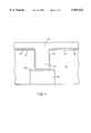
- an embodiment of the present inventioncomprises a semiconductor device having an interconnect pattern comprising wiring layer 10, representative of one of the conductive or metal layers in a multiple metal level semiconductor device. It should be understood that structure 10 is only a portion of many structures present on a semiconductor device.
- a dielectric interlayer 11separates different metal layers of a semiconductor device.
- Dielectric interlayer 11is typically formed of an oxide, such as silicon dioxide.
- oxidesuch as silicon dioxide.
- other materialssuch as low dielectric constant materials, e.g., polymers such as polyimides, as well as other non-conductive materials, can be employed for dielectric interlayer 11.
- Metal layer 10may comprise a barrier metal layer 10A, such as TiN, which can also function as an anti-reflection and/or electromigration/stress migration suppression layer overlying the actual metal.
- a barrier metal layer 10Asuch as TiN
- the presence of such a barrier layer 10Ais optional and, hence, omitted from the following figures for simplicity.
- a thin etch stop layer 12can optionally be applied on the upper surface of dielectric interlayer 11.
- Etch stop layer 12can also serve as a CMP stopping layer to avoid excessive polishing of dielectric interlayer 11.
- Etch stop layer 12is typically formed of an oxide material, such as silicon dioxide, a silicon nitride or a silicon oxynitride, and can be deposited in a conventional manner, as by CVD and may comprise silicon nitride.
- Opening 13is then formed in dielectric interlayer 11, and may serve as a contact or via opening or a trench opening. As one having ordinary skill in the art would recognize, if opening 13 is a contact opening, it would lead to an active region, such as a source/drain region formed in a semiconductor substrate rather than to conductive line 10. As illustrated, however, opening 13 constitutes a via opening.
- a seed layer 14comprising an alloy of a catalytically active metal, preferably Cu, and a refractory metal, preferably W or Ta, is deposited within opening 13 and on dielectric interlayer 11 or optional etch stop layer 12. Seed layer 14 exhibits superior step coverage and, hence, functions effectively as a catalyst for subsequent electroless deposition or electroplating of Cu or a Cu-base alloy thereon to form a reliable interconnection. Seed layer 14 also functions as a barrier layer to prevent diffusion of Cu ions, and an adhesion layer to prevent delamination of subsequently plated Cu or a Cu-base alloy. The seed layer can be sputter deposited or deposited by CVD to a suitable thickness, e.g., about 300 ⁇ to about 1000 ⁇ .
- Cu or a Cu alloysuch as Cu-base alloy, e.g., a CuNi, CuMg, CuSn, CuZn or CuPd alloy, 15 is electrolessly plated or electroplated on catalytic seed layer 14 filling via opening 13 forming a conductive plug 15, shown in FIG. 2, and forming a thin layer, e.g., up to about 1.5 microns, extending on dielectric interlayer 11.
- Cu-base alloye.g., a CuNi, CuMg, CuSn, CuZn or CuPd alloy
- the deposited Cu or Cu alloy layer 15is subjected to planarization, preferably by CMP, to remove the thin plated Cu or Cu-base alloy layer and seed layer 14 from the upper surface of dielectric interlayer 11.
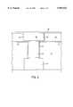
- a second dielectric interlayer 21is deposited on the planarized surface and a trench opening formed in communication with conductive plug 15.
- Another catalytically active Cu-refractory metal alloy seed layer 22is deposited in the trench opening in second dielectric interlayer 21 and on the upper surface of second dielectric interlayer 21.
- the trenchis filled with Cu or a Cu-base alloy by electroless plating or electroplating, thereby forming a conductive line 23 in electrical contact with plug 15.
- the upper surface of the deposited Cu or Cu-base alloyis then planarized, as by CMP, and a barrier layer 24, such as silicon nitride, deposited thereon.
- a barrier layer 24such as silicon nitride, deposited thereon.
- the openings in the dielectric interlayersare formed by conventional photolithographic and etching techniques. Contact openings are filled with Cu or a Cu-base alloy to establish electrical contact with an active region on a semiconductor substrate, e.g., a source/drain region. Via openings are filled with Cu or Cu-base alloy to establish electrical contact between metal layers on different levels. Trench openings are filled with Cu or a Cu-base alloy to form a conductive line.
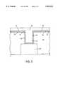
- FIG. 3Another embodiment of the present invention is illustrated in FIG. 3, wherein an initial barrier layer 30 is deposited in opening 13 and on dielectric interlayer 10 or optional etch stop layer 12, for additional prevention of Cu migration.
- Barrier layer 30can comprise a refractory metal, refractory metal alloy or refractory metal compound, preferably Ta, W or a nitride thereof.
- catalytic seed layer 14comprising an alloy of Cu and a refractory metal, is deposited on barrier layer 30 within opening 13 and on dielectric interlayer 11.
- Cu or a Cu-base alloy 15is then electrolessly plated or electroplated on Cu-refractory metal catalytic seed layer 14 filling opening 13 and forming a thin layer on dielectric interlayer 11.
- Subsequent processingthen continues in a manner similar to that illustrated in FIG. 2.
- FIGS. 4 and 5Another embodiment of the present invention is illustrated in FIGS. 4 and 5, wherein vias and trenches are simultaneously formed and filled.
- reference numeral 40represents a conductive line on which dielectric interlayer 41 is formed. Openings 42 and 43 are then formed in dielectric interlayer 41. Opening 43 is a trench opening while opening 42 comprises upper trench opening section 42A communicating with lower via opening section 42B, formed by a dual damascene technique, such as that disclosed in U.S. Pat. No. 4,789,648.
- etch stop layer 44formed on dielectric interlayer 41.
- catalytic seed layer 51comprising Cu and a refractory metal alloy, such as Ta, is deposited in openings 42 and 43.
- Catalytic seed layer 51although not shown in FIG. 5, is also formed during processing on optional etch stop layer 44, but removed during planarization.
- trench opening 43is filled to form conductive line 52.
- the lower via opening section 42B of opening 42is filled to form conductive plug 53 and, simultaneously, the upper trench opening section 42A of opening 42 is filled to form conductive line 54.
- Planarizationis then effected, as by CMP, and etch stop layer 55 deposited thereon.
- the present inventionhas been illustrated in terms of vias and trenches, the present invention can be readily extended to contact openings as well.
- the underlying regionwould not be a metal layer, but a doped contact region or silicide region of a contact.
- interconnect patterns implementing the present inventioncan extend to those conductive regions referred to as contacts.
- a catalytic seed layercomprising a Cu-refractory metal alloy exhibiting superior step coverage, is electrolessly plated or electroplated in openings, including high aspect ratio openings.
- the seed layeris oxidation resistant. Accordingly, it is not necessary to maintain the deposited seed layer under vacuum until Cu or a Cu-base alloy is plated thereon, although a vacuum can also be maintained during processing.
- the solutions employed in the present invention for electroless deposition of Cu or electroplating of Cu or a Cu alloyare conventional and, hence, not described herein in detail. It has been found particularly suitable to employ an electroless solution comprising copper sulfate to supply Cu 2+ cations, ethylenediaminetetraacetic acid (EDTA) as a complexing agent for Cu 2+ cations, quaternary ammonium hydroxides or potassium hydroxide (KOH) to supply the OH - ions, formaldehyde (HCHO) or glyoxylic acid as a reducing agent, RHODAFAC RE 610 or a polyethylene glycol as a surfactant and wetting agent, and ammonium cyanide or 2,2"-dipyridyl as a stabilizer and ductility promoter.
- an electroless solutioncomprising copper sulfate to supply Cu 2+ cations, ethylenediaminetetraacetic acid (EDTA) as a complexing agent for Cu 2+ cations
- Alloys (A) and (B) abovewere sputter deposited on the surface of a silicon oxide dielectric layer and served as catalytic seed/barrier layers.
- the resistivity of the sputter deposited film of Alloy Awas determined to be about 95 ⁇ cm.
- the resistivity of sputter deposited Alloy Bwas determined to be about 40 ⁇ cm.
- Cu filmswere then electroplated in a CUBATHTM acid plating bath on Alloy A and Alloy B. Pulse deposition techniques were used to plate Cu with a duty cycle of about 50-90%, at a frequency of about 10-1000 Hz and a cathodic current density amplitude of about 15-30 mA/cm 2 .
- the plated Cu films in both casesexhibited good adhesion, fine grain structures, low resistivities and good thickness uniformity.
- the resistivity of Cu films deposited on Alloy A and Alloy Bwere in the range of about 1.8 to 1.9 ⁇ cm with a thickness uniformity of about 5-7%, 1 ⁇ .
- Alloy A and Alloy Bas described in Example 1, were sputter deposited on the surface of a silicon oxide dielectric layer and served as catalytic seed/barrier layers.
- Cu filmswere electrolessly plated on sputter deposited Alloy A and sputter deposited Alloy B.
- Electroless platingwas conducted at a deposition temperature of about 50° C. to about 80° C. employing plating baths containing about 5-10 g/l CuSO 4 ⁇ 5H 2 O, about 10-70 g/l EDTA, about 5-10 ml/l (about 37% solution) HCHO, with a pH of about 11.8-13.3.
- the plated Cu filmexhibited good adhesion, a fine grain structure, low resistivity and good thickness uniformity.
- the resistivity and thickness uniformity of electrolessly plated Cu films on Cu--Ta seed/barrier layerswere about the same as for the electroplated films of Example 1.
- the present inventioncomprises a conventional semiconductor substrate, such as monocrystalline silicon, and conventional dielectric layers, such as silicon dioxide layers, formed in a conventional manner as by thermal oxidation of a deposited silicon layer, PECVD, thermal enhanced CVD, spin-on techniques, and silicon dioxide derived from deposited tetraethyl orthosilicate (TEOS).
- PECVDplasma oxidation deposition
- CVDthermal enhanced CVD
- spin-on techniquesspin-on techniques
- silicon dioxide derived from deposited tetraethyl orthosilicate (TEOS)silicon dioxide derived from deposited tetraethyl orthosilicate
- interconnect patterns of the present inventioncomprising Cu or a Cu-base alloy electrolessly plated or electroplated enjoy the advantages associated with Cu for conductive paths in a semiconductor device.
- the present inventionis not limited to the size of the device or openings, but can advantageously be applied for submicron technology, particularly wherein openings are formed with high aspect ratios. Electroless plating or electroplating can be performed as a batch process in which a substantial number of wafers are immersed in a wet bath at the same time.
- the present inventionprovides a cost effective, efficient technique for forming a high conductivity interconnect pattern with high reliability by electroplating or electrolessly plating Cu or a Cu-base alloy on a seed layer comprising an alloy of Cu and a refractory metal, such as Ta or W.
- interconnection patternsare reliably formed with filled openings for contacts and vias having an aspect ratio of 4:1 and greater, and filled trench openings having a contact aspect ratio of about 2:1 and greater.
- the use of a Cu-refractory metal alloy seed layeradvantageously provides superior step coverage, thereby ensuring reliability, serves as a barrier layer and provides superior adhesion.
- An initial barrier layercomprising a refractory metal, alloy or compound thereof, can also be initially deposited, and the Cu-refractory metal alloy seed layer deposited thereon.
Landscapes
- Engineering & Computer Science (AREA)
- Physics & Mathematics (AREA)
- Condensed Matter Physics & Semiconductors (AREA)
- General Physics & Mathematics (AREA)
- Computer Hardware Design (AREA)
- Microelectronics & Electronic Packaging (AREA)
- Power Engineering (AREA)
- Manufacturing & Machinery (AREA)
- Internal Circuitry In Semiconductor Integrated Circuit Devices (AREA)
Abstract
Description
______________________________________ (Alloy A) (Alloy B) ______________________________________ Cu . . . about 20 at. % Cu . . . about 80 at. % Ta . . . about 80 at. % Ta . . . about 20 at. % ______________________________________
Claims (37)
Priority Applications (1)
| Application Number | Priority Date | Filing Date | Title |
|---|---|---|---|
| US08/857,129US5969422A (en) | 1997-05-15 | 1997-05-15 | Plated copper interconnect structure |
Applications Claiming Priority (1)
| Application Number | Priority Date | Filing Date | Title |
|---|---|---|---|
| US08/857,129US5969422A (en) | 1997-05-15 | 1997-05-15 | Plated copper interconnect structure |
Publications (1)
| Publication Number | Publication Date |
|---|---|
| US5969422Atrue US5969422A (en) | 1999-10-19 |
Family
ID=25325254
Family Applications (1)
| Application Number | Title | Priority Date | Filing Date |
|---|---|---|---|
| US08/857,129Expired - LifetimeUS5969422A (en) | 1997-05-15 | 1997-05-15 | Plated copper interconnect structure |
Country Status (1)
| Country | Link |
|---|---|
| US (1) | US5969422A (en) |
Cited By (446)
| Publication number | Priority date | Publication date | Assignee | Title |
|---|---|---|---|---|
| US6040243A (en)* | 1999-09-20 | 2000-03-21 | Chartered Semiconductor Manufacturing Ltd. | Method to form copper damascene interconnects using a reverse barrier metal scheme to eliminate copper diffusion |
| US6066892A (en)* | 1997-05-08 | 2000-05-23 | Applied Materials, Inc. | Copper alloy seed layer for copper metallization in an integrated circuit |
| US6080656A (en)* | 1999-09-01 | 2000-06-27 | Taiwan Semiconductor Manufacturing Company | Method for forming a self-aligned copper structure with improved planarity |
| US6096648A (en)* | 1999-01-26 | 2000-08-01 | Amd | Copper/low dielectric interconnect formation with reduced electromigration |
| US6100196A (en)* | 1996-04-08 | 2000-08-08 | Chartered Semiconductor Manufacturing Ltd. | Method of making a copper interconnect with top barrier layer |
| US6103624A (en)* | 1999-04-15 | 2000-08-15 | Advanced Micro Devices, Inc. | Method of improving Cu damascene interconnect reliability by laser anneal before barrier polish |
| US6110826A (en)* | 1998-06-08 | 2000-08-29 | Industrial Technology Research Institute | Dual damascene process using selective W CVD |
| US6147000A (en)* | 1998-08-11 | 2000-11-14 | Advanced Micro Devices, Inc. | Method for forming low dielectric passivation of copper interconnects |
| US6156655A (en)* | 1999-09-30 | 2000-12-05 | United Microelectronics Corp. | Retardation layer for preventing diffusion of metal layer and fabrication method thereof |
| US6159853A (en)* | 1999-08-04 | 2000-12-12 | Industrial Technology Research Institute | Method for using ultrasound for assisting forming conductive layers on semiconductor devices |
| US6169028B1 (en)* | 1999-01-26 | 2001-01-02 | United Microelectronics Corp. | Method fabricating metal interconnected structure |
| US6181013B1 (en)* | 1999-06-25 | 2001-01-30 | Taiwan Semiconductor Manufacturing Company | Method for selective growth of Cu3Ge or Cu5Si for passivation of damascene copper structures and device manufactured thereby |
| US6181012B1 (en)* | 1998-04-27 | 2001-01-30 | International Business Machines Corporation | Copper interconnection structure incorporating a metal seed layer |
| US6197688B1 (en)* | 1998-02-12 | 2001-03-06 | Motorola Inc. | Interconnect structure in a semiconductor device and method of formation |
| US6211068B1 (en)* | 1999-05-25 | 2001-04-03 | United Microelectronics Corp. | Dual damascene process for manufacturing interconnects |
| US6211049B1 (en) | 1998-09-10 | 2001-04-03 | Micron Technology, Inc. | Forming submicron integrated-circuit wiring from gold, silver, copper, and other metals |
| US6221765B1 (en)* | 1998-08-31 | 2001-04-24 | Nec Corporation | Method for manufacturing a semiconductor device |
| US6221763B1 (en)* | 1999-04-05 | 2001-04-24 | Micron Technology, Inc. | Method of forming a metal seed layer for subsequent plating |
| US6225223B1 (en)* | 1999-08-16 | 2001-05-01 | Taiwan Semiconductor Manufacturing Company | Method to eliminate dishing of copper interconnects |
| US6225681B1 (en)* | 1999-09-07 | 2001-05-01 | Conexant Systems, Inc. | Microelectronic interconnect structures and methods for forming the same |
| US6242808B1 (en)* | 1998-04-09 | 2001-06-05 | Fujitsu Limited | Semiconductor device with copper wiring and semiconductor device manufacturing method |
| US6251770B1 (en)* | 1999-06-30 | 2001-06-26 | Lam Research Corp. | Dual-damascene dielectric structures and methods for making the same |
| US6268289B1 (en)* | 1998-05-18 | 2001-07-31 | Motorola Inc. | Method for protecting the edge exclusion of a semiconductor wafer from copper plating through use of an edge exclusion masking layer |
| US6277755B1 (en)* | 1999-12-20 | 2001-08-21 | United Microelectronics Corp. | Method for fabricating an interconnect |
| US6284656B1 (en) | 1998-08-04 | 2001-09-04 | Micron Technology, Inc. | Copper metallurgy in integrated circuits |
| EP1130654A1 (en)* | 2000-03-01 | 2001-09-05 | Infineon Technologies AG | Integrated device including a metal- insulator-metal capacitor |
| US6291082B1 (en)* | 2000-06-13 | 2001-09-18 | Advanced Micro Devices, Inc. | Method of electroless ag layer formation for cu interconnects |
| US6294467B1 (en)* | 1998-03-18 | 2001-09-25 | Nec Corporation | Process for forming fine wiring |
| US6294462B1 (en)* | 1997-12-22 | 2001-09-25 | Hyundai Electronics Industries Co., Ltd. | Manufacturing method of interconnection layer for semiconductor device |
| US6297154B1 (en)* | 1998-08-28 | 2001-10-02 | Agere System Guardian Corp. | Process for semiconductor device fabrication having copper interconnects |
| US20010026952A1 (en)* | 1998-09-23 | 2001-10-04 | Manfred Engelhardt | Integrated circuit configuration and production method |
| US6303498B1 (en)* | 1999-08-20 | 2001-10-16 | Taiwan Semiconductor Manufacturing Company | Method for preventing seed layer oxidation for high aspect gap fill |
| US6303486B1 (en)* | 2000-01-28 | 2001-10-16 | Advanced Micro Devices, Inc. | Method of fabricating copper-based semiconductor devices using a sacrificial dielectric layer and an unconstrained copper anneal |
| US6313028B2 (en)* | 1999-03-05 | 2001-11-06 | United Microelectronics Corp. | Method of fabricating dual damascene structure |
| US6316351B1 (en) | 2000-05-31 | 2001-11-13 | Taiwan Semiconductor Manufacturing Company | Inter-metal dielectric film composition for dual damascene process |
| US6326306B1 (en)* | 2001-02-15 | 2001-12-04 | United Microelectronics Corp. | Method of forming copper dual damascene structure |
| US6329701B1 (en)* | 1999-10-04 | 2001-12-11 | Advanced Micro Devices, Inc. | Semiconductor device comprising copper interconnects with reduced in-line diffusion |
| US6339029B1 (en)* | 2000-01-19 | 2002-01-15 | Taiwan Semiconductor Manufacturing Company | Method to form copper interconnects |
| US6340633B1 (en)* | 1999-03-26 | 2002-01-22 | Advanced Micro Devices, Inc. | Method for ramped current density plating of semiconductor vias and trenches |
| US6344125B1 (en)* | 2000-04-06 | 2002-02-05 | International Business Machines Corporation | Pattern-sensitive electrolytic metal plating |
| US6350364B1 (en)* | 2000-02-18 | 2002-02-26 | Taiwan Semiconductor Manufacturing Company | Method for improvement of planarity of electroplated copper |
| US6352917B1 (en)* | 2000-06-21 | 2002-03-05 | Chartered Semiconductor Manufacturing Ltd. | Reversed damascene process for multiple level metal interconnects |
| US6355562B1 (en)* | 1998-07-01 | 2002-03-12 | Advanced Technology Materials, Inc. | Adhesion promotion method for CVD copper metallization in IC applications |
| US6355983B2 (en)* | 1997-05-20 | 2002-03-12 | Texas Instruments Incorporated | Surface modified interconnects |
| US6358848B1 (en)* | 2000-11-30 | 2002-03-19 | Advanced Micro Devices, Inc. | Method of reducing electromigration in copper lines by forming an interim layer of calcium-doped copper seed layer in a chemical solution and semiconductor device thereby formed |
| US6362099B1 (en)* | 1999-03-09 | 2002-03-26 | Applied Materials, Inc. | Method for enhancing the adhesion of copper deposited by chemical vapor deposition |
| US6365502B1 (en) | 1998-12-22 | 2002-04-02 | Cvc Products, Inc. | Microelectronic interconnect material with adhesion promotion layer and fabrication method |
| US6376368B1 (en)* | 1999-08-05 | 2002-04-23 | Samsung Electronics Co., Ltd. | Method of forming contact structure in a semiconductor device |
| US20020048935A1 (en)* | 1998-08-28 | 2002-04-25 | Kabushiki Kaisha Toshiba | Semiconductor device and method for manufacturing the same |
| US20020050459A1 (en)* | 2000-11-02 | 2002-05-02 | Kabushiki Kaisha Toshiba | Electronic device manufacturing method |
| US6387821B1 (en)* | 1998-10-05 | 2002-05-14 | Nec Corporation | Method of manufacturing a semiconductor device |
| US6391776B1 (en)* | 1999-01-08 | 2002-05-21 | Applied Materials, Inc. | Method of depositing a copper seed layer which promotes improved feature surface coverage |
| US6400031B1 (en)* | 1998-06-11 | 2002-06-04 | Oki Electric Industry Co., Ltd. | Semiconductor device having damascene interconnection structure that prevents void formation between interconnections |
| US20020074233A1 (en)* | 1998-02-04 | 2002-06-20 | Semitool, Inc. | Method and apparatus for low temperature annealing of metallization micro-structures in the production of a microelectronic device |
| US6426289B1 (en)* | 2000-03-24 | 2002-07-30 | Micron Technology, Inc. | Method of fabricating a barrier layer associated with a conductor layer in damascene structures |
| US6437441B1 (en)* | 1997-07-10 | 2002-08-20 | Kawasaki Microelectronics, Inc. | Wiring structure of a semiconductor integrated circuit and a method of forming the wiring structure |
| US20020114745A1 (en)* | 2001-01-08 | 2002-08-22 | Elliott David J. | Photocatalytic reactor system for treating flue effluents |
| US6440854B1 (en)* | 2001-02-02 | 2002-08-27 | Novellus Systems, Inc. | Anti-agglomeration of copper seed layers in integrated circuit metalization |
| US6444263B1 (en) | 2000-09-15 | 2002-09-03 | Cvc Products, Inc. | Method of chemical-vapor deposition of a material |
| US6455425B1 (en)* | 2000-01-18 | 2002-09-24 | Advanced Micro Devices, Inc. | Selective deposition process for passivating top interface of damascene-type Cu interconnect lines |
| US6455938B1 (en)* | 2001-07-13 | 2002-09-24 | Advanced Micro Devices, Inc. | Integrated circuit interconnect shunt layer |
| US6465334B1 (en) | 2000-10-05 | 2002-10-15 | Advanced Micro Devices, Inc. | Enhanced electroless deposition of dielectric precursor materials for use in in-laid gate MOS transistors |
| US6465376B2 (en)* | 1999-08-18 | 2002-10-15 | International Business Machines Corporation | Method and structure for improving electromigration of chip interconnects |
| US6479389B1 (en)* | 1999-10-04 | 2002-11-12 | Taiwan Semiconductor Manufacturing Company | Method of doping copper metallization |
| US20020170173A1 (en)* | 2001-05-21 | 2002-11-21 | Shinko Electric Industries Co., Ltd. | Method of production of circuit board, semiconductor device, and plating system |
| US6492270B1 (en) | 2001-03-19 | 2002-12-10 | Taiwan Semiconductor Manufacturing Company | Method for forming copper dual damascene |
| US6498093B1 (en)* | 2002-01-17 | 2002-12-24 | Advanced Micro Devices, Inc. | Formation without vacuum break of sacrificial layer that dissolves in acidic activation solution within interconnect |
| KR100365643B1 (en)* | 2000-10-09 | 2002-12-26 | 삼성전자 주식회사 | Method for forming damascene interconnection of semiconductor device and damascene interconnection fabricated thereby |
| US6503375B1 (en) | 2000-02-11 | 2003-01-07 | Applied Materials, Inc | Electroplating apparatus using a perforated phosphorus doped consumable anode |
| US6506668B1 (en) | 2001-06-22 | 2003-01-14 | Advanced Micro Devices, Inc. | Utilization of annealing enhanced or repaired seed layer to improve copper interconnect reliability |
| US20030010645A1 (en)* | 2001-06-14 | 2003-01-16 | Mattson Technology, Inc. | Barrier enhancement process for copper interconnects |
| US6509262B1 (en)* | 2000-11-30 | 2003-01-21 | Advanced Micro Devices, Inc. | Method of reducing electromigration in copper lines by calcium-doping copper surfaces in a chemical solution |
| US6512281B2 (en)* | 1998-04-08 | 2003-01-28 | Nec Corporation | Method of forming a semiconductor device and an improved deposition system |
| US6531777B1 (en)* | 2000-06-22 | 2003-03-11 | Advanced Micro Devices, Inc. | Barrier metal integrity testing using a dual level line to line leakage testing pattern and partial CMP |
| US6554914B1 (en) | 2001-02-02 | 2003-04-29 | Novellus Systems, Inc. | Passivation of copper in dual damascene metalization |
| US6559051B1 (en) | 2000-10-05 | 2003-05-06 | Advanced Micro Devices, Inc. | Electroless deposition of dielectric precursor materials for use in in-laid gate MOS transistors |
| US6566211B2 (en) | 1997-06-11 | 2003-05-20 | Texas Instruments Incorporated | Surface modified interconnects |
| US6565729B2 (en) | 1998-03-20 | 2003-05-20 | Semitool, Inc. | Method for electrochemically depositing metal on a semiconductor workpiece |
| WO2002045155A3 (en)* | 2000-11-29 | 2003-06-05 | Intel Corp | ELECTROLESS METHOD OF SEED LAYER DEPOSITION, REPAIR, AND FABRICATION OF Cu INTERCONNECTS |
| US6589874B2 (en)* | 1998-12-03 | 2003-07-08 | International Business Machines Corporation | Method for forming electromigration-resistant structures by doping |
| US20030129828A1 (en)* | 1999-10-02 | 2003-07-10 | Uri Cohen | Methods for making multiple seed layers for metallic interconnects |
| US6596149B2 (en)* | 1998-06-08 | 2003-07-22 | Samsung Electronics Co., Ltd. | Manufacturing method for capacitor having electrode formed by electroplating |
| US6600229B2 (en)* | 2001-01-23 | 2003-07-29 | Honeywell International Inc. | Planarizers for spin etch planarization of electronic components |
| US20030140988A1 (en)* | 2002-01-28 | 2003-07-31 | Applied Materials, Inc. | Electroless deposition method over sub-micron apertures |
| US20030141194A1 (en)* | 1998-03-20 | 2003-07-31 | Chen Linlin | Apparatus and method for electrolytically depositing copper on a semiconductor workpiece |
| US6624074B1 (en)* | 2000-11-30 | 2003-09-23 | Advanced Micro Devices, Inc. | Method of fabricating a semiconductor device by calcium doping a copper surface using a chemical solution |
| US6624070B2 (en)* | 2000-10-24 | 2003-09-23 | Shipley Company, L.L.C. | Plating catalysts |
| US6624515B1 (en)* | 2002-03-11 | 2003-09-23 | Micron Technology, Inc. | Microelectronic die including low RC under-layer interconnects |
| US6624513B1 (en)* | 1999-01-13 | 2003-09-23 | Hitachi, Ltd. | Semiconductor device with multilayer conductive structure formed on a semiconductor substrate |
| US6627995B2 (en)* | 2000-03-03 | 2003-09-30 | Cvc Products, Inc. | Microelectronic interconnect material with adhesion promotion layer and fabrication method |
| US20030189026A1 (en)* | 2002-04-03 | 2003-10-09 | Deenesh Padhi | Electroless deposition method |
| US20030190812A1 (en)* | 2002-04-03 | 2003-10-09 | Deenesh Padhi | Electroless deposition method |
| US6633083B2 (en)* | 2000-02-28 | 2003-10-14 | Advanced Micro Devices Inc. | Barrier layer integrity test |
| US20030201537A1 (en)* | 2002-04-26 | 2003-10-30 | International Business Machines Corporation | Barrier material for copper structures |
| US6645550B1 (en) | 2000-06-22 | 2003-11-11 | Applied Materials, Inc. | Method of treating a substrate |
| US6664122B1 (en) | 2001-10-19 | 2003-12-16 | Novellus Systems, Inc. | Electroless copper deposition method for preparing copper seed layers |
| US6663787B1 (en)* | 2001-02-06 | 2003-12-16 | Advanced Micro Devices, Inc. | Use of ta/tan for preventing copper contamination of low-k dielectric layers |
| US20040004288A1 (en)* | 2000-08-24 | 2004-01-08 | Matsushita Electric Industrial Co., Ltd. | Semiconductor device and manufacturing method of the same |
| US20040014312A1 (en)* | 2002-07-08 | 2004-01-22 | Nec Electronics Corporation | Semiconductor device and manufacturing method thereof |
| US20040026754A1 (en)* | 2002-08-07 | 2004-02-12 | Peikang Liu | Radio frequency identification device and method |
| US6696746B1 (en) | 1998-04-29 | 2004-02-24 | Micron Technology, Inc. | Buried conductors |
| US20040038052A1 (en)* | 2002-08-21 | 2004-02-26 | Collins Dale W. | Microelectronic workpiece for electrochemical deposition processing and methods of manufacturing and using such microelectronic workpieces |
| US20040041264A1 (en)* | 2002-08-27 | 2004-03-04 | Kloster Grant M. | Method for alloy-electroplating group IB metals with refractory metals for interconnections |
| US6703308B1 (en) | 2001-11-26 | 2004-03-09 | Advanced Micro Devices, Inc. | Method of inserting alloy elements to reduce copper diffusion and bulk diffusion |
| US6703307B2 (en) | 2001-11-26 | 2004-03-09 | Advanced Micro Devices, Inc. | Method of implantation after copper seed deposition |
| US20040053446A1 (en)* | 1998-04-17 | 2004-03-18 | Nec Electronics Corporation | Semiconductor device and manufacturing method of the same |
| US20040087141A1 (en)* | 2002-10-30 | 2004-05-06 | Applied Materials, Inc. | Post rinse to improve selective deposition of electroless cobalt on copper for ULSI application |
| US20040087171A1 (en)* | 1999-10-02 | 2004-05-06 | Uri Cohen | Combined conformal/non-conformal seed layers for metallic interconnects |
| US20040089948A1 (en)* | 2002-11-07 | 2004-05-13 | Yu-Ting Cheng | Technology for fabrication of packaging interface substrate wafers with fully metallized vias through the substrate wafer |
| US6743716B2 (en) | 2000-01-18 | 2004-06-01 | Micron Technology, Inc. | Structures and methods to enhance copper metallization |
| US20040108217A1 (en)* | 2002-12-05 | 2004-06-10 | Dubin Valery M. | Methods for forming copper interconnect structures by co-plating of noble metals and structures formed thereby |
| US6753251B2 (en) | 1998-02-04 | 2004-06-22 | Semitool, Inc. | Method for filling recessed micro-structures with metallization in the production of a microelectronic device |
| US6756682B2 (en) | 2002-05-29 | 2004-06-29 | Micron Technology, Inc. | High aspect ratio fill method and resulting structure |
| US6756298B2 (en) | 2000-01-18 | 2004-06-29 | Micron Technology, Inc. | Methods and apparatus for making integrated-circuit wiring from copper, silver, gold, and other metals |
| US20040145062A1 (en)* | 2003-01-23 | 2004-07-29 | Markus Nopper | Method of forming a metal layer over patterned dielectric by electroless deposition using a catalyst |
| US20040152295A1 (en)* | 2003-02-03 | 2004-08-05 | International Business Machines Corporation | Sacrificial metal liner for copper |
| US20040157431A1 (en)* | 2003-02-10 | 2004-08-12 | Taiwan Semiconductor Manufacturing Company | Barrier free copper interconnect by multi-layer copper seed |
| WO2004068576A3 (en)* | 2003-01-23 | 2004-09-10 | Advanced Micro Devices Inc | Method of forming a catalyst containing layer over a patterned dielectric |
| US20040191977A1 (en)* | 2001-10-05 | 2004-09-30 | Taiwan Semiconductor Manufacturing Company | Composite etching stop in semiconductor process integration |
| US20040200061A1 (en)* | 2003-04-11 | 2004-10-14 | Coleman James P. | Conductive pattern and method of making |
| US6811675B2 (en) | 1998-03-20 | 2004-11-02 | Semitool, Inc. | Apparatus and method for electrolytically depositing copper on a semiconductor workpiece |
| US6812143B2 (en)* | 2002-04-26 | 2004-11-02 | International Business Machines Corporation | Process of forming copper structures |
| US20040219738A1 (en)* | 2000-08-22 | 2004-11-04 | Dinesh Chopra | Method of providing a structure using self-aligned features |
| US6815336B1 (en)* | 1998-09-25 | 2004-11-09 | Taiwan Semiconductor Manufacturing Company, Ltd. | Planarization of copper damascene using reverse current electroplating and chemical mechanical polishing |
| US20040227243A1 (en)* | 2003-05-15 | 2004-11-18 | Dung-Ching Perng | Methods of pore sealing and metal encapsulation in porous low k interconnect |
| US20040232519A1 (en)* | 2001-08-14 | 2004-11-25 | Van Beek Jozef Thomas Martinus | Electronic device and method of testing and of manufacturing |
| US20040238961A1 (en)* | 2003-03-18 | 2004-12-02 | Cunningham James A. | Copper interconnect systems which use conductive, metal-based cap layers |
| US20040251550A1 (en)* | 2003-06-10 | 2004-12-16 | Takashi Yoda | Semiconductor device and method of manufacturing the same |
| US6835655B1 (en) | 2001-11-26 | 2004-12-28 | Advanced Micro Devices, Inc. | Method of implanting copper barrier material to improve electrical performance |
| US20050006777A1 (en)* | 2002-08-09 | 2005-01-13 | International Business Machines Corporation | Structure comprising an interlayer of palladium and/or platinum and method for fabrication thereof |
| US20050029665A1 (en)* | 2003-01-24 | 2005-02-10 | Taiwan Semiconductor Manufacturing Company, Ltd. | Barrier-less integration with copper alloy |
| US6861349B1 (en)* | 2002-05-15 | 2005-03-01 | Advanced Micro Devices, Inc. | Method of forming an adhesion layer with an element reactive with a barrier layer |
| US20050085031A1 (en)* | 2003-10-15 | 2005-04-21 | Applied Materials, Inc. | Heterogeneous activation layers formed by ionic and electroless reactions used for IC interconnect capping layers |
| US20050085073A1 (en)* | 2003-10-16 | 2005-04-21 | Advanced Micro Devices, Inc. | Method of using an adhesion precursor layer for chemical vapor deposition (CVD) copper deposition |
| US20050081785A1 (en)* | 2003-10-15 | 2005-04-21 | Applied Materials, Inc. | Apparatus for electroless deposition |
| US20050092611A1 (en)* | 2003-11-03 | 2005-05-05 | Semitool, Inc. | Bath and method for high rate copper deposition |
| US20050112856A1 (en)* | 2002-09-23 | 2005-05-26 | Dubin Valery M. | Seed layer treatment |
| US20050127516A1 (en)* | 2003-12-12 | 2005-06-16 | Mercer Betty S. | Small viatops for thick copper connectors |
| US20050127478A1 (en)* | 2003-12-10 | 2005-06-16 | Hiatt William M. | Microelectronic devices and methods for filling vias in microelectronic devices |
| US20050153548A1 (en)* | 2003-12-31 | 2005-07-14 | Dongbuanam Semiconductor Inc. | Method for fabricating semiconductor device to minimize terminal effect in ECP process |
| US6927160B1 (en)* | 1999-06-09 | 2005-08-09 | National Semiconductor Corporation | Fabrication of copper-containing region such as electrical interconnect |
| US20050186772A1 (en)* | 2004-02-03 | 2005-08-25 | Axel Brintzinger | Process for producing metallic interconnects and contact surfaces on electronic components |
| US6946065B1 (en)* | 1998-10-26 | 2005-09-20 | Novellus Systems, Inc. | Process for electroplating metal into microscopic recessed features |
| US20050218523A1 (en)* | 2004-03-30 | 2005-10-06 | Dubin Valery M | Integrated circuit with metal layer having carbon nanotubes and methods of making same |
| US20050269708A1 (en)* | 2001-01-17 | 2005-12-08 | Andricacos Panayotis C | Tungsten encapsulated copper interconnections using electroplating |
| US20050285272A1 (en)* | 1999-03-01 | 2005-12-29 | Micron Technology, Inc. | Conductive structures in integrated circuits |
| US20060001160A1 (en)* | 2003-05-16 | 2006-01-05 | Wen-Kai Wan | Surface treatment of metal interconnect lines |
| US20060003570A1 (en)* | 2003-12-02 | 2006-01-05 | Arulkumar Shanmugasundram | Method and apparatus for electroless capping with vapor drying |
| US6984891B2 (en) | 1998-02-27 | 2006-01-10 | Micron Technology, Inc. | Methods for making copper and other metal interconnections in integrated circuits |
| US20060006070A1 (en)* | 2004-07-09 | 2006-01-12 | International Business Machines Corporation | Copper conductor |
| US6995470B2 (en) | 2000-05-31 | 2006-02-07 | Micron Technology, Inc. | Multilevel copper interconnects with low-k dielectrics and air gaps |
| US20060046456A1 (en)* | 2004-08-25 | 2006-03-02 | Samsung Electronics Co., Ltd. | Damascene process using different kinds of metals |
| US20060063375A1 (en)* | 2004-09-20 | 2006-03-23 | Lsi Logic Corporation | Integrated barrier and seed layer for copper interconnect technology |
| US20060068181A1 (en)* | 2003-09-25 | 2006-03-30 | Dory Thomas S | Deep via seed repair using electroless plating chemistry |
| US20060071338A1 (en)* | 2004-09-30 | 2006-04-06 | International Business Machines Corporation | Homogeneous Copper Interconnects for BEOL |
| US20060084260A1 (en)* | 2004-09-07 | 2006-04-20 | Boyers David G | Copper processing using an ozone-solvent solution |
| US7041595B2 (en) | 1999-08-27 | 2006-05-09 | Micron Technology, Inc. | Method of forming a barrier seed layer with graded nitrogen composition |
| US7064065B2 (en) | 2003-10-15 | 2006-06-20 | Applied Materials, Inc. | Silver under-layers for electroless cobalt alloys |
| US7077860B2 (en) | 1997-04-24 | 2006-07-18 | Advanced Cardiovascular Systems, Inc. | Method of reducing or eliminating thrombus formation |
| US20060166448A1 (en)* | 1999-10-02 | 2006-07-27 | Uri Cohen | Apparatus for depositing seed layers |
| US7138014B2 (en) | 2002-01-28 | 2006-11-21 | Applied Materials, Inc. | Electroless deposition apparatus |
| US7148571B1 (en)* | 1999-07-30 | 2006-12-12 | Nec Electronics Corporation | Semiconductor device and method of manufacturing the same |
| US20070020931A1 (en)* | 2005-07-13 | 2007-01-25 | Fujitsu Limited | Manufacture method for semiconductor device having improved copper diffusion preventive function of plugs and wirings made of copper or copper alloy and semiconductor device of this kind |
| US20070035466A1 (en)* | 2003-04-11 | 2007-02-15 | Coleman James P | Conductive pattern and method of making |
| WO2006102182A3 (en)* | 2005-03-18 | 2007-03-01 | Applied Materials Inc | Process for electroless copper deposition |
| US20070045120A1 (en)* | 2005-09-01 | 2007-03-01 | Micron Technology, Inc. | Methods and apparatus for filling features in microfeature workpieces |
| US20070054488A1 (en)* | 2003-08-08 | 2007-03-08 | Ting-Chu Ko | Low resistance and reliable copper interconnects by variable doping |
| US20070062817A1 (en)* | 2005-09-20 | 2007-03-22 | Alchimer | Method of coating a surface of a substrate with a metal by electroplating |
| US20070062818A1 (en)* | 2005-09-20 | 2007-03-22 | Alchimer | Electroplating composition intended for coating a surface of a substrate with a metal |
| US7198675B2 (en) | 2003-09-30 | 2007-04-03 | Advanced Cardiovascular Systems | Stent mandrel fixture and method for selectively coating surfaces of a stent |
| US7205233B2 (en) | 2003-11-07 | 2007-04-17 | Applied Materials, Inc. | Method for forming CoWRe alloys by electroless deposition |
| US20070105377A1 (en)* | 2003-10-20 | 2007-05-10 | Novellus Systems, Inc. | Fabrication of semiconductor interconnect structure |
| US20070111519A1 (en)* | 2003-10-15 | 2007-05-17 | Applied Materials, Inc. | Integrated electroless deposition system |
| US7220665B2 (en) | 2003-08-05 | 2007-05-22 | Micron Technology, Inc. | H2 plasma treatment |
| US7232513B1 (en) | 2004-06-29 | 2007-06-19 | Novellus Systems, Inc. | Electroplating bath containing wetting agent for defect reduction |
| US20070166996A1 (en)* | 2006-01-17 | 2007-07-19 | International Business Machines Corporation | Method of making a semiconductor structure with a plating enhancement layer |
| US20070182521A1 (en)* | 2003-05-27 | 2007-08-09 | Megica Corporation | High performance system-on-chip inductor using post passivation process |
| US7258891B2 (en) | 2001-06-28 | 2007-08-21 | Advanced Cardiovascular Systems, Inc. | Stent mounting assembly and a method of using the same to coat a stent |
| US7262505B2 (en) | 2000-01-18 | 2007-08-28 | Micron Technology, Inc. | Selective electroless-plated copper metallization |
| US7270724B2 (en) | 2000-12-13 | 2007-09-18 | Uvtech Systems, Inc. | Scanning plasma reactor |
| US20070259456A1 (en)* | 2006-05-02 | 2007-11-08 | Formfactor, Inc. | Extended Probe Tips |
| US7297159B2 (en) | 2000-10-26 | 2007-11-20 | Advanced Cardiovascular Systems, Inc. | Selective coating of medical devices |
| US20070278684A1 (en)* | 1998-12-21 | 2007-12-06 | Mou-Shiung Lin | Top layers of metal for high performance IC's |
| US20080001269A1 (en)* | 2006-06-29 | 2008-01-03 | Hsu Rockwell M | Conductive interconnects along the edge of a microelectronic device |
| US20080000678A1 (en)* | 2006-06-30 | 2008-01-03 | Johnston Steven W | Integrating a bottomless via to promote adsorption of antisuppressor on exposed copper surface and enhance electroplating superfill on noble metals |
| US20080035972A1 (en)* | 1998-12-21 | 2008-02-14 | Megica Corporation | High performance system-on-chip using post passivation process |
| US20080037181A1 (en)* | 2006-08-08 | 2008-02-14 | Tdk Corporation | Method of forming plating film, method of manufacturing magnetic device and method of manufacturing perpendicular magnetic recording head |
| US7332428B2 (en) | 2005-02-28 | 2008-02-19 | Infineon Technologies Ag | Metal interconnect structure and method |
| US7338908B1 (en) | 2003-10-20 | 2008-03-04 | Novellus Systems, Inc. | Method for fabrication of semiconductor interconnect structure with reduced capacitance, leakage current, and improved breakdown voltage |
| US20080054444A1 (en)* | 2006-08-31 | 2008-03-06 | Micron Technology, Inc. | Microfeature workpieces having interconnects and conductive backplanes, and associated systems and methods |
| US20080081473A1 (en)* | 2006-09-28 | 2008-04-03 | Tokyo Electron Limited | Method for integrated substrate processing in copper metallization |
| US20080122109A1 (en)* | 2006-07-19 | 2008-05-29 | International Business Machines Corporation | Porous and dense hybrid interconnect structure and method of manufacture |
| US7381638B1 (en) | 1999-06-09 | 2008-06-03 | National Semiconductor Corporation | Fabrication technique using sputter etch and vacuum transfer |
| US20080164613A1 (en)* | 2007-01-10 | 2008-07-10 | International Business Machines Corporation | ULTRA-THIN Cu ALLOY SEED FOR INTERCONNECT APPLICATION |
| US7399713B2 (en) | 1998-03-13 | 2008-07-15 | Semitool, Inc. | Selective treatment of microelectric workpiece surfaces |
| US7402516B2 (en) | 2000-01-18 | 2008-07-22 | Micron Technology, Inc. | Method for making integrated circuits |
| US20080191352A1 (en)* | 2007-02-13 | 2008-08-14 | Chen-Hua Yu | Stacked contact with low aspect ratio |
| US20080206978A1 (en)* | 2007-02-28 | 2008-08-28 | Louis Lu-Chen Hsu | Electronic fuses in semiconductor integrated circuits |
| US20080280151A1 (en)* | 2006-10-05 | 2008-11-13 | Stmicroelectronics Crolles 2 Sas | Copper diffusion barrier |
| US7456102B1 (en)* | 2005-10-11 | 2008-11-25 | Novellus Systems, Inc. | Electroless copper fill process |
| US20090001511A1 (en)* | 2005-03-29 | 2009-01-01 | Megica Corporation | High performance system-on-chip using post passivation process |
| US20090057912A1 (en)* | 2007-08-31 | 2009-03-05 | Micron Technology, Inc. | Partitioned through-layer via and associated systems and methods |
| US7510634B1 (en) | 2006-11-10 | 2009-03-31 | Novellus Systems, Inc. | Apparatus and methods for deposition and/or etch selectivity |
| US7514353B2 (en) | 2005-03-18 | 2009-04-07 | Applied Materials, Inc. | Contact metallization scheme using a barrier layer over a silicide layer |
| US20090140429A1 (en)* | 2007-11-29 | 2009-06-04 | Kyu-Ha Lee | Metal interconnection of a semiconductor device and method of manufacturing the same |
| US20090148677A1 (en)* | 2007-12-10 | 2009-06-11 | International Business Machines Corporation | High aspect ratio electroplated metal feature and method |
| US7553377B1 (en) | 2004-04-27 | 2009-06-30 | Advanced Cardiovascular Systems, Inc. | Apparatus and method for electrostatic coating of an abluminal stent surface |
| US20090166869A1 (en)* | 2007-12-27 | 2009-07-02 | Dongbu Hitek Co., Ltd. | Semiconductor device and method of forming metal interconnection layer thereof |
| US7563324B1 (en) | 2003-12-29 | 2009-07-21 | Advanced Cardiovascular Systems Inc. | System and method for coating an implantable medical device |
| US7605082B1 (en) | 2005-10-13 | 2009-10-20 | Novellus Systems, Inc. | Capping before barrier-removal IC fabrication method |
| US7629249B2 (en) | 2006-08-28 | 2009-12-08 | Micron Technology, Inc. | Microfeature workpieces having conductive interconnect structures formed by chemically reactive processes, and associated systems and methods |
| US7632307B2 (en) | 2004-12-16 | 2009-12-15 | Advanced Cardiovascular Systems, Inc. | Abluminal, multilayer coating constructs for drug-delivery stents |
| US20100003539A1 (en)* | 2007-07-31 | 2010-01-07 | Atsushi Yabe | Plated article having metal thin film formed by electroless plating, and manufacturing method thereof |
| US7645696B1 (en) | 2006-06-22 | 2010-01-12 | Novellus Systems, Inc. | Deposition of thin continuous PVD seed layers having improved adhesion to the barrier layer |
| US20100009530A1 (en)* | 2007-03-27 | 2010-01-14 | Fujitsu Microelectronics Limited | Semiconductor device fabrication method |
| US20100015805A1 (en)* | 2003-10-20 | 2010-01-21 | Novellus Systems, Inc. | Wet Etching Methods for Copper Removal and Planarization in Semiconductor Processing |
| US7651934B2 (en) | 2005-03-18 | 2010-01-26 | Applied Materials, Inc. | Process for electroless copper deposition |
| US7654221B2 (en) | 2003-10-06 | 2010-02-02 | Applied Materials, Inc. | Apparatus for electroless deposition of metals onto semiconductor substrates |
| US20100029088A1 (en)* | 2003-10-20 | 2010-02-04 | Novellus Systems, Inc. | Modulated metal removal using localized wet etching |
| US7659203B2 (en) | 2005-03-18 | 2010-02-09 | Applied Materials, Inc. | Electroless deposition process on a silicon contact |
| US7659197B1 (en) | 2007-09-21 | 2010-02-09 | Novellus Systems, Inc. | Selective resputtering of metal seed layers |
| US7682966B1 (en) | 2007-02-01 | 2010-03-23 | Novellus Systems, Inc. | Multistep method of depositing metal seed layers |
| US7683458B2 (en) | 2004-09-02 | 2010-03-23 | Micron Technology, Inc. | Through-wafer interconnects for photoimager and memory wafers |
| US7696092B2 (en) | 2001-11-26 | 2010-04-13 | Globalfoundries Inc. | Method of using ternary copper alloy to obtain a low resistance and large grain size interconnect |
| US20100096273A1 (en)* | 2008-01-15 | 2010-04-22 | Applied Materials, Inc. | Cu surface plasma treatment to improve gapfill window |
| US7732314B1 (en) | 2001-03-13 | 2010-06-08 | Novellus Systems, Inc. | Method for depositing a diffusion barrier for copper interconnect applications |
| US20100147679A1 (en)* | 2008-12-17 | 2010-06-17 | Novellus Systems, Inc. | Electroplating Apparatus with Vented Electrolyte Manifold |
| US7749899B2 (en) | 2006-06-01 | 2010-07-06 | Micron Technology, Inc. | Microelectronic workpieces and methods and systems for forming interconnects in microelectronic workpieces |
| US20100193957A1 (en)* | 1998-02-23 | 2010-08-05 | Tomio Iwasaki | Semiconductor device and method for producing the same |
| US7781327B1 (en) | 2001-03-13 | 2010-08-24 | Novellus Systems, Inc. | Resputtering process for eliminating dielectric damage |
| US7795134B2 (en) | 2005-06-28 | 2010-09-14 | Micron Technology, Inc. | Conductive interconnect structures and formation methods using supercritical fluids |
| US20100273324A1 (en)* | 2004-06-18 | 2010-10-28 | Taiwan Semiconductor Manufacturing Company, Ltd. | Methods of manufacturing metal-silicide features |
| US20100279002A1 (en)* | 2004-08-09 | 2010-11-04 | Lam Research Corporation | Systems and Methods Affecting Profiles of Solutions Dispensed Across Microelectronic Topographies During Electroless Plating Processes |
| US7827930B2 (en) | 2004-01-26 | 2010-11-09 | Applied Materials, Inc. | Apparatus for electroless deposition of metals onto semiconductor substrates |
| US7842605B1 (en) | 2003-04-11 | 2010-11-30 | Novellus Systems, Inc. | Atomic layer profiling of diffusion barrier and metal seed layers |
| US7855147B1 (en) | 2006-06-22 | 2010-12-21 | Novellus Systems, Inc. | Methods and apparatus for engineering an interface between a diffusion barrier layer and a seed layer |
| US7863187B2 (en) | 2005-09-01 | 2011-01-04 | Micron Technology, Inc. | Microfeature workpieces and methods for forming interconnects in microfeature workpieces |
| US7867547B2 (en) | 2005-12-19 | 2011-01-11 | Advanced Cardiovascular Systems, Inc. | Selectively coating luminal surfaces of stents |
| US7867900B2 (en) | 2007-09-28 | 2011-01-11 | Applied Materials, Inc. | Aluminum contact integration on cobalt silicide junction |
| US20110006429A1 (en)* | 2009-07-08 | 2011-01-13 | Taiwan Semiconductor Manufacturing Company, Ltd. | Barrier layers for copper interconnect |
| US7884015B2 (en) | 2007-12-06 | 2011-02-08 | Micron Technology, Inc. | Methods for forming interconnects in microelectronic workpieces and microelectronic workpieces formed using such methods |
| US7897198B1 (en) | 2002-09-03 | 2011-03-01 | Novellus Systems, Inc. | Electroless layer plating process and apparatus |
| US7897516B1 (en) | 2007-05-24 | 2011-03-01 | Novellus Systems, Inc. | Use of ultra-high magnetic fields in resputter and plasma etching |
| US20110056913A1 (en)* | 2009-09-02 | 2011-03-10 | Mayer Steven T | Reduced isotropic etchant material consumption and waste generation |
| US7915736B2 (en) | 2005-09-01 | 2011-03-29 | Micron Technology, Inc. | Microfeature workpieces and methods for forming interconnects in microfeature workpieces |
| US7922880B1 (en) | 2007-05-24 | 2011-04-12 | Novellus Systems, Inc. | Method and apparatus for increasing local plasma density in magnetically confined plasma |
| US20110101529A1 (en)* | 2009-10-29 | 2011-05-05 | Taiwan Semiconductor Manufacturing Company, Ltd. | Barrier layer for copper interconnect |
| US20110124191A1 (en)* | 2003-05-09 | 2011-05-26 | Basf Aktiengesellschaft | Compositions for the currentless deposition of ternary materials for use in the semiconductor industry |
| US7960269B2 (en) | 2005-07-22 | 2011-06-14 | Megica Corporation | Method for forming a double embossing structure |
| US7973629B2 (en) | 2001-09-04 | 2011-07-05 | Megica Corporation | Method for making high-performance RF integrated circuits |
| US7972970B2 (en) | 2003-10-20 | 2011-07-05 | Novellus Systems, Inc. | Fabrication of semiconductor interconnect structure |
| US8003156B2 (en) | 2006-05-04 | 2011-08-23 | Advanced Cardiovascular Systems, Inc. | Rotatable support elements for stents |
| US8008775B2 (en) | 2004-09-09 | 2011-08-30 | Megica Corporation | Post passivation interconnection structures |
| US8018060B2 (en) | 2004-09-09 | 2011-09-13 | Megica Corporation | Post passivation interconnection process and structures |
| US8017523B1 (en) | 2008-05-16 | 2011-09-13 | Novellus Systems, Inc. | Deposition of doped copper seed layers having improved reliability |
| US8017237B2 (en) | 2006-06-23 | 2011-09-13 | Abbott Cardiovascular Systems, Inc. | Nanoshells on polymers |
| US8043484B1 (en) | 2001-03-13 | 2011-10-25 | Novellus Systems, Inc. | Methods and apparatus for resputtering process that improves barrier coverage |
| US8048441B2 (en) | 2007-06-25 | 2011-11-01 | Abbott Cardiovascular Systems, Inc. | Nanobead releasing medical devices |
| US8048448B2 (en) | 2006-06-15 | 2011-11-01 | Abbott Cardiovascular Systems Inc. | Nanoshells for drug delivery |
| US8089155B2 (en)* | 1998-12-21 | 2012-01-03 | Megica Corporation | High performance system-on-chip discrete components using post passivation process |
| US20120104471A1 (en)* | 2010-10-28 | 2012-05-03 | Taiwan Semiconductor Manufacturing Company, Ltd. | Contact structure for reducing gate resistance and method of making the same |
| US8178435B2 (en) | 1998-12-21 | 2012-05-15 | Megica Corporation | High performance system-on-chip inductor using post passivation process |
| US20120119269A1 (en)* | 2009-06-12 | 2012-05-17 | Ulvac, Inc. | Method for producing electronic device, electronic device, semiconductor device, and transistor |
| US8298933B2 (en) | 2003-04-11 | 2012-10-30 | Novellus Systems, Inc. | Conformal films on semiconductor substrates |
| US8322031B2 (en) | 2004-08-27 | 2012-12-04 | Micron Technology, Inc. | Method of manufacturing an interposer |
| US8361900B2 (en) | 2010-04-16 | 2013-01-29 | Taiwan Semiconductor Manufacturing Company, Ltd. | Barrier layer for copper interconnect |
| US8409960B2 (en) | 2011-04-08 | 2013-04-02 | Micron Technology, Inc. | Methods of patterning platinum-containing material |
| US20130084656A1 (en)* | 2011-09-29 | 2013-04-04 | Renesas Electronics Corporation | Method for manufacturing a semiconductor device |
| US8421158B2 (en) | 1998-12-21 | 2013-04-16 | Megica Corporation | Chip structure with a passive device and method for forming the same |
| US8470191B2 (en) | 2003-10-20 | 2013-06-25 | Novellus Systems, Inc. | Topography reduction and control by selective accelerator removal |
| US20130224887A1 (en)* | 2012-02-28 | 2013-08-29 | Dok Won Lee | Method of Forming a Laminated Magnetic Core with Sputter Deposited and Electroplated Layers |
| US20130252418A1 (en)* | 2012-03-23 | 2013-09-26 | International Business Machines Corporation | Electromigration-resistant lead-free solder interconnect structures |
| US20130277097A1 (en)* | 2010-12-27 | 2013-10-24 | Lg Innotek Co., Ltd. | Method for manufacturing printed circuit board |
| US8603530B2 (en) | 2006-06-14 | 2013-12-10 | Abbott Cardiovascular Systems Inc. | Nanoshell therapy |
| US20140029181A1 (en)* | 2012-07-27 | 2014-01-30 | Florian Gstrein | Interlayer interconnects and associated techniques and configurations |
| US8664562B2 (en) | 2004-05-05 | 2014-03-04 | Micron Technology, Inc. | Systems and methods for forming apertures in microfeature workpieces |
| US8679982B2 (en) | 2011-08-26 | 2014-03-25 | Applied Materials, Inc. | Selective suppression of dry-etch rate of materials containing both silicon and oxygen |
| US8679972B1 (en) | 2001-03-13 | 2014-03-25 | Novellus Systems, Inc. | Method of depositing a diffusion barrier for copper interconnect applications |
| US8679983B2 (en) | 2011-09-01 | 2014-03-25 | Applied Materials, Inc. | Selective suppression of dry-etch rate of materials containing both silicon and nitrogen |
| US8765574B2 (en) | 2012-11-09 | 2014-07-01 | Applied Materials, Inc. | Dry etch process |
| US8771539B2 (en) | 2011-02-22 | 2014-07-08 | Applied Materials, Inc. | Remotely-excited fluorine and water vapor etch |
| US8801952B1 (en) | 2013-03-07 | 2014-08-12 | Applied Materials, Inc. | Conformal oxide dry etch |
| US8808563B2 (en) | 2011-10-07 | 2014-08-19 | Applied Materials, Inc. | Selective etch of silicon by way of metastable hydrogen termination |
| US20140262468A1 (en)* | 2013-03-12 | 2014-09-18 | Taiwan Semiconductor Manufacturing Company, Ltd. | System and Method for an Improved Interconnect Structure |
| US8846163B2 (en) | 2004-02-26 | 2014-09-30 | Applied Materials, Inc. | Method for removing oxides |
| US8895449B1 (en) | 2013-05-16 | 2014-11-25 | Applied Materials, Inc. | Delicate dry clean |
| US20140352135A1 (en)* | 2013-05-30 | 2014-12-04 | Dyi-chung Hu | Circuit board structure with embedded fine-pitch wires and fabrication method thereof |
| US8921234B2 (en) | 2012-12-21 | 2014-12-30 | Applied Materials, Inc. | Selective titanium nitride etching |
| US8927390B2 (en) | 2011-09-26 | 2015-01-06 | Applied Materials, Inc. | Intrench profile |
| US8951429B1 (en) | 2013-10-29 | 2015-02-10 | Applied Materials, Inc. | Tungsten oxide processing |
| US8956980B1 (en) | 2013-09-16 | 2015-02-17 | Applied Materials, Inc. | Selective etch of silicon nitride |
| US8969212B2 (en) | 2012-11-20 | 2015-03-03 | Applied Materials, Inc. | Dry-etch selectivity |
| US8975152B2 (en) | 2011-11-08 | 2015-03-10 | Applied Materials, Inc. | Methods of reducing substrate dislocation during gapfill processing |
| US8980763B2 (en) | 2012-11-30 | 2015-03-17 | Applied Materials, Inc. | Dry-etch for selective tungsten removal |
| US8999856B2 (en) | 2011-03-14 | 2015-04-07 | Applied Materials, Inc. | Methods for etch of sin films |
| US9023732B2 (en) | 2013-03-15 | 2015-05-05 | Applied Materials, Inc. | Processing systems and methods for halide scavenging |
| US9023734B2 (en) | 2012-09-18 | 2015-05-05 | Applied Materials, Inc. | Radical-component oxide etch |
| US9028666B2 (en) | 2011-05-17 | 2015-05-12 | Novellus Systems, Inc. | Wetting wave front control for reduced air entrapment during wafer entry into electroplating bath |
| US9034770B2 (en) | 2012-09-17 | 2015-05-19 | Applied Materials, Inc. | Differential silicon oxide etch |
| US9040422B2 (en) | 2013-03-05 | 2015-05-26 | Applied Materials, Inc. | Selective titanium nitride removal |
| US9064815B2 (en) | 2011-03-14 | 2015-06-23 | Applied Materials, Inc. | Methods for etch of metal and metal-oxide films |
| US9064816B2 (en) | 2012-11-30 | 2015-06-23 | Applied Materials, Inc. | Dry-etch for selective oxidation removal |
| US9111877B2 (en) | 2012-12-18 | 2015-08-18 | Applied Materials, Inc. | Non-local plasma oxide etch |
| US9117855B2 (en) | 2013-12-04 | 2015-08-25 | Applied Materials, Inc. | Polarity control for remote plasma |
| US9114438B2 (en) | 2013-05-21 | 2015-08-25 | Applied Materials, Inc. | Copper residue chamber clean |
| US9132436B2 (en) | 2012-09-21 | 2015-09-15 | Applied Materials, Inc. | Chemical control features in wafer process equipment |
| US9136273B1 (en) | 2014-03-21 | 2015-09-15 | Applied Materials, Inc. | Flash gate air gap |
| US9159606B1 (en) | 2014-07-31 | 2015-10-13 | Applied Materials, Inc. | Metal air gap |
| US9165786B1 (en) | 2014-08-05 | 2015-10-20 | Applied Materials, Inc. | Integrated oxide and nitride recess for better channel contact in 3D architectures |
| US9190293B2 (en) | 2013-12-18 | 2015-11-17 | Applied Materials, Inc. | Even tungsten etch for high aspect ratio trenches |
| US9236265B2 (en) | 2013-11-04 | 2016-01-12 | Applied Materials, Inc. | Silicon germanium processing |
| US9236266B2 (en) | 2011-08-01 | 2016-01-12 | Applied Materials, Inc. | Dry-etch for silicon-and-carbon-containing films |
| US9245762B2 (en) | 2013-12-02 | 2016-01-26 | Applied Materials, Inc. | Procedure for etch rate consistency |
| US9263278B2 (en) | 2013-12-17 | 2016-02-16 | Applied Materials, Inc. | Dopant etch selectivity control |
| US20160050753A1 (en)* | 2014-08-13 | 2016-02-18 | Siliconware Precision Industries Co., Ltd. | Interposer and fabrication method thereof |
| US9269590B2 (en) | 2014-04-07 | 2016-02-23 | Applied Materials, Inc. | Spacer formation |
| US9287134B2 (en) | 2014-01-17 | 2016-03-15 | Applied Materials, Inc. | Titanium oxide etch |
| US9287095B2 (en) | 2013-12-17 | 2016-03-15 | Applied Materials, Inc. | Semiconductor system assemblies and methods of operation |
| US9293568B2 (en) | 2014-01-27 | 2016-03-22 | Applied Materials, Inc. | Method of fin patterning |
| US9299583B1 (en) | 2014-12-05 | 2016-03-29 | Applied Materials, Inc. | Aluminum oxide selective etch |
| US9299537B2 (en) | 2014-03-20 | 2016-03-29 | Applied Materials, Inc. | Radial waveguide systems and methods for post-match control of microwaves |
| US9299538B2 (en) | 2014-03-20 | 2016-03-29 | Applied Materials, Inc. | Radial waveguide systems and methods for post-match control of microwaves |
| US9299582B2 (en) | 2013-11-12 | 2016-03-29 | Applied Materials, Inc. | Selective etch for metal-containing materials |
| US9299575B2 (en) | 2014-03-17 | 2016-03-29 | Applied Materials, Inc. | Gas-phase tungsten etch |
| US9309598B2 (en) | 2014-05-28 | 2016-04-12 | Applied Materials, Inc. | Oxide and metal removal |
| US9324576B2 (en) | 2010-05-27 | 2016-04-26 | Applied Materials, Inc. | Selective etch for silicon films |
| US9343272B1 (en) | 2015-01-08 | 2016-05-17 | Applied Materials, Inc. | Self-aligned process |
| US9349605B1 (en) | 2015-08-07 | 2016-05-24 | Applied Materials, Inc. | Oxide etch selectivity systems and methods |
| US9355862B2 (en) | 2014-09-24 | 2016-05-31 | Applied Materials, Inc. | Fluorine-based hardmask removal |
| US9355856B2 (en) | 2014-09-12 | 2016-05-31 | Applied Materials, Inc. | V trench dry etch |
| US9362130B2 (en) | 2013-03-01 | 2016-06-07 | Applied Materials, Inc. | Enhanced etching processes using remote plasma sources |
| US9368364B2 (en) | 2014-09-24 | 2016-06-14 | Applied Materials, Inc. | Silicon etch process with tunable selectivity to SiO2 and other materials |
| US9373522B1 (en) | 2015-01-22 | 2016-06-21 | Applied Mateials, Inc. | Titanium nitride removal |
| US9373517B2 (en) | 2012-08-02 | 2016-06-21 | Applied Materials, Inc. | Semiconductor processing with DC assisted RF power for improved control |
| US9378978B2 (en) | 2014-07-31 | 2016-06-28 | Applied Materials, Inc. | Integrated oxide recess and floating gate fin trimming |
| US9378969B2 (en) | 2014-06-19 | 2016-06-28 | Applied Materials, Inc. | Low temperature gas-phase carbon removal |
| US9385035B2 (en) | 2010-05-24 | 2016-07-05 | Novellus Systems, Inc. | Current ramping and current pulsing entry of substrates for electroplating |
| US9385028B2 (en) | 2014-02-03 | 2016-07-05 | Applied Materials, Inc. | Air gap process |
| US9390937B2 (en) | 2012-09-20 | 2016-07-12 | Applied Materials, Inc. | Silicon-carbon-nitride selective etch |
| US9396989B2 (en) | 2014-01-27 | 2016-07-19 | Applied Materials, Inc. | Air gaps between copper lines |
| WO2016118292A1 (en)* | 2015-01-22 | 2016-07-28 | Qualcomm Incorporated | Damascene re-distribution layer (rdl) in fan out split die application |
| US9406523B2 (en) | 2014-06-19 | 2016-08-02 | Applied Materials, Inc. | Highly selective doped oxide removal method |
| US9425058B2 (en) | 2014-07-24 | 2016-08-23 | Applied Materials, Inc. | Simplified litho-etch-litho-etch process |
| US9449846B2 (en) | 2015-01-28 | 2016-09-20 | Applied Materials, Inc. | Vertical gate separation |
| US9478432B2 (en) | 2014-09-25 | 2016-10-25 | Applied Materials, Inc. | Silicon oxide selective removal |
| US9496167B2 (en) | 2014-07-31 | 2016-11-15 | Applied Materials, Inc. | Integrated bit-line airgap formation and gate stack post clean |
| US9493879B2 (en) | 2013-07-12 | 2016-11-15 | Applied Materials, Inc. | Selective sputtering for pattern transfer |
| US9502258B2 (en) | 2014-12-23 | 2016-11-22 | Applied Materials, Inc. | Anisotropic gap etch |
| US9499898B2 (en) | 2014-03-03 | 2016-11-22 | Applied Materials, Inc. | Layered thin film heater and method of fabrication |
| WO2016195672A1 (en)* | 2015-06-03 | 2016-12-08 | Intel Corporation | The use of noble metals in the formation of conductive connectors |
| US9553102B2 (en) | 2014-08-19 | 2017-01-24 | Applied Materials, Inc. | Tungsten separation |
| US9576809B2 (en) | 2013-11-04 | 2017-02-21 | Applied Materials, Inc. | Etch suppression with germanium |
| US9659753B2 (en) | 2014-08-07 | 2017-05-23 | Applied Materials, Inc. | Grooved insulator to reduce leakage current |
| US9691645B2 (en) | 2015-08-06 | 2017-06-27 | Applied Materials, Inc. | Bolted wafer chuck thermal management systems and methods for wafer processing systems |
| US9721789B1 (en) | 2016-10-04 | 2017-08-01 | Applied Materials, Inc. | Saving ion-damaged spacers |
| US9728437B2 (en) | 2015-02-03 | 2017-08-08 | Applied Materials, Inc. | High temperature chuck for plasma processing systems |
| US9741593B2 (en) | 2015-08-06 | 2017-08-22 | Applied Materials, Inc. | Thermal management systems and methods for wafer processing systems |
| US9768034B1 (en) | 2016-11-11 | 2017-09-19 | Applied Materials, Inc. | Removal methods for high aspect ratio structures |
| US9773648B2 (en) | 2013-08-30 | 2017-09-26 | Applied Materials, Inc. | Dual discharge modes operation for remote plasma |
| US9847289B2 (en) | 2014-05-30 | 2017-12-19 | Applied Materials, Inc. | Protective via cap for improved interconnect performance |
| US9865484B1 (en) | 2016-06-29 | 2018-01-09 | Applied Materials, Inc. | Selective etch using material modification and RF pulsing |
| US9881805B2 (en) | 2015-03-02 | 2018-01-30 | Applied Materials, Inc. | Silicon selective removal |
| US9885117B2 (en) | 2014-03-31 | 2018-02-06 | Applied Materials, Inc. | Conditioned semiconductor system parts |
| US9934942B1 (en) | 2016-10-04 | 2018-04-03 | Applied Materials, Inc. | Chamber with flow-through source |
| US9947549B1 (en) | 2016-10-10 | 2018-04-17 | Applied Materials, Inc. | Cobalt-containing material removal |
| US10011917B2 (en) | 2008-11-07 | 2018-07-03 | Lam Research Corporation | Control of current density in an electroplating apparatus |
| US10026621B2 (en) | 2016-11-14 | 2018-07-17 | Applied Materials, Inc. | SiN spacer profile patterning |
| US10043684B1 (en) | 2017-02-06 | 2018-08-07 | Applied Materials, Inc. | Self-limiting atomic thermal etching systems and methods |
| US10043674B1 (en) | 2017-08-04 | 2018-08-07 | Applied Materials, Inc. | Germanium etching systems and methods |
| US10049891B1 (en) | 2017-05-31 | 2018-08-14 | Applied Materials, Inc. | Selective in situ cobalt residue removal |
| US10062585B2 (en) | 2016-10-04 | 2018-08-28 | Applied Materials, Inc. | Oxygen compatible plasma source |
| US10062575B2 (en) | 2016-09-09 | 2018-08-28 | Applied Materials, Inc. | Poly directional etch by oxidation |
| US10062579B2 (en) | 2016-10-07 | 2018-08-28 | Applied Materials, Inc. | Selective SiN lateral recess |
| US10062587B2 (en) | 2012-07-18 | 2018-08-28 | Applied Materials, Inc. | Pedestal with multi-zone temperature control and multiple purge capabilities |
| US10128086B1 (en) | 2017-10-24 | 2018-11-13 | Applied Materials, Inc. | Silicon pretreatment for nitride removal |
| US10163696B2 (en) | 2016-11-11 | 2018-12-25 | Applied Materials, Inc. | Selective cobalt removal for bottom up gapfill |
| US10170282B2 (en) | 2013-03-08 | 2019-01-01 | Applied Materials, Inc. | Insulated semiconductor faceplate designs |
| US10170336B1 (en) | 2017-08-04 | 2019-01-01 | Applied Materials, Inc. | Methods for anisotropic control of selective silicon removal |
| US10224210B2 (en) | 2014-12-09 | 2019-03-05 | Applied Materials, Inc. | Plasma processing system with direct outlet toroidal plasma source |
| US10242908B2 (en) | 2016-11-14 | 2019-03-26 | Applied Materials, Inc. | Airgap formation with damage-free copper |
| US10256112B1 (en) | 2017-12-08 | 2019-04-09 | Applied Materials, Inc. | Selective tungsten removal |
| US10256079B2 (en) | 2013-02-08 | 2019-04-09 | Applied Materials, Inc. | Semiconductor processing systems having multiple plasma configurations |
| US10283321B2 (en) | 2011-01-18 | 2019-05-07 | Applied Materials, Inc. | Semiconductor processing system and methods using capacitively coupled plasma |
| US10283324B1 (en) | 2017-10-24 | 2019-05-07 | Applied Materials, Inc. | Oxygen treatment for nitride etching |
| US10297458B2 (en) | 2017-08-07 | 2019-05-21 | Applied Materials, Inc. | Process window widening using coated parts in plasma etch processes |
| US10319739B2 (en) | 2017-02-08 | 2019-06-11 | Applied Materials, Inc. | Accommodating imperfectly aligned memory holes |
| US10319649B2 (en) | 2017-04-11 | 2019-06-11 | Applied Materials, Inc. | Optical emission spectroscopy (OES) for remote plasma monitoring |
| US10319600B1 (en) | 2018-03-12 | 2019-06-11 | Applied Materials, Inc. | Thermal silicon etch |
| US10354889B2 (en) | 2017-07-17 | 2019-07-16 | Applied Materials, Inc. | Non-halogen etching of silicon-containing materials |
| US10403507B2 (en) | 2017-02-03 | 2019-09-03 | Applied Materials, Inc. | Shaped etch profile with oxidation |
| US10431429B2 (en) | 2017-02-03 | 2019-10-01 | Applied Materials, Inc. | Systems and methods for radial and azimuthal control of plasma uniformity |
| US10468267B2 (en) | 2017-05-31 | 2019-11-05 | Applied Materials, Inc. | Water-free etching methods |
| US10490418B2 (en) | 2014-10-14 | 2019-11-26 | Applied Materials, Inc. | Systems and methods for internal surface conditioning assessment in plasma processing equipment |
| US10490406B2 (en) | 2018-04-10 | 2019-11-26 | Appled Materials, Inc. | Systems and methods for material breakthrough |
| US10497573B2 (en) | 2018-03-13 | 2019-12-03 | Applied Materials, Inc. | Selective atomic layer etching of semiconductor materials |
| US10504754B2 (en) | 2016-05-19 | 2019-12-10 | Applied Materials, Inc. | Systems and methods for improved semiconductor etching and component protection |
| US10504700B2 (en) | 2015-08-27 | 2019-12-10 | Applied Materials, Inc. | Plasma etching systems and methods with secondary plasma injection |
| US10522371B2 (en) | 2016-05-19 | 2019-12-31 | Applied Materials, Inc. | Systems and methods for improved semiconductor etching and component protection |
| US10541246B2 (en) | 2017-06-26 | 2020-01-21 | Applied Materials, Inc. | 3D flash memory cells which discourage cross-cell electrical tunneling |
| US10541184B2 (en) | 2017-07-11 | 2020-01-21 | Applied Materials, Inc. | Optical emission spectroscopic techniques for monitoring etching |
| US10546729B2 (en) | 2016-10-04 | 2020-01-28 | Applied Materials, Inc. | Dual-channel showerhead with improved profile |
| US10566206B2 (en) | 2016-12-27 | 2020-02-18 | Applied Materials, Inc. | Systems and methods for anisotropic material breakthrough |
| US10573527B2 (en) | 2018-04-06 | 2020-02-25 | Applied Materials, Inc. | Gas-phase selective etching systems and methods |
| US10573496B2 (en) | 2014-12-09 | 2020-02-25 | Applied Materials, Inc. | Direct outlet toroidal plasma source |
| US10593560B2 (en) | 2018-03-01 | 2020-03-17 | Applied Materials, Inc. | Magnetic induction plasma source for semiconductor processes and equipment |
| US10593523B2 (en) | 2014-10-14 | 2020-03-17 | Applied Materials, Inc. | Systems and methods for internal surface conditioning in plasma processing equipment |
| US10615047B2 (en) | 2018-02-28 | 2020-04-07 | Applied Materials, Inc. | Systems and methods to form airgaps |
| US20200120811A1 (en)* | 2018-10-16 | 2020-04-16 | Averatek Corporation | Method of manufacture for embedded ic chip directly connected to pcb |
| US10629473B2 (en) | 2016-09-09 | 2020-04-21 | Applied Materials, Inc. | Footing removal for nitride spacer |
| US20200148593A1 (en)* | 2018-11-13 | 2020-05-14 | Corning Incorporated | 3d interposer with through glass vias - method of increasing adhesion between copper and glass surfaces and articles therefrom |
| US10672642B2 (en) | 2018-07-24 | 2020-06-02 | Applied Materials, Inc. | Systems and methods for pedestal configuration |
| US10679870B2 (en) | 2018-02-15 | 2020-06-09 | Applied Materials, Inc. | Semiconductor processing chamber multistage mixing apparatus |
| US10699879B2 (en) | 2018-04-17 | 2020-06-30 | Applied Materials, Inc. | Two piece electrode assembly with gap for plasma control |
| US10727080B2 (en) | 2017-07-07 | 2020-07-28 | Applied Materials, Inc. | Tantalum-containing material removal |
| US10755941B2 (en) | 2018-07-06 | 2020-08-25 | Applied Materials, Inc. | Self-limiting selective etching systems and methods |
| US10854426B2 (en) | 2018-01-08 | 2020-12-01 | Applied Materials, Inc. | Metal recess for semiconductor structures |
| US10872778B2 (en) | 2018-07-06 | 2020-12-22 | Applied Materials, Inc. | Systems and methods utilizing solid-phase etchants |
| US10886137B2 (en) | 2018-04-30 | 2021-01-05 | Applied Materials, Inc. | Selective nitride removal |
| US10892198B2 (en) | 2018-09-14 | 2021-01-12 | Applied Materials, Inc. | Systems and methods for improved performance in semiconductor processing |
| US10903054B2 (en) | 2017-12-19 | 2021-01-26 | Applied Materials, Inc. | Multi-zone gas distribution systems and methods |
| US10920320B2 (en) | 2017-06-16 | 2021-02-16 | Applied Materials, Inc. | Plasma health determination in semiconductor substrate processing reactors |
| US10920319B2 (en) | 2019-01-11 | 2021-02-16 | Applied Materials, Inc. | Ceramic showerheads with conductive electrodes |
| US10943834B2 (en) | 2017-03-13 | 2021-03-09 | Applied Materials, Inc. | Replacement contact process |
| US10964512B2 (en) | 2018-02-15 | 2021-03-30 | Applied Materials, Inc. | Semiconductor processing chamber multistage mixing apparatus and methods |
| US11049755B2 (en) | 2018-09-14 | 2021-06-29 | Applied Materials, Inc. | Semiconductor substrate supports with embedded RF shield |
| US11062887B2 (en) | 2018-09-17 | 2021-07-13 | Applied Materials, Inc. | High temperature RF heater pedestals |
| US11121002B2 (en) | 2018-10-24 | 2021-09-14 | Applied Materials, Inc. | Systems and methods for etching metals and metal derivatives |
| US11152294B2 (en) | 2018-04-09 | 2021-10-19 | Corning Incorporated | Hermetic metallized via with improved reliability |
| US11225727B2 (en) | 2008-11-07 | 2022-01-18 | Lam Research Corporation | Control of current density in an electroplating apparatus |
| US11239061B2 (en) | 2014-11-26 | 2022-02-01 | Applied Materials, Inc. | Methods and systems to enhance process uniformity |
| US11257693B2 (en) | 2015-01-09 | 2022-02-22 | Applied Materials, Inc. | Methods and systems to improve pedestal temperature control |
| US11257752B2 (en)* | 2018-12-13 | 2022-02-22 | Xia Tai Xin Semiconductor (Qing Dao) Ltd. | Semiconductor structure and method for fabricating the same |
| US11276590B2 (en) | 2017-05-17 | 2022-03-15 | Applied Materials, Inc. | Multi-zone semiconductor substrate supports |
| US11276559B2 (en) | 2017-05-17 | 2022-03-15 | Applied Materials, Inc. | Semiconductor processing chamber for multiple precursor flow |
| US11328909B2 (en) | 2017-12-22 | 2022-05-10 | Applied Materials, Inc. | Chamber conditioning and removal processes |
| US11417534B2 (en) | 2018-09-21 | 2022-08-16 | Applied Materials, Inc. | Selective material removal |
| US11437242B2 (en) | 2018-11-27 | 2022-09-06 | Applied Materials, Inc. | Selective removal of silicon-containing materials |
| US11594428B2 (en) | 2015-02-03 | 2023-02-28 | Applied Materials, Inc. | Low temperature chuck for plasma processing systems |
| TWI796607B (en)* | 2020-10-22 | 2023-03-21 | 龍華科技大學 | The preparation method of copper rhodium coating |
| US20230187350A1 (en)* | 2021-12-13 | 2023-06-15 | International Business Machines Corporation | Dual-metal ultra thick metal (utm) structure |
| US11682560B2 (en) | 2018-10-11 | 2023-06-20 | Applied Materials, Inc. | Systems and methods for hafnium-containing film removal |
| US20230223190A1 (en)* | 2022-01-10 | 2023-07-13 | Bh Electronics, Inc. | Methods of fabricating ultra-miniature laminated magnetic cores and devices |
| US11721527B2 (en) | 2019-01-07 | 2023-08-08 | Applied Materials, Inc. | Processing chamber mixing systems |
| US11760682B2 (en) | 2019-02-21 | 2023-09-19 | Corning Incorporated | Glass or glass ceramic articles with copper-metallized through holes and processes for making the same |
| US12200875B2 (en) | 2018-09-20 | 2025-01-14 | Industrial Technology Research Institute | Copper metallization for through-glass vias on thin glass |
| US12340979B2 (en) | 2017-05-17 | 2025-06-24 | Applied Materials, Inc. | Semiconductor processing chamber for improved precursor flow |
Citations (12)
| Publication number | Priority date | Publication date | Assignee | Title |
|---|---|---|---|---|
| US4574095A (en)* | 1984-11-19 | 1986-03-04 | International Business Machines Corporation | Selective deposition of copper |
| US4789648A (en)* | 1985-10-28 | 1988-12-06 | International Business Machines Corporation | Method for producing coplanar multi-level metal/insulator films on a substrate and for forming patterned conductive lines simultaneously with stud vias |
| US5093279A (en)* | 1991-02-01 | 1992-03-03 | International Business Machines Corporation | Laser ablation damascene process |
| US5098860A (en)* | 1990-05-07 | 1992-03-24 | The Boeing Company | Method of fabricating high-density interconnect structures having tantalum/tantalum oxide layers |
| US5240497A (en)* | 1991-10-08 | 1993-08-31 | Cornell Research Foundation, Inc. | Alkaline free electroless deposition |
| US5262354A (en)* | 1992-02-26 | 1993-11-16 | International Business Machines Corporation | Refractory metal capped low resistivity metal conductor lines and vias |
| US5280154A (en)* | 1992-01-30 | 1994-01-18 | International Business Machines Corporation | Radio frequency induction plasma processing system utilizing a uniform field coil |
| US5288951A (en)* | 1992-10-30 | 1994-02-22 | At&T Bell Laboratories | Copper-based metallizations for hybrid integrated circuits |
| US5409587A (en)* | 1993-09-16 | 1995-04-25 | Micron Technology, Inc. | Sputtering with collinator cleaning within the sputtering chamber |
| US5466972A (en)* | 1994-05-09 | 1995-11-14 | At&T Corp. | Metallization for polymer-dielectric multichip modules including a Ti/Pd alloy layer |
| US5592024A (en)* | 1993-10-29 | 1997-01-07 | Kabushiki Kaisha Toshiba | Semiconductor device having a wiring layer with a barrier layer |
| US5654245A (en)* | 1993-03-23 | 1997-08-05 | Sharp Microelectronics Technology, Inc. | Implantation of nucleating species for selective metallization and products thereof |
- 1997
- 1997-05-15USUS08/857,129patent/US5969422A/ennot_activeExpired - Lifetime
Patent Citations (12)
| Publication number | Priority date | Publication date | Assignee | Title |
|---|---|---|---|---|
| US4574095A (en)* | 1984-11-19 | 1986-03-04 | International Business Machines Corporation | Selective deposition of copper |
| US4789648A (en)* | 1985-10-28 | 1988-12-06 | International Business Machines Corporation | Method for producing coplanar multi-level metal/insulator films on a substrate and for forming patterned conductive lines simultaneously with stud vias |
| US5098860A (en)* | 1990-05-07 | 1992-03-24 | The Boeing Company | Method of fabricating high-density interconnect structures having tantalum/tantalum oxide layers |
| US5093279A (en)* | 1991-02-01 | 1992-03-03 | International Business Machines Corporation | Laser ablation damascene process |
| US5240497A (en)* | 1991-10-08 | 1993-08-31 | Cornell Research Foundation, Inc. | Alkaline free electroless deposition |
| US5280154A (en)* | 1992-01-30 | 1994-01-18 | International Business Machines Corporation | Radio frequency induction plasma processing system utilizing a uniform field coil |
| US5262354A (en)* | 1992-02-26 | 1993-11-16 | International Business Machines Corporation | Refractory metal capped low resistivity metal conductor lines and vias |
| US5288951A (en)* | 1992-10-30 | 1994-02-22 | At&T Bell Laboratories | Copper-based metallizations for hybrid integrated circuits |
| US5654245A (en)* | 1993-03-23 | 1997-08-05 | Sharp Microelectronics Technology, Inc. | Implantation of nucleating species for selective metallization and products thereof |
| US5409587A (en)* | 1993-09-16 | 1995-04-25 | Micron Technology, Inc. | Sputtering with collinator cleaning within the sputtering chamber |
| US5592024A (en)* | 1993-10-29 | 1997-01-07 | Kabushiki Kaisha Toshiba | Semiconductor device having a wiring layer with a barrier layer |
| US5466972A (en)* | 1994-05-09 | 1995-11-14 | At&T Corp. | Metallization for polymer-dielectric multichip modules including a Ti/Pd alloy layer |
Non-Patent Citations (14)
| Title |
|---|
| Hopwood, J., et al, "Mechanisms for highly ionized magnetron sputtering," Journal of Applied Physics, vol. 78, No. 2, Jul. 1995, pp. 758-765. |
| Hopwood, J., et al, Mechanisms for highly ionized magnetron sputtering, Journal of Applied Physics, vol. 78, No. 2, Jul. 1995, pp. 758 765.* |
| Joshi, Rajiv V., "A New Damascene Structure for Submicrometer Interconnect Wiring," IEEE Electron Device Letters, vol. 14, No. 3, Mar. 1993, pp. 129-132. |
| Joshi, Rajiv V., A New Damascene Structure for Submicrometer Interconnect Wiring, IEEE Electron Device Letters, vol. 14, No. 3, Mar. 1993, pp. 129 132.* |
| Kaanta, Carter W., et al, "Dual Damascene: A Ulsi Wiring Technology," VMIC Conference, Jun. 11-12, 1991, pp. 144-152. |
| Kaanta, Carter W., et al, Dual Damascene: A Ulsi Wiring Technology, VMIC Conference, Jun. 11 12, 1991, pp. 144 152.* |
| Kenney, D., et al, "A Buried-Plate Trench Cell for a 64-Mb DRAM," Symposium on VLSI Technology Digest of Technical Papers, 1992, pp. 14-15. |
| Kenney, D., et al, A Buried Plate Trench Cell for a 64 Mb DRAM, Symposium on VLSI Technology Digest of Technical Papers, 1992, pp. 14 15.* |
| Rossnagel, S. M., et al, "Metal ion deposition from ionized mangetron sputtering discharge," Journal of the American Vacuum Society, Jan./Feb. 1994, pp. 449-453. |
| Rossnagel, S. M., et al, Metal ion deposition from ionized mangetron sputtering discharge, Journal of the American Vacuum Society, Jan./Feb. 1994, pp. 449 453.* |
| Ting, Chiu H., "Selective Electroless Metal Deposition for Integrated Circuit," Journal of the Electrochemical Society, vol. 136, No. 2, Feb. 1989, pp. 456-462. |
| Ting, Chiu H., et al, "Selective Electroless Metal Deposition for Via Hole Filling in VLSI Multilevel Interconnection Structures," Journal of the Electrochemical Society, vol. 136, No. 2, Feb. 1989, pp. 462-466. |
| Ting, Chiu H., et al, Selective Electroless Metal Deposition for Via Hole Filling in VLSI Multilevel Interconnection Structures, Journal of the Electrochemical Society, vol. 136, No. 2, Feb. 1989, pp. 462 466.* |
| Ting, Chiu H., Selective Electroless Metal Deposition for Integrated Circuit, Journal of the Electrochemical Society, vol. 136, No. 2, Feb. 1989, pp. 456 462.* |
Cited By (820)
| Publication number | Priority date | Publication date | Assignee | Title |
|---|---|---|---|---|
| US6100196A (en)* | 1996-04-08 | 2000-08-08 | Chartered Semiconductor Manufacturing Ltd. | Method of making a copper interconnect with top barrier layer |
| US7077860B2 (en) | 1997-04-24 | 2006-07-18 | Advanced Cardiovascular Systems, Inc. | Method of reducing or eliminating thrombus formation |
| US6066892A (en)* | 1997-05-08 | 2000-05-23 | Applied Materials, Inc. | Copper alloy seed layer for copper metallization in an integrated circuit |
| US6355983B2 (en)* | 1997-05-20 | 2002-03-12 | Texas Instruments Incorporated | Surface modified interconnects |
| US6566211B2 (en) | 1997-06-11 | 2003-05-20 | Texas Instruments Incorporated | Surface modified interconnects |
| US6437441B1 (en)* | 1997-07-10 | 2002-08-20 | Kawasaki Microelectronics, Inc. | Wiring structure of a semiconductor integrated circuit and a method of forming the wiring structure |
| US6294462B1 (en)* | 1997-12-22 | 2001-09-25 | Hyundai Electronics Industries Co., Ltd. | Manufacturing method of interconnection layer for semiconductor device |
| US7001471B2 (en) | 1998-02-04 | 2006-02-21 | Semitool, Inc. | Method and apparatus for low-temperature annealing of metallization microstructures in the production of a microelectronic device |
| US7244677B2 (en) | 1998-02-04 | 2007-07-17 | Semitool. Inc. | Method for filling recessed micro-structures with metallization in the production of a microelectronic device |
| US6508920B1 (en) | 1998-02-04 | 2003-01-21 | Semitool, Inc. | Apparatus for low-temperature annealing of metallization microstructures in the production of a microelectronic device |
| US7144805B2 (en) | 1998-02-04 | 2006-12-05 | Semitool, Inc. | Method of submicron metallization using electrochemical deposition of recesses including a first deposition at a first current density and a second deposition at an increased current density |
| US20020074233A1 (en)* | 1998-02-04 | 2002-06-20 | Semitool, Inc. | Method and apparatus for low temperature annealing of metallization micro-structures in the production of a microelectronic device |
| US20070114133A1 (en)* | 1998-02-04 | 2007-05-24 | Semitool, Inc. | Method for filling recessed micro-structures with metallization in the production of a microelectronic device |
| US7462269B2 (en) | 1998-02-04 | 2008-12-09 | Semitool, Inc. | Method for low temperature annealing of metallization micro-structures in the production of a microelectronic device |
| US6806186B2 (en) | 1998-02-04 | 2004-10-19 | Semitool, Inc. | Submicron metallization using electrochemical deposition |
| US6753251B2 (en) | 1998-02-04 | 2004-06-22 | Semitool, Inc. | Method for filling recessed micro-structures with metallization in the production of a microelectronic device |
| US6197688B1 (en)* | 1998-02-12 | 2001-03-06 | Motorola Inc. | Interconnect structure in a semiconductor device and method of formation |
| US8026609B2 (en)* | 1998-02-23 | 2011-09-27 | Renesas Electronics Corporation | Semiconductor device and method for producing the same |
| US20100193957A1 (en)* | 1998-02-23 | 2010-08-05 | Tomio Iwasaki | Semiconductor device and method for producing the same |
| US6984891B2 (en) | 1998-02-27 | 2006-01-10 | Micron Technology, Inc. | Methods for making copper and other metal interconnections in integrated circuits |
| US7399713B2 (en) | 1998-03-13 | 2008-07-15 | Semitool, Inc. | Selective treatment of microelectric workpiece surfaces |
| US6294467B1 (en)* | 1998-03-18 | 2001-09-25 | Nec Corporation | Process for forming fine wiring |
| US6919013B2 (en) | 1998-03-20 | 2005-07-19 | Semitool, Inc. | Apparatus and method for electrolytically depositing copper on a workpiece |
| US6932892B2 (en) | 1998-03-20 | 2005-08-23 | Semitool, Inc. | Apparatus and method for electrolytically depositing copper on a semiconductor workpiece |
| US7332066B2 (en) | 1998-03-20 | 2008-02-19 | Semitool, Inc. | Apparatus and method for electrochemically depositing metal on a semiconductor workpiece |
| US7115196B2 (en) | 1998-03-20 | 2006-10-03 | Semitool, Inc. | Apparatus and method for electrochemically depositing metal on a semiconductor workpiece |
| US20030141194A1 (en)* | 1998-03-20 | 2003-07-31 | Chen Linlin | Apparatus and method for electrolytically depositing copper on a semiconductor workpiece |
| US20040035710A1 (en)* | 1998-03-20 | 2004-02-26 | Semitool, Inc. | Apparatus and method for electrolytically depositing copper on a semiconductor workpiece |
| US20040035708A1 (en)* | 1998-03-20 | 2004-02-26 | Semitool, Inc. | Apparatus and method for electrolytically depositing copper on a semiconductor workpiece |
| US20040092065A1 (en)* | 1998-03-20 | 2004-05-13 | Semitool, Inc. | Apparatus and method for electrolytically depositing copper on a semiconductor workpiece |
| US6632345B1 (en) | 1998-03-20 | 2003-10-14 | Semitool, Inc. | Apparatus and method for electrolytically depositing a metal on a workpiece |
| US6811675B2 (en) | 1998-03-20 | 2004-11-02 | Semitool, Inc. | Apparatus and method for electrolytically depositing copper on a semiconductor workpiece |
| US20040040857A1 (en)* | 1998-03-20 | 2004-03-04 | Semitool, Inc. | Apparatus and method for electrolytically depositing copper on a semiconductor workpiece |
| US6565729B2 (en) | 1998-03-20 | 2003-05-20 | Semitool, Inc. | Method for electrochemically depositing metal on a semiconductor workpiece |
| US6638410B2 (en) | 1998-03-20 | 2003-10-28 | Semitool, Inc. | Apparatus and method for electrolytically depositing copper on a semiconductor workpiece |
| US6512281B2 (en)* | 1998-04-08 | 2003-01-28 | Nec Corporation | Method of forming a semiconductor device and an improved deposition system |
| US6242808B1 (en)* | 1998-04-09 | 2001-06-05 | Fujitsu Limited | Semiconductor device with copper wiring and semiconductor device manufacturing method |
| US6890852B2 (en) | 1998-04-17 | 2005-05-10 | Nec Electronics Corporation | Semiconductor device and manufacturing method of the same |
| US20040053446A1 (en)* | 1998-04-17 | 2004-03-18 | Nec Electronics Corporation | Semiconductor device and manufacturing method of the same |
| US6399496B1 (en) | 1998-04-27 | 2002-06-04 | International Business Machines Corporation | Copper interconnection structure incorporating a metal seed layer |
| US6181012B1 (en)* | 1998-04-27 | 2001-01-30 | International Business Machines Corporation | Copper interconnection structure incorporating a metal seed layer |
| US6696746B1 (en) | 1998-04-29 | 2004-02-24 | Micron Technology, Inc. | Buried conductors |
| US20060033181A1 (en)* | 1998-04-29 | 2006-02-16 | Micron Technology, Inc. | Buried conductors |
| US6268289B1 (en)* | 1998-05-18 | 2001-07-31 | Motorola Inc. | Method for protecting the edge exclusion of a semiconductor wafer from copper plating through use of an edge exclusion masking layer |
| US6596149B2 (en)* | 1998-06-08 | 2003-07-22 | Samsung Electronics Co., Ltd. | Manufacturing method for capacitor having electrode formed by electroplating |
| US6110826A (en)* | 1998-06-08 | 2000-08-29 | Industrial Technology Research Institute | Dual damascene process using selective W CVD |
| US8786087B2 (en) | 1998-06-11 | 2014-07-22 | Oki Semiconductor Co., Ltd. | Semiconductor device having damascene interconnection structure that prevents void formation between interconnections having transparent dielectric substrate |
| US6400031B1 (en)* | 1998-06-11 | 2002-06-04 | Oki Electric Industry Co., Ltd. | Semiconductor device having damascene interconnection structure that prevents void formation between interconnections |
| US20050098889A1 (en)* | 1998-06-11 | 2005-05-12 | Yusuke Harada | Semiconductor device |
| US20020125579A1 (en)* | 1998-06-11 | 2002-09-12 | Yusuke Harada | Semiconductor device having damascene interconnection structure that prevents void formation between interconnections |
| US20050110100A1 (en)* | 1998-06-11 | 2005-05-26 | Yusuke Harada | Semiconductor device |
| US20030183942A1 (en)* | 1998-06-11 | 2003-10-02 | Yusuke Harada | Semiconductor device having damascene interconnection structure that prevents void formation between interconnections |
| US20100270675A1 (en)* | 1998-06-11 | 2010-10-28 | Oki Semiconductor Co., Ltd. | Semiconductor device having damascene interconnection structure that prevents void formation between interconnections having transparent dielectric substrate |
| US7777337B2 (en) | 1998-06-11 | 2010-08-17 | Oki Semiconductor Co., Ltd. | Semiconductor device having damascene interconnection structure that prevents void formation between interconnections |
| US6759747B2 (en) | 1998-06-11 | 2004-07-06 | Oki Electric Industry Co., Ltd. | Semiconductor device having damascene interconnection structure that prevents void formation between interconnections |
| US7176577B2 (en) | 1998-06-11 | 2007-02-13 | Oki Electric Industry Co., Ltd. | Semiconductor device |
| US7126222B2 (en) | 1998-06-11 | 2006-10-24 | Oki Electric Industry Co., Ltd. | Semiconductor device |
| US6355562B1 (en)* | 1998-07-01 | 2002-03-12 | Advanced Technology Materials, Inc. | Adhesion promotion method for CVD copper metallization in IC applications |
| US6645860B2 (en) | 1998-07-01 | 2003-11-11 | Advanced Technology Materials, Inc. | Adhesion promotion method for CVD copper metallization in IC applications |
| US6614099B2 (en) | 1998-08-04 | 2003-09-02 | Micron Technology, Inc. | Copper metallurgy in integrated circuits |
| US6284656B1 (en) | 1998-08-04 | 2001-09-04 | Micron Technology, Inc. | Copper metallurgy in integrated circuits |
| US6147000A (en)* | 1998-08-11 | 2000-11-14 | Advanced Micro Devices, Inc. | Method for forming low dielectric passivation of copper interconnects |
| US20020048935A1 (en)* | 1998-08-28 | 2002-04-25 | Kabushiki Kaisha Toshiba | Semiconductor device and method for manufacturing the same |
| US6297154B1 (en)* | 1998-08-28 | 2001-10-02 | Agere System Guardian Corp. | Process for semiconductor device fabrication having copper interconnects |
| US6750142B2 (en)* | 1998-08-28 | 2004-06-15 | Kabushiki Kaisha Toshiba | Semiconductor device and method for manufacturing the same |
| US6221765B1 (en)* | 1998-08-31 | 2001-04-24 | Nec Corporation | Method for manufacturing a semiconductor device |
| US20030010632A1 (en)* | 1998-08-31 | 2003-01-16 | Nec Corporation | Method for manufacturing a semiconductor device and a plating apparatus and a sputtering apparatus therefor |
| US6552432B2 (en) | 1998-09-10 | 2003-04-22 | Micron Technology, Inc. | Mask on a polymer having an opening width less than that of the opening in the polymer |
| US6211049B1 (en) | 1998-09-10 | 2001-04-03 | Micron Technology, Inc. | Forming submicron integrated-circuit wiring from gold, silver, copper, and other metals |
| US6288442B1 (en) | 1998-09-10 | 2001-09-11 | Micron Technology, Inc. | Integrated circuit with oxidation-resistant polymeric layer |
| US6828680B2 (en)* | 1998-09-23 | 2004-12-07 | Infineon Technologies Ag | Integrated circuit configuration using spacers as a diffusion barrier and method of producing such an integrated circuit configuration |
| US20040038507A1 (en)* | 1998-09-23 | 2004-02-26 | Infineon Technologies Ag | Method of producing an integrated circuit configuration |
| US20010026952A1 (en)* | 1998-09-23 | 2001-10-04 | Manfred Engelhardt | Integrated circuit configuration and production method |
| US6998338B2 (en)* | 1998-09-23 | 2006-02-14 | Infineon Technologies Ag | Method of producing an integrated circuit configuration |
| US6815336B1 (en)* | 1998-09-25 | 2004-11-09 | Taiwan Semiconductor Manufacturing Company, Ltd. | Planarization of copper damascene using reverse current electroplating and chemical mechanical polishing |
| US6387821B1 (en)* | 1998-10-05 | 2002-05-14 | Nec Corporation | Method of manufacturing a semiconductor device |
| US20060011483A1 (en)* | 1998-10-26 | 2006-01-19 | Novellus Systems, Inc. | Process for electroplating metals into microscopic recessed features |
| US6946065B1 (en)* | 1998-10-26 | 2005-09-20 | Novellus Systems, Inc. | Process for electroplating metal into microscopic recessed features |
| US8048280B2 (en) | 1998-10-26 | 2011-11-01 | Novellus Systems, Inc. | Process for electroplating metals into microscopic recessed features |
| US6589874B2 (en)* | 1998-12-03 | 2003-07-08 | International Business Machines Corporation | Method for forming electromigration-resistant structures by doping |
| US7863654B2 (en) | 1998-12-21 | 2011-01-04 | Megica Corporation | Top layers of metal for high performance IC's |
| US8129265B2 (en) | 1998-12-21 | 2012-03-06 | Megica Corporation | High performance system-on-chip discrete components using post passivation process |
| US8471384B2 (en) | 1998-12-21 | 2013-06-25 | Megica Corporation | Top layers of metal for high performance IC's |
| US20070181970A1 (en)* | 1998-12-21 | 2007-08-09 | Megica Corporation | High performance system-on-chip inductor using post passivation process |
| US8421158B2 (en) | 1998-12-21 | 2013-04-16 | Megica Corporation | Chip structure with a passive device and method for forming the same |
| US20070278684A1 (en)* | 1998-12-21 | 2007-12-06 | Mou-Shiung Lin | Top layers of metal for high performance IC's |
| US8415800B2 (en) | 1998-12-21 | 2013-04-09 | Megica Corporation | Top layers of metal for high performance IC's |
| US8089155B2 (en)* | 1998-12-21 | 2012-01-03 | Megica Corporation | High performance system-on-chip discrete components using post passivation process |
| US8531038B2 (en) | 1998-12-21 | 2013-09-10 | Megica Corporation | Top layers of metal for high performance IC's |
| US8487400B2 (en) | 1998-12-21 | 2013-07-16 | Megica Corporation | High performance system-on-chip using post passivation process |
| US8178435B2 (en) | 1998-12-21 | 2012-05-15 | Megica Corporation | High performance system-on-chip inductor using post passivation process |
| US7884479B2 (en) | 1998-12-21 | 2011-02-08 | Megica Corporation | Top layers of metal for high performance IC's |
| US7999384B2 (en) | 1998-12-21 | 2011-08-16 | Megica Corporation | Top layers of metal for high performance IC's |
| US8022545B2 (en) | 1998-12-21 | 2011-09-20 | Megica Corporation | Top layers of metal for high performance IC's |
| US20080146020A1 (en)* | 1998-12-21 | 2008-06-19 | Mou-Shiung Lin | Top layers of metal for high performance IC's |
| US20080038869A1 (en)* | 1998-12-21 | 2008-02-14 | Megica Corporation | High performance system-on-chip using post passivation process |
| US20080035972A1 (en)* | 1998-12-21 | 2008-02-14 | Megica Corporation | High performance system-on-chip using post passivation process |
| US6812126B1 (en)* | 1998-12-22 | 2004-11-02 | Cvc Products, Inc. | Method for fabricating a semiconductor chip interconnect |
| US6645847B2 (en) | 1998-12-22 | 2003-11-11 | Cvc Products, Inc. | Microelectronic interconnect material with adhesion promotion layer and fabrication method |
| US6365502B1 (en) | 1998-12-22 | 2002-04-02 | Cvc Products, Inc. | Microelectronic interconnect material with adhesion promotion layer and fabrication method |
| US6391776B1 (en)* | 1999-01-08 | 2002-05-21 | Applied Materials, Inc. | Method of depositing a copper seed layer which promotes improved feature surface coverage |
| US6500762B2 (en) | 1999-01-08 | 2002-12-31 | Applied Materials, Inc. | Method of depositing a copper seed layer which promotes improved feature surface coverage |
| US20040089947A1 (en)* | 1999-01-13 | 2004-05-13 | Tomio Iwasaki | Semiconductor device with multilayer conductive structure formed on a semiconductor substrate |
| US6624513B1 (en)* | 1999-01-13 | 2003-09-23 | Hitachi, Ltd. | Semiconductor device with multilayer conductive structure formed on a semiconductor substrate |
| US7012312B2 (en) | 1999-01-13 | 2006-03-14 | Hitachi, Ltd. | Semiconductor device with multilayer conductive structure formed on a semiconductor substrate |
| US6096648A (en)* | 1999-01-26 | 2000-08-01 | Amd | Copper/low dielectric interconnect formation with reduced electromigration |
| US6169028B1 (en)* | 1999-01-26 | 2001-01-02 | United Microelectronics Corp. | Method fabricating metal interconnected structure |
| US20050285272A1 (en)* | 1999-03-01 | 2005-12-29 | Micron Technology, Inc. | Conductive structures in integrated circuits |
| US6313028B2 (en)* | 1999-03-05 | 2001-11-06 | United Microelectronics Corp. | Method of fabricating dual damascene structure |
| US6362099B1 (en)* | 1999-03-09 | 2002-03-26 | Applied Materials, Inc. | Method for enhancing the adhesion of copper deposited by chemical vapor deposition |
| US6340633B1 (en)* | 1999-03-26 | 2002-01-22 | Advanced Micro Devices, Inc. | Method for ramped current density plating of semiconductor vias and trenches |
| US6489235B2 (en)* | 1999-04-05 | 2002-12-03 | Micron Technology, Inc. | Method of forming a metal seed layer for subsequent plating |
| US6221763B1 (en)* | 1999-04-05 | 2001-04-24 | Micron Technology, Inc. | Method of forming a metal seed layer for subsequent plating |
| US6756301B2 (en) | 1999-04-05 | 2004-06-29 | Micron Technology, Inc. | Method of forming a metal seed layer for subsequent plating |
| US6103624A (en)* | 1999-04-15 | 2000-08-15 | Advanced Micro Devices, Inc. | Method of improving Cu damascene interconnect reliability by laser anneal before barrier polish |
| US6211068B1 (en)* | 1999-05-25 | 2001-04-03 | United Microelectronics Corp. | Dual damascene process for manufacturing interconnects |
| US6927160B1 (en)* | 1999-06-09 | 2005-08-09 | National Semiconductor Corporation | Fabrication of copper-containing region such as electrical interconnect |
| US7381638B1 (en) | 1999-06-09 | 2008-06-03 | National Semiconductor Corporation | Fabrication technique using sputter etch and vacuum transfer |
| US6181013B1 (en)* | 1999-06-25 | 2001-01-30 | Taiwan Semiconductor Manufacturing Company | Method for selective growth of Cu3Ge or Cu5Si for passivation of damascene copper structures and device manufactured thereby |
| US7060605B2 (en) | 1999-06-30 | 2006-06-13 | Lam Research Corporation | Methods for making dual-damascene dielectric structures |
| US6251770B1 (en)* | 1999-06-30 | 2001-06-26 | Lam Research Corp. | Dual-damascene dielectric structures and methods for making the same |
| US20010009803A1 (en)* | 1999-06-30 | 2001-07-26 | Uglow Jay E. | Methods for making dual-damascene dielectric structures |
| US6909190B2 (en) | 1999-06-30 | 2005-06-21 | Lam Research Corporation | Dual-damascene dielectric structures |
| US7148571B1 (en)* | 1999-07-30 | 2006-12-12 | Nec Electronics Corporation | Semiconductor device and method of manufacturing the same |
| US6159853A (en)* | 1999-08-04 | 2000-12-12 | Industrial Technology Research Institute | Method for using ultrasound for assisting forming conductive layers on semiconductor devices |
| US6376368B1 (en)* | 1999-08-05 | 2002-04-23 | Samsung Electronics Co., Ltd. | Method of forming contact structure in a semiconductor device |
| US6225223B1 (en)* | 1999-08-16 | 2001-05-01 | Taiwan Semiconductor Manufacturing Company | Method to eliminate dishing of copper interconnects |
| US6465376B2 (en)* | 1999-08-18 | 2002-10-15 | International Business Machines Corporation | Method and structure for improving electromigration of chip interconnects |
| US6303498B1 (en)* | 1999-08-20 | 2001-10-16 | Taiwan Semiconductor Manufacturing Company | Method for preventing seed layer oxidation for high aspect gap fill |
| US7041595B2 (en) | 1999-08-27 | 2006-05-09 | Micron Technology, Inc. | Method of forming a barrier seed layer with graded nitrogen composition |
| US6080656A (en)* | 1999-09-01 | 2000-06-27 | Taiwan Semiconductor Manufacturing Company | Method for forming a self-aligned copper structure with improved planarity |
| US6225681B1 (en)* | 1999-09-07 | 2001-05-01 | Conexant Systems, Inc. | Microelectronic interconnect structures and methods for forming the same |
| US6040243A (en)* | 1999-09-20 | 2000-03-21 | Chartered Semiconductor Manufacturing Ltd. | Method to form copper damascene interconnects using a reverse barrier metal scheme to eliminate copper diffusion |
| US6156655A (en)* | 1999-09-30 | 2000-12-05 | United Microelectronics Corp. | Retardation layer for preventing diffusion of metal layer and fabrication method thereof |
| US20080026569A1 (en)* | 1999-10-02 | 2008-01-31 | Uri Cohen | Advanced Seed Layers for Interconnects |
| US20050148172A1 (en)* | 1999-10-02 | 2005-07-07 | Uri Cohen | Seed layers for metallic interconnects |
| US9673090B2 (en) | 1999-10-02 | 2017-06-06 | Uri Cohen | Seed layers for metallic interconnects |
| US20070117379A1 (en)* | 1999-10-02 | 2007-05-24 | Uri Cohen | Multiple seed layers for interconnects |
| US20090233440A1 (en)* | 1999-10-02 | 2009-09-17 | Uri Cohen | Seed Layers for Metallic Interconnects |
| US20040087171A1 (en)* | 1999-10-02 | 2004-05-06 | Uri Cohen | Combined conformal/non-conformal seed layers for metallic interconnects |
| US7682496B2 (en) | 1999-10-02 | 2010-03-23 | Uri Cohen | Apparatus for depositing seed layers |
| US7199052B2 (en) | 1999-10-02 | 2007-04-03 | Uri Cohen | Seed layers for metallic interconnects |
| US7550386B2 (en) | 1999-10-02 | 2009-06-23 | Uri Cohen | Advanced seed layers for interconnects |
| US10096547B2 (en) | 1999-10-02 | 2018-10-09 | Uri Cohen | Metallic interconnects products |
| US7282445B2 (en) | 1999-10-02 | 2007-10-16 | Uri Cohen | Multiple seed layers for interconnects |
| US8586471B2 (en) | 1999-10-02 | 2013-11-19 | Uri Cohen | Seed layers for metallic interconnects and products |
| US20030129828A1 (en)* | 1999-10-02 | 2003-07-10 | Uri Cohen | Methods for making multiple seed layers for metallic interconnects |
| US20060166448A1 (en)* | 1999-10-02 | 2006-07-27 | Uri Cohen | Apparatus for depositing seed layers |
| US6903016B2 (en) | 1999-10-02 | 2005-06-07 | Uri Cohen | Combined conformal/non-conformal seed layers for metallic interconnects |
| US7105434B2 (en) | 1999-10-02 | 2006-09-12 | Uri Cohen | Advanced seed layery for metallic interconnects |
| US8123861B2 (en) | 1999-10-02 | 2012-02-28 | Seed Layers Technology, LLC | Apparatus for making interconnect seed layers and products |
| US20110068470A1 (en)* | 1999-10-02 | 2011-03-24 | Uri Cohen | Apparatus For Making Interconnect Seed Layers And Products |
| US6329701B1 (en)* | 1999-10-04 | 2001-12-11 | Advanced Micro Devices, Inc. | Semiconductor device comprising copper interconnects with reduced in-line diffusion |
| US6479389B1 (en)* | 1999-10-04 | 2002-11-12 | Taiwan Semiconductor Manufacturing Company | Method of doping copper metallization |
| US6277755B1 (en)* | 1999-12-20 | 2001-08-21 | United Microelectronics Corp. | Method for fabricating an interconnect |
| US6756298B2 (en) | 2000-01-18 | 2004-06-29 | Micron Technology, Inc. | Methods and apparatus for making integrated-circuit wiring from copper, silver, gold, and other metals |
| US6743716B2 (en) | 2000-01-18 | 2004-06-01 | Micron Technology, Inc. | Structures and methods to enhance copper metallization |
| US7535103B2 (en) | 2000-01-18 | 2009-05-19 | Micron Technology, Inc. | Structures and methods to enhance copper metallization |
| US7402516B2 (en) | 2000-01-18 | 2008-07-22 | Micron Technology, Inc. | Method for making integrated circuits |
| US7262505B2 (en) | 2000-01-18 | 2007-08-28 | Micron Technology, Inc. | Selective electroless-plated copper metallization |
| US7378737B2 (en) | 2000-01-18 | 2008-05-27 | Micron Technology, Inc. | Structures and methods to enhance copper metallization |
| US8779596B2 (en) | 2000-01-18 | 2014-07-15 | Micron Technology, Inc. | Structures and methods to enhance copper metallization |
| US7670469B2 (en) | 2000-01-18 | 2010-03-02 | Micron Technology, Inc. | Methods and apparatus for making integrated-circuit wiring from copper, silver, gold, and other metals |
| US7285196B2 (en) | 2000-01-18 | 2007-10-23 | Micron Technology, Inc. | Methods and apparatus for making integrated-circuit wiring from copper, silver, gold, and other metals |
| US7301190B2 (en) | 2000-01-18 | 2007-11-27 | Micron Technology, Inc. | Structures and methods to enhance copper metallization |
| US6455425B1 (en)* | 2000-01-18 | 2002-09-24 | Advanced Micro Devices, Inc. | Selective deposition process for passivating top interface of damascene-type Cu interconnect lines |
| US6339029B1 (en)* | 2000-01-19 | 2002-01-15 | Taiwan Semiconductor Manufacturing Company | Method to form copper interconnects |
| US6303486B1 (en)* | 2000-01-28 | 2001-10-16 | Advanced Micro Devices, Inc. | Method of fabricating copper-based semiconductor devices using a sacrificial dielectric layer and an unconstrained copper anneal |
| US6503375B1 (en) | 2000-02-11 | 2003-01-07 | Applied Materials, Inc | Electroplating apparatus using a perforated phosphorus doped consumable anode |
| US6350364B1 (en)* | 2000-02-18 | 2002-02-26 | Taiwan Semiconductor Manufacturing Company | Method for improvement of planarity of electroplated copper |
| US6633083B2 (en)* | 2000-02-28 | 2003-10-14 | Advanced Micro Devices Inc. | Barrier layer integrity test |
| EP1130654A1 (en)* | 2000-03-01 | 2001-09-05 | Infineon Technologies AG | Integrated device including a metal- insulator-metal capacitor |
| WO2001065610A1 (en)* | 2000-03-01 | 2001-09-07 | Infineon Technologies Ag | Integrated component comprising a metal-insulator-metal capacitor |
| US6627995B2 (en)* | 2000-03-03 | 2003-09-30 | Cvc Products, Inc. | Microelectronic interconnect material with adhesion promotion layer and fabrication method |
| US6426289B1 (en)* | 2000-03-24 | 2002-07-30 | Micron Technology, Inc. | Method of fabricating a barrier layer associated with a conductor layer in damascene structures |
| US6713875B2 (en) | 2000-03-24 | 2004-03-30 | Micron Technology, Inc. | Barrier layer associated with a conductor layer in damascene structures |
| US6344125B1 (en)* | 2000-04-06 | 2002-02-05 | International Business Machines Corporation | Pattern-sensitive electrolytic metal plating |
| US6316351B1 (en) | 2000-05-31 | 2001-11-13 | Taiwan Semiconductor Manufacturing Company | Inter-metal dielectric film composition for dual damascene process |
| US7091611B2 (en) | 2000-05-31 | 2006-08-15 | Micron Technology, Inc. | Multilevel copper interconnects with low-k dielectrics and air gaps |
| US6995470B2 (en) | 2000-05-31 | 2006-02-07 | Micron Technology, Inc. | Multilevel copper interconnects with low-k dielectrics and air gaps |
| US6570257B2 (en) | 2000-05-31 | 2003-05-27 | Taiwan Semiconductor Manufacturing Company | IMD film composition for dual damascene process |
| US6291082B1 (en)* | 2000-06-13 | 2001-09-18 | Advanced Micro Devices, Inc. | Method of electroless ag layer formation for cu interconnects |
| US6352917B1 (en)* | 2000-06-21 | 2002-03-05 | Chartered Semiconductor Manufacturing Ltd. | Reversed damascene process for multiple level metal interconnects |
| US6531777B1 (en)* | 2000-06-22 | 2003-03-11 | Advanced Micro Devices, Inc. | Barrier metal integrity testing using a dual level line to line leakage testing pattern and partial CMP |
| US6645550B1 (en) | 2000-06-22 | 2003-11-11 | Applied Materials, Inc. | Method of treating a substrate |
| US20060154483A1 (en)* | 2000-08-22 | 2006-07-13 | Micron Technology, Inc. | Method of providing a structure using self-aligned features |
| US7109112B2 (en) | 2000-08-22 | 2006-09-19 | Micron Technology, Inc. | Method of providing a structure using self-aligned features |
| US20040219738A1 (en)* | 2000-08-22 | 2004-11-04 | Dinesh Chopra | Method of providing a structure using self-aligned features |
| US20040004288A1 (en)* | 2000-08-24 | 2004-01-08 | Matsushita Electric Industrial Co., Ltd. | Semiconductor device and manufacturing method of the same |
| US6444263B1 (en) | 2000-09-15 | 2002-09-03 | Cvc Products, Inc. | Method of chemical-vapor deposition of a material |
| US6559051B1 (en) | 2000-10-05 | 2003-05-06 | Advanced Micro Devices, Inc. | Electroless deposition of dielectric precursor materials for use in in-laid gate MOS transistors |
| US6465334B1 (en) | 2000-10-05 | 2002-10-15 | Advanced Micro Devices, Inc. | Enhanced electroless deposition of dielectric precursor materials for use in in-laid gate MOS transistors |
| KR100365643B1 (en)* | 2000-10-09 | 2002-12-26 | 삼성전자 주식회사 | Method for forming damascene interconnection of semiconductor device and damascene interconnection fabricated thereby |
| US6624070B2 (en)* | 2000-10-24 | 2003-09-23 | Shipley Company, L.L.C. | Plating catalysts |
| US7297159B2 (en) | 2000-10-26 | 2007-11-20 | Advanced Cardiovascular Systems, Inc. | Selective coating of medical devices |
| US20040203221A1 (en)* | 2000-11-02 | 2004-10-14 | Kabushiki Kaisha Toshiba | Electronic device manufacturing method |
| US6998342B2 (en)* | 2000-11-02 | 2006-02-14 | Kabushiki Kaisha Toshiba | Electronic device manufacturing method |
| US6764585B2 (en)* | 2000-11-02 | 2004-07-20 | Kabushiki Kaisha Toshiba | Electronic device manufacturing method |
| US20020050459A1 (en)* | 2000-11-02 | 2002-05-02 | Kabushiki Kaisha Toshiba | Electronic device manufacturing method |
| WO2002045155A3 (en)* | 2000-11-29 | 2003-06-05 | Intel Corp | ELECTROLESS METHOD OF SEED LAYER DEPOSITION, REPAIR, AND FABRICATION OF Cu INTERCONNECTS |
| US6509262B1 (en)* | 2000-11-30 | 2003-01-21 | Advanced Micro Devices, Inc. | Method of reducing electromigration in copper lines by calcium-doping copper surfaces in a chemical solution |
| US6358848B1 (en)* | 2000-11-30 | 2002-03-19 | Advanced Micro Devices, Inc. | Method of reducing electromigration in copper lines by forming an interim layer of calcium-doped copper seed layer in a chemical solution and semiconductor device thereby formed |
| US6624074B1 (en)* | 2000-11-30 | 2003-09-23 | Advanced Micro Devices, Inc. | Method of fabricating a semiconductor device by calcium doping a copper surface using a chemical solution |
| US7270724B2 (en) | 2000-12-13 | 2007-09-18 | Uvtech Systems, Inc. | Scanning plasma reactor |
| US20020114745A1 (en)* | 2001-01-08 | 2002-08-22 | Elliott David J. | Photocatalytic reactor system for treating flue effluents |
| US6773683B2 (en) | 2001-01-08 | 2004-08-10 | Uvtech Systems, Inc. | Photocatalytic reactor system for treating flue effluents |
| US20050269708A1 (en)* | 2001-01-17 | 2005-12-08 | Andricacos Panayotis C | Tungsten encapsulated copper interconnections using electroplating |
| US6600229B2 (en)* | 2001-01-23 | 2003-07-29 | Honeywell International Inc. | Planarizers for spin etch planarization of electronic components |
| US6440854B1 (en)* | 2001-02-02 | 2002-08-27 | Novellus Systems, Inc. | Anti-agglomeration of copper seed layers in integrated circuit metalization |
| US6554914B1 (en) | 2001-02-02 | 2003-04-29 | Novellus Systems, Inc. | Passivation of copper in dual damascene metalization |
| US6663787B1 (en)* | 2001-02-06 | 2003-12-16 | Advanced Micro Devices, Inc. | Use of ta/tan for preventing copper contamination of low-k dielectric layers |
| US6326306B1 (en)* | 2001-02-15 | 2001-12-04 | United Microelectronics Corp. | Method of forming copper dual damascene structure |
| US8679972B1 (en) | 2001-03-13 | 2014-03-25 | Novellus Systems, Inc. | Method of depositing a diffusion barrier for copper interconnect applications |
| US7781327B1 (en) | 2001-03-13 | 2010-08-24 | Novellus Systems, Inc. | Resputtering process for eliminating dielectric damage |
| US9099535B1 (en) | 2001-03-13 | 2015-08-04 | Novellus Systems, Inc. | Method of depositing a diffusion barrier for copper interconnect applications |
| US9508593B1 (en) | 2001-03-13 | 2016-11-29 | Novellus Systems, Inc. | Method of depositing a diffusion barrier for copper interconnect applications |
| US8043484B1 (en) | 2001-03-13 | 2011-10-25 | Novellus Systems, Inc. | Methods and apparatus for resputtering process that improves barrier coverage |
| US7732314B1 (en) | 2001-03-13 | 2010-06-08 | Novellus Systems, Inc. | Method for depositing a diffusion barrier for copper interconnect applications |
| US6492270B1 (en) | 2001-03-19 | 2002-12-10 | Taiwan Semiconductor Manufacturing Company | Method for forming copper dual damascene |
| US20020170173A1 (en)* | 2001-05-21 | 2002-11-21 | Shinko Electric Industries Co., Ltd. | Method of production of circuit board, semiconductor device, and plating system |
| US7114251B2 (en)* | 2001-05-21 | 2006-10-03 | Shinko Electric Industries Co., Ltd. | Method of producing of circuit board; for semiconductor device |
| WO2002103782A3 (en)* | 2001-06-14 | 2003-10-16 | Mattson Tech Inc | Barrier enhancement process for copper interconnects |
| US20030010645A1 (en)* | 2001-06-14 | 2003-01-16 | Mattson Technology, Inc. | Barrier enhancement process for copper interconnects |
| US20060076244A1 (en)* | 2001-06-14 | 2006-04-13 | Mattson Technology, Inc. | Barrier enhancement process for copper interconnects |
| US6506668B1 (en) | 2001-06-22 | 2003-01-14 | Advanced Micro Devices, Inc. | Utilization of annealing enhanced or repaired seed layer to improve copper interconnect reliability |
| US7258891B2 (en) | 2001-06-28 | 2007-08-21 | Advanced Cardiovascular Systems, Inc. | Stent mounting assembly and a method of using the same to coat a stent |
| US6455938B1 (en)* | 2001-07-13 | 2002-09-24 | Advanced Micro Devices, Inc. | Integrated circuit interconnect shunt layer |
| US7176550B2 (en)* | 2001-08-14 | 2007-02-13 | Nxp B.V. | Method and device for forming a winding on a non-planar substrate |
| US20040232519A1 (en)* | 2001-08-14 | 2004-11-25 | Van Beek Jozef Thomas Martinus | Electronic device and method of testing and of manufacturing |
| US8384508B2 (en) | 2001-09-04 | 2013-02-26 | Megica Corporation | Method for making high-performance RF integrated circuits |
| US7973629B2 (en) | 2001-09-04 | 2011-07-05 | Megica Corporation | Method for making high-performance RF integrated circuits |
| US20040191977A1 (en)* | 2001-10-05 | 2004-09-30 | Taiwan Semiconductor Manufacturing Company | Composite etching stop in semiconductor process integration |
| US7042049B2 (en)* | 2001-10-05 | 2006-05-09 | Taiwan Semiconductor Manufacturing Company, Ltd. | Composite etching stop in semiconductor process integration |
| US6664122B1 (en) | 2001-10-19 | 2003-12-16 | Novellus Systems, Inc. | Electroless copper deposition method for preparing copper seed layers |
| US6713122B1 (en) | 2001-10-19 | 2004-03-30 | Novellus Systems, Inc. | Methods and apparatus for airflow and heat management in electroless plating |
| US6815349B1 (en) | 2001-10-19 | 2004-11-09 | Novellus Systems, Inc. | Electroless copper deposition apparatus |
| US6703307B2 (en) | 2001-11-26 | 2004-03-09 | Advanced Micro Devices, Inc. | Method of implantation after copper seed deposition |
| US7696092B2 (en) | 2001-11-26 | 2010-04-13 | Globalfoundries Inc. | Method of using ternary copper alloy to obtain a low resistance and large grain size interconnect |
| US6703308B1 (en) | 2001-11-26 | 2004-03-09 | Advanced Micro Devices, Inc. | Method of inserting alloy elements to reduce copper diffusion and bulk diffusion |
| US6835655B1 (en) | 2001-11-26 | 2004-12-28 | Advanced Micro Devices, Inc. | Method of implanting copper barrier material to improve electrical performance |
| US6498093B1 (en)* | 2002-01-17 | 2002-12-24 | Advanced Micro Devices, Inc. | Formation without vacuum break of sacrificial layer that dissolves in acidic activation solution within interconnect |
| US7138014B2 (en) | 2002-01-28 | 2006-11-21 | Applied Materials, Inc. | Electroless deposition apparatus |
| US20030140988A1 (en)* | 2002-01-28 | 2003-07-31 | Applied Materials, Inc. | Electroless deposition method over sub-micron apertures |
| US6824666B2 (en) | 2002-01-28 | 2004-11-30 | Applied Materials, Inc. | Electroless deposition method over sub-micron apertures |
| US6784026B2 (en)* | 2002-03-11 | 2004-08-31 | Micron Technology, Inc. | Microelectronic die including low RC under-layer interconnects |
| US6624515B1 (en)* | 2002-03-11 | 2003-09-23 | Micron Technology, Inc. | Microelectronic die including low RC under-layer interconnects |
| US20030205732A1 (en)* | 2002-03-11 | 2003-11-06 | Micron Technology, Inc. | Microelectronic die including low RC under-layer interconnects |
| US6899816B2 (en) | 2002-04-03 | 2005-05-31 | Applied Materials, Inc. | Electroless deposition method |
| US20030190812A1 (en)* | 2002-04-03 | 2003-10-09 | Deenesh Padhi | Electroless deposition method |
| US6905622B2 (en) | 2002-04-03 | 2005-06-14 | Applied Materials, Inc. | Electroless deposition method |
| US20030189026A1 (en)* | 2002-04-03 | 2003-10-09 | Deenesh Padhi | Electroless deposition method |
| US20030201537A1 (en)* | 2002-04-26 | 2003-10-30 | International Business Machines Corporation | Barrier material for copper structures |
| US6812143B2 (en)* | 2002-04-26 | 2004-11-02 | International Business Machines Corporation | Process of forming copper structures |
| US6787912B2 (en)* | 2002-04-26 | 2004-09-07 | International Business Machines Corporation | Barrier material for copper structures |
| US6861349B1 (en)* | 2002-05-15 | 2005-03-01 | Advanced Micro Devices, Inc. | Method of forming an adhesion layer with an element reactive with a barrier layer |
| US6756682B2 (en) | 2002-05-29 | 2004-06-29 | Micron Technology, Inc. | High aspect ratio fill method and resulting structure |
| US6787450B2 (en)* | 2002-05-29 | 2004-09-07 | Micron Technology, Inc. | High aspect ratio fill method and resulting structure |
| CN100339972C (en)* | 2002-07-08 | 2007-09-26 | 恩益禧电子股份有限公司 | Semiconductor device and its manufacturing method |
| US7476611B2 (en) | 2002-07-08 | 2009-01-13 | Nec Electronics Corporation | Semiconductor device and manufacturing method thereof |
| US6949832B2 (en)* | 2002-07-08 | 2005-09-27 | Nec Electronics Corporation | Semiconductor device including dissimilar element-diffused metal layer and manufacturing method thereof |
| US20040014312A1 (en)* | 2002-07-08 | 2004-01-22 | Nec Electronics Corporation | Semiconductor device and manufacturing method thereof |
| US20050095847A1 (en)* | 2002-07-08 | 2005-05-05 | Nec Electronics Corporation | Semiconductor device and manufacturing method thereof |
| US6867983B2 (en) | 2002-08-07 | 2005-03-15 | Avery Dennison Corporation | Radio frequency identification device and method |
| US20040026754A1 (en)* | 2002-08-07 | 2004-02-12 | Peikang Liu | Radio frequency identification device and method |
| US20050006777A1 (en)* | 2002-08-09 | 2005-01-13 | International Business Machines Corporation | Structure comprising an interlayer of palladium and/or platinum and method for fabrication thereof |
| US20040038052A1 (en)* | 2002-08-21 | 2004-02-26 | Collins Dale W. | Microelectronic workpiece for electrochemical deposition processing and methods of manufacturing and using such microelectronic workpieces |
| US7025866B2 (en) | 2002-08-21 | 2006-04-11 | Micron Technology, Inc. | Microelectronic workpiece for electrochemical deposition processing and methods of manufacturing and using such microelectronic workpieces |
| US20060182879A1 (en)* | 2002-08-21 | 2006-08-17 | Collins Dale W | Microelectronic workpiece for electrochemical deposition processing and methods of manufacturing and using such microelectronic workpieces |
| US20050272253A1 (en)* | 2002-08-27 | 2005-12-08 | Kloster Grant M | Method for alloy-electroplating group IB metals with refractory metals for interconnections |
| US20040041264A1 (en)* | 2002-08-27 | 2004-03-04 | Kloster Grant M. | Method for alloy-electroplating group IB metals with refractory metals for interconnections |
| US6930391B2 (en) | 2002-08-27 | 2005-08-16 | Intel Corporation | Method for alloy-electroplating group IB metals with refractory metals for interconnections |
| US7897198B1 (en) | 2002-09-03 | 2011-03-01 | Novellus Systems, Inc. | Electroless layer plating process and apparatus |
| US20050112856A1 (en)* | 2002-09-23 | 2005-05-26 | Dubin Valery M. | Seed layer treatment |
| US20040087141A1 (en)* | 2002-10-30 | 2004-05-06 | Applied Materials, Inc. | Post rinse to improve selective deposition of electroless cobalt on copper for ULSI application |
| US6821909B2 (en) | 2002-10-30 | 2004-11-23 | Applied Materials, Inc. | Post rinse to improve selective deposition of electroless cobalt on copper for ULSI application |
| US7880305B2 (en)* | 2002-11-07 | 2011-02-01 | International Business Machines Corporation | Technology for fabrication of packaging interface substrate wafers with fully metallized vias through the substrate wafer |
| CN1299355C (en)* | 2002-11-07 | 2007-02-07 | 国际商业机器公司 | Mfg. tech. of packaged interface substrate wafer having wholly metallized through hole |
| US20090302454A1 (en)* | 2002-11-07 | 2009-12-10 | Cheng Yu-Ting | Technology for fabrication of packaging interface substrate wafers with fully metallized vias through the substrate wafer |
| US20040089948A1 (en)* | 2002-11-07 | 2004-05-13 | Yu-Ting Cheng | Technology for fabrication of packaging interface substrate wafers with fully metallized vias through the substrate wafer |
| US20050230263A1 (en)* | 2002-12-05 | 2005-10-20 | Dubin Valery M | Methods for forming interconnect structures by co-plating of noble metals and structures formed thereby |
| WO2004053202A1 (en)* | 2002-12-05 | 2004-06-24 | Intel Corporation | Methods for forming copper interconnect structures by co-plating of noble metals and structures formed thereby |
| US20040108217A1 (en)* | 2002-12-05 | 2004-06-10 | Dubin Valery M. | Methods for forming copper interconnect structures by co-plating of noble metals and structures formed thereby |
| US6951816B2 (en) | 2003-01-23 | 2005-10-04 | Advanced Micro Devices, Inc. | Method of forming a metal layer over patterned dielectric by electroless deposition using a catalyst |
| WO2004068576A3 (en)* | 2003-01-23 | 2004-09-10 | Advanced Micro Devices Inc | Method of forming a catalyst containing layer over a patterned dielectric |
| CN1320632C (en)* | 2003-01-23 | 2007-06-06 | 先进微装置公司 | Method of forming a catalyst containing layer over a patterned dielectric |
| GB2417132B (en)* | 2003-01-23 | 2007-04-04 | Advanced Micro Devices Inc | Method of forming a metal layer over a patterned dielectric by electroless deposition using a catalyst |
| GB2417132A (en)* | 2003-01-23 | 2006-02-15 | Advanced Micro Devices Inc | Method of forming a catalyst containing layer over a patterned dielectric |
| US20040145062A1 (en)* | 2003-01-23 | 2004-07-29 | Markus Nopper | Method of forming a metal layer over patterned dielectric by electroless deposition using a catalyst |
| US20050029665A1 (en)* | 2003-01-24 | 2005-02-10 | Taiwan Semiconductor Manufacturing Company, Ltd. | Barrier-less integration with copper alloy |
| US7215024B2 (en) | 2003-01-24 | 2007-05-08 | Taiwan Semiconductor Manufacturing Company, Ltd. | Barrier-less integration with copper alloy |
| US20040152295A1 (en)* | 2003-02-03 | 2004-08-05 | International Business Machines Corporation | Sacrificial metal liner for copper |
| US20040157431A1 (en)* | 2003-02-10 | 2004-08-12 | Taiwan Semiconductor Manufacturing Company | Barrier free copper interconnect by multi-layer copper seed |
| US20050263902A1 (en)* | 2003-02-10 | 2005-12-01 | Taiwan Semiconductor Manufacturing Company, Ltd. | Barrier free copper interconnect by multi-layer copper seed |
| US6943111B2 (en) | 2003-02-10 | 2005-09-13 | Taiwan Semiconductor Manufacturing Company, Ltd. | Barrier free copper interconnect by multi-layer copper seed |
| US20100224996A1 (en)* | 2003-03-18 | 2010-09-09 | Cunningham James A | Methods of manufacturing copper interconnect systems |
| US20080176395A1 (en)* | 2003-03-18 | 2008-07-24 | Beck Semiconductor Llc | Copper interconnect systems |
| US7026714B2 (en)* | 2003-03-18 | 2006-04-11 | Cunningham James A | Copper interconnect systems which use conductive, metal-based cap layers |
| US7585766B2 (en) | 2003-03-18 | 2009-09-08 | Cunningham James A | Methods of manufacturing copper interconnect systems |
| US20090321938A1 (en)* | 2003-03-18 | 2009-12-31 | Beck Semiconductor Llc | Methods of Manufacturing Copper Interconnect Systems |
| US20070184651A1 (en)* | 2003-03-18 | 2007-08-09 | Cunningham James A | Copper interconnect systems which use conductive, metal-based cap layers |
| US20060163732A1 (en)* | 2003-03-18 | 2006-07-27 | Cunningham James A | Copper interconnect systems which use conductive, metal-based cap layers |
| US20070184650A1 (en)* | 2003-03-18 | 2007-08-09 | Cunningham James A | Copper interconnect systems which use conductive, metal-based cap layers |
| US7372152B2 (en) | 2003-03-18 | 2008-05-13 | Beck Semiconductor Llc | Copper interconnect systems |
| US7361589B2 (en)* | 2003-03-18 | 2008-04-22 | Beck Semiconductor Llc | Copper interconnect systems which use conductive, metal-based cap layers |
| US20040238961A1 (en)* | 2003-03-18 | 2004-12-02 | Cunningham James A. | Copper interconnect systems which use conductive, metal-based cap layers |
| US7351655B2 (en) | 2003-03-18 | 2008-04-01 | Beck Semiconductor Llc | Copper interconnect systems which use conductive, metal-based cap layers |
| US20100283615A1 (en)* | 2003-04-11 | 2010-11-11 | Avery Dennison Corporation | Conductive Pattern and Method of Making |
| US9117884B1 (en) | 2003-04-11 | 2015-08-25 | Novellus Systems, Inc. | Conformal films on semiconductor substrates |
| US9159018B2 (en) | 2003-04-11 | 2015-10-13 | Avery Dennison Corporation | Method of making conductive patterns |
| US8298933B2 (en) | 2003-04-11 | 2012-10-30 | Novellus Systems, Inc. | Conformal films on semiconductor substrates |
| US20070035466A1 (en)* | 2003-04-11 | 2007-02-15 | Coleman James P | Conductive pattern and method of making |
| US7842605B1 (en) | 2003-04-11 | 2010-11-30 | Novellus Systems, Inc. | Atomic layer profiling of diffusion barrier and metal seed layers |
| US20040200061A1 (en)* | 2003-04-11 | 2004-10-14 | Coleman James P. | Conductive pattern and method of making |
| US7477194B2 (en) | 2003-04-11 | 2009-01-13 | Avery Dennison Corporation | Conductive pattern and method of making |
| US7930815B2 (en) | 2003-04-11 | 2011-04-26 | Avery Dennison Corporation | Conductive pattern and method of making |
| US20060076422A1 (en)* | 2003-04-11 | 2006-04-13 | Coleman James P | Conductive pattern and method of making |
| US8769805B2 (en) | 2003-04-11 | 2014-07-08 | Avery Dennison Corporation | Method of making conductive pattern |
| US8765596B1 (en) | 2003-04-11 | 2014-07-01 | Novellus Systems, Inc. | Atomic layer profiling of diffusion barrier and metal seed layers |
| US20060283005A1 (en)* | 2003-04-11 | 2006-12-21 | Coleman James P | Conductive pattern and method of making |
| US20110124191A1 (en)* | 2003-05-09 | 2011-05-26 | Basf Aktiengesellschaft | Compositions for the currentless deposition of ternary materials for use in the semiconductor industry |
| US9062378B2 (en)* | 2003-05-09 | 2015-06-23 | Basf Aktiengesellschaft | Compositions for the currentless deposition of ternary materials for use in the semiconductor industry |
| US20040229453A1 (en)* | 2003-05-15 | 2004-11-18 | Jsr Micro, Inc. | Methods of pore sealing and metal encapsulation in porous low k interconnect |
| US20040227243A1 (en)* | 2003-05-15 | 2004-11-18 | Dung-Ching Perng | Methods of pore sealing and metal encapsulation in porous low k interconnect |
| US8053894B2 (en)* | 2003-05-16 | 2011-11-08 | Taiwan Semiconductor Manufacturing Company, Ltd. | Surface treatment of metal interconnect lines |
| US20060001160A1 (en)* | 2003-05-16 | 2006-01-05 | Wen-Kai Wan | Surface treatment of metal interconnect lines |
| US20070182521A1 (en)* | 2003-05-27 | 2007-08-09 | Megica Corporation | High performance system-on-chip inductor using post passivation process |
| US20070202684A1 (en)* | 2003-05-27 | 2007-08-30 | Megica Corporation | High performance system-on-chip inductor using post passivation process |
| US20070202685A1 (en)* | 2003-05-27 | 2007-08-30 | Megica Corporation | High performance system-on-chip inductor using post passivation process |
| US20040251550A1 (en)* | 2003-06-10 | 2004-12-16 | Takashi Yoda | Semiconductor device and method of manufacturing the same |
| US7220665B2 (en) | 2003-08-05 | 2007-05-22 | Micron Technology, Inc. | H2 plasma treatment |
| US7504674B2 (en) | 2003-08-05 | 2009-03-17 | Micron Technology, Inc. | Electronic apparatus having a core conductive structure within an insulating layer |
| US8053892B2 (en)* | 2003-08-08 | 2011-11-08 | Taiwan Semiconductor Manufacturing Co., Ltd. | Low resistance and reliable copper interconnects by variable doping |
| US8785321B2 (en) | 2003-08-08 | 2014-07-22 | Taiwan Semiconductor Manufacturing Co., Ltd. | Low resistance and reliable copper interconnects by variable doping |
| US20070054488A1 (en)* | 2003-08-08 | 2007-03-08 | Ting-Chu Ko | Low resistance and reliable copper interconnects by variable doping |
| US7479687B2 (en)* | 2003-09-25 | 2009-01-20 | Intel Corporation | Deep via seed repair using electroless plating chemistry |
| US20060068181A1 (en)* | 2003-09-25 | 2006-03-30 | Dory Thomas S | Deep via seed repair using electroless plating chemistry |
| US8197879B2 (en) | 2003-09-30 | 2012-06-12 | Advanced Cardiovascular Systems, Inc. | Method for selectively coating surfaces of a stent |
| US7198675B2 (en) | 2003-09-30 | 2007-04-03 | Advanced Cardiovascular Systems | Stent mandrel fixture and method for selectively coating surfaces of a stent |
| US7604700B2 (en) | 2003-09-30 | 2009-10-20 | Advanced Cardiovascular Systems, Inc. | Stent mandrel fixture and method for selectively coating surfaces of a stent |
| US7654221B2 (en) | 2003-10-06 | 2010-02-02 | Applied Materials, Inc. | Apparatus for electroless deposition of metals onto semiconductor substrates |
| US20050081785A1 (en)* | 2003-10-15 | 2005-04-21 | Applied Materials, Inc. | Apparatus for electroless deposition |
| US7064065B2 (en) | 2003-10-15 | 2006-06-20 | Applied Materials, Inc. | Silver under-layers for electroless cobalt alloys |
| US20070111519A1 (en)* | 2003-10-15 | 2007-05-17 | Applied Materials, Inc. | Integrated electroless deposition system |
| US20050085031A1 (en)* | 2003-10-15 | 2005-04-21 | Applied Materials, Inc. | Heterogeneous activation layers formed by ionic and electroless reactions used for IC interconnect capping layers |
| US7341633B2 (en) | 2003-10-15 | 2008-03-11 | Applied Materials, Inc. | Apparatus for electroless deposition |
| US7169706B2 (en) | 2003-10-16 | 2007-01-30 | Advanced Micro Devices, Inc. | Method of using an adhesion precursor layer for chemical vapor deposition (CVD) copper deposition |
| US20050085073A1 (en)* | 2003-10-16 | 2005-04-21 | Advanced Micro Devices, Inc. | Method of using an adhesion precursor layer for chemical vapor deposition (CVD) copper deposition |
| US7972970B2 (en) | 2003-10-20 | 2011-07-05 | Novellus Systems, Inc. | Fabrication of semiconductor interconnect structure |
| US7338908B1 (en) | 2003-10-20 | 2008-03-04 | Novellus Systems, Inc. | Method for fabrication of semiconductor interconnect structure with reduced capacitance, leakage current, and improved breakdown voltage |
| US9074286B2 (en) | 2003-10-20 | 2015-07-07 | Novellus Systems, Inc. | Wet etching methods for copper removal and planarization in semiconductor processing |
| US20070105377A1 (en)* | 2003-10-20 | 2007-05-10 | Novellus Systems, Inc. | Fabrication of semiconductor interconnect structure |
| US7531463B2 (en) | 2003-10-20 | 2009-05-12 | Novellus Systems, Inc. | Fabrication of semiconductor interconnect structure |
| US8481432B2 (en) | 2003-10-20 | 2013-07-09 | Novellus Systems, Inc. | Fabrication of semiconductor interconnect structure |
| US8372757B2 (en) | 2003-10-20 | 2013-02-12 | Novellus Systems, Inc. | Wet etching methods for copper removal and planarization in semiconductor processing |
| US20100029088A1 (en)* | 2003-10-20 | 2010-02-04 | Novellus Systems, Inc. | Modulated metal removal using localized wet etching |
| US8470191B2 (en) | 2003-10-20 | 2013-06-25 | Novellus Systems, Inc. | Topography reduction and control by selective accelerator removal |
| US8530359B2 (en) | 2003-10-20 | 2013-09-10 | Novellus Systems, Inc. | Modulated metal removal using localized wet etching |
| US20100015805A1 (en)* | 2003-10-20 | 2010-01-21 | Novellus Systems, Inc. | Wet Etching Methods for Copper Removal and Planarization in Semiconductor Processing |
| US20050092611A1 (en)* | 2003-11-03 | 2005-05-05 | Semitool, Inc. | Bath and method for high rate copper deposition |
| US7205233B2 (en) | 2003-11-07 | 2007-04-17 | Applied Materials, Inc. | Method for forming CoWRe alloys by electroless deposition |
| US9653420B2 (en) | 2003-11-13 | 2017-05-16 | Micron Technology, Inc. | Microelectronic devices and methods for filling vias in microelectronic devices |
| US20060003570A1 (en)* | 2003-12-02 | 2006-01-05 | Arulkumar Shanmugasundram | Method and apparatus for electroless capping with vapor drying |
| US8748311B2 (en) | 2003-12-10 | 2014-06-10 | Micron Technology, Inc. | Microelectronic devices and methods for filing vias in microelectronic devices |
| US20050127478A1 (en)* | 2003-12-10 | 2005-06-16 | Hiatt William M. | Microelectronic devices and methods for filling vias in microelectronic devices |
| US11177175B2 (en) | 2003-12-10 | 2021-11-16 | Micron Technology, Inc. | Microelectronic devices and methods for filling vias in microelectronic devices |
| US8084866B2 (en) | 2003-12-10 | 2011-12-27 | Micron Technology, Inc. | Microelectronic devices and methods for filling vias in microelectronic devices |
| US20050127516A1 (en)* | 2003-12-12 | 2005-06-16 | Mercer Betty S. | Small viatops for thick copper connectors |
| US7563324B1 (en) | 2003-12-29 | 2009-07-21 | Advanced Cardiovascular Systems Inc. | System and method for coating an implantable medical device |
| US7238617B2 (en)* | 2003-12-31 | 2007-07-03 | Dongbu Electronics Co., Ltd. | Method for fabricating semiconductor device to minimize terminal effect in ECP process |
| US20050153548A1 (en)* | 2003-12-31 | 2005-07-14 | Dongbuanam Semiconductor Inc. | Method for fabricating semiconductor device to minimize terminal effect in ECP process |
| US7827930B2 (en) | 2004-01-26 | 2010-11-09 | Applied Materials, Inc. | Apparatus for electroless deposition of metals onto semiconductor substrates |
| US20050186772A1 (en)* | 2004-02-03 | 2005-08-25 | Axel Brintzinger | Process for producing metallic interconnects and contact surfaces on electronic components |
| US7271095B2 (en)* | 2004-02-03 | 2007-09-18 | Infineon Technologies Ag | Process for producing metallic interconnects and contact surfaces on electronic components |
| US8846163B2 (en) | 2004-02-26 | 2014-09-30 | Applied Materials, Inc. | Method for removing oxides |
| US20050218523A1 (en)* | 2004-03-30 | 2005-10-06 | Dubin Valery M | Integrated circuit with metal layer having carbon nanotubes and methods of making same |
| US7300860B2 (en) | 2004-03-30 | 2007-11-27 | Intel Corporation | Integrated circuit with metal layer having carbon nanotubes and methods of making same |
| US7553377B1 (en) | 2004-04-27 | 2009-06-30 | Advanced Cardiovascular Systems, Inc. | Apparatus and method for electrostatic coating of an abluminal stent surface |
| US8686313B2 (en) | 2004-05-05 | 2014-04-01 | Micron Technology, Inc. | System and methods for forming apertures in microfeature workpieces |
| US9452492B2 (en) | 2004-05-05 | 2016-09-27 | Micron Technology, Inc. | Systems and methods for forming apertures in microfeature workpieces |
| US10010977B2 (en) | 2004-05-05 | 2018-07-03 | Micron Technology, Inc. | Systems and methods for forming apertures in microfeature workpieces |
| US8664562B2 (en) | 2004-05-05 | 2014-03-04 | Micron Technology, Inc. | Systems and methods for forming apertures in microfeature workpieces |
| US8791528B2 (en) | 2004-06-18 | 2014-07-29 | Taiwan Semiconductor Manufacturing Company, Ltd. | Methods of manufacturing metal-silicide features |
| US20100314698A1 (en)* | 2004-06-18 | 2010-12-16 | Taiwan Semiconductor Manufacturing Company, Ltd. | Methods of manufacturing metal-silicide features |
| US8202799B2 (en) | 2004-06-18 | 2012-06-19 | Taiwan Semiconductor Manufacturing Company, Ltd. | Methods of manufacturing metal-silicide features |
| US20100273324A1 (en)* | 2004-06-18 | 2010-10-28 | Taiwan Semiconductor Manufacturing Company, Ltd. | Methods of manufacturing metal-silicide features |
| US7232513B1 (en) | 2004-06-29 | 2007-06-19 | Novellus Systems, Inc. | Electroplating bath containing wetting agent for defect reduction |
| US7119018B2 (en) | 2004-07-09 | 2006-10-10 | International Buisness Machines Corporation | Copper conductor |
| US7495338B2 (en) | 2004-07-09 | 2009-02-24 | International Business Machines Corporation | Metal capped copper interconnect |
| US20060006070A1 (en)* | 2004-07-09 | 2006-01-12 | International Business Machines Corporation | Copper conductor |
| US8591985B2 (en) | 2004-08-09 | 2013-11-26 | Lam Research Corporation | Systems and methods affecting profiles of solutions dispensed across microelectronic topographies during electroless plating processes |
| US8502381B2 (en)* | 2004-08-09 | 2013-08-06 | Lam Research Corporation | Barrier layer configurations and methods for processing microelectronic topographies having barrier layers |
| US20110117328A1 (en)* | 2004-08-09 | 2011-05-19 | Lam Research | Barrier Layer Configurations and Methods for Processing Microelectronic Topographies Having Barrier Layers |
| US20100279002A1 (en)* | 2004-08-09 | 2010-11-04 | Lam Research Corporation | Systems and Methods Affecting Profiles of Solutions Dispensed Across Microelectronic Topographies During Electroless Plating Processes |
| US20100279071A1 (en)* | 2004-08-09 | 2010-11-04 | Lam Research Corporation | Systems and Methods Affecting Profiles of Solutions Dispensed Across Microelectronic Topographies During Electroless Plating Processes |
| US20060046456A1 (en)* | 2004-08-25 | 2006-03-02 | Samsung Electronics Co., Ltd. | Damascene process using different kinds of metals |
| US8322031B2 (en) | 2004-08-27 | 2012-12-04 | Micron Technology, Inc. | Method of manufacturing an interposer |
| US8669179B2 (en) | 2004-09-02 | 2014-03-11 | Micron Technology, Inc. | Through-wafer interconnects for photoimager and memory wafers |
| US20100171217A1 (en)* | 2004-09-02 | 2010-07-08 | Micron Technology, Inc. | Through-wafer interconnects for photoimager and memory wafers |
| US7683458B2 (en) | 2004-09-02 | 2010-03-23 | Micron Technology, Inc. | Through-wafer interconnects for photoimager and memory wafers |
| US20110233777A1 (en)* | 2004-09-02 | 2011-09-29 | Micron Technology, Inc. | Through-wafer interconnects for photoimager and memory wafers |
| US7956443B2 (en) | 2004-09-02 | 2011-06-07 | Micron Technology, Inc. | Through-wafer interconnects for photoimager and memory wafers |
| US8502353B2 (en) | 2004-09-02 | 2013-08-06 | Micron Technology, Inc. | Through-wafer interconnects for photoimager and memory wafers |
| US20060084260A1 (en)* | 2004-09-07 | 2006-04-20 | Boyers David G | Copper processing using an ozone-solvent solution |
| US8008775B2 (en) | 2004-09-09 | 2011-08-30 | Megica Corporation | Post passivation interconnection structures |
| US8018060B2 (en) | 2004-09-09 | 2011-09-13 | Megica Corporation | Post passivation interconnection process and structures |
| US20060063375A1 (en)* | 2004-09-20 | 2006-03-23 | Lsi Logic Corporation | Integrated barrier and seed layer for copper interconnect technology |
| US7300869B2 (en)* | 2004-09-20 | 2007-11-27 | Lsi Corporation | Integrated barrier and seed layer for copper interconnect technology |
| US20060071338A1 (en)* | 2004-09-30 | 2006-04-06 | International Business Machines Corporation | Homogeneous Copper Interconnects for BEOL |
| WO2006039138A1 (en)* | 2004-09-30 | 2006-04-13 | International Business Machines Corporation | Homogeneous copper interconnects for beol |
| US7632307B2 (en) | 2004-12-16 | 2009-12-15 | Advanced Cardiovascular Systems, Inc. | Abluminal, multilayer coating constructs for drug-delivery stents |
| US7332428B2 (en) | 2005-02-28 | 2008-02-19 | Infineon Technologies Ag | Metal interconnect structure and method |
| WO2006102182A3 (en)* | 2005-03-18 | 2007-03-01 | Applied Materials Inc | Process for electroless copper deposition |
| US7651934B2 (en) | 2005-03-18 | 2010-01-26 | Applied Materials, Inc. | Process for electroless copper deposition |
| US7514353B2 (en) | 2005-03-18 | 2009-04-07 | Applied Materials, Inc. | Contact metallization scheme using a barrier layer over a silicide layer |
| US7659203B2 (en) | 2005-03-18 | 2010-02-09 | Applied Materials, Inc. | Electroless deposition process on a silicon contact |
| US8384189B2 (en) | 2005-03-29 | 2013-02-26 | Megica Corporation | High performance system-on-chip using post passivation process |
| US20090001511A1 (en)* | 2005-03-29 | 2009-01-01 | Megica Corporation | High performance system-on-chip using post passivation process |
| US8729701B2 (en) | 2005-06-24 | 2014-05-20 | Stmicroelectronics (Crolles 2) Sas | Copper diffusion barrier |
| US20110006430A1 (en)* | 2005-06-24 | 2011-01-13 | Stmicroelectronics (Crolles 2) Sas | Copper diffusion barrier |
| US9293367B2 (en) | 2005-06-28 | 2016-03-22 | Micron Technology, Inc. | Conductive interconnect structures and formation methods using supercritical fluids |
| US8008192B2 (en) | 2005-06-28 | 2011-08-30 | Micron Technology, Inc. | Conductive interconnect structures and formation methods using supercritical fluids |
| US7795134B2 (en) | 2005-06-28 | 2010-09-14 | Micron Technology, Inc. | Conductive interconnect structures and formation methods using supercritical fluids |
| US7611984B2 (en)* | 2005-07-13 | 2009-11-03 | Fujitsu Microelectronics Limited | Manufacture method for semiconductor device having improved copper diffusion preventive function of plugs and wirings made of copper or copper alloy |
| US20100007023A1 (en)* | 2005-07-13 | 2010-01-14 | Fujitsu Microelectronics Limited | Manufacture method for semiconductor device having improved copper diffusion preventive function of plugs and wirings made of copper or copper alloy |
| CN101504932B (en)* | 2005-07-13 | 2011-06-29 | 富士通半导体股份有限公司 | Semiconductor device and manufacturing method thereof |
| US20070020931A1 (en)* | 2005-07-13 | 2007-01-25 | Fujitsu Limited | Manufacture method for semiconductor device having improved copper diffusion preventive function of plugs and wirings made of copper or copper alloy and semiconductor device of this kind |
| US8383509B2 (en) | 2005-07-13 | 2013-02-26 | Fujitsu Semiconductor Limited | Manufacture method for semiconductor device having improved copper diffusion preventive function of plugs and wirings made of copper or copper alloy and semiconductor device of this kind |
| US20110151662A1 (en)* | 2005-07-13 | 2011-06-23 | Fujitsu Semiconductor Limited | Manufacture method for semiconductor device having improved copper diffusion preventive function of plugs and wirings made of copper or copper alloy and semiconductor device of this kind |
| US7960269B2 (en) | 2005-07-22 | 2011-06-14 | Megica Corporation | Method for forming a double embossing structure |
| US12014958B2 (en) | 2005-09-01 | 2024-06-18 | Micron Technology, Inc. | Microfeature workpieces and methods for forming interconnects in microfeature workpieces |
| US11476160B2 (en) | 2005-09-01 | 2022-10-18 | Micron Technology, Inc. | Microfeature workpieces and methods for forming interconnects in microfeature workpieces |
| US20070045120A1 (en)* | 2005-09-01 | 2007-03-01 | Micron Technology, Inc. | Methods and apparatus for filling features in microfeature workpieces |
| US7915736B2 (en) | 2005-09-01 | 2011-03-29 | Micron Technology, Inc. | Microfeature workpieces and methods for forming interconnects in microfeature workpieces |
| US7863187B2 (en) | 2005-09-01 | 2011-01-04 | Micron Technology, Inc. | Microfeature workpieces and methods for forming interconnects in microfeature workpieces |
| US20110079900A1 (en)* | 2005-09-01 | 2011-04-07 | Micron Technology, Inc. | Microfeature workpieces and methods for forming interconnects in microfeature workpieces |
| US20070062817A1 (en)* | 2005-09-20 | 2007-03-22 | Alchimer | Method of coating a surface of a substrate with a metal by electroplating |
| US20070062818A1 (en)* | 2005-09-20 | 2007-03-22 | Alchimer | Electroplating composition intended for coating a surface of a substrate with a metal |
| US20090183993A1 (en)* | 2005-09-20 | 2009-07-23 | Alchimer | Electroplating Composition for Coating a Substrate Surface with a Metal |
| US20100038256A1 (en)* | 2005-09-20 | 2010-02-18 | Alchimer | Electroplating method for coating a substrate surface with a metal |
| US8574418B2 (en) | 2005-09-20 | 2013-11-05 | Alchimer | Electroplating method for coating a substrate surface with a metal |
| US9133560B2 (en) | 2005-09-20 | 2015-09-15 | Alchimer | Electroplating composition for coating a substrate surface with a metal |
| US9447505B2 (en) | 2005-10-05 | 2016-09-20 | Novellus Systems, Inc. | Wet etching methods for copper removal and planarization in semiconductor processing |
| US7456102B1 (en)* | 2005-10-11 | 2008-11-25 | Novellus Systems, Inc. | Electroless copper fill process |
| US7811925B1 (en) | 2005-10-13 | 2010-10-12 | Novellus Systems, Inc. | Capping before barrier-removal IC fabrication method |
| US8415261B1 (en) | 2005-10-13 | 2013-04-09 | Novellus Systems, Inc. | Capping before barrier-removal IC fabrication method |
| US7605082B1 (en) | 2005-10-13 | 2009-10-20 | Novellus Systems, Inc. | Capping before barrier-removal IC fabrication method |
| US8043958B1 (en) | 2005-10-13 | 2011-10-25 | Novellus Systems, Inc. | Capping before barrier-removal IC fabrication method |
| US7867547B2 (en) | 2005-12-19 | 2011-01-11 | Advanced Cardiovascular Systems, Inc. | Selectively coating luminal surfaces of stents |
| CN100479130C (en)* | 2006-01-17 | 2009-04-15 | 国际商业机器公司 | Method of making a semiconductor structure |
| US20070166996A1 (en)* | 2006-01-17 | 2007-07-19 | International Business Machines Corporation | Method of making a semiconductor structure with a plating enhancement layer |
| US7341948B2 (en)* | 2006-01-17 | 2008-03-11 | International Business Machines Corporation | Method of making a semiconductor structure with a plating enhancement layer |
| WO2007130517A3 (en)* | 2006-05-02 | 2008-04-17 | Formfactor Inc | Extended probe tips |
| US20070259456A1 (en)* | 2006-05-02 | 2007-11-08 | Formfactor, Inc. | Extended Probe Tips |
| US7528618B2 (en) | 2006-05-02 | 2009-05-05 | Formfactor, Inc. | Extended probe tips |
| US8465789B2 (en) | 2006-05-04 | 2013-06-18 | Advanced Cardiovascular Systems, Inc. | Rotatable support elements for stents |
| US8637110B2 (en) | 2006-05-04 | 2014-01-28 | Advanced Cardiovascular Systems, Inc. | Rotatable support elements for stents |
| US8003156B2 (en) | 2006-05-04 | 2011-08-23 | Advanced Cardiovascular Systems, Inc. | Rotatable support elements for stents |
| US8741379B2 (en) | 2006-05-04 | 2014-06-03 | Advanced Cardiovascular Systems, Inc. | Rotatable support elements for stents |
| US8596215B2 (en) | 2006-05-04 | 2013-12-03 | Advanced Cardiovascular Systems, Inc. | Rotatable support elements for stents |
| US7749899B2 (en) | 2006-06-01 | 2010-07-06 | Micron Technology, Inc. | Microelectronic workpieces and methods and systems for forming interconnects in microelectronic workpieces |
| US8808342B2 (en) | 2006-06-14 | 2014-08-19 | Abbott Cardiovascular Systems Inc. | Nanoshell therapy |
| US8603530B2 (en) | 2006-06-14 | 2013-12-10 | Abbott Cardiovascular Systems Inc. | Nanoshell therapy |
| US8048448B2 (en) | 2006-06-15 | 2011-11-01 | Abbott Cardiovascular Systems Inc. | Nanoshells for drug delivery |
| US7855147B1 (en) | 2006-06-22 | 2010-12-21 | Novellus Systems, Inc. | Methods and apparatus for engineering an interface between a diffusion barrier layer and a seed layer |
| US7645696B1 (en) | 2006-06-22 | 2010-01-12 | Novellus Systems, Inc. | Deposition of thin continuous PVD seed layers having improved adhesion to the barrier layer |
| US8592036B2 (en) | 2006-06-23 | 2013-11-26 | Abbott Cardiovascular Systems Inc. | Nanoshells on polymers |
| US8293367B2 (en) | 2006-06-23 | 2012-10-23 | Advanced Cardiovascular Systems, Inc. | Nanoshells on polymers |
| US8017237B2 (en) | 2006-06-23 | 2011-09-13 | Abbott Cardiovascular Systems, Inc. | Nanoshells on polymers |
| US7750441B2 (en)* | 2006-06-29 | 2010-07-06 | Intel Corporation | Conductive interconnects along the edge of a microelectronic device |
| US20080001269A1 (en)* | 2006-06-29 | 2008-01-03 | Hsu Rockwell M | Conductive interconnects along the edge of a microelectronic device |
| US7694413B2 (en)* | 2006-06-30 | 2010-04-13 | Intel Corporation | Method of making a bottomless via |
| US20100164108A1 (en)* | 2006-06-30 | 2010-07-01 | Johnston Steven W | Integrating a bottomless via to promote adsorption of antisuppressor on exposed copper surface and enhance electroplating superfill on noble metals |
| US20080000678A1 (en)* | 2006-06-30 | 2008-01-03 | Johnston Steven W | Integrating a bottomless via to promote adsorption of antisuppressor on exposed copper surface and enhance electroplating superfill on noble metals |
| US7544608B2 (en)* | 2006-07-19 | 2009-06-09 | International Business Machines Corporation | Porous and dense hybrid interconnect structure and method of manufacture |
| US20080122109A1 (en)* | 2006-07-19 | 2008-05-29 | International Business Machines Corporation | Porous and dense hybrid interconnect structure and method of manufacture |
| US20080037181A1 (en)* | 2006-08-08 | 2008-02-14 | Tdk Corporation | Method of forming plating film, method of manufacturing magnetic device and method of manufacturing perpendicular magnetic recording head |
| US7802357B2 (en)* | 2006-08-08 | 2010-09-28 | Tdk Corporation | Method of forming plating film, method of manufacturing magnetic device and method of manufacturing perpendicular magnetic recording head |
| US7973411B2 (en) | 2006-08-28 | 2011-07-05 | Micron Technology, Inc. | Microfeature workpieces having conductive interconnect structures formed by chemically reactive processes, and associated systems and methods |
| US8610279B2 (en) | 2006-08-28 | 2013-12-17 | Micron Technologies, Inc. | Microfeature workpieces having conductive interconnect structures formed by chemically reactive processes, and associated systems and methods |
| US7629249B2 (en) | 2006-08-28 | 2009-12-08 | Micron Technology, Inc. | Microfeature workpieces having conductive interconnect structures formed by chemically reactive processes, and associated systems and methods |
| US20110151621A1 (en)* | 2006-08-31 | 2011-06-23 | Micron Technology, Inc. | Microfeature workpieces having interconnects and conductive backplanes, and associated systems and methods |
| US9570350B2 (en) | 2006-08-31 | 2017-02-14 | Micron Technology, Inc. | Microfeature workpieces having interconnects and conductive backplanes, and associated systems and methods |
| US9099539B2 (en) | 2006-08-31 | 2015-08-04 | Micron Technology, Inc. | Microfeature workpieces having interconnects and conductive backplanes, and associated systems and methods |
| US7902643B2 (en) | 2006-08-31 | 2011-03-08 | Micron Technology, Inc. | Microfeature workpieces having interconnects and conductive backplanes, and associated systems and methods |
| US20080054444A1 (en)* | 2006-08-31 | 2008-03-06 | Micron Technology, Inc. | Microfeature workpieces having interconnects and conductive backplanes, and associated systems and methods |
| US7473634B2 (en) | 2006-09-28 | 2009-01-06 | Tokyo Electron Limited | Method for integrated substrate processing in copper metallization |
| US20080081473A1 (en)* | 2006-09-28 | 2008-04-03 | Tokyo Electron Limited | Method for integrated substrate processing in copper metallization |
| US7816266B2 (en)* | 2006-10-05 | 2010-10-19 | Stmicroelectronics Crolles 2 Sas | Copper diffusion barrier |
| US20080280151A1 (en)* | 2006-10-05 | 2008-11-13 | Stmicroelectronics Crolles 2 Sas | Copper diffusion barrier |
| US8858763B1 (en) | 2006-11-10 | 2014-10-14 | Novellus Systems, Inc. | Apparatus and methods for deposition and/or etch selectivity |
| US7510634B1 (en) | 2006-11-10 | 2009-03-31 | Novellus Systems, Inc. | Apparatus and methods for deposition and/or etch selectivity |
| US20080164613A1 (en)* | 2007-01-10 | 2008-07-10 | International Business Machines Corporation | ULTRA-THIN Cu ALLOY SEED FOR INTERCONNECT APPLICATION |
| US7682966B1 (en) | 2007-02-01 | 2010-03-23 | Novellus Systems, Inc. | Multistep method of depositing metal seed layers |
| US8298936B1 (en) | 2007-02-01 | 2012-10-30 | Novellus Systems, Inc. | Multistep method of depositing metal seed layers |
| US7880303B2 (en)* | 2007-02-13 | 2011-02-01 | Taiwan Semiconductor Manufacturing Company, Ltd. | Stacked contact with low aspect ratio |
| US8450200B2 (en) | 2007-02-13 | 2013-05-28 | Taiwan Semiconductor Manufacturing Company, Ltd. | Method for stacked contact with low aspect ratio |
| US20110092019A1 (en)* | 2007-02-13 | 2011-04-21 | Taiwan Semiconductor Manufacturing Company, Ltd. | Method for Stacked Contact with Low Aspect Ratio |
| US20080191352A1 (en)* | 2007-02-13 | 2008-08-14 | Chen-Hua Yu | Stacked contact with low aspect ratio |
| US20100320563A1 (en)* | 2007-02-28 | 2010-12-23 | International Business Machines Corporation | Electronic fuses in semiconductor integrated circuits |
| US7785934B2 (en)* | 2007-02-28 | 2010-08-31 | International Business Machines Corporation | Electronic fuses in semiconductor integrated circuits |
| US20080206978A1 (en)* | 2007-02-28 | 2008-08-28 | Louis Lu-Chen Hsu | Electronic fuses in semiconductor integrated circuits |
| US8232620B2 (en) | 2007-02-28 | 2012-07-31 | International Business Machines Corporation | Electronic fuses in semiconductor integrated circuits |
| US8610244B2 (en) | 2007-02-28 | 2013-12-17 | International Business Machines Corporation | Layered structure with fuse |
| US20100009530A1 (en)* | 2007-03-27 | 2010-01-14 | Fujitsu Microelectronics Limited | Semiconductor device fabrication method |
| US8003518B2 (en)* | 2007-03-27 | 2011-08-23 | Fujitsu Semiconductor Limited | Semiconductor device fabrication method |
| US8449731B1 (en) | 2007-05-24 | 2013-05-28 | Novellus Systems, Inc. | Method and apparatus for increasing local plasma density in magnetically confined plasma |
| US7897516B1 (en) | 2007-05-24 | 2011-03-01 | Novellus Systems, Inc. | Use of ultra-high magnetic fields in resputter and plasma etching |
| US7922880B1 (en) | 2007-05-24 | 2011-04-12 | Novellus Systems, Inc. | Method and apparatus for increasing local plasma density in magnetically confined plasma |
| US8048441B2 (en) | 2007-06-25 | 2011-11-01 | Abbott Cardiovascular Systems, Inc. | Nanobead releasing medical devices |
| EP2067878A4 (en)* | 2007-07-31 | 2011-08-03 | Nippon Mining Co | PLATED MATERIAL HAVING METAL THIN LAYER OBTAINED BY AUTOCATALYTIC DEPOSITION AND METHOD OF MANUFACTURING THE SAME |
| US8394508B2 (en) | 2007-07-31 | 2013-03-12 | Nippon Mining & Metals Co., Ltd. | Plated article having metal thin film formed by electroless plating |
| US20100003539A1 (en)* | 2007-07-31 | 2010-01-07 | Atsushi Yabe | Plated article having metal thin film formed by electroless plating, and manufacturing method thereof |
| US20090057912A1 (en)* | 2007-08-31 | 2009-03-05 | Micron Technology, Inc. | Partitioned through-layer via and associated systems and methods |
| US8536046B2 (en) | 2007-08-31 | 2013-09-17 | Micron Technology | Partitioned through-layer via and associated systems and methods |
| US20110019372A1 (en)* | 2007-08-31 | 2011-01-27 | Micron Technology, Inc. | Partitioned through-layer via and associated systems and methods |
| US7830018B2 (en) | 2007-08-31 | 2010-11-09 | Micron Technology, Inc. | Partitioned through-layer via and associated systems and methods |
| US8367538B2 (en) | 2007-08-31 | 2013-02-05 | Micron Technology, Inc. | Partitioned through-layer via and associated systems and methods |
| US7659197B1 (en) | 2007-09-21 | 2010-02-09 | Novellus Systems, Inc. | Selective resputtering of metal seed layers |
| US7867900B2 (en) | 2007-09-28 | 2011-01-11 | Applied Materials, Inc. | Aluminum contact integration on cobalt silicide junction |
| US20090140429A1 (en)* | 2007-11-29 | 2009-06-04 | Kyu-Ha Lee | Metal interconnection of a semiconductor device and method of manufacturing the same |
| US7960273B2 (en)* | 2007-11-29 | 2011-06-14 | Samsung Electronics Co., Ltd. | Metal interconnection of a semiconductor device and method of manufacturing the same |
| US7884015B2 (en) | 2007-12-06 | 2011-02-08 | Micron Technology, Inc. | Methods for forming interconnects in microelectronic workpieces and microelectronic workpieces formed using such methods |
| US9281241B2 (en) | 2007-12-06 | 2016-03-08 | Micron Technology, Inc. | Methods for forming interconnects in microelectronic workpieces and microelectronic workpieces formed using such methods |
| US8247907B2 (en) | 2007-12-06 | 2012-08-21 | Micron Technology, Inc. | Methods for forming interconnects in microelectronic workpieces and microelectronic workpieces formed using such methods |
| US20110133302A1 (en)* | 2007-12-06 | 2011-06-09 | Micron Technology, Inc. | Methods for forming interconnects in microelectronic workpieces and microelectronic workpieces formed using such methods |
| US20090148677A1 (en)* | 2007-12-10 | 2009-06-11 | International Business Machines Corporation | High aspect ratio electroplated metal feature and method |
| US7727890B2 (en) | 2007-12-10 | 2010-06-01 | International Business Machines Corporation | High aspect ratio electroplated metal feature and method |
| US7951714B2 (en) | 2007-12-10 | 2011-05-31 | International Business Machines Corporation | High aspect ratio electroplated metal feature and method |
| US7633161B2 (en)* | 2007-12-27 | 2009-12-15 | Dongbu Hitek Co., Ltd. | Semiconductor device and method of forming metal interconnection layer thereof |
| US20090166869A1 (en)* | 2007-12-27 | 2009-07-02 | Dongbu Hitek Co., Ltd. | Semiconductor device and method of forming metal interconnection layer thereof |
| US8764961B2 (en) | 2008-01-15 | 2014-07-01 | Applied Materials, Inc. | Cu surface plasma treatment to improve gapfill window |
| US20100096273A1 (en)* | 2008-01-15 | 2010-04-22 | Applied Materials, Inc. | Cu surface plasma treatment to improve gapfill window |
| US8017523B1 (en) | 2008-05-16 | 2011-09-13 | Novellus Systems, Inc. | Deposition of doped copper seed layers having improved reliability |
| US10689774B2 (en) | 2008-11-07 | 2020-06-23 | Lam Research Corporation | Control of current density in an electroplating apparatus |
| US11225727B2 (en) | 2008-11-07 | 2022-01-18 | Lam Research Corporation | Control of current density in an electroplating apparatus |
| US10214828B2 (en) | 2008-11-07 | 2019-02-26 | Lam Research Corporation | Control of current density in an electroplating apparatus |
| US10011917B2 (en) | 2008-11-07 | 2018-07-03 | Lam Research Corporation | Control of current density in an electroplating apparatus |
| US8475637B2 (en) | 2008-12-17 | 2013-07-02 | Novellus Systems, Inc. | Electroplating apparatus with vented electrolyte manifold |
| US20100147679A1 (en)* | 2008-12-17 | 2010-06-17 | Novellus Systems, Inc. | Electroplating Apparatus with Vented Electrolyte Manifold |
| US20120119269A1 (en)* | 2009-06-12 | 2012-05-17 | Ulvac, Inc. | Method for producing electronic device, electronic device, semiconductor device, and transistor |
| US20110006429A1 (en)* | 2009-07-08 | 2011-01-13 | Taiwan Semiconductor Manufacturing Company, Ltd. | Barrier layers for copper interconnect |
| US8975749B2 (en) | 2009-07-08 | 2015-03-10 | Taiwan Semiconductor Manufacturing Company, Ltd. | Method of making a semiconductor device including barrier layers for copper interconnect |
| US8653664B2 (en) | 2009-07-08 | 2014-02-18 | Taiwan Semiconductor Manufacturing Company, Ltd. | Barrier layers for copper interconnect |
| US8597461B2 (en) | 2009-09-02 | 2013-12-03 | Novellus Systems, Inc. | Reduced isotropic etchant material consumption and waste generation |
| US9074287B2 (en) | 2009-09-02 | 2015-07-07 | Novellus Systems, Inc. | Reduced isotropic etchant material consumption and waste generation |
| US20110056913A1 (en)* | 2009-09-02 | 2011-03-10 | Mayer Steven T | Reduced isotropic etchant material consumption and waste generation |
| US8653663B2 (en) | 2009-10-29 | 2014-02-18 | Taiwan Semiconductor Manufacturing Company, Ltd. | Barrier layer for copper interconnect |
| US9112004B2 (en) | 2009-10-29 | 2015-08-18 | Taiwan Semiconductor Manufacturing Company, Ltd. | Barrier layer for copper interconnect |
| US20110101529A1 (en)* | 2009-10-29 | 2011-05-05 | Taiwan Semiconductor Manufacturing Company, Ltd. | Barrier layer for copper interconnect |
| US8361900B2 (en) | 2010-04-16 | 2013-01-29 | Taiwan Semiconductor Manufacturing Company, Ltd. | Barrier layer for copper interconnect |
| US9385035B2 (en) | 2010-05-24 | 2016-07-05 | Novellus Systems, Inc. | Current ramping and current pulsing entry of substrates for electroplating |
| US9324576B2 (en) | 2010-05-27 | 2016-04-26 | Applied Materials, Inc. | Selective etch for silicon films |
| US9754800B2 (en) | 2010-05-27 | 2017-09-05 | Applied Materials, Inc. | Selective etch for silicon films |
| US8765600B2 (en)* | 2010-10-28 | 2014-07-01 | Taiwan Semiconductor Manufacturing Company, Ltd. | Contact structure for reducing gate resistance and method of making the same |
| US20120104471A1 (en)* | 2010-10-28 | 2012-05-03 | Taiwan Semiconductor Manufacturing Company, Ltd. | Contact structure for reducing gate resistance and method of making the same |
| US20130277097A1 (en)* | 2010-12-27 | 2013-10-24 | Lg Innotek Co., Ltd. | Method for manufacturing printed circuit board |
| US10283321B2 (en) | 2011-01-18 | 2019-05-07 | Applied Materials, Inc. | Semiconductor processing system and methods using capacitively coupled plasma |
| US8771539B2 (en) | 2011-02-22 | 2014-07-08 | Applied Materials, Inc. | Remotely-excited fluorine and water vapor etch |
| US8999856B2 (en) | 2011-03-14 | 2015-04-07 | Applied Materials, Inc. | Methods for etch of sin films |
| US10062578B2 (en) | 2011-03-14 | 2018-08-28 | Applied Materials, Inc. | Methods for etch of metal and metal-oxide films |
| US9064815B2 (en) | 2011-03-14 | 2015-06-23 | Applied Materials, Inc. | Methods for etch of metal and metal-oxide films |
| US9842744B2 (en) | 2011-03-14 | 2017-12-12 | Applied Materials, Inc. | Methods for etch of SiN films |
| US8835891B2 (en) | 2011-04-08 | 2014-09-16 | Micron Technology, Inc. | Integrated circuitry, methods of forming memory cells, and methods of patterning platinum-containing material |
| US8409960B2 (en) | 2011-04-08 | 2013-04-02 | Micron Technology, Inc. | Methods of patterning platinum-containing material |
| US8653494B2 (en) | 2011-04-08 | 2014-02-18 | Micron Technology, Inc. | Integrated circuitry, methods of forming memory cells, and methods of patterning platinum-containing material |
| US10968531B2 (en) | 2011-05-17 | 2021-04-06 | Novellus Systems, Inc. | Wetting wave front control for reduced air entrapment during wafer entry into electroplating bath |
| US9587322B2 (en) | 2011-05-17 | 2017-03-07 | Novellus Systems, Inc. | Wetting wave front control for reduced air entrapment during wafer entry into electroplating bath |
| US9028666B2 (en) | 2011-05-17 | 2015-05-12 | Novellus Systems, Inc. | Wetting wave front control for reduced air entrapment during wafer entry into electroplating bath |
| US9236266B2 (en) | 2011-08-01 | 2016-01-12 | Applied Materials, Inc. | Dry-etch for silicon-and-carbon-containing films |
| US8679982B2 (en) | 2011-08-26 | 2014-03-25 | Applied Materials, Inc. | Selective suppression of dry-etch rate of materials containing both silicon and oxygen |
| US8679983B2 (en) | 2011-09-01 | 2014-03-25 | Applied Materials, Inc. | Selective suppression of dry-etch rate of materials containing both silicon and nitrogen |
| US9012302B2 (en) | 2011-09-26 | 2015-04-21 | Applied Materials, Inc. | Intrench profile |
| US8927390B2 (en) | 2011-09-26 | 2015-01-06 | Applied Materials, Inc. | Intrench profile |
| US8691597B2 (en)* | 2011-09-29 | 2014-04-08 | Renesas Electronics Corporation | Method for manufacturing a semiconductor device including application of a plating voltage |
| US20130084656A1 (en)* | 2011-09-29 | 2013-04-04 | Renesas Electronics Corporation | Method for manufacturing a semiconductor device |
| US9418858B2 (en) | 2011-10-07 | 2016-08-16 | Applied Materials, Inc. | Selective etch of silicon by way of metastable hydrogen termination |
| US8808563B2 (en) | 2011-10-07 | 2014-08-19 | Applied Materials, Inc. | Selective etch of silicon by way of metastable hydrogen termination |
| US8975152B2 (en) | 2011-11-08 | 2015-03-10 | Applied Materials, Inc. | Methods of reducing substrate dislocation during gapfill processing |
| US9121106B2 (en)* | 2012-02-28 | 2015-09-01 | Texas Instruments Incorporated | Method of forming a laminated magnetic core with sputter deposited and electroplated layers |
| US20130224887A1 (en)* | 2012-02-28 | 2013-08-29 | Dok Won Lee | Method of Forming a Laminated Magnetic Core with Sputter Deposited and Electroplated Layers |
| US9379007B2 (en)* | 2012-03-23 | 2016-06-28 | Globalfoundries Inc. | Electromigration-resistant lead-free solder interconnect structures |
| US20130252418A1 (en)* | 2012-03-23 | 2013-09-26 | International Business Machines Corporation | Electromigration-resistant lead-free solder interconnect structures |
| US10062587B2 (en) | 2012-07-18 | 2018-08-28 | Applied Materials, Inc. | Pedestal with multi-zone temperature control and multiple purge capabilities |
| US20140029181A1 (en)* | 2012-07-27 | 2014-01-30 | Florian Gstrein | Interlayer interconnects and associated techniques and configurations |
| US10032606B2 (en) | 2012-08-02 | 2018-07-24 | Applied Materials, Inc. | Semiconductor processing with DC assisted RF power for improved control |
| US9373517B2 (en) | 2012-08-02 | 2016-06-21 | Applied Materials, Inc. | Semiconductor processing with DC assisted RF power for improved control |
| US9034770B2 (en) | 2012-09-17 | 2015-05-19 | Applied Materials, Inc. | Differential silicon oxide etch |
| US9887096B2 (en) | 2012-09-17 | 2018-02-06 | Applied Materials, Inc. | Differential silicon oxide etch |
| US9023734B2 (en) | 2012-09-18 | 2015-05-05 | Applied Materials, Inc. | Radical-component oxide etch |
| US9437451B2 (en) | 2012-09-18 | 2016-09-06 | Applied Materials, Inc. | Radical-component oxide etch |
| US9390937B2 (en) | 2012-09-20 | 2016-07-12 | Applied Materials, Inc. | Silicon-carbon-nitride selective etch |
| US9132436B2 (en) | 2012-09-21 | 2015-09-15 | Applied Materials, Inc. | Chemical control features in wafer process equipment |
| US11264213B2 (en) | 2012-09-21 | 2022-03-01 | Applied Materials, Inc. | Chemical control features in wafer process equipment |
| US10354843B2 (en) | 2012-09-21 | 2019-07-16 | Applied Materials, Inc. | Chemical control features in wafer process equipment |
| US9978564B2 (en) | 2012-09-21 | 2018-05-22 | Applied Materials, Inc. | Chemical control features in wafer process equipment |
| US8765574B2 (en) | 2012-11-09 | 2014-07-01 | Applied Materials, Inc. | Dry etch process |
| US9384997B2 (en) | 2012-11-20 | 2016-07-05 | Applied Materials, Inc. | Dry-etch selectivity |
| US8969212B2 (en) | 2012-11-20 | 2015-03-03 | Applied Materials, Inc. | Dry-etch selectivity |
| US9412608B2 (en) | 2012-11-30 | 2016-08-09 | Applied Materials, Inc. | Dry-etch for selective tungsten removal |
| US9064816B2 (en) | 2012-11-30 | 2015-06-23 | Applied Materials, Inc. | Dry-etch for selective oxidation removal |
| US8980763B2 (en) | 2012-11-30 | 2015-03-17 | Applied Materials, Inc. | Dry-etch for selective tungsten removal |
| US9111877B2 (en) | 2012-12-18 | 2015-08-18 | Applied Materials, Inc. | Non-local plasma oxide etch |
| US9355863B2 (en) | 2012-12-18 | 2016-05-31 | Applied Materials, Inc. | Non-local plasma oxide etch |
| US8921234B2 (en) | 2012-12-21 | 2014-12-30 | Applied Materials, Inc. | Selective titanium nitride etching |
| US9449845B2 (en) | 2012-12-21 | 2016-09-20 | Applied Materials, Inc. | Selective titanium nitride etching |
| US11024486B2 (en) | 2013-02-08 | 2021-06-01 | Applied Materials, Inc. | Semiconductor processing systems having multiple plasma configurations |
| US10256079B2 (en) | 2013-02-08 | 2019-04-09 | Applied Materials, Inc. | Semiconductor processing systems having multiple plasma configurations |
| US10424485B2 (en) | 2013-03-01 | 2019-09-24 | Applied Materials, Inc. | Enhanced etching processes using remote plasma sources |
| US9362130B2 (en) | 2013-03-01 | 2016-06-07 | Applied Materials, Inc. | Enhanced etching processes using remote plasma sources |
| US9040422B2 (en) | 2013-03-05 | 2015-05-26 | Applied Materials, Inc. | Selective titanium nitride removal |
| US9607856B2 (en) | 2013-03-05 | 2017-03-28 | Applied Materials, Inc. | Selective titanium nitride removal |
| US8801952B1 (en) | 2013-03-07 | 2014-08-12 | Applied Materials, Inc. | Conformal oxide dry etch |
| US9093390B2 (en) | 2013-03-07 | 2015-07-28 | Applied Materials, Inc. | Conformal oxide dry etch |
| US10170282B2 (en) | 2013-03-08 | 2019-01-01 | Applied Materials, Inc. | Insulated semiconductor faceplate designs |
| US10312204B2 (en) | 2013-03-12 | 2019-06-04 | Taiwan Semiconductor Manufacturing Company, Ltd. | System and method for an improved interconnect structure |
| US10043770B2 (en) | 2013-03-12 | 2018-08-07 | Taiwan Semiconductor Manufacturing Company, Ltd. | System and method for an improved interconnect structure |
| US9275925B2 (en)* | 2013-03-12 | 2016-03-01 | Taiwan Semiconductor Manufacturing Company, Ltd. | System and method for an improved interconnect structure |
| US20140262468A1 (en)* | 2013-03-12 | 2014-09-18 | Taiwan Semiconductor Manufacturing Company, Ltd. | System and Method for an Improved Interconnect Structure |
| US9633870B2 (en) | 2013-03-12 | 2017-04-25 | Taiwan Semiconductor Manufacturing Company, Ltd. | System and method for an improved interconnect structure |
| US9659792B2 (en) | 2013-03-15 | 2017-05-23 | Applied Materials, Inc. | Processing systems and methods for halide scavenging |
| US9991134B2 (en) | 2013-03-15 | 2018-06-05 | Applied Materials, Inc. | Processing systems and methods for halide scavenging |
| US9184055B2 (en) | 2013-03-15 | 2015-11-10 | Applied Materials, Inc. | Processing systems and methods for halide scavenging |
| US9704723B2 (en) | 2013-03-15 | 2017-07-11 | Applied Materials, Inc. | Processing systems and methods for halide scavenging |
| US9023732B2 (en) | 2013-03-15 | 2015-05-05 | Applied Materials, Inc. | Processing systems and methods for halide scavenging |
| US9153442B2 (en) | 2013-03-15 | 2015-10-06 | Applied Materials, Inc. | Processing systems and methods for halide scavenging |
| US9093371B2 (en) | 2013-03-15 | 2015-07-28 | Applied Materials, Inc. | Processing systems and methods for halide scavenging |
| US9449850B2 (en) | 2013-03-15 | 2016-09-20 | Applied Materials, Inc. | Processing systems and methods for halide scavenging |
| US8895449B1 (en) | 2013-05-16 | 2014-11-25 | Applied Materials, Inc. | Delicate dry clean |
| US9114438B2 (en) | 2013-05-21 | 2015-08-25 | Applied Materials, Inc. | Copper residue chamber clean |
| US9788427B2 (en) | 2013-05-30 | 2017-10-10 | Dyi-chung Hu | Circuit board structure with embedded fine-pitch wires and fabrication method thereof |
| US20140352135A1 (en)* | 2013-05-30 | 2014-12-04 | Dyi-chung Hu | Circuit board structure with embedded fine-pitch wires and fabrication method thereof |
| US9295163B2 (en)* | 2013-05-30 | 2016-03-22 | Dyi-chung Hu | Method of making a circuit board structure with embedded fine-pitch wires |
| US9493879B2 (en) | 2013-07-12 | 2016-11-15 | Applied Materials, Inc. | Selective sputtering for pattern transfer |
| US9773648B2 (en) | 2013-08-30 | 2017-09-26 | Applied Materials, Inc. | Dual discharge modes operation for remote plasma |
| US9209012B2 (en) | 2013-09-16 | 2015-12-08 | Applied Materials, Inc. | Selective etch of silicon nitride |
| US8956980B1 (en) | 2013-09-16 | 2015-02-17 | Applied Materials, Inc. | Selective etch of silicon nitride |
| US8951429B1 (en) | 2013-10-29 | 2015-02-10 | Applied Materials, Inc. | Tungsten oxide processing |
| US9576809B2 (en) | 2013-11-04 | 2017-02-21 | Applied Materials, Inc. | Etch suppression with germanium |
| US9236265B2 (en) | 2013-11-04 | 2016-01-12 | Applied Materials, Inc. | Silicon germanium processing |
| US9299582B2 (en) | 2013-11-12 | 2016-03-29 | Applied Materials, Inc. | Selective etch for metal-containing materials |
| US9520303B2 (en) | 2013-11-12 | 2016-12-13 | Applied Materials, Inc. | Aluminum selective etch |
| US9711366B2 (en) | 2013-11-12 | 2017-07-18 | Applied Materials, Inc. | Selective etch for metal-containing materials |
| US9472417B2 (en) | 2013-11-12 | 2016-10-18 | Applied Materials, Inc. | Plasma-free metal etch |
| US9245762B2 (en) | 2013-12-02 | 2016-01-26 | Applied Materials, Inc. | Procedure for etch rate consistency |
| US9472412B2 (en) | 2013-12-02 | 2016-10-18 | Applied Materials, Inc. | Procedure for etch rate consistency |
| US9117855B2 (en) | 2013-12-04 | 2015-08-25 | Applied Materials, Inc. | Polarity control for remote plasma |
| US9287095B2 (en) | 2013-12-17 | 2016-03-15 | Applied Materials, Inc. | Semiconductor system assemblies and methods of operation |
| US9263278B2 (en) | 2013-12-17 | 2016-02-16 | Applied Materials, Inc. | Dopant etch selectivity control |
| US9190293B2 (en) | 2013-12-18 | 2015-11-17 | Applied Materials, Inc. | Even tungsten etch for high aspect ratio trenches |
| US9287134B2 (en) | 2014-01-17 | 2016-03-15 | Applied Materials, Inc. | Titanium oxide etch |
| US9293568B2 (en) | 2014-01-27 | 2016-03-22 | Applied Materials, Inc. | Method of fin patterning |
| US9396989B2 (en) | 2014-01-27 | 2016-07-19 | Applied Materials, Inc. | Air gaps between copper lines |
| US9385028B2 (en) | 2014-02-03 | 2016-07-05 | Applied Materials, Inc. | Air gap process |
| US9499898B2 (en) | 2014-03-03 | 2016-11-22 | Applied Materials, Inc. | Layered thin film heater and method of fabrication |
| US9299575B2 (en) | 2014-03-17 | 2016-03-29 | Applied Materials, Inc. | Gas-phase tungsten etch |
| US9837249B2 (en) | 2014-03-20 | 2017-12-05 | Applied Materials, Inc. | Radial waveguide systems and methods for post-match control of microwaves |
| US9299537B2 (en) | 2014-03-20 | 2016-03-29 | Applied Materials, Inc. | Radial waveguide systems and methods for post-match control of microwaves |
| US9299538B2 (en) | 2014-03-20 | 2016-03-29 | Applied Materials, Inc. | Radial waveguide systems and methods for post-match control of microwaves |
| US9564296B2 (en) | 2014-03-20 | 2017-02-07 | Applied Materials, Inc. | Radial waveguide systems and methods for post-match control of microwaves |
| US9136273B1 (en) | 2014-03-21 | 2015-09-15 | Applied Materials, Inc. | Flash gate air gap |
| US9885117B2 (en) | 2014-03-31 | 2018-02-06 | Applied Materials, Inc. | Conditioned semiconductor system parts |
| US9903020B2 (en) | 2014-03-31 | 2018-02-27 | Applied Materials, Inc. | Generation of compact alumina passivation layers on aluminum plasma equipment components |
| US9269590B2 (en) | 2014-04-07 | 2016-02-23 | Applied Materials, Inc. | Spacer formation |
| US9309598B2 (en) | 2014-05-28 | 2016-04-12 | Applied Materials, Inc. | Oxide and metal removal |
| US10465294B2 (en) | 2014-05-28 | 2019-11-05 | Applied Materials, Inc. | Oxide and metal removal |
| US9847289B2 (en) | 2014-05-30 | 2017-12-19 | Applied Materials, Inc. | Protective via cap for improved interconnect performance |
| US9378969B2 (en) | 2014-06-19 | 2016-06-28 | Applied Materials, Inc. | Low temperature gas-phase carbon removal |
| US9406523B2 (en) | 2014-06-19 | 2016-08-02 | Applied Materials, Inc. | Highly selective doped oxide removal method |
| US9425058B2 (en) | 2014-07-24 | 2016-08-23 | Applied Materials, Inc. | Simplified litho-etch-litho-etch process |
| US9496167B2 (en) | 2014-07-31 | 2016-11-15 | Applied Materials, Inc. | Integrated bit-line airgap formation and gate stack post clean |
| US9378978B2 (en) | 2014-07-31 | 2016-06-28 | Applied Materials, Inc. | Integrated oxide recess and floating gate fin trimming |
| US9159606B1 (en) | 2014-07-31 | 2015-10-13 | Applied Materials, Inc. | Metal air gap |
| US9773695B2 (en) | 2014-07-31 | 2017-09-26 | Applied Materials, Inc. | Integrated bit-line airgap formation and gate stack post clean |
| US9165786B1 (en) | 2014-08-05 | 2015-10-20 | Applied Materials, Inc. | Integrated oxide and nitride recess for better channel contact in 3D architectures |
| US9659753B2 (en) | 2014-08-07 | 2017-05-23 | Applied Materials, Inc. | Grooved insulator to reduce leakage current |
| US20160050753A1 (en)* | 2014-08-13 | 2016-02-18 | Siliconware Precision Industries Co., Ltd. | Interposer and fabrication method thereof |
| US9553102B2 (en) | 2014-08-19 | 2017-01-24 | Applied Materials, Inc. | Tungsten separation |
| US9355856B2 (en) | 2014-09-12 | 2016-05-31 | Applied Materials, Inc. | V trench dry etch |
| US9355862B2 (en) | 2014-09-24 | 2016-05-31 | Applied Materials, Inc. | Fluorine-based hardmask removal |
| US9368364B2 (en) | 2014-09-24 | 2016-06-14 | Applied Materials, Inc. | Silicon etch process with tunable selectivity to SiO2 and other materials |
| US9478434B2 (en) | 2014-09-24 | 2016-10-25 | Applied Materials, Inc. | Chlorine-based hardmask removal |
| US9613822B2 (en) | 2014-09-25 | 2017-04-04 | Applied Materials, Inc. | Oxide etch selectivity enhancement |
| US9837284B2 (en) | 2014-09-25 | 2017-12-05 | Applied Materials, Inc. | Oxide etch selectivity enhancement |
| US9478432B2 (en) | 2014-09-25 | 2016-10-25 | Applied Materials, Inc. | Silicon oxide selective removal |
| US10490418B2 (en) | 2014-10-14 | 2019-11-26 | Applied Materials, Inc. | Systems and methods for internal surface conditioning assessment in plasma processing equipment |
| US10796922B2 (en) | 2014-10-14 | 2020-10-06 | Applied Materials, Inc. | Systems and methods for internal surface conditioning assessment in plasma processing equipment |
| US10707061B2 (en) | 2014-10-14 | 2020-07-07 | Applied Materials, Inc. | Systems and methods for internal surface conditioning in plasma processing equipment |
| US10593523B2 (en) | 2014-10-14 | 2020-03-17 | Applied Materials, Inc. | Systems and methods for internal surface conditioning in plasma processing equipment |
| US11637002B2 (en) | 2014-11-26 | 2023-04-25 | Applied Materials, Inc. | Methods and systems to enhance process uniformity |
| US11239061B2 (en) | 2014-11-26 | 2022-02-01 | Applied Materials, Inc. | Methods and systems to enhance process uniformity |
| US9299583B1 (en) | 2014-12-05 | 2016-03-29 | Applied Materials, Inc. | Aluminum oxide selective etch |
| US10224210B2 (en) | 2014-12-09 | 2019-03-05 | Applied Materials, Inc. | Plasma processing system with direct outlet toroidal plasma source |
| US10573496B2 (en) | 2014-12-09 | 2020-02-25 | Applied Materials, Inc. | Direct outlet toroidal plasma source |
| US9502258B2 (en) | 2014-12-23 | 2016-11-22 | Applied Materials, Inc. | Anisotropic gap etch |
| US9343272B1 (en) | 2015-01-08 | 2016-05-17 | Applied Materials, Inc. | Self-aligned process |
| US11257693B2 (en) | 2015-01-09 | 2022-02-22 | Applied Materials, Inc. | Methods and systems to improve pedestal temperature control |
| WO2016118292A1 (en)* | 2015-01-22 | 2016-07-28 | Qualcomm Incorporated | Damascene re-distribution layer (rdl) in fan out split die application |
| US9583462B2 (en) | 2015-01-22 | 2017-02-28 | Qualcomm Incorporated | Damascene re-distribution layer (RDL) in fan out split die application |
| US9373522B1 (en) | 2015-01-22 | 2016-06-21 | Applied Mateials, Inc. | Titanium nitride removal |
| US9449846B2 (en) | 2015-01-28 | 2016-09-20 | Applied Materials, Inc. | Vertical gate separation |
| US12009228B2 (en) | 2015-02-03 | 2024-06-11 | Applied Materials, Inc. | Low temperature chuck for plasma processing systems |
| US11594428B2 (en) | 2015-02-03 | 2023-02-28 | Applied Materials, Inc. | Low temperature chuck for plasma processing systems |
| US10468285B2 (en) | 2015-02-03 | 2019-11-05 | Applied Materials, Inc. | High temperature chuck for plasma processing systems |
| US9728437B2 (en) | 2015-02-03 | 2017-08-08 | Applied Materials, Inc. | High temperature chuck for plasma processing systems |
| US9881805B2 (en) | 2015-03-02 | 2018-01-30 | Applied Materials, Inc. | Silicon selective removal |
| US10214829B2 (en) | 2015-03-20 | 2019-02-26 | Lam Research Corporation | Control of current density in an electroplating apparatus |
| TWI769133B (en)* | 2015-06-03 | 2022-07-01 | 美商英特爾股份有限公司 | The use of noble metals in the formation of conductive connectors |
| WO2016195672A1 (en)* | 2015-06-03 | 2016-12-08 | Intel Corporation | The use of noble metals in the formation of conductive connectors |
| US11094587B2 (en) | 2015-06-03 | 2021-08-17 | Intel Corporation | Use of noble metals in the formation of conductive connectors |
| US10468276B2 (en) | 2015-08-06 | 2019-11-05 | Applied Materials, Inc. | Thermal management systems and methods for wafer processing systems |
| US10607867B2 (en) | 2015-08-06 | 2020-03-31 | Applied Materials, Inc. | Bolted wafer chuck thermal management systems and methods for wafer processing systems |
| US9691645B2 (en) | 2015-08-06 | 2017-06-27 | Applied Materials, Inc. | Bolted wafer chuck thermal management systems and methods for wafer processing systems |
| US11158527B2 (en) | 2015-08-06 | 2021-10-26 | Applied Materials, Inc. | Thermal management systems and methods for wafer processing systems |
| US9741593B2 (en) | 2015-08-06 | 2017-08-22 | Applied Materials, Inc. | Thermal management systems and methods for wafer processing systems |
| US10147620B2 (en) | 2015-08-06 | 2018-12-04 | Applied Materials, Inc. | Bolted wafer chuck thermal management systems and methods for wafer processing systems |
| US10424463B2 (en) | 2015-08-07 | 2019-09-24 | Applied Materials, Inc. | Oxide etch selectivity systems and methods |
| US10424464B2 (en) | 2015-08-07 | 2019-09-24 | Applied Materials, Inc. | Oxide etch selectivity systems and methods |
| US9349605B1 (en) | 2015-08-07 | 2016-05-24 | Applied Materials, Inc. | Oxide etch selectivity systems and methods |
| US11476093B2 (en) | 2015-08-27 | 2022-10-18 | Applied Materials, Inc. | Plasma etching systems and methods with secondary plasma injection |
| US10504700B2 (en) | 2015-08-27 | 2019-12-10 | Applied Materials, Inc. | Plasma etching systems and methods with secondary plasma injection |
| US11735441B2 (en) | 2016-05-19 | 2023-08-22 | Applied Materials, Inc. | Systems and methods for improved semiconductor etching and component protection |
| US10522371B2 (en) | 2016-05-19 | 2019-12-31 | Applied Materials, Inc. | Systems and methods for improved semiconductor etching and component protection |
| US10504754B2 (en) | 2016-05-19 | 2019-12-10 | Applied Materials, Inc. | Systems and methods for improved semiconductor etching and component protection |
| US12057329B2 (en) | 2016-06-29 | 2024-08-06 | Applied Materials, Inc. | Selective etch using material modification and RF pulsing |
| US9865484B1 (en) | 2016-06-29 | 2018-01-09 | Applied Materials, Inc. | Selective etch using material modification and RF pulsing |
| US10629473B2 (en) | 2016-09-09 | 2020-04-21 | Applied Materials, Inc. | Footing removal for nitride spacer |
| US10062575B2 (en) | 2016-09-09 | 2018-08-28 | Applied Materials, Inc. | Poly directional etch by oxidation |
| US10541113B2 (en) | 2016-10-04 | 2020-01-21 | Applied Materials, Inc. | Chamber with flow-through source |
| US10062585B2 (en) | 2016-10-04 | 2018-08-28 | Applied Materials, Inc. | Oxygen compatible plasma source |
| US9934942B1 (en) | 2016-10-04 | 2018-04-03 | Applied Materials, Inc. | Chamber with flow-through source |
| US10546729B2 (en) | 2016-10-04 | 2020-01-28 | Applied Materials, Inc. | Dual-channel showerhead with improved profile |
| US10224180B2 (en) | 2016-10-04 | 2019-03-05 | Applied Materials, Inc. | Chamber with flow-through source |
| US11049698B2 (en) | 2016-10-04 | 2021-06-29 | Applied Materials, Inc. | Dual-channel showerhead with improved profile |
| US9721789B1 (en) | 2016-10-04 | 2017-08-01 | Applied Materials, Inc. | Saving ion-damaged spacers |
| US10319603B2 (en) | 2016-10-07 | 2019-06-11 | Applied Materials, Inc. | Selective SiN lateral recess |
| US10062579B2 (en) | 2016-10-07 | 2018-08-28 | Applied Materials, Inc. | Selective SiN lateral recess |
| US9947549B1 (en) | 2016-10-10 | 2018-04-17 | Applied Materials, Inc. | Cobalt-containing material removal |
| US9768034B1 (en) | 2016-11-11 | 2017-09-19 | Applied Materials, Inc. | Removal methods for high aspect ratio structures |
| US10186428B2 (en) | 2016-11-11 | 2019-01-22 | Applied Materials, Inc. | Removal methods for high aspect ratio structures |
| US10770346B2 (en) | 2016-11-11 | 2020-09-08 | Applied Materials, Inc. | Selective cobalt removal for bottom up gapfill |
| US10163696B2 (en) | 2016-11-11 | 2018-12-25 | Applied Materials, Inc. | Selective cobalt removal for bottom up gapfill |
| US10026621B2 (en) | 2016-11-14 | 2018-07-17 | Applied Materials, Inc. | SiN spacer profile patterning |
| US10600639B2 (en) | 2016-11-14 | 2020-03-24 | Applied Materials, Inc. | SiN spacer profile patterning |
| US10242908B2 (en) | 2016-11-14 | 2019-03-26 | Applied Materials, Inc. | Airgap formation with damage-free copper |
| US10566206B2 (en) | 2016-12-27 | 2020-02-18 | Applied Materials, Inc. | Systems and methods for anisotropic material breakthrough |
| US10403507B2 (en) | 2017-02-03 | 2019-09-03 | Applied Materials, Inc. | Shaped etch profile with oxidation |
| US10903052B2 (en) | 2017-02-03 | 2021-01-26 | Applied Materials, Inc. | Systems and methods for radial and azimuthal control of plasma uniformity |
| US10431429B2 (en) | 2017-02-03 | 2019-10-01 | Applied Materials, Inc. | Systems and methods for radial and azimuthal control of plasma uniformity |
| US10043684B1 (en) | 2017-02-06 | 2018-08-07 | Applied Materials, Inc. | Self-limiting atomic thermal etching systems and methods |
| US10319739B2 (en) | 2017-02-08 | 2019-06-11 | Applied Materials, Inc. | Accommodating imperfectly aligned memory holes |
| US10325923B2 (en) | 2017-02-08 | 2019-06-18 | Applied Materials, Inc. | Accommodating imperfectly aligned memory holes |
| US10529737B2 (en) | 2017-02-08 | 2020-01-07 | Applied Materials, Inc. | Accommodating imperfectly aligned memory holes |
| US10943834B2 (en) | 2017-03-13 | 2021-03-09 | Applied Materials, Inc. | Replacement contact process |
| US10319649B2 (en) | 2017-04-11 | 2019-06-11 | Applied Materials, Inc. | Optical emission spectroscopy (OES) for remote plasma monitoring |
| US11276590B2 (en) | 2017-05-17 | 2022-03-15 | Applied Materials, Inc. | Multi-zone semiconductor substrate supports |
| US11361939B2 (en) | 2017-05-17 | 2022-06-14 | Applied Materials, Inc. | Semiconductor processing chamber for multiple precursor flow |
| US12340979B2 (en) | 2017-05-17 | 2025-06-24 | Applied Materials, Inc. | Semiconductor processing chamber for improved precursor flow |
| US11915950B2 (en) | 2017-05-17 | 2024-02-27 | Applied Materials, Inc. | Multi-zone semiconductor substrate supports |
| US11276559B2 (en) | 2017-05-17 | 2022-03-15 | Applied Materials, Inc. | Semiconductor processing chamber for multiple precursor flow |
| US10497579B2 (en) | 2017-05-31 | 2019-12-03 | Applied Materials, Inc. | Water-free etching methods |
| US10049891B1 (en) | 2017-05-31 | 2018-08-14 | Applied Materials, Inc. | Selective in situ cobalt residue removal |
| US10468267B2 (en) | 2017-05-31 | 2019-11-05 | Applied Materials, Inc. | Water-free etching methods |
| US10920320B2 (en) | 2017-06-16 | 2021-02-16 | Applied Materials, Inc. | Plasma health determination in semiconductor substrate processing reactors |
| US10541246B2 (en) | 2017-06-26 | 2020-01-21 | Applied Materials, Inc. | 3D flash memory cells which discourage cross-cell electrical tunneling |
| US10727080B2 (en) | 2017-07-07 | 2020-07-28 | Applied Materials, Inc. | Tantalum-containing material removal |
| US10541184B2 (en) | 2017-07-11 | 2020-01-21 | Applied Materials, Inc. | Optical emission spectroscopic techniques for monitoring etching |
| US10354889B2 (en) | 2017-07-17 | 2019-07-16 | Applied Materials, Inc. | Non-halogen etching of silicon-containing materials |
| US10043674B1 (en) | 2017-08-04 | 2018-08-07 | Applied Materials, Inc. | Germanium etching systems and methods |
| US10170336B1 (en) | 2017-08-04 | 2019-01-01 | Applied Materials, Inc. | Methods for anisotropic control of selective silicon removal |
| US10593553B2 (en) | 2017-08-04 | 2020-03-17 | Applied Materials, Inc. | Germanium etching systems and methods |
| US10297458B2 (en) | 2017-08-07 | 2019-05-21 | Applied Materials, Inc. | Process window widening using coated parts in plasma etch processes |
| US11101136B2 (en) | 2017-08-07 | 2021-08-24 | Applied Materials, Inc. | Process window widening using coated parts in plasma etch processes |
| US10283324B1 (en) | 2017-10-24 | 2019-05-07 | Applied Materials, Inc. | Oxygen treatment for nitride etching |
| US10128086B1 (en) | 2017-10-24 | 2018-11-13 | Applied Materials, Inc. | Silicon pretreatment for nitride removal |
| US10256112B1 (en) | 2017-12-08 | 2019-04-09 | Applied Materials, Inc. | Selective tungsten removal |
| US10903054B2 (en) | 2017-12-19 | 2021-01-26 | Applied Materials, Inc. | Multi-zone gas distribution systems and methods |
| US12148597B2 (en) | 2017-12-19 | 2024-11-19 | Applied Materials, Inc. | Multi-zone gas distribution systems and methods |
| US11328909B2 (en) | 2017-12-22 | 2022-05-10 | Applied Materials, Inc. | Chamber conditioning and removal processes |
| US10854426B2 (en) | 2018-01-08 | 2020-12-01 | Applied Materials, Inc. | Metal recess for semiconductor structures |
| US10861676B2 (en) | 2018-01-08 | 2020-12-08 | Applied Materials, Inc. | Metal recess for semiconductor structures |
| US10964512B2 (en) | 2018-02-15 | 2021-03-30 | Applied Materials, Inc. | Semiconductor processing chamber multistage mixing apparatus and methods |
| US10679870B2 (en) | 2018-02-15 | 2020-06-09 | Applied Materials, Inc. | Semiconductor processing chamber multistage mixing apparatus |
| US10699921B2 (en) | 2018-02-15 | 2020-06-30 | Applied Materials, Inc. | Semiconductor processing chamber multistage mixing apparatus |
| US10615047B2 (en) | 2018-02-28 | 2020-04-07 | Applied Materials, Inc. | Systems and methods to form airgaps |
| US10593560B2 (en) | 2018-03-01 | 2020-03-17 | Applied Materials, Inc. | Magnetic induction plasma source for semiconductor processes and equipment |
| US10319600B1 (en) | 2018-03-12 | 2019-06-11 | Applied Materials, Inc. | Thermal silicon etch |
| US11004689B2 (en) | 2018-03-12 | 2021-05-11 | Applied Materials, Inc. | Thermal silicon etch |
| US10497573B2 (en) | 2018-03-13 | 2019-12-03 | Applied Materials, Inc. | Selective atomic layer etching of semiconductor materials |
| US10573527B2 (en) | 2018-04-06 | 2020-02-25 | Applied Materials, Inc. | Gas-phase selective etching systems and methods |
| US11152294B2 (en) | 2018-04-09 | 2021-10-19 | Corning Incorporated | Hermetic metallized via with improved reliability |
| US12131985B2 (en) | 2018-04-09 | 2024-10-29 | Corning Incorporated | Hermetic metallized via with improved reliability |
| US11201109B2 (en) | 2018-04-09 | 2021-12-14 | Corning Incorporated | Hermetic metallized via with improved reliability |
| US10490406B2 (en) | 2018-04-10 | 2019-11-26 | Appled Materials, Inc. | Systems and methods for material breakthrough |
| US10699879B2 (en) | 2018-04-17 | 2020-06-30 | Applied Materials, Inc. | Two piece electrode assembly with gap for plasma control |
| US10886137B2 (en) | 2018-04-30 | 2021-01-05 | Applied Materials, Inc. | Selective nitride removal |
| US10755941B2 (en) | 2018-07-06 | 2020-08-25 | Applied Materials, Inc. | Self-limiting selective etching systems and methods |
| US10872778B2 (en) | 2018-07-06 | 2020-12-22 | Applied Materials, Inc. | Systems and methods utilizing solid-phase etchants |
| US10672642B2 (en) | 2018-07-24 | 2020-06-02 | Applied Materials, Inc. | Systems and methods for pedestal configuration |
| US11049755B2 (en) | 2018-09-14 | 2021-06-29 | Applied Materials, Inc. | Semiconductor substrate supports with embedded RF shield |
| US10892198B2 (en) | 2018-09-14 | 2021-01-12 | Applied Materials, Inc. | Systems and methods for improved performance in semiconductor processing |
| US11062887B2 (en) | 2018-09-17 | 2021-07-13 | Applied Materials, Inc. | High temperature RF heater pedestals |
| US12200875B2 (en) | 2018-09-20 | 2025-01-14 | Industrial Technology Research Institute | Copper metallization for through-glass vias on thin glass |
| US11417534B2 (en) | 2018-09-21 | 2022-08-16 | Applied Materials, Inc. | Selective material removal |
| US11682560B2 (en) | 2018-10-11 | 2023-06-20 | Applied Materials, Inc. | Systems and methods for hafnium-containing film removal |
| US12213258B2 (en)* | 2018-10-16 | 2025-01-28 | Averatek Corporation | Method of manufacture for embedded IC chip directly connected to PCB |
| US20200120811A1 (en)* | 2018-10-16 | 2020-04-16 | Averatek Corporation | Method of manufacture for embedded ic chip directly connected to pcb |
| US11121002B2 (en) | 2018-10-24 | 2021-09-14 | Applied Materials, Inc. | Systems and methods for etching metals and metal derivatives |
| US20200148593A1 (en)* | 2018-11-13 | 2020-05-14 | Corning Incorporated | 3d interposer with through glass vias - method of increasing adhesion between copper and glass surfaces and articles therefrom |
| US11437242B2 (en) | 2018-11-27 | 2022-09-06 | Applied Materials, Inc. | Selective removal of silicon-containing materials |
| US20220139827A1 (en)* | 2018-12-13 | 2022-05-05 | Xia Tai Xin Semiconductor (Qing Dao) Ltd. | Semiconductor structure and method for fabricating the same |
| US11688684B2 (en)* | 2018-12-13 | 2023-06-27 | Xia Tai Xin Semiconductor (Qing Dao) Ltd. | Semiconductor structure and method for fabricating the same |
| US11257752B2 (en)* | 2018-12-13 | 2022-02-22 | Xia Tai Xin Semiconductor (Qing Dao) Ltd. | Semiconductor structure and method for fabricating the same |
| US11721527B2 (en) | 2019-01-07 | 2023-08-08 | Applied Materials, Inc. | Processing chamber mixing systems |
| US10920319B2 (en) | 2019-01-11 | 2021-02-16 | Applied Materials, Inc. | Ceramic showerheads with conductive electrodes |
| US11760682B2 (en) | 2019-02-21 | 2023-09-19 | Corning Incorporated | Glass or glass ceramic articles with copper-metallized through holes and processes for making the same |
| TWI796607B (en)* | 2020-10-22 | 2023-03-21 | 龍華科技大學 | The preparation method of copper rhodium coating |
| US20230187350A1 (en)* | 2021-12-13 | 2023-06-15 | International Business Machines Corporation | Dual-metal ultra thick metal (utm) structure |
| US12438084B2 (en)* | 2021-12-13 | 2025-10-07 | International Business Machines Corporation | Dual-metal ultra thick metal (UTM) structure |
| US11749455B2 (en)* | 2022-01-10 | 2023-09-05 | Bh Electronics, Inc. | Methods of fabricating ultra-miniature laminated magnetic cores and devices |
| US20230223190A1 (en)* | 2022-01-10 | 2023-07-13 | Bh Electronics, Inc. | Methods of fabricating ultra-miniature laminated magnetic cores and devices |
Similar Documents
| Publication | Publication Date | Title |
|---|---|---|
| US5969422A (en) | Plated copper interconnect structure | |
| US6249055B1 (en) | Self-encapsulated copper metallization | |
| US6022808A (en) | Copper interconnect methodology for enhanced electromigration resistance | |
| US6242349B1 (en) | Method of forming copper/copper alloy interconnection with reduced electromigration | |
| US5968333A (en) | Method of electroplating a copper or copper alloy interconnect | |
| US5824599A (en) | Protected encapsulation of catalytic layer for electroless copper interconnect | |
| US6147000A (en) | Method for forming low dielectric passivation of copper interconnects | |
| US5895562A (en) | Gas shielding during plating | |
| US6303505B1 (en) | Copper interconnect with improved electromigration resistance | |
| US5891513A (en) | Electroless CU deposition on a barrier layer by CU contact displacement for ULSI applications | |
| US6221763B1 (en) | Method of forming a metal seed layer for subsequent plating | |
| TWI406361B (en) | Structure and method for creating reliable via contacts for interconnect applications | |
| US6350687B1 (en) | Method of fabricating improved copper metallization including forming and removing passivation layer before forming capping film | |
| US6979625B1 (en) | Copper interconnects with metal capping layer and selective copper alloys | |
| US6291082B1 (en) | Method of electroless ag layer formation for cu interconnects | |
| US6165894A (en) | Method of reliably capping copper interconnects | |
| US8058164B2 (en) | Methods of fabricating electronic devices using direct copper plating | |
| US20040108217A1 (en) | Methods for forming copper interconnect structures by co-plating of noble metals and structures formed thereby | |
| US6211084B1 (en) | Method of forming reliable copper interconnects | |
| US7879720B2 (en) | Methods of forming electrical interconnects using electroless plating techniques that inhibit void formation | |
| US20050014359A1 (en) | Semiconductor device manufacturing method | |
| JP2010505239A (en) | Metal layer on insulator patterned by wet chemical deposition including electroless phase and current supply phase | |
| US6228768B1 (en) | Storage-annealing plated CU interconnects | |
| US6066557A (en) | Method for fabricating protected copper metallization | |
| WO2003052798A2 (en) | Method for improving electromigration performance of metallization features through multiple depositions of binary alloys |
Legal Events
| Date | Code | Title | Description |
|---|---|---|---|
| AS | Assignment | Owner name:ADVANCED MICRO DEVICES, INC., CALIFORNIA Free format text:ASSIGNMENT OF ASSIGNORS INTEREST;ASSIGNORS:TING, CHIU;DUBIN, VALERY;REEL/FRAME:008566/0989;SIGNING DATES FROM 19970508 TO 19970513 | |
| STCF | Information on status: patent grant | Free format text:PATENTED CASE | |
| FPAY | Fee payment | Year of fee payment:4 | |
| REMI | Maintenance fee reminder mailed | ||
| FPAY | Fee payment | Year of fee payment:8 | |
| AS | Assignment | Owner name:AMD TECHNOLOGIES HOLDINGS, INC., CALIFORNIA Free format text:ASSIGNMENT OF ASSIGNORS INTEREST;ASSIGNOR:ADVANCED MICRO DEVICES, INC.;REEL/FRAME:022764/0488 Effective date:20090302 Owner name:GLOBALFOUNDRIES INC., CAYMAN ISLANDS Free format text:ASSIGNMENT OF ASSIGNORS INTEREST;ASSIGNOR:AMD TECHNOLOGIES HOLDINGS, INC.;REEL/FRAME:022764/0544 Effective date:20090302 | |
| FPAY | Fee payment | Year of fee payment:12 | |
| AS | Assignment | Owner name:GLOBALFOUNDRIES U.S. INC., NEW YORK Free format text:RELEASE BY SECURED PARTY;ASSIGNOR:WILMINGTON TRUST, NATIONAL ASSOCIATION;REEL/FRAME:056987/0001 Effective date:20201117 |