US5968850A - Wiring using chromium nitride and methods of fabrication therefor, liquid crystal display panels using the same wiring and methods of fabrication therefor - Google Patents
Wiring using chromium nitride and methods of fabrication therefor, liquid crystal display panels using the same wiring and methods of fabrication thereforDownload PDFInfo
- Publication number
- US5968850A US5968850AUS08/947,864US94786497AUS5968850AUS 5968850 AUS5968850 AUS 5968850AUS 94786497 AUS94786497 AUS 94786497AUS 5968850 AUS5968850 AUS 5968850A
- Authority
- US
- United States
- Prior art keywords
- layer
- chromium
- chromium nitride
- conductive layer
- gate
- Prior art date
- Legal status (The legal status is an assumption and is not a legal conclusion. Google has not performed a legal analysis and makes no representation as to the accuracy of the status listed.)
- Expired - Lifetime
Links
Images


Classifications
- G—PHYSICS
- G02—OPTICS
- G02F—OPTICAL DEVICES OR ARRANGEMENTS FOR THE CONTROL OF LIGHT BY MODIFICATION OF THE OPTICAL PROPERTIES OF THE MEDIA OF THE ELEMENTS INVOLVED THEREIN; NON-LINEAR OPTICS; FREQUENCY-CHANGING OF LIGHT; OPTICAL LOGIC ELEMENTS; OPTICAL ANALOGUE/DIGITAL CONVERTERS
- G02F1/00—Devices or arrangements for the control of the intensity, colour, phase, polarisation or direction of light arriving from an independent light source, e.g. switching, gating or modulating; Non-linear optics
- G02F1/01—Devices or arrangements for the control of the intensity, colour, phase, polarisation or direction of light arriving from an independent light source, e.g. switching, gating or modulating; Non-linear optics for the control of the intensity, phase, polarisation or colour
- G02F1/13—Devices or arrangements for the control of the intensity, colour, phase, polarisation or direction of light arriving from an independent light source, e.g. switching, gating or modulating; Non-linear optics for the control of the intensity, phase, polarisation or colour based on liquid crystals, e.g. single liquid crystal display cells
- G02F1/133—Constructional arrangements; Operation of liquid crystal cells; Circuit arrangements
- G02F1/136—Liquid crystal cells structurally associated with a semi-conducting layer or substrate, e.g. cells forming part of an integrated circuit
- G02F1/1362—Active matrix addressed cells
- G02F1/136286—Wiring, e.g. gate line, drain line
- G—PHYSICS
- G02—OPTICS
- G02F—OPTICAL DEVICES OR ARRANGEMENTS FOR THE CONTROL OF LIGHT BY MODIFICATION OF THE OPTICAL PROPERTIES OF THE MEDIA OF THE ELEMENTS INVOLVED THEREIN; NON-LINEAR OPTICS; FREQUENCY-CHANGING OF LIGHT; OPTICAL LOGIC ELEMENTS; OPTICAL ANALOGUE/DIGITAL CONVERTERS
- G02F1/00—Devices or arrangements for the control of the intensity, colour, phase, polarisation or direction of light arriving from an independent light source, e.g. switching, gating or modulating; Non-linear optics
- G02F1/01—Devices or arrangements for the control of the intensity, colour, phase, polarisation or direction of light arriving from an independent light source, e.g. switching, gating or modulating; Non-linear optics for the control of the intensity, phase, polarisation or colour
- G02F1/13—Devices or arrangements for the control of the intensity, colour, phase, polarisation or direction of light arriving from an independent light source, e.g. switching, gating or modulating; Non-linear optics for the control of the intensity, phase, polarisation or colour based on liquid crystals, e.g. single liquid crystal display cells
- G02F1/133—Constructional arrangements; Operation of liquid crystal cells; Circuit arrangements
- G02F1/1333—Constructional arrangements; Manufacturing methods
- G02F1/1343—Electrodes
- G—PHYSICS
- G02—OPTICS
- G02F—OPTICAL DEVICES OR ARRANGEMENTS FOR THE CONTROL OF LIGHT BY MODIFICATION OF THE OPTICAL PROPERTIES OF THE MEDIA OF THE ELEMENTS INVOLVED THEREIN; NON-LINEAR OPTICS; FREQUENCY-CHANGING OF LIGHT; OPTICAL LOGIC ELEMENTS; OPTICAL ANALOGUE/DIGITAL CONVERTERS
- G02F1/00—Devices or arrangements for the control of the intensity, colour, phase, polarisation or direction of light arriving from an independent light source, e.g. switching, gating or modulating; Non-linear optics
- G02F1/01—Devices or arrangements for the control of the intensity, colour, phase, polarisation or direction of light arriving from an independent light source, e.g. switching, gating or modulating; Non-linear optics for the control of the intensity, phase, polarisation or colour
- G02F1/13—Devices or arrangements for the control of the intensity, colour, phase, polarisation or direction of light arriving from an independent light source, e.g. switching, gating or modulating; Non-linear optics for the control of the intensity, phase, polarisation or colour based on liquid crystals, e.g. single liquid crystal display cells
- G02F1/133—Constructional arrangements; Operation of liquid crystal cells; Circuit arrangements
- G02F1/136—Liquid crystal cells structurally associated with a semi-conducting layer or substrate, e.g. cells forming part of an integrated circuit
- G02F1/1362—Active matrix addressed cells
- G02F1/136286—Wiring, e.g. gate line, drain line
- G02F1/13629—Multilayer wirings
- H—ELECTRICITY
- H01—ELECTRIC ELEMENTS
- H01L—SEMICONDUCTOR DEVICES NOT COVERED BY CLASS H10
- H01L21/00—Processes or apparatus adapted for the manufacture or treatment of semiconductor or solid state devices or of parts thereof
- H01L21/02—Manufacture or treatment of semiconductor devices or of parts thereof
- H01L21/04—Manufacture or treatment of semiconductor devices or of parts thereof the devices having potential barriers, e.g. a PN junction, depletion layer or carrier concentration layer
- H01L21/18—Manufacture or treatment of semiconductor devices or of parts thereof the devices having potential barriers, e.g. a PN junction, depletion layer or carrier concentration layer the devices having semiconductor bodies comprising elements of Group IV of the Periodic Table or AIIIBV compounds with or without impurities, e.g. doping materials
- H01L21/30—Treatment of semiconductor bodies using processes or apparatus not provided for in groups H01L21/20 - H01L21/26
- H01L21/31—Treatment of semiconductor bodies using processes or apparatus not provided for in groups H01L21/20 - H01L21/26 to form insulating layers thereon, e.g. for masking or by using photolithographic techniques; After treatment of these layers; Selection of materials for these layers
- H01L21/3205—Deposition of non-insulating-, e.g. conductive- or resistive-, layers on insulating layers; After-treatment of these layers
- H01L21/321—After treatment
- H01L21/3213—Physical or chemical etching of the layers, e.g. to produce a patterned layer from a pre-deposited extensive layer
- H01L21/32133—Physical or chemical etching of the layers, e.g. to produce a patterned layer from a pre-deposited extensive layer by chemical means only
- H01L21/32134—Physical or chemical etching of the layers, e.g. to produce a patterned layer from a pre-deposited extensive layer by chemical means only by liquid etching only
Definitions
- the present inventionrelates to wiring using chromium nitride, methods of fabrication therefor, liquid crystal display panels using the same wiring and methods of fabrication therefor.
- Aluminum or chromiumis used for wiring of liquid crystal display (LCD) panels, i.e. gate lines or data lines. Chromium is widely used for data lines because of the better ohmic contact with amorphous silicon and indium tin oxide than aluminum though it has relatively high resistance.
- Aluminum or aluminum alloyis used to make gate lines, but aluminum or its alloy reacts with the ITO (indium tin oxide) layer. So, gate lines are made of a double layer of aluminum and chromium instead of a single layer of aluminum, and the upper layer of aluminum is removed in the gate pad region. But, the additional step of removing the layer of aluminum complicates the process. Moreover, the surface of the chromium layer is contaminated when dry etching, and the surface of the chromium tends to impair the steps of forming the passivation layer and forming the contact holes.
- ITOindium tin oxide
- a wiring according to the present inventionis made of a double layer comprising a conductive layer and a layer of chromium nitride.
- the conductive layermay comprise chromium, then wiring having a gentle sloped edge is given.
- the wiringmay be used as gate lines or data lines in a liquid crystal display panel.
- the etching rate of the chromium nitride layerincreases as the ratio of nitrogen in the chromium nitride increases, it is possible to increase the ratio of nitrogen in the chromium nitride from the bottom portion of the layer to the upper portion of that.
- the layer of chromium nitrideis made of a double layer consisting of a layer having low ratio of nitrogen and the other layer having high ratio of nitrogen.
- the conductive layercan be made of aluminum or an aluminum alloy, and this conductive layer is used as a gate line in liquid crystal display panels. In this case, the step of removing the aluminum layer in the gate pad region may be omitted, so the process becomes simple.
- a chromium layer and a chromium nitride layerare deposited successively and a layer of photoresist is formed and patterned.
- the layer of chromium and the layer of chromium nitrideare wet etched using a patterned layer of photoresist as a mask.
- the layer of chromiumis very adhesive to the layer of photoresist, chromium nitride is not, so the layer of chromium nitride is able to be etched under the photoresist pattern. Thereafter, the chromium layer is isotropically etched to form a wiring having an edge with a gentle slope.
- the layer of chromium and the layer of chromium nitrideare deposited preferably by reactive sputtering.
- argon gasis used, and when the layer of chromium nitride is deposited, a mixture of argon gas and nitrogen gas is used.
- the flux of argon gasis 50 sccm-200 sccm when the layer of chromium is deposited and the flux of argon gas is 0 sccm-200 sccm and the flux of nitrogen is 50 sccm-300 sccm when the layer of chromium nitride is deposited.
- the flux of nitrogen, when the layer of chromium nitride is depositedmay be increased gradually in time.
- the double layer of a conductive layer and a layer of chromium nitrideis applicable to an LCD.
- the processbecomes simple because the upper part of the gate pad is a layer of chromium nitride, and there is no need to etch.
- electronic contact between the data pattern and the transparent electrodebecomes better because the layer of chromium nitride does not react with the gas used in the step of dry etching.
- a contact structure between a conductive layer and a transparent conductive layerhas a buffer layer made of chromium nitride to improve the ohmic contact between the conductive layer and the transparent conductive layer.
- the contact structure having a chromium nitride bufferis also applicable to an LCD.
- the buffer layer made of chromium nitrideis formed between the drain electrode and the pixel electrode, between the gate pad and the transparent electrode for the gate pad and between the data pad and the transparent electrode for the data pad, the contact resistance become low, and therefore the display characteristics are improved.
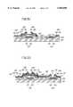
- FIG. 1A and FIG. 1Bshow cross-sectional views of the intermediate structures in the step of etching a double layer of chromium/chromium nitride according to an embodiment of the present invention.
- FIG. 2illustrates a cross-sectional view showing the etching slope of a complex layer of chromium/chromium nitride/chromium nitride according to the embodiment of the present invention.
- FIG. 3illustrates a layout showing the manufacturing process of the TFT substrate according to the embodiment of the present invention.
- FIG. 4illustrates a cross-sectional view of the TFT substrate shown in FIG. 3 along the line IV-IV'.
- FIG. 5A-5Dillustrate cross-sectional views of intermediate structures illustrating a method of manufacturing the TFT substrate shown in FIG. 4.
- a single layer of chromium, a double layer of chromium/chromium nitride, and a single layer of chromium nitrideare compared. All the layers are formed by reactive sputtering using a chromium target, and the chromium layer or the chromium nitride layer is deposited by controlling the flux of argon gas and nitrogen gas. That is, the chromium layer is formed by flowing only argon gas, and the chromium nitride layer is formed by flowing a proper mixture of argon gas and nitrogen gas.
- the fluxes of argon and nitrogen gasare shown in Table 1.
- the unit of the fluxis sccm.
- resistivityFor the layers formed by the above-mentioned method, resistivity, surface reflectivity and thickness are measured, and they are shown in Table 2.
- the resistivity of a single layer of chromium nitrideis very large, and the resistivity decreases as the ratio of nitrogen in the gas increases.
- the surface reflectivity of a single layer of chromium nitrideis much smaller than that of a single layer of chromium.
- the resistivity of the double layer of chromium/chromium nitrideis larger by 0.05-0.07 ⁇ / ⁇ than the single layer of chromium and the surface reflectivity of the double layer is smaller than the single layer of chromium.
- a layer of photoresistis patterned on each of the three layers and the photoresist was hard baked at 130° C. for 30 minutes, then wet etched using (NH 4 ) 2 Ce(NO 3 ) 6 .
- the etching rates of the layer of chromium and the layer of chromium nitridewere measured during the etching process. Afterwards, the slopes of the layer of chromium and the double layer of Cr/CrNx were observed by using a SEM. The results are shown in Table 3.
- the slopeis very gentle in the range of 35°-60°, the etching rate of the layer of chromium nitride is 5-7 times larger than that of the layer of chromium.
- the chromium nitride layer 120 of 100-300 ⁇ thicknesswhich is located between the chromium layer 110 and the layer 130 of photoresist is etched first to separate the chromium layer 110 of 1,500-3,000 ⁇ thickness and the layer 130 of photoresist, as shown in FIG. 1A.
- the layer of chromium 110is isotropically etched to form a pattern having an edge with a gentle slope, as shown in FIG. 1B.
- the etching rate of the layer of the chromium nitrideincreases as the ratio of the nitrogen in the gas increases. According to the above-mentioned condition, it is possible to make a gentle slope by increasing the flux of nitrogen gas or decreasing the flux of argon gas in time. That is, a first layer 121 of chromium nitride is formed on the layer 110 of chromium, and a second layer 122 of chromium nitride is formed on the first layer 121 of chromium nitride by flowing more nitrogen gas than when the first layer 121 of chromium nitride is formed, then the layers are etched to make a stepped slope as shown in FIG. 2.
- FIG. 4illustrates a cross-sectional view of the TFT substrate shown in FIG. 3 along the line IV-IV'.
- a gate pattern including a gate line 200, a gate electrode 210 which is a branch of the gate line 200, and a gate pad 220 formed at the end of the gate line 200is formed on a substrate 100.
- the gate electrode 210 and the gate pad 220respectively include a lower layer 211 and 221 made of aluminum alloy and an upper layer 212 and 222 made of chromium nitride, and the gate line 200 consists of the double layer of aluminum alloy and chromium nitride though it is not shown in the figures.
- the gate pad 220transfers the scanning signal to the gate line 200 from the outside.
- a gate insulating layer 300 of silicon nitrideis formed on the gate pattern 200, 210, 220, and the gate insulating layer 300 has a contact hole 720 exposing the upper layer 222 of chromium nitride of the gate pad 220.
- a layer 400 of a-Si which is an active layer of TFTis formed on the gate insulating layer 300 directly above the gate electrode 210, and a layer 510, 520 of N+ a-Si thereon is formed on left and right sides of the gate electrode 210 respectively as an ohmic contact layer.
- a data line 600is formed on the gate insulating layer 300 and perpendicular to the length of the gate line 200, and at the end of the data line 600, a data pad 630 which transfers the image signal from the outside is formed.
- a source electorde 610 which is a branch of the data line 600is formed on the layer 510 of N+ a-Si, a drain electrode 620 is formed on the layer 520 of N+ a-Si.
- a gate pad connecting member 640is formed on the gate insulating layer 300 near the gate pad 220.
- the data patternincludes the data line 600, the source/drain electrodes 610, 620, the data pad 630, and the gate pad connecting member 640 respectively consisting of the lower layers 611, 621, 631, 641 of chromium and the upper layers 612, 622, 632, 642 of chromium nitride.
- a passivation layer 700is formed on the above mentioned data pattern and the layer 400 of a-Si which is not hidden with the data pattern, and contact holes 720, 710, 730, 740 are formed to expose the upper layer 222, 622, 632, 642 of the chromium nitride of the gate pad 220, the drain electrode 620, the data pad 630 and the gate pad connecting region 640, respectively.
- a pixel electrode 800which is made of ITO(indium tin oxide) and connected to the drain electrode 620 through the contact hole 710 on the passivation layer 700 is formed.
- An ITO electrode 810 for the gate padwhich is connected to the exposed gate pad 220 and the gate pad connecting region 640 and transfer the signal from the outside to the gate line 200 and an ITO electrode 820 for the data pad which is connected to the data pad 630 and transfer the signal form the outside to the data line 600.
- FIGS. 3-4a method of fabricating the TFT substrate which is illustrated in FIGS. 3-4 will be described with reference to FIGS. 5A-5D.
- the method of fabrication according to the embodiment of the present inventionuses 5 masks.
- a layer of aluminum alloy of aluminum and neodimium (Nd) and a layer of chromium nitrideare deposited successively on a transparent insulating substrate 100, and photo etched using a first mask to form a gate pattern which is made of a double layer and includes a gate line 200, a gate electrode 210 and a gate pad 220.
- the gate electrode 210consists of a lower layer 211 of aluminum alloy and an upper layer 212 of chromium nitride
- the gate pad 220consists of a lower layer 221 of aluminum alloy and an upper layer 222 of chromium nitride, though not shown in FIG. 5A, the gate line 210 has a double layer, too.
- a gate insulating layer 300 made of silicon nitride, a layer 400 of a-Si and a layer 500 of N+ a-Siare deposited sequentially, the layer 500 of N+ a-Si and the layer 400 of a-Si are photo etched using a second mask.
- a layer of chromium and a layer of chromium nitrideare deposited successively, and the layers are wet etched using a third mask to form a data pattern which is made of a double layer and includes a data line 600, a source electrode 610, a drain electrode 620, a data pad 630 and a gate pad connecting region 640. Then, using the data pattern 600, 610, 620, 630, 640 as a mask, the exposed layer 500 of N+ a-Si is dry etched to separate into two parts using gate electrode 210 as a center, and to expose the layer 400 of a-Si between the two separated layers 510, 520 of N+ a-Si.
- a passivation layer 700is formed and photo etched with the insulating layer 300 using a fourth mask to form contact holes 710, 720, 730, 740 which expose the upper layer of chromium nitride 622, 222, 632, 642 of the drain electrode 620, the gate pad 220, the data pad 630 and the gate pad connecting region 640, respectively.
- a layer of ITOis deposited and dry etched using a fifth mask to form an ITO pattern including a pixel electrode 800 and an ITO electrode 820 for the data pad which are connected to the drain electrode 620 and the data pad 630 through the contact holes 710, 730 respectively, and an ITO electrode 810 for the gate pad which is connected to the gate pad 220 and the gate pad connecting region 640 through the contact holes 720, 740 respectively.
- the ITO patternis connected to the upper layer of chromium nitride 622, 222, 632, 642 of the drain electrode 620, the gate pad 220, the data pad 630 and the gate pad connecting region 640.
- the chromium nitride layermake the contact resistance between the lower layer of chromium and the ITO layer low as a buffer layer.
- the TFT substrate which is fabricated using the above-mentioned methodis compared to the substrate which has a data pattern formed with a single layer of chromium.
- the resultswill be described below.
- the current-voltage characteristicsare measured and the results did not show a drop.
- the contact resistance between the data pattern and the ITO electrodeis decreased greatly from 1054.30 k ⁇ to 12.82 k ⁇ , but the line resistivity of the data pattern increased a little from 2.50 k ⁇ to 2.79 k ⁇ .
- the data pattern which made of a double layer of chromium and chromium nitridehas a gentle slope, so the number of bad pixels decreases. And the performance of the LCD becomes better because of the small contact resistance in the ITO electrodes. The surface reflectivity becomes smaller, and the crosstalk decreases, and the contrast ratio increases.
Landscapes
- Physics & Mathematics (AREA)
- Nonlinear Science (AREA)
- Mathematical Physics (AREA)
- Chemical & Material Sciences (AREA)
- Crystallography & Structural Chemistry (AREA)
- General Physics & Mathematics (AREA)
- Optics & Photonics (AREA)
- Engineering & Computer Science (AREA)
- Microelectronics & Electronic Packaging (AREA)
- Thin Film Transistor (AREA)
- Liquid Crystal (AREA)
Abstract
Description
TABLE 1 ______________________________________ Cr/CrNx Cr Cr CrNx CrNx ______________________________________ Ar/N.sub.2 Ar/N.sub.2 Ar/N.sub.2 Ar/N.sub.2 50/0 50/0 50/150 50/150 50/0 140/150 140/150 ______________________________________
TABLE 2 ______________________________________ Ar/N.sub.2 resistivity surface thickness (sccm) (Ω/□) reflectivity (%) (Å) ______________________________________ Cr 50/0 1.32 170 1,500 Cr/CrNx 50/150 1.37 142 1,713 140/150 1.39 134 1,717 CrNx 50/150 1,275 71.5 753 140/150 2,004 74.4 933 ______________________________________
TABLE 3 ______________________________________ Ar/N.sub.2 (sccm) etching rate (Å/min) slope (°) ______________________________________ Cr 50/0 740 90 Cr/CrNx 50/150 -- 35-45 140/150 -- 50-60 CrNx 50/150 5,500 -- 140/150 3,609 -- ______________________________________
Claims (32)
Applications Claiming Priority (4)
| Application Number | Priority Date | Filing Date | Title |
|---|---|---|---|
| KR19960045473 | 1996-10-11 | ||
| KR96-45473 | 1996-10-11 | ||
| KR1019970024847AKR100268103B1 (en) | 1996-10-11 | 1997-06-16 | Wiring using chromium nitride and its manufacturing method, liquid crystal display device using the same, and its manufacturing method |
| KR97-24847 | 1997-06-16 |
Publications (1)
| Publication Number | Publication Date |
|---|---|
| US5968850Atrue US5968850A (en) | 1999-10-19 |
Family
ID=26632197
Family Applications (1)
| Application Number | Title | Priority Date | Filing Date |
|---|---|---|---|
| US08/947,864Expired - LifetimeUS5968850A (en) | 1996-10-11 | 1997-10-09 | Wiring using chromium nitride and methods of fabrication therefor, liquid crystal display panels using the same wiring and methods of fabrication therefor |
Country Status (2)
| Country | Link |
|---|---|
| US (1) | US5968850A (en) |
| KR (1) | KR100268103B1 (en) |
Cited By (21)
| Publication number | Priority date | Publication date | Assignee | Title |
|---|---|---|---|---|
| US6166785A (en)* | 1998-10-02 | 2000-12-26 | Lg. Philips Lcd Co., Ltd. | Thin film transistor and fabricating method thereof having patterned active layer |
| US6190934B1 (en)* | 1997-07-04 | 2001-02-20 | Lg.Philips Lcd Co., Ltd. | Liquid crystal display device and a method for manufacturing the same |
| US6261144B1 (en)* | 1997-10-03 | 2001-07-17 | Hitachi, Ltd | Wiring substrate and gas discharge display device and method therefor |
| US6410411B1 (en)* | 1996-09-21 | 2002-06-25 | Koninklijke Philips Electronics N.V. | Electronic device and their manufacture |
| US6448117B1 (en)* | 1999-12-20 | 2002-09-10 | Hannstar Display Corp. | Tri-layer process for forming TFT matrix of LCD with gate metal layer around pixel electrode as black matrix |
| US20040173567A1 (en)* | 2002-12-25 | 2004-09-09 | Tsuyoshi Katoh | Method of forming a lamination film pattern and improved lamination film pattern |
| US20040212772A1 (en)* | 2000-05-25 | 2004-10-28 | Manabu Hanakawa | Liquid crystal device, manufacturing method therefor, and electronic apparatus |
| US20050190174A1 (en)* | 1999-04-16 | 2005-09-01 | Kim Sang-Soo | Liquid crystal display panel with signal transmission patterns |
| US7102718B1 (en) | 2000-03-16 | 2006-09-05 | Semiconductor Energy Laboratory Co., Ltd. | Liquid crystal display device with particular TFT structure and method of manufacturing the same |
| US20070155180A1 (en)* | 2006-01-05 | 2007-07-05 | Chunghwa Picture Tubes, Ltd. | Thin film etching method |
| US20090033818A1 (en)* | 1999-08-12 | 2009-02-05 | Semiconductor Energy Laboratory Co., Ltd. | Semiconductor Device and Method of Manufacturing the Semiconductor Device |
| US20090073100A1 (en)* | 1999-04-16 | 2009-03-19 | Samsung Electronics Col, Ltd. | Signal transmission film and a liquid crystal display panel having the same |
| US20090236604A1 (en)* | 2008-03-20 | 2009-09-24 | Bae Ju-Han | Thin film transistor substrates and method of manufacturing the same |
| US7652294B2 (en) | 2000-03-08 | 2010-01-26 | Semiconductor Energy Laboratory Co., Ltd. | Semiconductor device and manufacturing method thereof |
| US7687325B2 (en) | 2000-03-13 | 2010-03-30 | Semiconductor Energy Laboratory Co., Ltd. | Semiconductor device and manufacturing method thereof |
| US7705354B2 (en) | 2000-03-06 | 2010-04-27 | Semiconductor Energy Laboratory Co., Ltd | Semiconductor device and method for fabricating the same |
| US7714329B2 (en) | 2001-03-06 | 2010-05-11 | Semiconductor Energy Laboratory Co., Ltd. | Semiconductor device having thin film transistor |
| US7714975B1 (en) | 2000-03-17 | 2010-05-11 | Semiconductor Energy Laboratory Co., Ltd | Liquid crystal display device and manfacturing method thereof |
| US20100294651A1 (en)* | 2007-10-12 | 2010-11-25 | Ulvac Coating Corporation | Process for producing gray tone mask |
| US7902550B2 (en) | 2000-05-09 | 2011-03-08 | Semiconductor Energy Laboratory Co., Ltd. | Semiconductor device and manufacturing method thereof |
| US8300201B2 (en) | 2000-03-13 | 2012-10-30 | Semiconductor Energy Laboratory Co., Ltd. | Semiconductor device and a method of manufacturing the same |
Families Citing this family (1)
| Publication number | Priority date | Publication date | Assignee | Title |
|---|---|---|---|---|
| KR100669451B1 (en)* | 2000-02-15 | 2007-01-15 | 삼성에스디아이 주식회사 | How to form black matrix etchant and black matrix |
Citations (3)
| Publication number | Priority date | Publication date | Assignee | Title |
|---|---|---|---|---|
| US4970368A (en)* | 1984-06-08 | 1990-11-13 | Semiconductor Energy Laboratory Co. Ltd. | Laser scribing method |
| US5234541A (en)* | 1990-06-04 | 1993-08-10 | U.S. Philips Corporation | Methods of fabricating mim type device arrays and display devices incorporating such arrays |
| US5792705A (en)* | 1996-06-28 | 1998-08-11 | Taiwan Semiconductor Manufacturing Company, Ltd. | Optimized planarization process for SOG filled vias |
Family Cites Families (2)
| Publication number | Priority date | Publication date | Assignee | Title |
|---|---|---|---|---|
| JPH08254680A (en)* | 1995-03-17 | 1996-10-01 | Toshiba Corp | Semiconductor device and manufacturing method thereof |
| KR0158538B1 (en)* | 1996-06-21 | 1998-11-16 | 한철우 | Multilayered coating material |
- 1997
- 1997-06-16KRKR1019970024847Apatent/KR100268103B1/ennot_activeExpired - Fee Related
- 1997-10-09USUS08/947,864patent/US5968850A/ennot_activeExpired - Lifetime
Patent Citations (3)
| Publication number | Priority date | Publication date | Assignee | Title |
|---|---|---|---|---|
| US4970368A (en)* | 1984-06-08 | 1990-11-13 | Semiconductor Energy Laboratory Co. Ltd. | Laser scribing method |
| US5234541A (en)* | 1990-06-04 | 1993-08-10 | U.S. Philips Corporation | Methods of fabricating mim type device arrays and display devices incorporating such arrays |
| US5792705A (en)* | 1996-06-28 | 1998-08-11 | Taiwan Semiconductor Manufacturing Company, Ltd. | Optimized planarization process for SOG filled vias |
Cited By (64)
| Publication number | Priority date | Publication date | Assignee | Title |
|---|---|---|---|---|
| US6410411B1 (en)* | 1996-09-21 | 2002-06-25 | Koninklijke Philips Electronics N.V. | Electronic device and their manufacture |
| US6190934B1 (en)* | 1997-07-04 | 2001-02-20 | Lg.Philips Lcd Co., Ltd. | Liquid crystal display device and a method for manufacturing the same |
| US6261144B1 (en)* | 1997-10-03 | 2001-07-17 | Hitachi, Ltd | Wiring substrate and gas discharge display device and method therefor |
| US6346772B1 (en) | 1997-10-03 | 2002-02-12 | Hitachi, Ltd. | Wiring substrate and gas discharge display device that includes a dry etched layer wet-etched first or second electrodes |
| US6621217B2 (en) | 1997-10-03 | 2003-09-16 | Hitachi, Ltd. | Wiring substrate and gas discharge display device |
| US6166785A (en)* | 1998-10-02 | 2000-12-26 | Lg. Philips Lcd Co., Ltd. | Thin film transistor and fabricating method thereof having patterned active layer |
| US20090073100A1 (en)* | 1999-04-16 | 2009-03-19 | Samsung Electronics Col, Ltd. | Signal transmission film and a liquid crystal display panel having the same |
| US20080062109A1 (en)* | 1999-04-16 | 2008-03-13 | Kim Sang-Soo | Liquid crystal display panel with signal transmission patterns |
| US8031150B2 (en) | 1999-04-16 | 2011-10-04 | Samsung Electronics Co., Ltd. | Liquid crystal display panel with signal transmission patterns |
| US7295196B2 (en)* | 1999-04-16 | 2007-11-13 | Samsung Electronics Co., Ltd. | Liquid crystal display panel with signal transmission patterns |
| US20050190174A1 (en)* | 1999-04-16 | 2005-09-01 | Kim Sang-Soo | Liquid crystal display panel with signal transmission patterns |
| US9640630B2 (en) | 1999-08-12 | 2017-05-02 | Semiconductor Energy Laboratory Co., Ltd. | Semiconductor device and method of manufacturing the semiconductor device |
| US9041875B2 (en) | 1999-08-12 | 2015-05-26 | Semiconductor Energy Laboratory Co., Ltd. | Semiconductor device and method of manufacturing the semiconductor device |
| US8003989B2 (en) | 1999-08-12 | 2011-08-23 | Semiconductor Energy Laboratory Co., Ltd. | Thin film semiconductor device having a terminal portion |
| US8023055B2 (en) | 1999-08-12 | 2011-09-20 | Semiconductor Energy Laboratory Co., Ltd. | Semiconductor device and method of manufacturing the semiconductor device |
| US20090061574A1 (en)* | 1999-08-12 | 2009-03-05 | Semiconductor Energy Laboratory Co., Ltd. | Semiconductor Device and Method of Manufacturing The Semiconductor Device |
| US8654270B2 (en) | 1999-08-12 | 2014-02-18 | Semiconductor Energy Laboratory Co., Ltd. | Semiconductor device and method of manufacturing the semiconductor device |
| US20090033818A1 (en)* | 1999-08-12 | 2009-02-05 | Semiconductor Energy Laboratory Co., Ltd. | Semiconductor Device and Method of Manufacturing the Semiconductor Device |
| US6448117B1 (en)* | 1999-12-20 | 2002-09-10 | Hannstar Display Corp. | Tri-layer process for forming TFT matrix of LCD with gate metal layer around pixel electrode as black matrix |
| US7973312B2 (en) | 2000-03-06 | 2011-07-05 | Semiconductor Energy Laboratory Co., Ltd. | Semiconductor device and method of fabricating the same |
| US9099355B2 (en) | 2000-03-06 | 2015-08-04 | Semiconductor Energy Laboratory Co., Ltd. | Semiconductor device and method of fabricating the same |
| US8188478B2 (en) | 2000-03-06 | 2012-05-29 | Semiconductor Energy Laboratory Co., Ltd. | Semiconductor device and method of fabricating the same |
| US7705354B2 (en) | 2000-03-06 | 2010-04-27 | Semiconductor Energy Laboratory Co., Ltd | Semiconductor device and method for fabricating the same |
| US9368514B2 (en) | 2000-03-08 | 2016-06-14 | Semiconductor Energy Laboratory Co., Ltd. | Semiconductor device and manufacturing method thereof |
| US8586988B2 (en) | 2000-03-08 | 2013-11-19 | Semiconductor Energy Laboratory Co., Ltd. | Semiconductor device and manufacturing method thereof |
| US8198630B2 (en) | 2000-03-08 | 2012-06-12 | Semiconductor Energy Laboratory Co., Ltd. | Semiconductor device and manufacturing method thereof |
| US9786687B2 (en) | 2000-03-08 | 2017-10-10 | Semiconductor Energy Laboratory Co., Ltd. | Semiconductor device and manufacturing method thereof |
| US7652294B2 (en) | 2000-03-08 | 2010-01-26 | Semiconductor Energy Laboratory Co., Ltd. | Semiconductor device and manufacturing method thereof |
| US7728334B2 (en) | 2000-03-08 | 2010-06-01 | Semiconductor Energy Laboratory Co., Ltd. | Semiconductor device and manufacturing method thereof |
| US9059045B2 (en) | 2000-03-08 | 2015-06-16 | Semiconductor Energy Laboratory Co., Ltd. | Semiconductor device and manufacturing method thereof |
| US8300201B2 (en) | 2000-03-13 | 2012-10-30 | Semiconductor Energy Laboratory Co., Ltd. | Semiconductor device and a method of manufacturing the same |
| US8934066B2 (en) | 2000-03-13 | 2015-01-13 | Semiconductor Energy Laboratory Co., Ltd. | Semiconductor device having stick drivers and a method of manufacturing the same |
| US7687325B2 (en) | 2000-03-13 | 2010-03-30 | Semiconductor Energy Laboratory Co., Ltd. | Semiconductor device and manufacturing method thereof |
| US8228477B2 (en) | 2000-03-16 | 2012-07-24 | Semiconductor Energy Laboratory Co., Ltd. | Liquid crystal display device and method of manufacturing the same |
| US8610861B2 (en) | 2000-03-16 | 2013-12-17 | Semiconductor Energy Laboratory Co., Ltd. | Liquid crystal display device and method of manufacturing the same |
| US7990508B2 (en) | 2000-03-16 | 2011-08-02 | Semiconductor Energy Laboratory Co., Ltd. | Liquid crystal display device and method of manufacturing the same |
| US7102718B1 (en) | 2000-03-16 | 2006-09-05 | Semiconductor Energy Laboratory Co., Ltd. | Liquid crystal display device with particular TFT structure and method of manufacturing the same |
| US9298056B2 (en) | 2000-03-16 | 2016-03-29 | Semiconductor Energy Laboratory Co., Ltd. | Liquid crystal display device and method of manufacturing the same |
| US8873011B2 (en) | 2000-03-16 | 2014-10-28 | Semiconductor Energy Laboratory Co., Ltd. | Liquid crystal display device and method of manufacturing the same |
| US7656491B2 (en) | 2000-03-16 | 2010-02-02 | Semiconductor Energy Laboratory Co., Ltd. | Liquid crystal display device and method of manufacturing the same |
| US8558983B2 (en) | 2000-03-17 | 2013-10-15 | Semiconductor Energy Laboratory Co., Ltd. | Liquid crystal display device and manufacturing method thereof |
| US8421985B2 (en) | 2000-03-17 | 2013-04-16 | Semiconductor Energy Laboratory Co., Ltd. | Liquid crystal display device and manufacturing method thereof |
| US7714975B1 (en) | 2000-03-17 | 2010-05-11 | Semiconductor Energy Laboratory Co., Ltd | Liquid crystal display device and manfacturing method thereof |
| US9048146B2 (en) | 2000-05-09 | 2015-06-02 | Semiconductor Energy Laboratory Co., Ltd. | Semiconductor device and manufacturing method thereof |
| US8525173B2 (en) | 2000-05-09 | 2013-09-03 | Semiconductor Energy Laboratory Co., Ltd. | Semiconductor device and manufacturing method thereof |
| US9429807B2 (en) | 2000-05-09 | 2016-08-30 | Semiconductor Energy Laboratory Co., Ltd. | Semiconductor device and manufacturing method thereof |
| US7902550B2 (en) | 2000-05-09 | 2011-03-08 | Semiconductor Energy Laboratory Co., Ltd. | Semiconductor device and manufacturing method thereof |
| US8823004B2 (en) | 2000-05-09 | 2014-09-02 | Semiconductor Energy Laboratory Co., Ltd. | Semiconductor device and manufacturing method thereof |
| US20040212772A1 (en)* | 2000-05-25 | 2004-10-28 | Manabu Hanakawa | Liquid crystal device, manufacturing method therefor, and electronic apparatus |
| US7092050B2 (en) | 2000-05-25 | 2006-08-15 | Seiko Epson Corporation | Liquid crystal device, manufacturing method therefor, and electronic apparatus |
| US8053781B2 (en) | 2001-03-06 | 2011-11-08 | Semiconductor Energy Laboratory Co., Ltd. | Semiconductor device having thin film transistor |
| US8461596B2 (en) | 2001-03-06 | 2013-06-11 | Semiconductor Energy Laboratory Co., Ltd. | Semiconductor device including semiconductor film with outer end having tapered shape |
| US7875886B2 (en) | 2001-03-06 | 2011-01-25 | Semiconductor Energy Laboratory Co., Ltd. | Semiconductor device having a thin film transistor |
| US7714329B2 (en) | 2001-03-06 | 2010-05-11 | Semiconductor Energy Laboratory Co., Ltd. | Semiconductor device having thin film transistor |
| US20060081870A1 (en)* | 2002-12-25 | 2006-04-20 | Nec Lcd Technologies, Ltd. | Method of forming a lamination film pattern and improved lamination film pattern |
| US7554207B2 (en) | 2002-12-25 | 2009-06-30 | Nec Lcd Technologies, Ltd. | Method of forming a lamination film pattern and improved lamination film pattern |
| US7012029B2 (en)* | 2002-12-25 | 2006-03-14 | Nec Lcd Technologies, Ltd. | Method of forming a lamination film pattern and improved lamination film pattern |
| US20040173567A1 (en)* | 2002-12-25 | 2004-09-09 | Tsuyoshi Katoh | Method of forming a lamination film pattern and improved lamination film pattern |
| US20070155180A1 (en)* | 2006-01-05 | 2007-07-05 | Chunghwa Picture Tubes, Ltd. | Thin film etching method |
| US20100294651A1 (en)* | 2007-10-12 | 2010-11-25 | Ulvac Coating Corporation | Process for producing gray tone mask |
| US20090236604A1 (en)* | 2008-03-20 | 2009-09-24 | Bae Ju-Han | Thin film transistor substrates and method of manufacturing the same |
| US20110129952A1 (en)* | 2008-03-20 | 2011-06-02 | Bae Ju-Han | Thin film transistor substrates and method of manufacturing the same |
| US7888717B2 (en)* | 2008-03-20 | 2011-02-15 | Samsung Electronics Co., Ltd. | Thin film transistor substrate having color filter with reverse taper shape |
| US8293564B2 (en) | 2008-03-20 | 2012-10-23 | Samsung Display Co., Ltd. | Method of manufacturing thin film transistor substrate |
Also Published As
| Publication number | Publication date |
|---|---|
| KR19980032165A (en) | 1998-07-25 |
| KR100268103B1 (en) | 2000-10-16 |
Similar Documents
| Publication | Publication Date | Title |
|---|---|---|
| US5968850A (en) | Wiring using chromium nitride and methods of fabrication therefor, liquid crystal display panels using the same wiring and methods of fabrication therefor | |
| US7943519B2 (en) | Etchant, method for fabricating interconnection line using the etchant, and method for fabricating thin film transistor substrate using the etchant | |
| US6081308A (en) | Method for manufacturing liquid crystal display | |
| US6878966B2 (en) | Thin-film transistor display devices | |
| JP4903667B2 (en) | Method for manufacturing thin film transistor substrate for display device | |
| US7470571B2 (en) | Thin film transistor array substrate and method of producing the same | |
| US7524706B2 (en) | Method of fabricating a thin film transistor array panel | |
| JP3238020B2 (en) | Method for manufacturing active matrix display device | |
| US6859252B2 (en) | Active matrix substrate and manufacturing method thereof | |
| WO2002089177A2 (en) | A contact structure of a wiring line and method manufacturing the same, and thin film transistor array substrate including the contact structure and method manufacturing the same | |
| US6757031B2 (en) | Metal contact structure and method for thin film transistor array in liquid crystal display | |
| JP2000002892A (en) | Liquid crystal display device, matrix array substrate and method of manufacturing the same | |
| US20080224093A1 (en) | Etchant for signal wire and method of manufacturing thin film transistor array panel using etchant | |
| US7599037B2 (en) | Thin film transistor array panel for liquid crystal display and method for manufacturing the same | |
| US8093595B2 (en) | Thin film array panel and manufacturing method thereof | |
| JPH0992840A (en) | Liquid crystal display device and its manufacture | |
| US6087272A (en) | Method of producing thin film transistor | |
| JPH04240824A (en) | Array substrate for liquid crystal display devices | |
| KR100471765B1 (en) | Thin film transistor substrate with single film gate line and manufacturing method | |
| JPH04155315A (en) | Manufacture of multi-layer film wiring body | |
| KR100848102B1 (en) | Thin film transistor substrate and manufacturing method thereof | |
| JPH05323378A (en) | Array substrate for liquid crystal display | |
| JP3169591B2 (en) | Active matrix circuit board and dry etching method for silicon-based insulating thin film | |
| JP2001053067A (en) | Active matrix circuit board and method of manufacturing the same | |
| KR20000025563A (en) | Method for manufacturing thin film transistor |
Legal Events
| Date | Code | Title | Description |
|---|---|---|---|
| AS | Assignment | Owner name:SAMSUNG ELECTRONICS CO., LTD., KOREA, REPUBLIC OF Free format text:ASSIGNMENT OF ASSIGNORS INTEREST;ASSIGNORS:JEONG, JONG-IN;JEONG, CHEOL-SU;PARK, DAE-WON;AND OTHERS;REEL/FRAME:009142/0191 Effective date:19980409 | |
| STCF | Information on status: patent grant | Free format text:PATENTED CASE | |
| FEPP | Fee payment procedure | Free format text:PAYOR NUMBER ASSIGNED (ORIGINAL EVENT CODE: ASPN); ENTITY STATUS OF PATENT OWNER: LARGE ENTITY | |
| FPAY | Fee payment | Year of fee payment:4 | |
| FPAY | Fee payment | Year of fee payment:8 | |
| FEPP | Fee payment procedure | Free format text:PAYER NUMBER DE-ASSIGNED (ORIGINAL EVENT CODE: RMPN); ENTITY STATUS OF PATENT OWNER: LARGE ENTITY Free format text:PAYOR NUMBER ASSIGNED (ORIGINAL EVENT CODE: ASPN); ENTITY STATUS OF PATENT OWNER: LARGE ENTITY | |
| FPAY | Fee payment | Year of fee payment:12 | |
| AS | Assignment | Owner name:SAMSUNG DISPLAY CO., LTD., KOREA, REPUBLIC OF Free format text:ASSIGNMENT OF ASSIGNORS INTEREST;ASSIGNOR:SAMSUNG ELECTRONICS CO., LTD.;REEL/FRAME:028984/0774 Effective date:20120904 |