US5966800A - Method of making a magnetic head with aligned pole tips and pole layers formed of high magnetic moment material - Google Patents
Method of making a magnetic head with aligned pole tips and pole layers formed of high magnetic moment materialDownload PDFInfo
- Publication number
- US5966800A US5966800AUS08/901,462US90146297AUS5966800AUS 5966800 AUS5966800 AUS 5966800AUS 90146297 AUS90146297 AUS 90146297AUS 5966800 AUS5966800 AUS 5966800A
- Authority
- US
- United States
- Prior art keywords
- layer
- pole tip
- magnetic head
- layers
- pole
- Prior art date
- Legal status (The legal status is an assumption and is not a legal conclusion. Google has not performed a legal analysis and makes no representation as to the accuracy of the status listed.)
- Expired - Lifetime
Links
- 230000005291magnetic effectEffects0.000titleclaimsabstractdescription119
- 239000000463materialSubstances0.000titleclaimsabstractdescription30
- 238000004519manufacturing processMethods0.000titleabstractdescription16
- 239000010410layerSubstances0.000claimsdescription180
- 238000000034methodMethods0.000claimsdescription36
- 239000000758substrateSubstances0.000claimsdescription23
- 238000000151depositionMethods0.000claimsdescription11
- 239000011241protective layerSubstances0.000claimsdescription11
- 238000004544sputter depositionMethods0.000claimsdescription11
- 230000001939inductive effectEffects0.000claimsdescription10
- 238000000992sputter etchingMethods0.000claimsdescription8
- 238000005530etchingMethods0.000claimsdescription7
- 238000000059patterningMethods0.000claimsdescription7
- 229910001257Nb alloyInorganic materials0.000claimsdescription5
- 229910001362Ta alloysInorganic materials0.000claimsdescription5
- BDVUYXNQWZQBBN-UHFFFAOYSA-N[Co].[Zr].[Nb]Chemical compound[Co].[Zr].[Nb]BDVUYXNQWZQBBN-UHFFFAOYSA-N0.000claimsdescription5
- ZGWQKLYPIPNASE-UHFFFAOYSA-N[Co].[Zr].[Ta]Chemical compound[Co].[Zr].[Ta]ZGWQKLYPIPNASE-UHFFFAOYSA-N0.000claimsdescription5
- 229910045601alloyInorganic materials0.000claimsdescription5
- 239000000956alloySubstances0.000claimsdescription5
- RNRAZTYOQURAEF-UHFFFAOYSA-Niron tantalumChemical compound[Fe].[Fe].[Fe].[Fe].[Fe].[Fe].[Fe].[Ta].[Ta].[Ta]RNRAZTYOQURAEF-UHFFFAOYSA-N0.000claimsdescription5
- 230000000873masking effectEffects0.000claimsdescription5
- 230000002463transducing effectEffects0.000claimsdescription5
- 238000010884ion-beam techniqueMethods0.000claimsdescription2
- 230000004907fluxEffects0.000abstractdescription13
- 230000008569processEffects0.000description24
- 229920002120photoresistant polymerPolymers0.000description18
- VYPSYNLAJGMNEJ-UHFFFAOYSA-NSilicium dioxideChemical compoundO=[Si]=OVYPSYNLAJGMNEJ-UHFFFAOYSA-N0.000description16
- 239000000377silicon dioxideSubstances0.000description8
- PNEYBMLMFCGWSK-UHFFFAOYSA-Naluminium oxideInorganic materials[O-2].[O-2].[O-2].[Al+3].[Al+3]PNEYBMLMFCGWSK-UHFFFAOYSA-N0.000description6
- 239000003989dielectric materialSubstances0.000description6
- 238000003860storageMethods0.000description6
- 229910018404Al2 O3Inorganic materials0.000description5
- 238000000206photolithographyMethods0.000description5
- 229910005435FeTaNInorganic materials0.000description4
- 239000010949copperSubstances0.000description4
- 239000000696magnetic materialSubstances0.000description4
- 238000000623plasma-assisted chemical vapour depositionMethods0.000description4
- 230000002028prematureEffects0.000description4
- 235000012239silicon dioxideNutrition0.000description4
- 239000010409thin filmSubstances0.000description4
- 229910052581Si3N4Inorganic materials0.000description3
- 230000015572biosynthetic processEffects0.000description3
- 230000001965increasing effectEffects0.000description3
- HQVNEWCFYHHQES-UHFFFAOYSA-Nsilicon nitrideChemical compoundN12[Si]34N5[Si]62N3[Si]51N64HQVNEWCFYHHQES-UHFFFAOYSA-N0.000description3
- 238000004804windingMethods0.000description3
- ROOXNKNUYICQNP-UHFFFAOYSA-Nammonium persulfateChemical compound[NH4+].[NH4+].[O-]S(=O)(=O)OOS([O-])(=O)=OROOXNKNUYICQNP-UHFFFAOYSA-N0.000description2
- 230000008901benefitEffects0.000description2
- 239000012777electrically insulating materialSubstances0.000description2
- 150000002500ionsChemical class0.000description2
- 229910052751metalInorganic materials0.000description2
- 239000002184metalSubstances0.000description2
- 238000003801millingMethods0.000description2
- 229910000889permalloyInorganic materials0.000description2
- 230000004044responseEffects0.000description2
- 229920006395saturated elastomerPolymers0.000description2
- 230000035945sensitivityEffects0.000description2
- 238000000926separation methodMethods0.000description2
- HBMJWWWQQXIZIP-UHFFFAOYSA-Nsilicon carbideChemical compound[Si+]#[C-]HBMJWWWQQXIZIP-UHFFFAOYSA-N0.000description2
- 239000002002slurrySubstances0.000description2
- 239000002904solventSubstances0.000description2
- MTPVUVINMAGMJL-UHFFFAOYSA-Ntrimethyl(1,1,2,2,2-pentafluoroethyl)silaneChemical compoundC[Si](C)(C)C(F)(F)C(F)(F)FMTPVUVINMAGMJL-UHFFFAOYSA-N0.000description2
- PIGFYZPCRLYGLF-UHFFFAOYSA-NAluminum nitrideChemical compound[Al]#NPIGFYZPCRLYGLF-UHFFFAOYSA-N0.000description1
- RYGMFSIKBFXOCR-UHFFFAOYSA-NCopperChemical compound[Cu]RYGMFSIKBFXOCR-UHFFFAOYSA-N0.000description1
- 229910001030Iron–nickel alloyInorganic materials0.000description1
- 229910007277Si3 N4Inorganic materials0.000description1
- 229910001870ammonium persulfateInorganic materials0.000description1
- 229910052799carbonInorganic materials0.000description1
- 229910052802copperInorganic materials0.000description1
- 230000003247decreasing effectEffects0.000description1
- 230000008021depositionEffects0.000description1
- 238000007598dipping methodMethods0.000description1
- 230000000694effectsEffects0.000description1
- 238000009713electroplatingMethods0.000description1
- 239000003302ferromagnetic materialSubstances0.000description1
- 230000017525heat dissipationEffects0.000description1
- 239000011810insulating materialSubstances0.000description1
- 238000001459lithographyMethods0.000description1
- 230000035699permeabilityEffects0.000description1
- 230000001681protective effectEffects0.000description1
- 238000001039wet etchingMethods0.000description1
Images


Classifications
- G—PHYSICS
- G11—INFORMATION STORAGE
- G11B—INFORMATION STORAGE BASED ON RELATIVE MOVEMENT BETWEEN RECORD CARRIER AND TRANSDUCER
- G11B5/00—Recording by magnetisation or demagnetisation of a record carrier; Reproducing by magnetic means; Record carriers therefor
- G11B5/127—Structure or manufacture of heads, e.g. inductive
- G11B5/31—Structure or manufacture of heads, e.g. inductive using thin films
- G11B5/3103—Structure or manufacture of integrated heads or heads mechanically assembled and electrically connected to a support or housing
- G11B5/3106—Structure or manufacture of integrated heads or heads mechanically assembled and electrically connected to a support or housing where the integrated or assembled structure comprises means for conditioning against physical detrimental influence, e.g. wear, contamination
- G—PHYSICS
- G11—INFORMATION STORAGE
- G11B—INFORMATION STORAGE BASED ON RELATIVE MOVEMENT BETWEEN RECORD CARRIER AND TRANSDUCER
- G11B5/00—Recording by magnetisation or demagnetisation of a record carrier; Reproducing by magnetic means; Record carriers therefor
- G11B5/127—Structure or manufacture of heads, e.g. inductive
- G11B5/31—Structure or manufacture of heads, e.g. inductive using thin films
- G11B5/3109—Details
- G11B5/3116—Shaping of layers, poles or gaps for improving the form of the electrical signal transduced, e.g. for shielding, contour effect, equalizing, side flux fringing, cross talk reduction between heads or between heads and information tracks
- G—PHYSICS
- G11—INFORMATION STORAGE
- G11B—INFORMATION STORAGE BASED ON RELATIVE MOVEMENT BETWEEN RECORD CARRIER AND TRANSDUCER
- G11B5/00—Recording by magnetisation or demagnetisation of a record carrier; Reproducing by magnetic means; Record carriers therefor
- G11B5/127—Structure or manufacture of heads, e.g. inductive
- G11B5/31—Structure or manufacture of heads, e.g. inductive using thin films
- G11B5/3109—Details
- G11B5/313—Disposition of layers
- G11B5/3143—Disposition of layers including additional layers for improving the electromagnetic transducing properties of the basic structure, e.g. for flux coupling, guiding or shielding
- G11B5/3146—Disposition of layers including additional layers for improving the electromagnetic transducing properties of the basic structure, e.g. for flux coupling, guiding or shielding magnetic layers
- G11B5/3153—Disposition of layers including additional layers for improving the electromagnetic transducing properties of the basic structure, e.g. for flux coupling, guiding or shielding magnetic layers including at least one magnetic thin film coupled by interfacing to the basic magnetic thin film structure
- G—PHYSICS
- G11—INFORMATION STORAGE
- G11B—INFORMATION STORAGE BASED ON RELATIVE MOVEMENT BETWEEN RECORD CARRIER AND TRANSDUCER
- G11B5/00—Recording by magnetisation or demagnetisation of a record carrier; Reproducing by magnetic means; Record carriers therefor
- G11B5/127—Structure or manufacture of heads, e.g. inductive
- G11B5/31—Structure or manufacture of heads, e.g. inductive using thin films
- G11B5/3163—Fabrication methods or processes specially adapted for a particular head structure, e.g. using base layers for electroplating, using functional layers for masking, using energy or particle beams for shaping the structure or modifying the properties of the basic layers
- Y—GENERAL TAGGING OF NEW TECHNOLOGICAL DEVELOPMENTS; GENERAL TAGGING OF CROSS-SECTIONAL TECHNOLOGIES SPANNING OVER SEVERAL SECTIONS OF THE IPC; TECHNICAL SUBJECTS COVERED BY FORMER USPC CROSS-REFERENCE ART COLLECTIONS [XRACs] AND DIGESTS
- Y10—TECHNICAL SUBJECTS COVERED BY FORMER USPC
- Y10T—TECHNICAL SUBJECTS COVERED BY FORMER US CLASSIFICATION
- Y10T29/00—Metal working
- Y10T29/49—Method of mechanical manufacture
- Y10T29/49002—Electrical device making
- Y10T29/4902—Electromagnet, transformer or inductor
- Y10T29/49021—Magnetic recording reproducing transducer [e.g., tape head, core, etc.]
- Y10T29/49032—Fabricating head structure or component thereof
- Y10T29/49036—Fabricating head structure or component thereof including measuring or testing
- Y10T29/49043—Depositing magnetic layer or coating
- Y10T29/49046—Depositing magnetic layer or coating with etching or machining of magnetic material
- Y—GENERAL TAGGING OF NEW TECHNOLOGICAL DEVELOPMENTS; GENERAL TAGGING OF CROSS-SECTIONAL TECHNOLOGIES SPANNING OVER SEVERAL SECTIONS OF THE IPC; TECHNICAL SUBJECTS COVERED BY FORMER USPC CROSS-REFERENCE ART COLLECTIONS [XRACs] AND DIGESTS
- Y10—TECHNICAL SUBJECTS COVERED BY FORMER USPC
- Y10T—TECHNICAL SUBJECTS COVERED BY FORMER US CLASSIFICATION
- Y10T29/00—Metal working
- Y10T29/49—Method of mechanical manufacture
- Y10T29/49002—Electrical device making
- Y10T29/4902—Electromagnet, transformer or inductor
- Y10T29/49021—Magnetic recording reproducing transducer [e.g., tape head, core, etc.]
- Y10T29/49032—Fabricating head structure or component thereof
- Y10T29/49048—Machining magnetic material [e.g., grinding, etching, polishing]
- Y10T29/49052—Machining magnetic material [e.g., grinding, etching, polishing] by etching
Definitions
- This inventionrelates to the method of making magnetic heads having narrow pole widths with high saturation threshold levels capable of writing on magnetic media with high areal densities and coercivity.
- a typical inductive thin film magnetic headcomprises a first magnetic pole layer and a second magnetic pole layer with an electrical coil between the two pole layers.
- the two pole layerscontact each other at one end at a back closure to form a continuous magnetic path, with a narrow transducing gap at the other end.
- the portions of the first and second poles separated by the transducing gapare designated respectively as the first and second pole tips.
- the magnetic head described aboveis called an inductive head.
- the inductive headcan be combined with a data reading transducer to form a merged head.
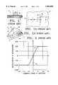
- FIG. 1shows a prior art approach in which a magnetic head 2 is fabricated with a first pole tip 4 wider in lateral dimension than a second pole tip 6.
- the wider first pole tip 4tolerates a certain degree of misalignment during the deposition of the second pole tip 6.
- the width TW of the second pole tip 6is intended to define the track width of the magnetic head 2.
- the fringing fluxsuch as flux lines F emanating from the second pole 6 to the first pole 4 as shown in FIG. 1A, would result in registering a data track 8 with a width W having ambiguous track boundaries, which seriously limit the track-to-track separations on the recording medium 10.
- Magnetic headsare fabricated on microscopically confined areas. To increase the sensitivity of the magnetic head, the number of coil windings can be increased. However, any increase in coil windings is restricted by the confined areas. Furthermore, the higher the number of coil windings, the higher is the resultant inductance attached to the magnetic head. A magnetic head with high inductance is sluggish in response to data writing current and incapable of operating at high frequency ranges.
- Another approach to increase the writing sensitivity of the magnetic headis to increase the magnitude of the writing current.
- Higher writing currentgenerates higher Joule heat which increases the burden of the magnetic heat formed in a confined space in respect to the heat dissipation.
- an overriding issueis the premature magnetic saturation encountered by the magnetic yokes in response to higher writing current.
- FIG. 2shows the hysteresis curve 12 of a magnetic material such as Permalloy (NiFe) which includes a high permeability slope of the curve 12 and low coercivity H c . Because of these characteristics, Permalloy is commonly used as the material for the magnetic yokes or tips of magnetic head.
- FIG. 2Ais a fragmentary view of the conventional magnetic head 2 at the tip portion.
- the magnetic yoke layersare fully saturated at 200 nanowebers and can no longer be responsive to any increase in writing current.
- magnetic saturationhappens at the areas with the smallest physical dimensions. For instance, when magnetic saturation occurs, it first takes place at the first and second tip layers 4 and 6 and then slowly progresses to the areas with larger physical bulk, such as the yoke bodies 16 and 18. With pole tips built smaller for the purpose of writing narrow data tracks, the problem of magnetic saturation is further exacerbated.
- a thin film magnetic headincludes first and second pole tips separated by a nonmagnetic gap layer.
- the pole tipsare made of a high magnetic moment material.
- the right side and left side walls of the first and second pole tipsare vertically aligned with each other respectively.
- the side fringing flux of one pole tip to anotheris substantially reduced resulting in a magnetic head capable of writing data tracks with well defined boundaries.
- the possibility of the pole tips running into magnetic saturationis reduced because the pole tips, made of high magnetic moment material, are tolerant of high coercivity media.
- the magnetic head of the inventioncan be fabricated as an inverted or a noninverted head.
- the aligned pole tipsare first made by depositing a tri-layer sandwich having a gap layer between the first pole layer and the second pole layer on the substrate.
- the tri-layer sandwichis then etched away through a masking layer, thereby leaving at least a stack of layers formed on the substrate.
- the stack of layersconstitutes the magnetic pole tip region of the magnetic head with aligned sidewalls for the pole tips.
- the pole tipscan be narrowly defined, thereby allowing the inventive head to write on magnetic media with narrow data track widths. The problem of premature magnetic saturation is avoided because the pole tips are made of high magnetic moment material.
- FIG. 1, as described above,is a cross-sectional front view of a prior art magnetic head having the first pole tip wider in lateral dimension than the second pole tip which is characterized by misalignment of the second pole tip during fabrication;
- FIG. 1Aschematically illustrates the effect of the side fringing flux on a registered data track written by the conventional magnetic head as shown in FIG. 1;
- FIG. 2is an hystersis characteristic of a ferromagnetic material used in a conventional magnetic head
- FIG. 2Ais a fragmentary view of the magnetic head shown in FIG. 1 illustrating the tendency of the magnetic head of running into magnetic saturation starting from the pole tip region;
- FIG. 3is a top plan view, partly broken away, of an embodiment of the invention fabricated as a non-inverted head;
- FIG. 4is a cross-sectional front view taken along the line 4--4 of FIG. 3;
- FIG. 5is a cross-sectional side view taken along the line 5--5 of FIG. 3;
- FIGS. 6A-6Sare sequential views schematically illustrating the process of forming the magnetic head of the invention as shown in FIGS. 3-5;
- FIG. 7is a cross-sectional front view, shown in part, of another embodiment of the invention fabricated as an inverted head;
- FIG. 8is a cross-sectional front view taken along the line 8--8 of FIG. 7;
- FIGS. 9A-9Nare sequential views schematically illustrating the process of forming the magnetic head of the invention as shown in FIGS. 7-8.
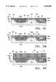
- FIG. 3shows the top plan view of a magnetic head 20, made in accordance with this invention.
- the top protective and insulating layers in FIG. 3are not illustrated so as to expose the relevant components of the magnetic head 20.
- the top layersare shown in FIGS. 4 and 5 which are cross-sectional front and side views taken along the lines 4--4 and 5--5, respectively, of FIG. 3.
- the magnetic head 20includes a first yoke layer 22 formed with a first pole tip layer 26 and disposed on a substrate 24.
- the substrate 24can be made of a non-magnetic and electrically insulating material, such as alumina titanium carbide (Al 2 O 3 TiC) or silicon carbide (SiC).
- the substrate 24can be pre-fabricated with components. For example, in a merged head, various component layers, such as a first shield layer 38 and a read transducer 39, may be fabricated in advance and thereafter serve as a substrate for the first yoke layer 22.
- a second pole layer 28Above the first yoke layer 22 is a second pole layer 28 which is formed with a second pole tip layer 30.
- inductive coils 32A and 32BSandwiched between the first and second yoke layers 22 and 28 are inductive coils 32A and 32B separated from each other by dielectric material 34 (FIG. 5).
- the coils 32A and 32Bare electrically connected to each other by means of an electrical feedthrough 36. Electrical current can be directed to and from the serially connected coils 32A and 32B via a pair of electrical leads 38A and 38B (FIG. 3).
- the first and second yoke layers 22 and 28are in direct contact at the back closure region 40 but are separated by a transducing gap layer 42 at the pole tip layers 26 and 30.
- the magnetic head 20flies above the surface of a recording medium 46 through a thin film of air. Electrical current representative of data signals passes through the inductive coils 32A and 32B via the leads 38A and 38B and induces magnetic flux. The magnetic flux at the gap 42 registers on the magnetic material coated on the medium 46.
- magnetic flux emanating from a recording medium surface 46is sensed at the gap layer 42.
- the magnetic fluxinduces electrical current in the inductive coils 32A and 32B, which represents the recorded data.
- the induced current in the coils 32A and 32Bflows through the leads 38A and 38B for further processing.
- the magnetic head 20 of the inventioncomprises vertically aligned side walls for the first and second pole tip layers 26 and 30 as shown in FIGS. 4 and 5. Specifically, the left side wall 26A of the first pole tip 26 is in vertical alignment with the left side wall 30A of the second pole tip 30. Similarly, the right side wall 26B of the first pole tip 26 is flush with the right side wall 30B of the second pole tip 30.
- the aligned side walls 26A, 30A, and 26B, 30Bsubstantially reduce fringing flux from one pole to another, thereby enabling the magnetic head 20 to write data with well defined data tracks on the medium surface 46.
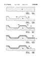
- FIGS. 6A-6Mare sequential drawings schematically illustrating the fabrication process of the magnetic head 20 of the invention.
- First a substrate 24is provided as shown in FIG. 6A.
- the substrate 24can be with or without prefabricated components.
- a first yoke layer 22is then deposited on the top of the substrate 24 by sputtering to a thickness of approximately 0.5 ⁇ -3.5 ⁇ , for example.
- the resultant structureis shown in FIG. 6B.
- a first pole tip layer 26is deposited on the first yoke layer 22 either by sputtering or electroplating to a thickness of approximately 0.8 ⁇ -2.5 ⁇ .
- Materials for the first yoke layer 22 and the first pole tip layer 26are preferably materials having a high magnetic moment, such as cobalt zirconium tantalum alloy (CoZrTa), cobalt zirconium niobium alloy (CoZrNb), and iron tantalum nitride alloy (FeTaN).
- a photoresist layer 48is then patterned on the first pole tip layer 22 by conventional photolithography. Thereafter, a gap layer 42 is deposited by sputtering as shown in FIG. 6D. The photoresist layer 48 is then removed using a photoresist solvent. The gap layer 42 deposited on the photoresist layer 48 is lifted off along with the removed photoresist material. The resultant structure up to this step is shown in FIG. 6E.
- a second pole tip layer 30is deposited on the structure by sputtering to a thickness of approximately 0.8 ⁇ -2.5 ⁇ , for example, as shown in FIG. 6F.
- Another mask 50is patterned on the second pole tip layer 30, as shown in FIG. 6G.
- the material for the mask 50can be photoresist or metal.
- the masked structureis then subject to an ion milling process.
- the mask layer 50is resistant to milling ions.
- areas not protected by the mask layer 50are removed, resulting in two stacks of layers 52 and 54 formed on the substrate 24 as shown in FIG. 6H.
- the first pole tip layer 26is separated from the second pole tip layer 30 by the gap layer 42 in the stack 52 at the pole tip region 44. However, the first pole tip layer 26 contacts the second pole tip layer 30 in the stack 54 at the back gap region 40.
- a protective layer 56is deposited on the structure with the stacks of layers 52 and 54.
- the sputtering methodis used and the protective layer 56 is deposited over and around the stacks of layers 52 and 54 to a thickness of approximately 3 ⁇ to 4 ⁇ .
- the resultant structure up to this stepis shown in FIG. 6I.
- the structureis then subject to a two-step leveling process in which the protective layer 56 is planarized via mechanical lapping with the assistance of a slurry which may include alumina (Al 2 O 3 ) or silicon dioxide (SiO 2 ) for gross material removal, for example. Thereafter, ion milling is employed for the removal of material to a fine level, thereby exposing the second pole tip layer 30.
- a slurrywhich may include alumina (Al 2 O 3 ) or silicon dioxide (SiO 2 ) for gross material removal, for example.
- ion millingis employed for the removal of material to a fine level, thereby exposing the second pole tip layer 30.
- a thin layer of copper (Cu)(not shown), called the seed layer, is then sputtered on the polished surface of the structure.
- a photoresist mask 58is then patterned on the structure as shown in FIG. 6K.
- a first coil layer 32Ais then electroplated on the patterned photoresist layer 58 as shown in FIG. 6L.
- the photoresist layer 58is thereafter removed, resulting in the formation of the first coil layer 32A disposed on the structure, which up to this step is shown in FIG. 6M.
- the Cu seed layeris then etched away by lightly dipping the substrate with the Cu seed layer in an etchant bath filled with ammonium persulfate (NH 4 ) 2 S 2 O 8 ).
- a layer of dielectric material 60is then deposited on the first coil layer 32A by either the PECVD or the sputtering method.
- the dielectric material 60can be selected from a variety of insulating materials, such as alumina (Al 2 O 3 ), silicon dioxide (SiO 2 ), silicon nitride (Si 3 N 4 ), aluminum nitride (AlN) or diamond-like-carbon (DLC).
- a feedthrough 62is then formed in the dielectric layer 60 by conventional photolithography and etching methods, as shown in FIG. 6N. The formation of the feedthrough 62 is for the purpose of electrically connecting the first coil layer 32A with the subsequently deposited second coil layer 32B.
- the process of forming second coil layer 32Bis substantially the same as forming the first coil layer 32A. For the sake of conciseness, the process of making the second coil 32B is not repeated.
- the resultant structure up to this stepis shown in FIG. 60.
- a photoresist mask 64is patterned on the dielectric material 66 as shown in FIG. 6P. Either the technique of wet etching or reactive ion beam etching (RIBE) can be employed to define the apex angles ⁇ and ⁇ of the second yoke layer 28 as shown in FIG. 6Q.
- the photoresist layer 64is then removed.
- a layer of high magnetic moment materialsuch as cobalt zirconium tantalum alloy (CoZrTa), cobalt zirconium niobium alloy (CoZrNb), or iron tantalum nitride alloy (FeTaN) is then sputtered on the structure as shown in FIG.
- the second yoke layer 28can be patterned via the conventional photolithography process, for example. Shown in FIG. 3 is the plan view of the second yoke layer 28 after the patterning process. After depositing an overcoat layer 68 on the patterned second yoke layer 28, the resultant structure is as shown in FIG. 6S.
- a final lapping stepis performed on the tip portion 44 of the magnetic head 20 for the purpose of securing a smooth air bearing surface (ABS) 70 as shown in FIG. 5.
- ABSair bearing surface
- FIGS. 7 and 8show a second embodiment of the invention fabricated as an inverted head 72.
- the magnetic head 72 of this embodimentincludes a second yoke layer 74 disposed on a substrate 76.
- the second yoke layer 74is associated with a second pole tip layer 78.
- the substrate 76can be made of a non-magnetic and electrically insulating material such as alumina titanium carbide (Al 2 O 3 TiC) or silicon carbide (SiC).
- alumina titanium carbideAl 2 O 3 TiC
- SiCsilicon carbide
- Above the second yoke layer 74is a first yoke layer 80 associated with a first pole tip layer 82.
- inductive coil layers 84A and 84Bsandwiched between the second and first yoke layers 74 and 80 are inductive coil layers 84A and 84B separated from each other by dielectric material 86.
- the coil layers 84A and 84Bare electrically connected by means of an electrical feedthrough 88.
- the second and first yoke layers 74 and 80are in direct contact at a back closure region 40.
- the first and second pole tip layers 78 and 82are separated by a gap layer 90.
- the magnetic head 72also comprises vertically aligned side walls for the second and first pole tip layers 78 and 82 as shown in FIG. 8. Specifically, the left side wall 82A of the first pole tip 82 is in vertical alignment with the left side wall 78A of the second pole tip 78. Similarly, the right side wall 82B of the first pole tip 82 is flush with the right side wall 78B of the second pole tip 78.
- FIGS. 9A-9Mare sequential drawings schematically illustrating the fabrication process of the magnetic head 72.
- the fabrication processstarts with a substrate 76 as shown in FIG. 9A. Cavities 92 are formed in the substrate 76 by the conventional process of ion milling as shown in FIG. 9B.
- a second yoke layer 74is deposited on the substrate 92 lining the cavities 92 via the process of sputtering for example, to a thickness of approximately 0.5 ⁇ -3.5 ⁇ as shown in FIG. 9C.
- a second pole tip layer 78is then electroplated or sputtered on the second yoke layer 74 as shown in FIG. 9D.
- Second yoke and pole tip layers 74 and 78Conventional photolithography and etching methods are employed to pattern the second yoke and pole tip layers 74 and 78.
- Materials for the second yoke layer 74 and the second pole tip layer 78are preferably materials having a high magnetic moment, such as cobalt zirconium tantalum alloy (CoZrTa), cobalt zirconium niobium alloy (CoZrNb), or iron tantalum nitride alloy (FeTaN).
- CoZrTacobalt zirconium tantalum alloy
- CoZrNbcobalt zirconium niobium alloy
- FeTaNiron tantalum nitride alloy
- first and second coil layers 84A and 84Babove the second pole tip layer 78 and in the cavities 92.
- the process of forming the coil layers 84A and 84Bis substantially the same as the corresponding process for the previous embodiment. For the sake of conciseness, the process is not repeated.
- the resultant structure with the deposited coil layers 84A and 84Bis shown in FIG. 9F.
- a photoresist layer 94is then patterned on the top of the structure by conventional photolithography. Thereafter, a write gap layer 90 is deposited on the masked substrate as shown in FIG. 9G. The photoresist layer 94 is then removed using a photoresist solvent. The write gap layer 94 deposited on the photoresist layer 94 is then lifted off along with the removed photoresist material. A first pole tip layer 82 is then sputtered on the top of the write gap layer 90 and the second pole tip layer 78. The resultant structure up to this step is shown in FIG. 9H.
- Another mask 96is patterned on the first pole tip layer 82.
- the material for the mask 96can be either photoresist or metal.
- the masked structureis then subject to ion milling.
- the mask layer 96is resistant to the milling ions as shown in FIG. 9I.
- areas not protected by the mask layer 96are removed, resulting in two stacks of layers 98 and 100 formed on the substrate 24 as shown in FIG. 9J.
- the second pole tip layer 78is separated from the first pole tip layer 82 by the gap layer 90 in the stack 98 at the pole tip region 44. However, the second pole tip layer 78 is in contact with the first pole tip layer 82 in the stack 100 at the back gap region 40.
- a protective layer 56is deposited on the structure with the stacks of layers 98 and 100.
- the protective layer 56is deposited over and around the stacks of layers 98 and 100 to a thickness of approximately 3 ⁇ to 4 ⁇ as shown in FIG. 9K.
- the structureis then subject to a two-step leveling process in which the protective layer 56 is planarized via mechanical lapping with the assistance of a slurry which may include alumina (Al 2 O 3 ) or silicon dioxide (SiO 3 ) for gross material removal, for example. Thereafter, the ion milling process is employed for the removal of material to a fine level, thereby exposing the second pole tip layer 82.
- a slurrywhich may include alumina (Al 2 O 3 ) or silicon dioxide (SiO 3 ) for gross material removal, for example.
- the ion milling processis employed for the removal of material to a fine level, thereby exposing the second pole tip layer 82.
- FIG. 9LThe resultant structure up to this step is shown in FIG. 9L.
- the first yoke layer 80is then deposited on the structure by the sputtering method.
- the first yoke layer 80is deposited in contact with the pole tip layer 82 at the pole tip region 44 and the back gap region 40.
- the material for the first yoke and pole tip layers 80 and 82are preferably a material with a high magnetic moment, such as cobalt zirconium tantalum alloy (CoZrTa), cobalt zirconium niobium alloy (CoZrNb), or iron tantalum nitride alloy (FeTaN).
- CoZrTacobalt zirconium tantalum alloy
- CoZrNbcobalt zirconium niobium alloy
- FeTaNiron tantalum nitride alloy
- the first yoke layer 80also acts as a second shield layer. Furthermore, a read transducer 102 and a first shield layer 104 are fabricated on the first yoke layer 80. Fabrication processes for the read transducer 102 and the first shield layer 104 are conventional and need not be further elaborated.
- the resultant structure 72 fabricated as a merged headis shown in FIG. 9N.
- the advantage of making a merged magnetic head as an inverted headis substantial.
- depositing layers for the write transducer portionsuch as the coil layers 84A and 84B and the filling dielectric layer 86 very often involve high-temperature processing cycles.
- depositing layers for the read transducer 102requires depositing and patterning of ultra-thin delicate layers which may be detrimentally affected by the higher temperature processes. Reserving the fabrication of the read transducer 102 at the end of the production process provides the benefits of preventing the read transducer from being subjected to high temperature cycles thereby improving final production yield and reliability of the magnetic head 72.
- the pole tipsare narrowly defined with aligned sidewalls, thereby enabling the magnetic head of the invention to write on magnetic media with high areal densities. Notwithstanding the narrow pole tips, the magnetic heads of the invention are less prone to run into premature magnetic saturation because the pole tips are made of high magnetic moment material, thereby allowing the magnetic heads of the invention to write on magnetic media with high coercivity and at high data rate transfer.
- the dielectric material 66 or 86need not be alumina as described.
- Other materialssuch as silicon dioxide (SiO 2 ) or silicon nitride (SiN), or hard-baked photoresist can well be used as substitutes.
Landscapes
- Engineering & Computer Science (AREA)
- Manufacturing & Machinery (AREA)
- Physics & Mathematics (AREA)
- Electromagnetism (AREA)
- Magnetic Heads (AREA)
Abstract
Description
Claims (6)
Priority Applications (4)
| Application Number | Priority Date | Filing Date | Title |
|---|---|---|---|
| US08/901,462US5966800A (en) | 1997-07-28 | 1997-07-28 | Method of making a magnetic head with aligned pole tips and pole layers formed of high magnetic moment material |
| JP10226556AJPH11110718A (en) | 1997-07-28 | 1998-07-28 | Magnetic head and its manufacture |
| US09/332,973US6118629A (en) | 1997-07-28 | 1999-06-15 | Magnetic head with aligned pole tips and pole layers formed of high magnetic moment material |
| US09/590,898US6775902B1 (en) | 1997-07-28 | 2000-06-09 | Method of making a magnetic head with aligned pole tips |
Applications Claiming Priority (1)
| Application Number | Priority Date | Filing Date | Title |
|---|---|---|---|
| US08/901,462US5966800A (en) | 1997-07-28 | 1997-07-28 | Method of making a magnetic head with aligned pole tips and pole layers formed of high magnetic moment material |
Related Child Applications (1)
| Application Number | Title | Priority Date | Filing Date |
|---|---|---|---|
| US09/332,973DivisionUS6118629A (en) | 1997-07-28 | 1999-06-15 | Magnetic head with aligned pole tips and pole layers formed of high magnetic moment material |
Publications (1)
| Publication Number | Publication Date |
|---|---|
| US5966800Atrue US5966800A (en) | 1999-10-19 |
Family
ID=25414234
Family Applications (2)
| Application Number | Title | Priority Date | Filing Date |
|---|---|---|---|
| US08/901,462Expired - LifetimeUS5966800A (en) | 1997-07-28 | 1997-07-28 | Method of making a magnetic head with aligned pole tips and pole layers formed of high magnetic moment material |
| US09/332,973Expired - LifetimeUS6118629A (en) | 1997-07-28 | 1999-06-15 | Magnetic head with aligned pole tips and pole layers formed of high magnetic moment material |
Family Applications After (1)
| Application Number | Title | Priority Date | Filing Date |
|---|---|---|---|
| US09/332,973Expired - LifetimeUS6118629A (en) | 1997-07-28 | 1999-06-15 | Magnetic head with aligned pole tips and pole layers formed of high magnetic moment material |
Country Status (2)
| Country | Link |
|---|---|
| US (2) | US5966800A (en) |
| JP (1) | JPH11110718A (en) |
Cited By (33)
| Publication number | Priority date | Publication date | Assignee | Title |
|---|---|---|---|---|
| US6158108A (en)* | 1997-06-12 | 2000-12-12 | International Business Machines Corporation | Method of making magnetic head with vialess lead layers from MR sensor to pads |
| US6195872B1 (en)* | 1998-03-12 | 2001-03-06 | Tdk Corporation | Method of manufacturing a thin film magnetic head |
| US6301084B1 (en)* | 1999-05-21 | 2001-10-09 | International Business Machines Corporation | Protection of second pole tip during fabrication of write head |
| US6329211B1 (en)* | 1998-09-29 | 2001-12-11 | Tdk Corporation | Method of manufacturing thin film magnetic head |
| US20020057526A1 (en)* | 2000-10-13 | 2002-05-16 | Tdk Corporation | Thin film magnetic head and method of manufacturing the same |
| US6417990B1 (en) | 1999-12-06 | 2002-07-09 | Seagate Technology Llc | Composite core structure for high efficiency writer |
| US6430806B1 (en) | 2000-06-23 | 2002-08-13 | Read-Rite Corporation | Method for manufacturing an inductive write element employing bi-layer photoresist to define a thin high moment pole pedestal |
| US6445536B1 (en)* | 1998-08-27 | 2002-09-03 | Read-Rite Corporation | Dielectric stencil-defined write head for MR, GMR, and spin valve high density recording heads |
| US6477005B1 (en)* | 1999-04-06 | 2002-11-05 | Tdk Corporation | Thin-film magnetic head having a magnetic layer including an auxiliary layer made of a high saturation flux density material and method of manufacturing same |
| US6519834B1 (en)* | 1999-07-14 | 2003-02-18 | Tdk Corporation | Method of manufacturing thin-film magnetic head |
| US20030066680A1 (en)* | 2001-10-04 | 2003-04-10 | Alps Electric Co., Ltd. | Terminal electrode of thin-film device with improved mounting strength, manufacturing method for the same, and thin-film magnetic head |
| US6562487B1 (en) | 2000-07-28 | 2003-05-13 | Seagate Technology Llc | Writer pole employing a high saturation moment, low permeability layer adjacent to writer gap |
| US6578252B2 (en)* | 2000-01-07 | 2003-06-17 | Tdk Corporation | Method of manufacturing a thin film magnetic head |
| US6588091B1 (en)* | 1998-08-21 | 2003-07-08 | International Business Machines Corporation | Method of making magnetic head with precisely defined zero throat height |
| US20030137767A1 (en)* | 2002-01-18 | 2003-07-24 | International Business Machines Corporation | High-saturation thin-film write head for high-coercivity magnetic data storage media |
| US6631549B1 (en)* | 1998-12-04 | 2003-10-14 | Hitachi Global Storage Technologies Netherlands B.V. | Method of making a seed layer for a nickel oxide pinning layer for increasing the magnetoresistance of a spin valve sensor |
| US6631546B1 (en)* | 2000-02-01 | 2003-10-14 | International Business Machines Corporation | Self-aligned void filling for mushroomed plating |
| US6647612B1 (en)* | 1999-02-11 | 2003-11-18 | Seagate Technology Llc | Method for constructing an ultra-low-flying-height slider |
| US6651312B1 (en)* | 1997-12-26 | 2003-11-25 | Tdk Corporation | Method for manufacturing a composite type thin film magnetic head having normal structure |
| US6668442B2 (en)* | 1998-08-28 | 2003-12-30 | Tdk Corporation | Method of manufacturing a thin film magnetic head |
| US6676813B1 (en) | 2001-03-19 | 2004-01-13 | The Regents Of The University Of California | Technology for fabrication of a micromagnet on a tip of a MFM/MRFM probe |
| US6754947B2 (en) | 1998-03-20 | 2004-06-29 | Seagate Technology Llc | Method for forming a narrow track inductive write head having two-piece pole |
| US6778357B2 (en) | 2000-11-10 | 2004-08-17 | Seagate Technology Llc | Electrodeposited high-magnetic-moment material at writer gap pole |
| US6791796B2 (en) | 2002-05-28 | 2004-09-14 | Seagate Technology Llc | Perpendicular writer with laminated main pole |
| US20040264046A1 (en)* | 2003-06-25 | 2004-12-30 | Hitachi Global Storage Technologies | Magnetic head with thinned T-shaped write pole and its fabrication |
| US6862798B2 (en) | 2002-01-18 | 2005-03-08 | Hitachi Global Storage Technologies Netherlands B.V. | Method of making a narrow pole tip by ion beam deposition |
| US20050068665A1 (en)* | 2003-09-26 | 2005-03-31 | Hitachi Global Storage Technologies | Write pole fabrication for perpendicular recording |
| US6884730B2 (en)* | 2002-07-02 | 2005-04-26 | Headway Technologies, Inc. | Method of etching a film of magnetic material and method of manufacturing a thin-film magnetic head |
| US6894870B2 (en) | 2000-11-08 | 2005-05-17 | Alps Electric Co., Ltd. | Thin film magnetic head comprising at least two coil layers and method of manufacturing the same |
| US20070097546A1 (en)* | 2005-10-28 | 2007-05-03 | Seagate Technology Llc | Laminated return pole for suppressing side track erasure |
| US20080144215A1 (en)* | 2006-12-15 | 2008-06-19 | Hitachi Global Storage Technologies | Electrical lapping guide for flare point control and trailing shield throat height in a perpendicular magnetic write head |
| US7573677B2 (en)* | 2002-03-01 | 2009-08-11 | International Business Machines Corporation | Reduction of interference pickup in heads for magnetic recording by minimizing parasitic capacitance |
| US7688545B1 (en) | 2002-09-11 | 2010-03-30 | Seagate Technology Llc | Recording head writer with high magnetic moment material at the writer gap and associated process |
Families Citing this family (147)
| Publication number | Priority date | Publication date | Assignee | Title |
|---|---|---|---|---|
| JPH11353616A (en)* | 1998-06-11 | 1999-12-24 | Tdk Corp | Thin-film magnetic head and its production |
| JP2000099916A (en)* | 1998-09-28 | 2000-04-07 | Fujitsu Ltd | Thin film magnetic head and method of manufacturing the same |
| JP3781399B2 (en)* | 1998-12-08 | 2006-05-31 | Tdk株式会社 | Thin film magnetic head and manufacturing method thereof |
| JP3455155B2 (en)* | 1999-06-28 | 2003-10-14 | アルプス電気株式会社 | Thin film magnetic head and method of manufacturing the same |
| JP2001028107A (en)* | 1999-07-14 | 2001-01-30 | Tdk Corp | Thin film magnetic head, magnetic head device, magnetic disk device and manufacture of thin film magnetic head |
| JP3492953B2 (en)* | 1999-10-05 | 2004-02-03 | Tdk株式会社 | Method for manufacturing thin-film magnetic head |
| WO2001027915A1 (en)* | 1999-10-07 | 2001-04-19 | Fujitsu Limited | Thin film magnetic head and magnetic recording medium drive device |
| US6306311B1 (en)* | 1999-11-01 | 2001-10-23 | Headway Technologies, Inc. | Method to make a high data rate stitched writer for a giant magneto-resistive head |
| US7002776B2 (en) | 1999-12-06 | 2006-02-21 | Tdk Corporation | Thin film magnetic head and method of manufacturing same |
| JP3499490B2 (en)* | 2000-02-16 | 2004-02-23 | Tdk株式会社 | Method for manufacturing thin-film magnetic head |
| US6563669B1 (en)* | 2000-09-13 | 2003-05-13 | Storage Technology Corporation | Inverted write head with high-precision track width definition |
| JP4047115B2 (en)* | 2002-09-13 | 2008-02-13 | アルプス電気株式会社 | Soft magnetic film, thin film magnetic head using the soft magnetic film, and method for manufacturing the soft magnetic film |
| US6851178B2 (en)* | 2002-10-24 | 2005-02-08 | Headway Technologies, Inc. | Process of manufacturing a magnetic write head |
| US20040112868A1 (en)* | 2002-12-13 | 2004-06-17 | Phipps Peter Beverley Powell | Etchant solution for removing a thin metallic layer |
| US6989964B2 (en) | 2003-06-16 | 2006-01-24 | Hitachi Global Storage Technologies Netherlands B.V. | Magnetic head having a pole piece with a double pedestal structure |
| US7310204B1 (en) | 2003-12-19 | 2007-12-18 | Western Digital (Fremont), Llc | Inductive writer design for using a soft magnetic pedestal having a high magnetic saturation layer |
| US7243411B2 (en)* | 2005-01-18 | 2007-07-17 | Hitachi Global Storage Technologies Netherlands B.V. | Method for protecting write head coil during write pole/shaping |
| US8689430B1 (en) | 2006-11-29 | 2014-04-08 | Western Digital (Fremont), Llc | Method for providing a perpendicular magnetic recording (PMR)head |
| US8404128B1 (en) | 2009-02-23 | 2013-03-26 | Western Digital (Fremont), Llc | Method and system for providing a perpendicular magnetic recording head |
| US8400731B1 (en) | 2009-04-19 | 2013-03-19 | Western Digital (Fremont), Llc | Write head with variable side shield gaps |
| US8611055B1 (en) | 2009-07-31 | 2013-12-17 | Western Digital (Fremont), Llc | Magnetic etch-stop layer for magnetoresistive read heads |
| US9202480B2 (en) | 2009-10-14 | 2015-12-01 | Western Digital (Fremont), LLC. | Double patterning hard mask for damascene perpendicular magnetic recording (PMR) writer |
| US8441896B2 (en) | 2010-06-25 | 2013-05-14 | Western Digital (Fremont), Llc | Energy assisted magnetic recording head having laser integrated mounted to slider |
| US8997832B1 (en) | 2010-11-23 | 2015-04-07 | Western Digital (Fremont), Llc | Method of fabricating micrometer scale components |
| US8441756B1 (en) | 2010-12-16 | 2013-05-14 | Western Digital (Fremont), Llc | Method and system for providing an antiferromagnetically coupled writer |
| US9123359B1 (en) | 2010-12-22 | 2015-09-01 | Western Digital (Fremont), Llc | Magnetic recording transducer with sputtered antiferromagnetic coupling trilayer between plated ferromagnetic shields and method of fabrication |
| US8456961B1 (en) | 2011-03-22 | 2013-06-04 | Western Digital (Fremont), Llc | Systems and methods for mounting and aligning a laser in an electrically assisted magnetic recording assembly |
| US8419954B1 (en) | 2011-10-31 | 2013-04-16 | Western Digital (Fremont), Llc | Method for providing a side shield for a magnetic recording transducer |
| US8451563B1 (en) | 2011-12-20 | 2013-05-28 | Western Digital (Fremont), Llc | Method for providing a side shield for a magnetic recording transducer using an air bridge |
| US8760823B1 (en) | 2011-12-20 | 2014-06-24 | Western Digital (Fremont), Llc | Method and system for providing a read transducer having soft and hard magnetic bias structures |
| US9093639B2 (en) | 2012-02-21 | 2015-07-28 | Western Digital (Fremont), Llc | Methods for manufacturing a magnetoresistive structure utilizing heating and cooling |
| US9349392B1 (en) | 2012-05-24 | 2016-05-24 | Western Digital (Fremont), Llc | Methods for improving adhesion on dielectric substrates |
| US8724259B1 (en) | 2012-06-11 | 2014-05-13 | Western Digital (Fremont), Llc | Conformal high moment side shield seed layer for perpendicular magnetic recording writer |
| US9269382B1 (en) | 2012-06-29 | 2016-02-23 | Western Digital (Fremont), Llc | Method and system for providing a read transducer having improved pinning of the pinned layer at higher recording densities |
| US8711528B1 (en) | 2012-06-29 | 2014-04-29 | Western Digital (Fremont), Llc | Tunnel magnetoresistance read head with narrow shield-to-shield spacing |
| US9213322B1 (en) | 2012-08-16 | 2015-12-15 | Western Digital (Fremont), Llc | Methods for providing run to run process control using a dynamic tuner |
| US8984740B1 (en) | 2012-11-30 | 2015-03-24 | Western Digital (Fremont), Llc | Process for providing a magnetic recording transducer having a smooth magnetic seed layer |
| US9053719B2 (en) | 2012-11-30 | 2015-06-09 | Western Digital (Fremont), Llc | Magnetoresistive sensor for a magnetic storage system read head, and fabrication method thereof |
| US8980109B1 (en) | 2012-12-11 | 2015-03-17 | Western Digital (Fremont), Llc | Method for providing a magnetic recording transducer using a combined main pole and side shield CMP for a wraparound shield scheme |
| US8760818B1 (en) | 2013-01-09 | 2014-06-24 | Western Digital (Fremont), Llc | Systems and methods for providing magnetic storage elements with high magneto-resistance using heusler alloys |
| US9042208B1 (en) | 2013-03-11 | 2015-05-26 | Western Digital Technologies, Inc. | Disk drive measuring fly height by applying a bias voltage to an electrically insulated write component of a head |
| US8883017B1 (en) | 2013-03-12 | 2014-11-11 | Western Digital (Fremont), Llc | Method and system for providing a read transducer having seamless interfaces |
| US9336814B1 (en) | 2013-03-12 | 2016-05-10 | Western Digital (Fremont), Llc | Inverse tapered waveguide for use in a heat assisted magnetic recording head |
| US9013836B1 (en) | 2013-04-02 | 2015-04-21 | Western Digital (Fremont), Llc | Method and system for providing an antiferromagnetically coupled return pole |
| US9111564B1 (en) | 2013-04-02 | 2015-08-18 | Western Digital (Fremont), Llc | Magnetic recording writer having a main pole with multiple flare angles |
| US9104107B1 (en) | 2013-04-03 | 2015-08-11 | Western Digital (Fremont), Llc | DUV photoresist process |
| US8993217B1 (en) | 2013-04-04 | 2015-03-31 | Western Digital (Fremont), Llc | Double exposure technique for high resolution disk imaging |
| US9245545B1 (en) | 2013-04-12 | 2016-01-26 | Wester Digital (Fremont), Llc | Short yoke length coils for magnetic heads in disk drives |
| US9064527B1 (en) | 2013-04-12 | 2015-06-23 | Western Digital (Fremont), Llc | High order tapered waveguide for use in a heat assisted magnetic recording head |
| US9070381B1 (en) | 2013-04-12 | 2015-06-30 | Western Digital (Fremont), Llc | Magnetic recording read transducer having a laminated free layer |
| US9431047B1 (en) | 2013-05-01 | 2016-08-30 | Western Digital (Fremont), Llc | Method for providing an improved AFM reader shield |
| US9064528B1 (en) | 2013-05-17 | 2015-06-23 | Western Digital Technologies, Inc. | Interferometric waveguide usable in shingled heat assisted magnetic recording in the absence of a near-field transducer |
| US9431039B1 (en) | 2013-05-21 | 2016-08-30 | Western Digital (Fremont), Llc | Multiple sensor array usable in two-dimensional magnetic recording |
| US9263067B1 (en) | 2013-05-29 | 2016-02-16 | Western Digital (Fremont), Llc | Process for making PMR writer with constant side wall angle |
| US9361913B1 (en) | 2013-06-03 | 2016-06-07 | Western Digital (Fremont), Llc | Recording read heads with a multi-layer AFM layer methods and apparatuses |
| US9406331B1 (en) | 2013-06-17 | 2016-08-02 | Western Digital (Fremont), Llc | Method for making ultra-narrow read sensor and read transducer device resulting therefrom |
| US9287494B1 (en) | 2013-06-28 | 2016-03-15 | Western Digital (Fremont), Llc | Magnetic tunnel junction (MTJ) with a magnesium oxide tunnel barrier |
| US9318130B1 (en) | 2013-07-02 | 2016-04-19 | Western Digital (Fremont), Llc | Method to fabricate tunneling magnetic recording heads with extended pinned layer |
| US8923102B1 (en) | 2013-07-16 | 2014-12-30 | Western Digital (Fremont), Llc | Optical grating coupling for interferometric waveguides in heat assisted magnetic recording heads |
| US8947985B1 (en) | 2013-07-16 | 2015-02-03 | Western Digital (Fremont), Llc | Heat assisted magnetic recording transducers having a recessed pole |
| US9275657B1 (en) | 2013-08-14 | 2016-03-01 | Western Digital (Fremont), Llc | Process for making PMR writer with non-conformal side gaps |
| US9431032B1 (en) | 2013-08-14 | 2016-08-30 | Western Digital (Fremont), Llc | Electrical connection arrangement for a multiple sensor array usable in two-dimensional magnetic recording |
| US9042051B2 (en) | 2013-08-15 | 2015-05-26 | Western Digital (Fremont), Llc | Gradient write gap for perpendicular magnetic recording writer |
| US9343098B1 (en) | 2013-08-23 | 2016-05-17 | Western Digital (Fremont), Llc | Method for providing a heat assisted magnetic recording transducer having protective pads |
| US9343086B1 (en) | 2013-09-11 | 2016-05-17 | Western Digital (Fremont), Llc | Magnetic recording write transducer having an improved sidewall angle profile |
| US9441938B1 (en) | 2013-10-08 | 2016-09-13 | Western Digital (Fremont), Llc | Test structures for measuring near field transducer disc length |
| US9042058B1 (en) | 2013-10-17 | 2015-05-26 | Western Digital Technologies, Inc. | Shield designed for middle shields in a multiple sensor array |
| US9349394B1 (en) | 2013-10-18 | 2016-05-24 | Western Digital (Fremont), Llc | Method for fabricating a magnetic writer having a gradient side gap |
| US9214172B2 (en) | 2013-10-23 | 2015-12-15 | Western Digital (Fremont), Llc | Method of manufacturing a magnetic read head |
| US9007719B1 (en) | 2013-10-23 | 2015-04-14 | Western Digital (Fremont), Llc | Systems and methods for using double mask techniques to achieve very small features |
| US8988812B1 (en) | 2013-11-27 | 2015-03-24 | Western Digital (Fremont), Llc | Multi-sensor array configuration for a two-dimensional magnetic recording (TDMR) operation |
| US9194692B1 (en) | 2013-12-06 | 2015-11-24 | Western Digital (Fremont), Llc | Systems and methods for using white light interferometry to measure undercut of a bi-layer structure |
| US9280990B1 (en) | 2013-12-11 | 2016-03-08 | Western Digital (Fremont), Llc | Method for fabricating a magnetic writer using multiple etches |
| US9001628B1 (en) | 2013-12-16 | 2015-04-07 | Western Digital (Fremont), Llc | Assistant waveguides for evaluating main waveguide coupling efficiency and diode laser alignment tolerances for hard disk |
| US8917581B1 (en) | 2013-12-18 | 2014-12-23 | Western Digital Technologies, Inc. | Self-anneal process for a near field transducer and chimney in a hard disk drive assembly |
| US9082423B1 (en) | 2013-12-18 | 2015-07-14 | Western Digital (Fremont), Llc | Magnetic recording write transducer having an improved trailing surface profile |
| US8971160B1 (en) | 2013-12-19 | 2015-03-03 | Western Digital (Fremont), Llc | Near field transducer with high refractive index pin for heat assisted magnetic recording |
| US9147408B1 (en) | 2013-12-19 | 2015-09-29 | Western Digital (Fremont), Llc | Heated AFM layer deposition and cooling process for TMR magnetic recording sensor with high pinning field |
| US8970988B1 (en) | 2013-12-31 | 2015-03-03 | Western Digital (Fremont), Llc | Electric gaps and method for making electric gaps for multiple sensor arrays |
| US9305583B1 (en) | 2014-02-18 | 2016-04-05 | Western Digital (Fremont), Llc | Method for fabricating a magnetic writer using multiple etches of damascene materials |
| US9183854B2 (en) | 2014-02-24 | 2015-11-10 | Western Digital (Fremont), Llc | Method to make interferometric taper waveguide for HAMR light delivery |
| US9142233B1 (en) | 2014-02-28 | 2015-09-22 | Western Digital (Fremont), Llc | Heat assisted magnetic recording writer having a recessed pole |
| US9202493B1 (en) | 2014-02-28 | 2015-12-01 | Western Digital (Fremont), Llc | Method of making an ultra-sharp tip mode converter for a HAMR head |
| US8988825B1 (en) | 2014-02-28 | 2015-03-24 | Western Digital (Fremont, LLC | Method for fabricating a magnetic writer having half-side shields |
| US9396743B1 (en) | 2014-02-28 | 2016-07-19 | Western Digital (Fremont), Llc | Systems and methods for controlling soft bias thickness for tunnel magnetoresistance readers |
| US9153255B1 (en) | 2014-03-05 | 2015-10-06 | Western Digital (Fremont), Llc | Method for fabricating a magnetic writer having an asymmetric gap and shields |
| US9001467B1 (en) | 2014-03-05 | 2015-04-07 | Western Digital (Fremont), Llc | Method for fabricating side shields in a magnetic writer |
| US9135930B1 (en) | 2014-03-06 | 2015-09-15 | Western Digital (Fremont), Llc | Method for fabricating a magnetic write pole using vacuum deposition |
| US9934811B1 (en) | 2014-03-07 | 2018-04-03 | Western Digital (Fremont), Llc | Methods for controlling stray fields of magnetic features using magneto-elastic anisotropy |
| US9190085B1 (en) | 2014-03-12 | 2015-11-17 | Western Digital (Fremont), Llc | Waveguide with reflective grating for localized energy intensity |
| US9111558B1 (en) | 2014-03-14 | 2015-08-18 | Western Digital (Fremont), Llc | System and method of diffractive focusing of light in a waveguide |
| US9135937B1 (en) | 2014-05-09 | 2015-09-15 | Western Digital (Fremont), Llc | Current modulation on laser diode for energy assisted magnetic recording transducer |
| US8953422B1 (en) | 2014-06-10 | 2015-02-10 | Western Digital (Fremont), Llc | Near field transducer using dielectric waveguide core with fine ridge feature |
| US9007879B1 (en) | 2014-06-10 | 2015-04-14 | Western Digital (Fremont), Llc | Interfering near field transducer having a wide metal bar feature for energy assisted magnetic recording |
| US8976635B1 (en) | 2014-06-10 | 2015-03-10 | Western Digital (Fremont), Llc | Near field transducer driven by a transverse electric waveguide for energy assisted magnetic recording |
| US8958272B1 (en) | 2014-06-10 | 2015-02-17 | Western Digital (Fremont), Llc | Interfering near field transducer for energy assisted magnetic recording |
| US9508363B1 (en) | 2014-06-17 | 2016-11-29 | Western Digital (Fremont), Llc | Method for fabricating a magnetic write pole having a leading edge bevel |
| US9361914B1 (en) | 2014-06-18 | 2016-06-07 | Western Digital (Fremont), Llc | Magnetic sensor with thin capping layer |
| US9053735B1 (en) | 2014-06-20 | 2015-06-09 | Western Digital (Fremont), Llc | Method for fabricating a magnetic writer using a full-film metal planarization |
| US9214169B1 (en) | 2014-06-20 | 2015-12-15 | Western Digital (Fremont), Llc | Magnetic recording read transducer having a laminated free layer |
| US9042052B1 (en) | 2014-06-23 | 2015-05-26 | Western Digital (Fremont), Llc | Magnetic writer having a partially shunted coil |
| US9230565B1 (en) | 2014-06-24 | 2016-01-05 | Western Digital (Fremont), Llc | Magnetic shield for magnetic recording head |
| US9190079B1 (en) | 2014-09-22 | 2015-11-17 | Western Digital (Fremont), Llc | Magnetic write pole having engineered radius of curvature and chisel angle profiles |
| US9007725B1 (en) | 2014-10-07 | 2015-04-14 | Western Digital (Fremont), Llc | Sensor with positive coupling between dual ferromagnetic free layer laminates |
| US9087527B1 (en) | 2014-10-28 | 2015-07-21 | Western Digital (Fremont), Llc | Apparatus and method for middle shield connection in magnetic recording transducers |
| US9786301B1 (en) | 2014-12-02 | 2017-10-10 | Western Digital (Fremont), Llc | Apparatuses and methods for providing thin shields in a multiple sensor array |
| US9111550B1 (en) | 2014-12-04 | 2015-08-18 | Western Digital (Fremont), Llc | Write transducer having a magnetic buffer layer spaced between a side shield and a write pole by non-magnetic layers |
| US9721595B1 (en) | 2014-12-04 | 2017-08-01 | Western Digital (Fremont), Llc | Method for providing a storage device |
| US9236560B1 (en) | 2014-12-08 | 2016-01-12 | Western Digital (Fremont), Llc | Spin transfer torque tunneling magnetoresistive device having a laminated free layer with perpendicular magnetic anisotropy |
| US9881638B1 (en) | 2014-12-17 | 2018-01-30 | Western Digital (Fremont), Llc | Method for providing a near-field transducer (NFT) for a heat assisted magnetic recording (HAMR) device |
| US9286919B1 (en) | 2014-12-17 | 2016-03-15 | Western Digital (Fremont), Llc | Magnetic writer having a dual side gap |
| US9214165B1 (en) | 2014-12-18 | 2015-12-15 | Western Digital (Fremont), Llc | Magnetic writer having a gradient in saturation magnetization of the shields |
| US9741366B1 (en) | 2014-12-18 | 2017-08-22 | Western Digital (Fremont), Llc | Method for fabricating a magnetic writer having a gradient in saturation magnetization of the shields |
| US9343087B1 (en) | 2014-12-21 | 2016-05-17 | Western Digital (Fremont), Llc | Method for fabricating a magnetic writer having half shields |
| US10074387B1 (en) | 2014-12-21 | 2018-09-11 | Western Digital (Fremont), Llc | Method and system for providing a read transducer having symmetric antiferromagnetically coupled shields |
| US9437251B1 (en) | 2014-12-22 | 2016-09-06 | Western Digital (Fremont), Llc | Apparatus and method having TDMR reader to reader shunts |
| US9449625B1 (en) | 2014-12-24 | 2016-09-20 | Western Digital (Fremont), Llc | Heat assisted magnetic recording head having a plurality of diffusion barrier layers |
| US9123374B1 (en) | 2015-02-12 | 2015-09-01 | Western Digital (Fremont), Llc | Heat assisted magnetic recording writer having an integrated polarization rotation plate |
| US9312064B1 (en) | 2015-03-02 | 2016-04-12 | Western Digital (Fremont), Llc | Method to fabricate a magnetic head including ion milling of read gap using dual layer hard mask |
| US9431031B1 (en) | 2015-03-24 | 2016-08-30 | Western Digital (Fremont), Llc | System and method for magnetic transducers having multiple sensors and AFC shields |
| US9443541B1 (en) | 2015-03-24 | 2016-09-13 | Western Digital (Fremont), Llc | Magnetic writer having a gradient in saturation magnetization of the shields and return pole |
| US9384763B1 (en) | 2015-03-26 | 2016-07-05 | Western Digital (Fremont), Llc | Dual free layer magnetic reader having a rear bias structure including a soft bias layer |
| US9449621B1 (en) | 2015-03-26 | 2016-09-20 | Western Digital (Fremont), Llc | Dual free layer magnetic reader having a rear bias structure having a high aspect ratio |
| US9245562B1 (en) | 2015-03-30 | 2016-01-26 | Western Digital (Fremont), Llc | Magnetic recording writer with a composite main pole |
| US9147404B1 (en) | 2015-03-31 | 2015-09-29 | Western Digital (Fremont), Llc | Method and system for providing a read transducer having a dual free layer |
| US9263071B1 (en) | 2015-03-31 | 2016-02-16 | Western Digital (Fremont), Llc | Flat NFT for heat assisted magnetic recording |
| US9508372B1 (en) | 2015-06-03 | 2016-11-29 | Western Digital (Fremont), Llc | Shingle magnetic writer having a low sidewall angle pole |
| US9508365B1 (en) | 2015-06-24 | 2016-11-29 | Western Digital (Fremont), LLC. | Magnetic reader having a crystal decoupling structure |
| US9530443B1 (en) | 2015-06-25 | 2016-12-27 | Western Digital (Fremont), Llc | Method for fabricating a magnetic recording device having a high aspect ratio structure |
| US9842615B1 (en) | 2015-06-26 | 2017-12-12 | Western Digital (Fremont), Llc | Magnetic reader having a nonmagnetic insertion layer for the pinning layer |
| US9646639B2 (en) | 2015-06-26 | 2017-05-09 | Western Digital (Fremont), Llc | Heat assisted magnetic recording writer having integrated polarization rotation waveguides |
| US9431038B1 (en) | 2015-06-29 | 2016-08-30 | Western Digital (Fremont), Llc | Method for fabricating a magnetic write pole having an improved sidewall angle profile |
| US9472216B1 (en) | 2015-09-23 | 2016-10-18 | Western Digital (Fremont), Llc | Differential dual free layer magnetic reader |
| US9666214B1 (en) | 2015-09-23 | 2017-05-30 | Western Digital (Fremont), Llc | Free layer magnetic reader that may have a reduced shield-to-shield spacing |
| US9424866B1 (en) | 2015-09-24 | 2016-08-23 | Western Digital (Fremont), Llc | Heat assisted magnetic recording write apparatus having a dielectric gap |
| US9384765B1 (en) | 2015-09-24 | 2016-07-05 | Western Digital (Fremont), Llc | Method and system for providing a HAMR writer having improved optical efficiency |
| US9595273B1 (en) | 2015-09-30 | 2017-03-14 | Western Digital (Fremont), Llc | Shingle magnetic writer having nonconformal shields |
| US9484051B1 (en) | 2015-11-09 | 2016-11-01 | The Provost, Fellows, Foundation Scholars and the other members of Board, of the College of the Holy and Undivided Trinity of Queen Elizabeth near Dublin | Method and system for reducing undesirable reflections in a HAMR write apparatus |
| US9953670B1 (en) | 2015-11-10 | 2018-04-24 | Western Digital (Fremont), Llc | Method and system for providing a HAMR writer including a multi-mode interference device |
| US10037770B1 (en) | 2015-11-12 | 2018-07-31 | Western Digital (Fremont), Llc | Method for providing a magnetic recording write apparatus having a seamless pole |
| US9812155B1 (en) | 2015-11-23 | 2017-11-07 | Western Digital (Fremont), Llc | Method and system for fabricating high junction angle read sensors |
| US9564150B1 (en) | 2015-11-24 | 2017-02-07 | Western Digital (Fremont), Llc | Magnetic read apparatus having an improved read sensor isolation circuit |
| US9799351B1 (en) | 2015-11-30 | 2017-10-24 | Western Digital (Fremont), Llc | Short yoke length writer having assist coils |
| US9754611B1 (en) | 2015-11-30 | 2017-09-05 | Western Digital (Fremont), Llc | Magnetic recording write apparatus having a stepped conformal trailing shield |
| US9858951B1 (en) | 2015-12-01 | 2018-01-02 | Western Digital (Fremont), Llc | Method for providing a multilayer AFM layer in a read sensor |
| US9767831B1 (en) | 2015-12-01 | 2017-09-19 | Western Digital (Fremont), Llc | Magnetic writer having convex trailing surface pole and conformal write gap |
| US9740805B1 (en) | 2015-12-01 | 2017-08-22 | Western Digital (Fremont), Llc | Method and system for detecting hotspots for photolithographically-defined devices |
Citations (14)
| Publication number | Priority date | Publication date | Assignee | Title |
|---|---|---|---|---|
| US4436593A (en)* | 1981-07-13 | 1984-03-13 | Memorex Corporation | Self-aligned pole tips |
| US4550353A (en)* | 1982-12-08 | 1985-10-29 | Computer Basic Technology Research | Thin-film magnetic head and method for fabricating the same |
| US4652954A (en)* | 1985-10-24 | 1987-03-24 | International Business Machines | Method for making a thin film magnetic head |
| US4791719A (en)* | 1983-12-22 | 1988-12-20 | Hitachi, Ltd. | Method of manufacturing a thin-film magnetic head |
| US4878290A (en)* | 1989-02-13 | 1989-11-07 | International Business Machines Corporation | Method for making thin film magnetic head |
| US4933209A (en)* | 1989-06-28 | 1990-06-12 | Hewlett-Packard Company | Method of making a thin film recording head apparatus utilizing polyimide films |
| US4966648A (en)* | 1988-06-23 | 1990-10-30 | Sharp Kabushiki Kaisha | Process for producing thin film magnetic head |
| US5045961A (en)* | 1984-07-25 | 1991-09-03 | Hitachi, Ltd. | Thin film magnetic head |
| US5141623A (en)* | 1990-02-15 | 1992-08-25 | Seagate Technology, Inc. | Method for aligning pole tips in a thin film head |
| US5371643A (en)* | 1990-11-19 | 1994-12-06 | Hitachi, Ltd. | Magnetoresistive head structure that prevents under film from undesirable etching |
| US5404635A (en)* | 1992-05-21 | 1995-04-11 | Das Devices, Inc. | Method of making a narrow track thin film head |
| US5640753A (en)* | 1994-03-03 | 1997-06-24 | Seagate Technology, Inc. | Method of fabricating an inverted magnetoresistive head |
| US5659451A (en)* | 1992-07-21 | 1997-08-19 | Seagate Technology, Inc. | Studless thin film magnetic head and process for making the same |
| US5722157A (en)* | 1995-06-28 | 1998-03-03 | Yamaha Corporation | Method of making an induction and magnetoresistance type composite magnetic head |
Family Cites Families (2)
| Publication number | Priority date | Publication date | Assignee | Title |
|---|---|---|---|---|
| US5452164A (en)* | 1994-02-08 | 1995-09-19 | International Business Machines Corporation | Thin film magnetic write head |
| US5793578A (en)* | 1996-11-15 | 1998-08-11 | International Business Machines Corporation | Thin film induction recording head having an inset first insulation layer that defines zero throat height and pole tip apex angle |
- 1997
- 1997-07-28USUS08/901,462patent/US5966800A/ennot_activeExpired - Lifetime
- 1998
- 1998-07-28JPJP10226556Apatent/JPH11110718A/enactivePending
- 1999
- 1999-06-15USUS09/332,973patent/US6118629A/ennot_activeExpired - Lifetime
Patent Citations (14)
| Publication number | Priority date | Publication date | Assignee | Title |
|---|---|---|---|---|
| US4436593A (en)* | 1981-07-13 | 1984-03-13 | Memorex Corporation | Self-aligned pole tips |
| US4550353A (en)* | 1982-12-08 | 1985-10-29 | Computer Basic Technology Research | Thin-film magnetic head and method for fabricating the same |
| US4791719A (en)* | 1983-12-22 | 1988-12-20 | Hitachi, Ltd. | Method of manufacturing a thin-film magnetic head |
| US5045961A (en)* | 1984-07-25 | 1991-09-03 | Hitachi, Ltd. | Thin film magnetic head |
| US4652954A (en)* | 1985-10-24 | 1987-03-24 | International Business Machines | Method for making a thin film magnetic head |
| US4966648A (en)* | 1988-06-23 | 1990-10-30 | Sharp Kabushiki Kaisha | Process for producing thin film magnetic head |
| US4878290A (en)* | 1989-02-13 | 1989-11-07 | International Business Machines Corporation | Method for making thin film magnetic head |
| US4933209A (en)* | 1989-06-28 | 1990-06-12 | Hewlett-Packard Company | Method of making a thin film recording head apparatus utilizing polyimide films |
| US5141623A (en)* | 1990-02-15 | 1992-08-25 | Seagate Technology, Inc. | Method for aligning pole tips in a thin film head |
| US5371643A (en)* | 1990-11-19 | 1994-12-06 | Hitachi, Ltd. | Magnetoresistive head structure that prevents under film from undesirable etching |
| US5404635A (en)* | 1992-05-21 | 1995-04-11 | Das Devices, Inc. | Method of making a narrow track thin film head |
| US5659451A (en)* | 1992-07-21 | 1997-08-19 | Seagate Technology, Inc. | Studless thin film magnetic head and process for making the same |
| US5640753A (en)* | 1994-03-03 | 1997-06-24 | Seagate Technology, Inc. | Method of fabricating an inverted magnetoresistive head |
| US5722157A (en)* | 1995-06-28 | 1998-03-03 | Yamaha Corporation | Method of making an induction and magnetoresistance type composite magnetic head |
Cited By (40)
| Publication number | Priority date | Publication date | Assignee | Title |
|---|---|---|---|---|
| US6158108A (en)* | 1997-06-12 | 2000-12-12 | International Business Machines Corporation | Method of making magnetic head with vialess lead layers from MR sensor to pads |
| US6651312B1 (en)* | 1997-12-26 | 2003-11-25 | Tdk Corporation | Method for manufacturing a composite type thin film magnetic head having normal structure |
| US6477004B2 (en) | 1998-03-12 | 2002-11-05 | Tdk Corporation | Thin film magnetic head |
| US6195872B1 (en)* | 1998-03-12 | 2001-03-06 | Tdk Corporation | Method of manufacturing a thin film magnetic head |
| US6754947B2 (en) | 1998-03-20 | 2004-06-29 | Seagate Technology Llc | Method for forming a narrow track inductive write head having two-piece pole |
| US6588091B1 (en)* | 1998-08-21 | 2003-07-08 | International Business Machines Corporation | Method of making magnetic head with precisely defined zero throat height |
| US6445536B1 (en)* | 1998-08-27 | 2002-09-03 | Read-Rite Corporation | Dielectric stencil-defined write head for MR, GMR, and spin valve high density recording heads |
| US6668442B2 (en)* | 1998-08-28 | 2003-12-30 | Tdk Corporation | Method of manufacturing a thin film magnetic head |
| US6329211B1 (en)* | 1998-09-29 | 2001-12-11 | Tdk Corporation | Method of manufacturing thin film magnetic head |
| US6631549B1 (en)* | 1998-12-04 | 2003-10-14 | Hitachi Global Storage Technologies Netherlands B.V. | Method of making a seed layer for a nickel oxide pinning layer for increasing the magnetoresistance of a spin valve sensor |
| US6647612B1 (en)* | 1999-02-11 | 2003-11-18 | Seagate Technology Llc | Method for constructing an ultra-low-flying-height slider |
| US6477005B1 (en)* | 1999-04-06 | 2002-11-05 | Tdk Corporation | Thin-film magnetic head having a magnetic layer including an auxiliary layer made of a high saturation flux density material and method of manufacturing same |
| US6301084B1 (en)* | 1999-05-21 | 2001-10-09 | International Business Machines Corporation | Protection of second pole tip during fabrication of write head |
| US6519834B1 (en)* | 1999-07-14 | 2003-02-18 | Tdk Corporation | Method of manufacturing thin-film magnetic head |
| US6417990B1 (en) | 1999-12-06 | 2002-07-09 | Seagate Technology Llc | Composite core structure for high efficiency writer |
| US6578252B2 (en)* | 2000-01-07 | 2003-06-17 | Tdk Corporation | Method of manufacturing a thin film magnetic head |
| US6631546B1 (en)* | 2000-02-01 | 2003-10-14 | International Business Machines Corporation | Self-aligned void filling for mushroomed plating |
| US6430806B1 (en) | 2000-06-23 | 2002-08-13 | Read-Rite Corporation | Method for manufacturing an inductive write element employing bi-layer photoresist to define a thin high moment pole pedestal |
| US6562487B1 (en) | 2000-07-28 | 2003-05-13 | Seagate Technology Llc | Writer pole employing a high saturation moment, low permeability layer adjacent to writer gap |
| US20020057526A1 (en)* | 2000-10-13 | 2002-05-16 | Tdk Corporation | Thin film magnetic head and method of manufacturing the same |
| US6868600B2 (en)* | 2000-10-13 | 2005-03-22 | Tdk Corporation | Method of manufacturing a thin film magnetic head |
| US6894870B2 (en) | 2000-11-08 | 2005-05-17 | Alps Electric Co., Ltd. | Thin film magnetic head comprising at least two coil layers and method of manufacturing the same |
| US6778357B2 (en) | 2000-11-10 | 2004-08-17 | Seagate Technology Llc | Electrodeposited high-magnetic-moment material at writer gap pole |
| US6676813B1 (en) | 2001-03-19 | 2004-01-13 | The Regents Of The University Of California | Technology for fabrication of a micromagnet on a tip of a MFM/MRFM probe |
| US20030066680A1 (en)* | 2001-10-04 | 2003-04-10 | Alps Electric Co., Ltd. | Terminal electrode of thin-film device with improved mounting strength, manufacturing method for the same, and thin-film magnetic head |
| US6862798B2 (en) | 2002-01-18 | 2005-03-08 | Hitachi Global Storage Technologies Netherlands B.V. | Method of making a narrow pole tip by ion beam deposition |
| US6876507B2 (en) | 2002-01-18 | 2005-04-05 | International Business Machines Corporation | High-saturation thin-film write head for high-coercivity magnetic data storage media |
| US20030137767A1 (en)* | 2002-01-18 | 2003-07-24 | International Business Machines Corporation | High-saturation thin-film write head for high-coercivity magnetic data storage media |
| US7573677B2 (en)* | 2002-03-01 | 2009-08-11 | International Business Machines Corporation | Reduction of interference pickup in heads for magnetic recording by minimizing parasitic capacitance |
| US6791796B2 (en) | 2002-05-28 | 2004-09-14 | Seagate Technology Llc | Perpendicular writer with laminated main pole |
| US6884730B2 (en)* | 2002-07-02 | 2005-04-26 | Headway Technologies, Inc. | Method of etching a film of magnetic material and method of manufacturing a thin-film magnetic head |
| US7688545B1 (en) | 2002-09-11 | 2010-03-30 | Seagate Technology Llc | Recording head writer with high magnetic moment material at the writer gap and associated process |
| US7092206B2 (en)* | 2003-06-25 | 2006-08-15 | Hitachi Global Storage Technologies Netherlands B.V. | Magnetic head with magnetic layers of differing widths and third pole with reduced thickness |
| US20040264046A1 (en)* | 2003-06-25 | 2004-12-30 | Hitachi Global Storage Technologies | Magnetic head with thinned T-shaped write pole and its fabrication |
| US7120988B2 (en)* | 2003-09-26 | 2006-10-17 | Hitachi Global Storage Technologies Netherlands B.V. | Method for forming a write head having air bearing surface (ABS) |
| US20050068665A1 (en)* | 2003-09-26 | 2005-03-31 | Hitachi Global Storage Technologies | Write pole fabrication for perpendicular recording |
| US20070097546A1 (en)* | 2005-10-28 | 2007-05-03 | Seagate Technology Llc | Laminated return pole for suppressing side track erasure |
| US7561379B2 (en) | 2005-10-28 | 2009-07-14 | Seagate Technology Llc | Laminated return pole for suppressing side track erasure |
| US20080144215A1 (en)* | 2006-12-15 | 2008-06-19 | Hitachi Global Storage Technologies | Electrical lapping guide for flare point control and trailing shield throat height in a perpendicular magnetic write head |
| US7788796B2 (en)* | 2006-12-15 | 2010-09-07 | Hitachi Global Storage Technologies Netherlands B.V. | Method FPR manufacturing a magnetic write head |
Also Published As
| Publication number | Publication date |
|---|---|
| JPH11110718A (en) | 1999-04-23 |
| US6118629A (en) | 2000-09-12 |
Similar Documents
| Publication | Publication Date | Title |
|---|---|---|
| US5966800A (en) | Method of making a magnetic head with aligned pole tips and pole layers formed of high magnetic moment material | |
| US6775902B1 (en) | Method of making a magnetic head with aligned pole tips | |
| US6032353A (en) | Magnetic head with low stack height and self-aligned pole tips | |
| US6487040B1 (en) | Thin film magnetic head with self-aligned pole tips | |
| US6043959A (en) | Inductive write head formed with flat yoke and merged with magnetoresistive read transducer | |
| US6103073A (en) | Magnetic thin film head zero throat pole tip definition | |
| US6466402B1 (en) | Compact MR write structure | |
| US6317288B1 (en) | Thin-film magnetic head and method of manufacturing same | |
| US6687096B2 (en) | Thin-film magnetic head and method of manufacturing same | |
| JPH11283215A (en) | Thin film magnetic head and its production | |
| US6353995B1 (en) | Thin film mangetic head and method of manufacturing same | |
| JP2995170B2 (en) | Thin film magnetic head and method of manufacturing the same | |
| JP3415432B2 (en) | Thin film magnetic head and method of manufacturing the same | |
| US6728064B2 (en) | Thin-film magnetic head having two magnetic layers, one of which includes a pole portion layer and a yoke portion layer, and method of manufacturing same | |
| US6198607B1 (en) | Contact planar magnetoresistive head | |
| US6771463B2 (en) | Thin-film coil and thin-film magnetic head having two patterned conductor layers that are coil-shaped and stacked | |
| US6738222B2 (en) | Thin-film magnetic head and method of manufacturing same | |
| US5875542A (en) | Method of making thin film merged magnetoresistive heads | |
| US6603641B1 (en) | Thin film magnetic head and method of manufacturing the same | |
| US6301084B1 (en) | Protection of second pole tip during fabrication of write head | |
| US6901651B2 (en) | Method of manufacturing thin-film magnetic head | |
| JP3784182B2 (en) | Manufacturing method of thin film magnetic head | |
| US6671133B1 (en) | Thin-film magnetic head and method of manufacturing same | |
| JP4601995B2 (en) | Manufacturing method of thin film magnetic head | |
| US7289296B2 (en) | Thin-film magnetic head having magnetic gap formed of NiP |
Legal Events
| Date | Code | Title | Description |
|---|---|---|---|
| AS | Assignment | Owner name:READ-RITE CORPORATION, CALIFORNIA Free format text:ASSIGNMENT OF ASSIGNORS INTEREST;ASSIGNORS:RAVIPATI, DURGA P.;THOMAS, MARK D.;CORONA, CARLOS;AND OTHERS;REEL/FRAME:008749/0065 Effective date:19970722 | |
| AS | Assignment | Owner name:CANADIAN IMPERIAL BANK OF COMMERCE, NEW YORK Free format text:SECURITY AGREEMENT;ASSIGNOR:READ-RITE CORPORATION;REEL/FRAME:009528/0498 Effective date:19980814 | |
| AS | Assignment | Owner name:READ-RITE CORPORATION, CALIFORNIA Free format text:ASSIGNMENT AND RELEASE OF INTELLECTUAL PROPERTY SECURITY AGREEMENT;ASSIGNOR:CANADIAN IMPERIAL BANK OF COMMERCE, NEW YORK AGENCY, AS AGENT;REEL/FRAME:011680/0538 Effective date:20010326 | |
| AS | Assignment | Owner name:TENNENBAUM CAPITAL PARTNERS, LLC, CALIFORNIA Free format text:SECURITY INTEREST;ASSIGNOR:READ-RITE CORPORATION;REEL/FRAME:013616/0399 Effective date:20021224 | |
| REMI | Maintenance fee reminder mailed | ||
| AS | Assignment | Owner name:WESTERN DIGITAL (FREMONT), INC., CALIFORNIA Free format text:ASSIGNMENT OF ASSIGNORS INTEREST;ASSIGNOR:READ-RITE CORPORATION;REEL/FRAME:014506/0765 Effective date:20030731 | |
| AS | Assignment | Owner name:READ-RITE CORPORATION, CALIFORNIA Free format text:RELEASE OF SECURITY INTEREST;ASSIGNOR:TENNENBAUM CAPITAL PARTNERS, LLC;REEL/FRAME:014499/0476 Effective date:20030731 | |
| REIN | Reinstatement after maintenance fee payment confirmed | ||
| LAPS | Lapse for failure to pay maintenance fees | Free format text:PATENT EXPIRED FOR FAILURE TO PAY MAINTENANCE FEES (ORIGINAL EVENT CODE: EXP.); ENTITY STATUS OF PATENT OWNER: LARGE ENTITY | |
| FEPP | Fee payment procedure | Free format text:PETITION RELATED TO MAINTENANCE FEES FILED (ORIGINAL EVENT CODE: PMFP); ENTITY STATUS OF PATENT OWNER: LARGE ENTITY | |
| FEPP | Fee payment procedure | Free format text:PETITION RELATED TO MAINTENANCE FEES GRANTED (ORIGINAL EVENT CODE: PMFG); ENTITY STATUS OF PATENT OWNER: LARGE ENTITY | |
| FP | Lapsed due to failure to pay maintenance fee | Effective date:20031019 | |
| FPAY | Fee payment | Year of fee payment:4 | |
| SULP | Surcharge for late payment | ||
| PRDP | Patent reinstated due to the acceptance of a late maintenance fee | Effective date:20040303 | |
| STCF | Information on status: patent grant | Free format text:PATENTED CASE | |
| AS | Assignment | Owner name:GENERAL ELECTRIC CAPITAL CORPORATION, AS AGENT, CA Free format text:SECURITY INTEREST;ASSIGNORS:WESTERN DIGITAL TECHNOLOGIES, INC.;WESTERN DIGITAL (FREMONT), INC.;REEL/FRAME:014830/0957 Effective date:20030919 | |
| FPAY | Fee payment | Year of fee payment:8 | |
| AS | Assignment | Owner name:WESTERN DIGITAL TECHNOLOGIES, INC., CALIFORNIA Free format text:RELEASE BY SECURED PARTY;ASSIGNOR:GENERAL ELECTRIC CAPITAL CORPORATION, AS AGENT;REEL/FRAME:020599/0489 Effective date:20070809 Owner name:WESTERN DIGITAL (FREMONT), INC., CALIFORNIA Free format text:RELEASE BY SECURED PARTY;ASSIGNOR:GENERAL ELECTRIC CAPITAL CORPORATION, AS AGENT;REEL/FRAME:020599/0489 Effective date:20070809 | |
| FPAY | Fee payment | Year of fee payment:12 | |
| AS | Assignment | Owner name:JPMORGAN CHASE BANK, N.A., AS COLLATERAL AGENT, IL Free format text:SECURITY AGREEMENT;ASSIGNOR:WESTERN DIGITAL (FREMONT), LLC;REEL/FRAME:039389/0693 Effective date:20160712 | |
| AS | Assignment | Owner name:WESTERN DIGITAL (FREMONT), LLC, CALIFORNIA Free format text:RELEASE BY SECURED PARTY;ASSIGNOR:JPMORGAN CHASE BANK, N.A., AS COLLATERAL AGENT;REEL/FRAME:039445/0847 Effective date:20160719 | |
| AS | Assignment | Owner name:WESTERN DIGITAL TECHNOLOGIES, INC., CALIFORNIA Free format text:ASSIGNMENT OF ASSIGNORS INTEREST;ASSIGNOR:WESTERN DIGITAL (FREMONT), LLC;REEL/FRAME:050450/0582 Effective date:20190508 | |
| AS | Assignment | Owner name:WESTERN DIGITAL TECHNOLOGIES, INC., CALIFORNIA Free format text:RELEASE OF SECURITY INTEREST AT REEL 039389 FRAME 0693;ASSIGNOR:JPMORGAN CHASE BANK, N.A.;REEL/FRAME:058965/0544 Effective date:20220203 Owner name:WESTERN DIGITAL (FREMONT), LLC, CALIFORNIA Free format text:RELEASE OF SECURITY INTEREST AT REEL 039389 FRAME 0693;ASSIGNOR:JPMORGAN CHASE BANK, N.A.;REEL/FRAME:058965/0544 Effective date:20220203 |