US5966618A - Method of forming dual field isolation structures - Google Patents
Method of forming dual field isolation structuresDownload PDFInfo
- Publication number
- US5966618A US5966618AUS09/036,288US3628898AUS5966618AUS 5966618 AUS5966618 AUS 5966618AUS 3628898 AUS3628898 AUS 3628898AUS 5966618 AUS5966618 AUS 5966618A
- Authority
- US
- United States
- Prior art keywords
- region
- hard mask
- layer
- mask layer
- isolation
- Prior art date
- Legal status (The legal status is an assumption and is not a legal conclusion. Google has not performed a legal analysis and makes no representation as to the accuracy of the status listed.)
- Expired - Lifetime
Links
- 238000000034methodMethods0.000titleclaimsabstractdescription77
- 238000002955isolationMethods0.000titleclaimsdescription52
- 230000009977dual effectEffects0.000titledescription2
- 230000002093peripheral effectEffects0.000claimsabstractdescription33
- 150000004767nitridesChemical class0.000claimsabstractdescription24
- 239000004065semiconductorSubstances0.000claimsdescription59
- 239000000758substrateSubstances0.000claimsdescription31
- 238000004519manufacturing processMethods0.000claimsdescription19
- 238000005530etchingMethods0.000claimsdescription16
- 230000015654memoryEffects0.000claimsdescription12
- 238000005229chemical vapour depositionMethods0.000claimsdescription3
- 238000010438heat treatmentMethods0.000claimsdescription3
- 230000003647oxidationEffects0.000description16
- 238000007254oxidation reactionMethods0.000description16
- 230000015572biosynthetic processEffects0.000description8
- 239000000463materialSubstances0.000description5
- NBIIXXVUZAFLBC-UHFFFAOYSA-NPhosphoric acidChemical compoundOP(O)(O)=ONBIIXXVUZAFLBC-UHFFFAOYSA-N0.000description4
- 239000002019doping agentSubstances0.000description4
- 229920002120photoresistant polymerPolymers0.000description4
- ZOXJGFHDIHLPTG-UHFFFAOYSA-NBoronChemical compound[B]ZOXJGFHDIHLPTG-UHFFFAOYSA-N0.000description3
- XUIMIQQOPSSXEZ-UHFFFAOYSA-NSiliconChemical compound[Si]XUIMIQQOPSSXEZ-UHFFFAOYSA-N0.000description3
- 229910052796boronInorganic materials0.000description3
- 238000000151depositionMethods0.000description3
- 238000001312dry etchingMethods0.000description3
- 229910021420polycrystalline siliconInorganic materials0.000description3
- 229920005591polysiliconPolymers0.000description3
- 229910052710siliconInorganic materials0.000description3
- 239000010703siliconSubstances0.000description3
- 229910000147aluminium phosphateInorganic materials0.000description2
- 230000008021depositionEffects0.000description2
- 239000007943implantSubstances0.000description2
- 238000005240physical vapour depositionMethods0.000description2
- 238000004544sputter depositionMethods0.000description2
- 238000012876topographyMethods0.000description2
- 229910007277Si3 N4Inorganic materials0.000description1
- 229910052581Si3N4Inorganic materials0.000description1
- 239000006117anti-reflective coatingSubstances0.000description1
- 210000003323beakAnatomy0.000description1
- 239000002800charge carrierSubstances0.000description1
- 239000004020conductorSubstances0.000description1
- VYQRBKCKQCRYEE-UHFFFAOYSA-Nctk1a7239Chemical compoundC12=CC=CC=C2N2CC=CC3=NC=CC1=C32VYQRBKCKQCRYEE-UHFFFAOYSA-N0.000description1
- 230000007547defectEffects0.000description1
- 238000007598dipping methodMethods0.000description1
- 238000005516engineering processMethods0.000description1
- 238000001704evaporationMethods0.000description1
- BHEPBYXIRTUNPN-UHFFFAOYSA-Nhydridophosphorus(.) (triplet)Chemical compound[PH]BHEPBYXIRTUNPN-UHFFFAOYSA-N0.000description1
- 230000000873masking effectEffects0.000description1
- 239000002184metalSubstances0.000description1
- 229910044991metal oxideInorganic materials0.000description1
- 150000004706metal oxidesChemical class0.000description1
- 230000001590oxidative effectEffects0.000description1
- 229910052760oxygenInorganic materials0.000description1
- 239000001301oxygenSubstances0.000description1
- 238000012856packingMethods0.000description1
- 238000001020plasma etchingMethods0.000description1
- 238000005204segregationMethods0.000description1
- HQVNEWCFYHHQES-UHFFFAOYSA-Nsilicon nitrideChemical compoundN12[Si]34N5[Si]62N3[Si]51N64HQVNEWCFYHHQES-UHFFFAOYSA-N0.000description1
Images


Classifications
- H—ELECTRICITY
- H01—ELECTRIC ELEMENTS
- H01L—SEMICONDUCTOR DEVICES NOT COVERED BY CLASS H10
- H01L21/00—Processes or apparatus adapted for the manufacture or treatment of semiconductor or solid state devices or of parts thereof
- H01L21/70—Manufacture or treatment of devices consisting of a plurality of solid state components formed in or on a common substrate or of parts thereof; Manufacture of integrated circuit devices or of parts thereof
- H01L21/71—Manufacture of specific parts of devices defined in group H01L21/70
- H01L21/76—Making of isolation regions between components
- H01L21/762—Dielectric regions, e.g. EPIC dielectric isolation, LOCOS; Trench refilling techniques, SOI technology, use of channel stoppers
- H01L21/76202—Dielectric regions, e.g. EPIC dielectric isolation, LOCOS; Trench refilling techniques, SOI technology, use of channel stoppers using a local oxidation of silicon, e.g. LOCOS, SWAMI, SILO
- H01L21/76221—Dielectric regions, e.g. EPIC dielectric isolation, LOCOS; Trench refilling techniques, SOI technology, use of channel stoppers using a local oxidation of silicon, e.g. LOCOS, SWAMI, SILO with a plurality of successive local oxidation steps
- H—ELECTRICITY
- H10—SEMICONDUCTOR DEVICES; ELECTRIC SOLID-STATE DEVICES NOT OTHERWISE PROVIDED FOR
- H10B—ELECTRONIC MEMORY DEVICES
- H10B69/00—Erasable-and-programmable ROM [EPROM] devices not provided for in groups H10B41/00 - H10B63/00, e.g. ultraviolet erasable-and-programmable ROM [UVEPROM] devices
Definitions
- the present inventionrelates to an integrated circuit or semiconductor device. More particularly, the present invention relates to a fabrication method for creating thin and thick isolation structures on a semiconductor substrate.
- LOCOSlocal oxidation of silicon
- LOCOStypically involves growing a pad oxide or liner oxide, depositing a hard mask layer over the liner oxide, etching the hard mask layer, and growing an oxide isolation structure.
- the hard mask layercan be a nitride film.
- the oxide structurecan be grown by heating the substrate.
- Isolation regions or structures for semiconductor devicescan vary in size depending on parameters or requirements necessary for proper electric isolation and charge carrier isolation.
- memory devicessuch as, flash electrical erasable programmable read only memories (flash EEPROMS)
- flash EEPROMSflash electrical erasable programmable read only memories
- core arease.g., the memory cell array
- certain areas of the semiconductor devicecan require large isolation structures while other areas can require small isolation structures due to different voltage requirements, dopant types, increased circuit packing density, dopant concentrations, or other criteria associated with IC design.
- semiconductor devicessuch as, flash memories generally have utilized thick LOCOS structures in peripheral regions and thin LOCOS structures in core regions.
- the thin and thick LOCOS structuresrequire two separate critical masks to define the oxide structures which are grown in two separate selective oxidation processes.
- FIGS. 1-6a conventional process for forming thin and thick oxide structures is described as follows.
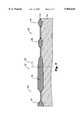
- a semiconductor structure device 12includes a core region 8 and a peripheral region 9 separated by an interface 10.
- Structure 12includes a substrate or base 14, a pad oxide layer 16, and a nitride layer 18.
- Structure 12is first etched in accordance with a preliminary mask or zero layer mask (not shown) for defining alignment marks.
- a source drain mask layer 20is provided over layer 18 to define source and drain regions in peripheral region 9.
- Layer 20completely covers core region 8.
- structure 12is etched to remove layer 18 from portions of region 9 in accordance with layer 20.
- layer 20is stripped from structure 12, and structure 12 is oxidized to form LOCOS isolation structure 24 in accordance with a conventional LOCOS technique. During this step, layer 18 in core region 8 is also oxidized. Additionally, LOCOS structure 24 is relatively thin at boundary or interface 10 with respect to the remaining portion of peripheral region 9.
- a source drain mask layer 26is applied to define source and drain regions in core region 8 as well as isolation structures for core region 8.
- structure 12is etched in accordance with layer 26 to remove portions of layer 18 in core region 8.
- portions of structure 24 close to interface 10can be etched because layer 26 does not reach interface 10 (FIG. 4).
- the etching of structure 12can thin the thickness of structure 24 in peripheral region 9. This thinning can cause a step 28 and a groove 30.
- the thickness of structure 24can be less than 1300 ⁇ at step 28.
- isolation structures 40 and 42are grown in a thermal process in accordance with a conventional LOCOS technique. Step 28 and groove 30 remain on structure 10.
- the thickness of structure 28can be less than 1000 ⁇ at groove 28.
- Step 28 and groove 30can cause residue or "stringer” problems during subsequent first polysilicon, oxygen-nitride-oxygen (ONO), second polysilicon and self-aligned etched (SAE) processes.
- Conductive material trapped in step 28, groove 30can create unintentional gate structures due to the thinness of structure 24 or can electrically short adjacent structures.
- layer 18is subjected to two oxidation steps which can create "oxide bumps" on top of "birds beaks" associated with structures 40 and 42.
- the oxide bumpscan be due to material surface stress of layer 18 which is caused by the dual oxidation process associated with the formation of structures 24, 40 and 42.
- Step 28can also create a "race track” topography problem related to the difference in thickness of structure 24 at interface 10.
- the race track topography problemis manifested when photoresist is provided on structure 12 and includes grooves or lanes in a race track form.
- the present inventionrelates to a method of fabricating an integrated circuit having a core area, an interface area and a peripheral area.
- the interface areais between the core area and the peripheral area, and the peripheral area has at least one thick LOCOS structure.
- the core areahas at least one thin LOCOS structure.
- the thin LOCOS structure and the thick LOCOS structureare formed in a semiconductor substrate.
- the semiconductor substrateincludes a first hard mask layer disposed above the substrate.
- the methodincludes a first etch resist layer over the first hard mask layer, etching the first hard mask layer in accordance with the first etch resist layer, growing the thin LOCOS structure, stripping the first hard mask layer, and providing a second hard mask layer over the core region.
- the first etch resist layerdefines the thin LOCOS structure.
- the present inventionfurther relates to a method of fabricating at least one first isolation region and at least one second isolation region on a semiconductor substrate.
- the semiconductor substrateincludes a pad oxide layer disposed above the substrate and a first hard mask layer disposed above the pad oxide layer.
- the methodincludes the steps of etching the first hard mask layer, forming the first isolation region by oxidizing the substrate, removing the first hard mask layer, and providing a second hard mask layer.
- the present inventionstill further relates to a method of fabricating a semiconductor device on a semiconductor, the method includes providing a first nitride layer over a semiconductor substrate, selectively etching the first nitride layer at a plurality of first locations, forming a plurality of first oxide isolation structures at the first locations, providing a second nitride layer over the semiconductor substrate, selectively etching the second nitride layer at a plurality of second locations, and forming a plurality of second oxide isolation structures at the second locations.
- selective oxidation structuresare provided in a core region and a peripheral region of an integrated circuit (IC). Thick oxidation structures are provided in the peripheral region, and thin oxidation structures are provided in the core region. Two separate hard mask layers, such as, nitride layers, are utilized to define the thin and thick oxidation structures. The thin oxidation structures in the core region are formed first followed by the thick oxidation structures in the peripheral region.
- ICintegrated circuit
- selective oxidation by LOCOSis utilized for thick and thin LOCOS isolation regions in a peripheral region and core region, respectively, of a semiconductor substrate.
- An interface region between the core region and peripheral regionpreferably has relatively even isolation (e.g., without significant step downs or grooves) due to the advantageous fabrication technique.
- the advantageous processreduces residue or "stringer” problems.
- the advantageous fabrication processis less susceptible to "oxide bumps" formed on oxidation structures in the core region and reduces the potential for photo resist "race track” problems.
- boron segregation into the field oxideis reduced or eliminated because the integrated circuit is implanted with boron after the formation of the field oxide.
- FIG. 1is a cross-sectional view of a semiconductor device illustrating a first step in a conventional LOCOS formation process
- FIG. 2is a cross-sectional view of the semiconductor device shown in FIG. 1 illustrating a second step in the conventional LOCOS formation process
- FIG. 3is a cross-sectional view of the semiconductor device shown in FIG. 2 illustrating a third step in the conventional LOCOS formation process
- FIG. 4is a cross-sectional view of the semiconductor device shown in FIG. 3 illustrating a fourth step in the conventional LOCOS formation process
- FIG. 5is a cross-sectional view of the semiconductor device shown in FIG. 4 illustrating a fifth step in the conventional LOCOS formation process
- FIG. 6is a cross-sectional view of the semiconductor device shown in FIG. 5 illustrating a sixth step in the conventional LOCOS formation process
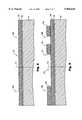
- FIG. 7is a cross-sectional view of a semiconductor structure including thin isolation structures in a core region and thick isolation structures in a peripheral region in accordance with an exemplary embodiment of the present invention
- FIG. 8is a cross-sectional view of the semiconductor structure shown in FIG. 7 illustrating a first step in the method utilized to manufacture the semiconductor structure;
- FIG. 9is a cross-sectional view of the semiconductor structure shown in FIG. 8 illustrating a second step in the method utilized to manufacture the semiconductor structure;
- FIG. 10is a cross-sectional view of the semiconductor structure shown in FIG. 9 illustrating a third step in the method utilized to manufacture the semiconductor structure;
- FIG. 11is a cross-sectional view of the semiconductor structure shown in FIG. 10 illustrating a fourth step in the method utilized to manufacture the semiconductor structure;
- FIG. 12is a cross-sectional view of the semiconductor structure shown in FIG. 11 illustrating a fifth step in the method utilized to manufacture the semiconductor structure.
- FIG. 13is a cross-sectional view of the semiconductor structure shown in FIG. 12 illustrating a sixth step in the method utilized to manufacture the semiconductor structure.
- a semiconductor device or structure 112includes a core region 108, an interface region 110, and a peripheral region 109.
- Structure 112includes a substrate or a base 114, an oxide isolation structure 142, an oxide isolation structure 144, an oxide isolation structure 146, and an oxide isolation structure 148.
- Structure 112can be any type of semiconductor device or portion thereof made from any of the various semiconductor processes, such as, complimentary metal oxide semiconductor (CMOS) process, bipolar process, or other semiconductor processes. Structure 112 is shown in FIG. 7 before other components and structures, such as, polysilicon layers, insulating layers, and metal layers are provided.
- CMOScomplimentary metal oxide semiconductor
- bipolar processbipolar process
- FIG. 7shows that other components and structures, such as, polysilicon layers, insulating layers, and metal layers are provided.
- Semiconductor structure 112may be an entire or a portion of an integrated circuit (IC) including a multitude of electronic components.
- Base 114 of semiconductor structure 112is preferably silicon or other semiconductor material and can be doped with P-type dopants or N-type dopants.
- Structure 112can include CMOS transistors fabricated in N-type and P-type wells.
- structure 112is at least a portion of a memory device, such as, a flash EEPROM.
- the memory deviceincludes memory cells provided in core region 108 and input/output or drive circuitry in peripheral region 109.
- Core region 108is a low voltage region (e.g., 2.7V or less).
- Peripheral region 109is preferably a higher voltage region (e.g., 3.3V or higher) including drive circuitry.
- Interface region 110is adjacent a border 111 between regions 108 and 109.
- Core region 108includes isolation structures 146 and 148, and peripheral region 109 includes isolation structures 142 and 144.
- Structures 146 and 148are preferably thin LOCOS structures having a thickness of 2,000 angstroms ( ⁇ ).
- Structures 142 and 144are preferably thick LOCOS structures having a thickness of 4,000 ⁇ .
- Structure 142extends across interface region 110 and into region 108.
- Structures 142, 144, 146 and 148are grown in selective thermal field oxidation processes.
- System parameters and design requirementscan define the various dimensions for structures 142, 144, 146 and 148. For example, as the size and spacing of transistors integrated within and above base 114 decrease, the width and depth of structures 142, 144, 146 and 148 can likewise decrease. Further, as voltage parameters change for the functional units integrated in base 114, the dimensional relationships of isolation structures 142, 144, 146 and 148 can also change. Thus, system configurations and fabrication parameters associated with the design of structure 112 can serve to define the dimensions of structures 142, 144, 146 and 148, as well as, regions 108, 109 and 110.
- semiconductor structure 112includes substrate layer or base 114, an oxide film or pad oxide layer 116, and a nitride layer 118.
- Base 114is preferably silicon (Si) and can be doped with phosphorous for N-type wells or boron for P-type wells and is significantly thicker than layers 116 and 118.
- Pad oxide layer 116is grown on top of base 114 to a thickness of approximately 150-250 ⁇ by a thermal process.
- Nitride layer 118is deposited as a 1,700 ⁇ thick layer by chemical vapor deposition (CVD) on top of pad oxide layer 116.
- CVDchemical vapor deposition
- layers 116 and 118may be deposited by physical vapor deposition (PVD), sputtering deposition, collimated sputtering deposition, dipping, evaporating, or other application techniques.
- Nitride layer 118is a hard mask layer.
- Layer 118is comprised of silicon nitride (Si 3 N 4 ) and serves to prevent oxidation of underlying substrate 114.
- Layer 118is also an anti-reflective coating.
- Pad oxide layer 116provides stress relief between base 114 and layer 118 for structure 112.
- layer 118can be any hard mask layer.
- an etch resist layer 152is selectively applied on top of layer 118.
- Etch resist layer 152is preferably a photoresist layer which defines spacings 154 for structures 142, 146 and 148. Unlike conventional processes, well regions are not yet defined in regions 108 and 109.
- Structure 112can be etched by dry etching (e.g., plasma etching) to form spacings 156 in layer 118 (FIG. 10). This etching of structure 112 can also serve to define alignment marks for structure 112, thereby eliminating the need for a zero mask layer.
- Layer 152(FIG. 9) is removed or stripped from structure 112. With reference to FIG.
- structure 112is oxidized to form structures 142, 146, and 148 in accordance with a LOCOS process.
- Structures 142, 146 and 148are grown to a 1000 ⁇ to 3000 ⁇ thickness, preferably 2000 ⁇ to 2500 ⁇ or less.
- nitride layer 118is removed or stripped. Layer 118 can be removed by a hot phosphoric acid wet strip process, other etching processes, or other removal processes.
- a hard mask or nitride layer 160is deposited over structures 142, 146 and 148 and layer 116.
- Layer 160is preferably similar to layer 118 (in FIG. 10) and has a thickness of 1700 ⁇ .
- Etch resist layer 162is provided over layer 160.
- Etch resist layer 162is preferably a photoresist layer which is selectively provided to define structure 142 and structure 144 with spacings 166.
- Layer 162preferably completely covers region 108.
- layer 160is etched to define spacings 168.
- structure 112undergoes a thermal process in accordance with a LOCOS technique to form structures 144 and 142 (FIG. 7).
- structures 144 and 142are grown to a thickness of 4000 ⁇ in peripheral region 109.
- Layer 160 in region 108prevents further growth of structures, 146 and 148 during this second LOCOS process.
- Structure 142grows to an edge 168 (FIG. 13) of layer 160.
- layer 160is stripped by a hot phosphoric acid wet strip process. Alternatively, other etching or removal techniques can be utilized to remove layer 160.
- structures 144 and 142have a relatively even thickness when compared to structure 24 (FIG. 6).
- Structure 142has a relatively even thickness throughout interface region 110.
- the use of two hard mask layers 118 and 160advantageously eliminates or reduces residue or stringer problems associated with the conventional process discussed with reference to FIGS. 1-6. Accordingly, structure 112 can optimize isolation structure thicknesses associated with structures 142, 144, 146 and 148 because overetching problems are significantly reduced.
- source drain definitions in core region 108can be used as a target for follow-up deep N-well, P-well and N-well implant masks, thereby eliminating the need for a zero layer mask.
- the process discussed with reference to FIGS. 7-13reduces the "oxide" bump concern because each nitride layer 118 and 160 is only subjected to a single oxidation process. Therefore, the method advantageously eliminates material surface stress which can cause field edge defects in core region 8 due to oxidized nitride in core region 108. Further, the method reduces non-uniform "race track" problems due to topographic differences in field oxide thickness of structure 142 at interface region 110.
Landscapes
- Engineering & Computer Science (AREA)
- Physics & Mathematics (AREA)
- Condensed Matter Physics & Semiconductors (AREA)
- General Physics & Mathematics (AREA)
- Manufacturing & Machinery (AREA)
- Computer Hardware Design (AREA)
- Microelectronics & Electronic Packaging (AREA)
- Power Engineering (AREA)
- Element Separation (AREA)
- Local Oxidation Of Silicon (AREA)
- Metal-Oxide And Bipolar Metal-Oxide Semiconductor Integrated Circuits (AREA)
Abstract
Description
Claims (20)
Priority Applications (6)
| Application Number | Priority Date | Filing Date | Title |
|---|---|---|---|
| US09/036,288US5966618A (en) | 1998-03-06 | 1998-03-06 | Method of forming dual field isolation structures |
| PCT/US1999/004905WO1999045589A1 (en) | 1998-03-06 | 1999-03-05 | Method of forming dual field isolation structures |
| EP99911155AEP1060510B1 (en) | 1998-03-06 | 1999-03-05 | Method of forming dual field isolation structures |
| KR10-2000-7009845AKR100537812B1 (en) | 1998-03-06 | 1999-03-05 | Method of forming dual field isolation structures |
| DE69939775TDE69939775D1 (en) | 1998-03-06 | 1999-03-05 | PROCESS FOR FOR FORMING DOUBLE FIELD OXIDE STRUCTURES |
| JP2000535047AJP2002506288A (en) | 1998-03-06 | 1999-03-05 | Method of forming a dual field isolation structure |
Applications Claiming Priority (1)
| Application Number | Priority Date | Filing Date | Title |
|---|---|---|---|
| US09/036,288US5966618A (en) | 1998-03-06 | 1998-03-06 | Method of forming dual field isolation structures |
Publications (1)
| Publication Number | Publication Date |
|---|---|
| US5966618Atrue US5966618A (en) | 1999-10-12 |
Family
ID=21887749
Family Applications (1)
| Application Number | Title | Priority Date | Filing Date |
|---|---|---|---|
| US09/036,288Expired - LifetimeUS5966618A (en) | 1998-03-06 | 1998-03-06 | Method of forming dual field isolation structures |
Country Status (6)
| Country | Link |
|---|---|
| US (1) | US5966618A (en) |
| EP (1) | EP1060510B1 (en) |
| JP (1) | JP2002506288A (en) |
| KR (1) | KR100537812B1 (en) |
| DE (1) | DE69939775D1 (en) |
| WO (1) | WO1999045589A1 (en) |
Cited By (11)
| Publication number | Priority date | Publication date | Assignee | Title |
|---|---|---|---|---|
| US6127247A (en)* | 1998-06-03 | 2000-10-03 | Texas Instruments - Acer Incorporated | Method of eliminating photoresist outgassing in constructing CMOS vertically modulated wells by high energy ion implantation |
| US6249036B1 (en)* | 1998-03-18 | 2001-06-19 | Advanced Micro Devices, Inc. | Stepper alignment mark formation with dual field oxide process |
| US6362049B1 (en)* | 1998-12-04 | 2002-03-26 | Advanced Micro Devices, Inc. | High yield performance semiconductor process flow for NAND flash memory products |
| US6383861B1 (en)* | 1999-02-18 | 2002-05-07 | Micron Technology, Inc. | Method of fabricating a dual gate dielectric |
| US6750157B1 (en) | 2000-10-12 | 2004-06-15 | Advanced Micro Devices, Inc. | Nonvolatile memory cell with a nitridated oxide layer |
| US20050199939A1 (en)* | 2004-03-12 | 2005-09-15 | Lutze Jeffrey W. | Self aligned non-volatile memory cells and processes for fabrication |
| US20050207226A1 (en)* | 2002-10-09 | 2005-09-22 | Yuan Jack H | Flash memory array with increased coupling between floating and control gates |
| US20060134845A1 (en)* | 2004-12-22 | 2006-06-22 | Tuan Pham | Low-voltage, multiple thin-gate oxide and low-resistance gate electrode |
| US20060134864A1 (en)* | 2004-12-22 | 2006-06-22 | Masaaki Higashitani | Multi-thickness dielectric for semiconductor memory |
| US20070087504A1 (en)* | 2005-10-18 | 2007-04-19 | Pham Tuan D | Integration process flow for flash devices with low gap fill aspect ratio |
| US20200185513A1 (en)* | 2018-12-06 | 2020-06-11 | Nexperia B.V. | Semiconductor device and method of manufacture |
Families Citing this family (2)
| Publication number | Priority date | Publication date | Assignee | Title |
|---|---|---|---|---|
| FR2810447B1 (en)* | 2000-06-16 | 2003-09-05 | Commissariat Energie Atomique | METHOD FOR CREATING AN INTEGRATED CIRCUIT FLOOR OR CONTAINING FINE AND BROAD REASONS |
| ATE556020T1 (en)* | 2004-12-29 | 2012-05-15 | Otis Elevator Co | BALANCING IN AN ELEVATOR SYSTEM WITH MULTIPLE CABINS IN A SINGLE SHAFT |
Citations (7)
| Publication number | Priority date | Publication date | Assignee | Title |
|---|---|---|---|---|
| US5110756A (en)* | 1991-07-03 | 1992-05-05 | At&T Bell Laboratories | Method of semiconductor integrated circuit manufacturing which includes processing for reducing defect density |
| US5128274A (en)* | 1989-08-01 | 1992-07-07 | Matsushita Electric Industrial Co., Ltd. | Method for producing a semiconductor device having a LOCOS insulating film with at least two different thickness |
| US5316966A (en)* | 1990-09-28 | 1994-05-31 | U.S. Philips Corporation | Method of providing mask alignment marks |
| US5466623A (en)* | 1987-07-01 | 1995-11-14 | Mitsubishi Denki Kabushiki Kaisha | Method of making semiconductor integrated circuit having isolation oxide regions with different thickness |
| US5646063A (en)* | 1996-03-28 | 1997-07-08 | Advanced Micro Devices, Inc. | Hybrid of local oxidation of silicon isolation and trench isolation for a semiconductor device |
| US5786264A (en)* | 1995-12-29 | 1998-07-28 | Lg Semicon Co., Ltd. | Method of forming isolation layer of semiconductor elements |
| US5794809A (en)* | 1997-02-18 | 1998-08-18 | Shuval; Shlomo | Trash container with automatic liner bag feed |
Family Cites Families (6)
| Publication number | Priority date | Publication date | Assignee | Title |
|---|---|---|---|---|
| DE3318213A1 (en)* | 1983-05-19 | 1984-11-22 | Deutsche Itt Industries Gmbh, 7800 Freiburg | METHOD FOR PRODUCING AN INTEGRATED INSULATION LAYER FIELD EFFECT TRANSISTOR WITH CONTACTS FOR THE GATE ELECTRODE SELF-ALIGNED |
| JPS62183164A (en)* | 1986-02-07 | 1987-08-11 | Hitachi Ltd | Semiconductor memory device and manufacture thereof |
| JPS6442164A (en)* | 1987-08-07 | 1989-02-14 | Fujitsu Ltd | Semiconductor device and manufacture thereof |
| JPH04111465A (en)* | 1990-08-31 | 1992-04-13 | Fujitsu Ltd | Manufacture of non-volatile semiconductor memory device |
| JPH08125006A (en)* | 1994-10-20 | 1996-05-17 | Victor Co Of Japan Ltd | Semiconductor device and its manufacture |
| JPH0997788A (en)* | 1995-07-21 | 1997-04-08 | Rohm Co Ltd | Semiconductor device and manufacture thereof |
- 1998
- 1998-03-06USUS09/036,288patent/US5966618A/ennot_activeExpired - Lifetime
- 1999
- 1999-03-05WOPCT/US1999/004905patent/WO1999045589A1/enactiveIP Right Grant
- 1999-03-05JPJP2000535047Apatent/JP2002506288A/enactivePending
- 1999-03-05DEDE69939775Tpatent/DE69939775D1/ennot_activeExpired - Lifetime
- 1999-03-05KRKR10-2000-7009845Apatent/KR100537812B1/ennot_activeExpired - Fee Related
- 1999-03-05EPEP99911155Apatent/EP1060510B1/ennot_activeExpired - Lifetime
Patent Citations (7)
| Publication number | Priority date | Publication date | Assignee | Title |
|---|---|---|---|---|
| US5466623A (en)* | 1987-07-01 | 1995-11-14 | Mitsubishi Denki Kabushiki Kaisha | Method of making semiconductor integrated circuit having isolation oxide regions with different thickness |
| US5128274A (en)* | 1989-08-01 | 1992-07-07 | Matsushita Electric Industrial Co., Ltd. | Method for producing a semiconductor device having a LOCOS insulating film with at least two different thickness |
| US5316966A (en)* | 1990-09-28 | 1994-05-31 | U.S. Philips Corporation | Method of providing mask alignment marks |
| US5110756A (en)* | 1991-07-03 | 1992-05-05 | At&T Bell Laboratories | Method of semiconductor integrated circuit manufacturing which includes processing for reducing defect density |
| US5786264A (en)* | 1995-12-29 | 1998-07-28 | Lg Semicon Co., Ltd. | Method of forming isolation layer of semiconductor elements |
| US5646063A (en)* | 1996-03-28 | 1997-07-08 | Advanced Micro Devices, Inc. | Hybrid of local oxidation of silicon isolation and trench isolation for a semiconductor device |
| US5794809A (en)* | 1997-02-18 | 1998-08-18 | Shuval; Shlomo | Trash container with automatic liner bag feed |
Cited By (25)
| Publication number | Priority date | Publication date | Assignee | Title |
|---|---|---|---|---|
| US6249036B1 (en)* | 1998-03-18 | 2001-06-19 | Advanced Micro Devices, Inc. | Stepper alignment mark formation with dual field oxide process |
| US6420224B2 (en)* | 1998-03-18 | 2002-07-16 | Advanced Micro Devices, Inc. | Stepper alignment mark formation with dual field oxide process |
| US6127247A (en)* | 1998-06-03 | 2000-10-03 | Texas Instruments - Acer Incorporated | Method of eliminating photoresist outgassing in constructing CMOS vertically modulated wells by high energy ion implantation |
| US6362049B1 (en)* | 1998-12-04 | 2002-03-26 | Advanced Micro Devices, Inc. | High yield performance semiconductor process flow for NAND flash memory products |
| US6946713B2 (en) | 1999-02-18 | 2005-09-20 | Micron Technology, Inc. | Multiple thickness gate dielectric layers |
| US6383861B1 (en)* | 1999-02-18 | 2002-05-07 | Micron Technology, Inc. | Method of fabricating a dual gate dielectric |
| US6653675B2 (en) | 1999-02-18 | 2003-11-25 | Micron Technology, Inc. | Dual gate dielectric construction |
| US20040113229A1 (en)* | 1999-02-18 | 2004-06-17 | Fernando Gonzalez | Dual gate dielectric construction |
| US6750157B1 (en) | 2000-10-12 | 2004-06-15 | Advanced Micro Devices, Inc. | Nonvolatile memory cell with a nitridated oxide layer |
| US20070122980A1 (en)* | 2002-10-09 | 2007-05-31 | Yuan Jack H | Flash Memory Array with Increased Coupling Between Floating and Control Gates |
| US7170131B2 (en) | 2002-10-09 | 2007-01-30 | Sandisk Corporation | Flash memory array with increased coupling between floating and control gates |
| US7517756B2 (en) | 2002-10-09 | 2009-04-14 | Sandisk Corporation | Flash memory array with increased coupling between floating and control gates |
| US20050207226A1 (en)* | 2002-10-09 | 2005-09-22 | Yuan Jack H | Flash memory array with increased coupling between floating and control gates |
| US7436019B2 (en) | 2004-03-12 | 2008-10-14 | Sandisk Corporation | Non-volatile memory cells shaped to increase coupling to word lines |
| US7183153B2 (en) | 2004-03-12 | 2007-02-27 | Sandisk Corporation | Method of manufacturing self aligned non-volatile memory cells |
| US20070111422A1 (en)* | 2004-03-12 | 2007-05-17 | Lutze Jeffrey W | Self Aligned Non-Volatile Memory Cells and Processes for Fabrication |
| US20050199939A1 (en)* | 2004-03-12 | 2005-09-15 | Lutze Jeffrey W. | Self aligned non-volatile memory cells and processes for fabrication |
| US7202125B2 (en) | 2004-12-22 | 2007-04-10 | Sandisk Corporation | Low-voltage, multiple thin-gate oxide and low-resistance gate electrode |
| US20060134864A1 (en)* | 2004-12-22 | 2006-06-22 | Masaaki Higashitani | Multi-thickness dielectric for semiconductor memory |
| US7482223B2 (en) | 2004-12-22 | 2009-01-27 | Sandisk Corporation | Multi-thickness dielectric for semiconductor memory |
| US20060134845A1 (en)* | 2004-12-22 | 2006-06-22 | Tuan Pham | Low-voltage, multiple thin-gate oxide and low-resistance gate electrode |
| US20070087504A1 (en)* | 2005-10-18 | 2007-04-19 | Pham Tuan D | Integration process flow for flash devices with low gap fill aspect ratio |
| US7541240B2 (en) | 2005-10-18 | 2009-06-02 | Sandisk Corporation | Integration process flow for flash devices with low gap fill aspect ratio |
| US20200185513A1 (en)* | 2018-12-06 | 2020-06-11 | Nexperia B.V. | Semiconductor device and method of manufacture |
| US11996474B2 (en)* | 2018-12-06 | 2024-05-28 | Nexperia B.V. | Semiconductor device and method of manufacture |
Also Published As
| Publication number | Publication date |
|---|---|
| KR20010041645A (en) | 2001-05-25 |
| EP1060510B1 (en) | 2008-10-22 |
| EP1060510A1 (en) | 2000-12-20 |
| WO1999045589A1 (en) | 1999-09-10 |
| KR100537812B1 (en) | 2005-12-20 |
| DE69939775D1 (en) | 2008-12-04 |
| JP2002506288A (en) | 2002-02-26 |
Similar Documents
| Publication | Publication Date | Title |
|---|---|---|
| US7588973B2 (en) | Semiconductor device and method of manufacturing the same | |
| EP1487011B1 (en) | Integrated circuits having adjacent regions having shallow trench isolation structures without liner layers therein therebetween and methods of forming same | |
| US6921947B2 (en) | Semiconductor device having recessed isolation insulation film | |
| GB2179788A (en) | Isolation structure in semiconductor devices | |
| US6579764B2 (en) | Integrated circuit memory devices having non-volatile memory transistors and methods of fabricating the same | |
| US8325516B2 (en) | Semiconductor device with split gate memory cell and fabrication method thereof | |
| US7410874B2 (en) | Method of integrating triple gate oxide thickness | |
| US5966618A (en) | Method of forming dual field isolation structures | |
| JP2000036546A (en) | Non-volatile semiconductor memory and its manufacture | |
| US20070241373A1 (en) | Semiconductor Device and Its Manufacturing Method | |
| US6897516B2 (en) | Flash memory array structure and method of forming | |
| US20050059215A1 (en) | Semiconductor device with dual gate oxides | |
| US5374584A (en) | Method for isolating elements in a semiconductor chip | |
| US6472259B1 (en) | Method of manufacturing semiconductor device | |
| US6534364B1 (en) | Tunnel diode layout for an EEPROM cell for protecting the tunnel diode region | |
| US20040082132A1 (en) | Integration of semiconductor on implanted insulator | |
| EP1246237A2 (en) | A method of forming isolation trenches between active regions for an E2PROM cell | |
| US20030100166A1 (en) | Method for avoiding the effects of lack of uniformity in trench isolated integrated circuits | |
| JPH0888360A (en) | Semiconductor device and manufacturing method thereof | |
| US5981358A (en) | Encroachless LOCOS isolation | |
| KR100360075B1 (en) | Manufacturing method of high performance bipolar transistor in BICMOS process | |
| JPH0218587B2 (en) | ||
| JPH1187661A (en) | Semiconductor device and manufacturing method thereof | |
| KR20010059737A (en) | Method for forming isolation layer of semiconductor device | |
| KR20010064441A (en) | Method of forming trench isolation layer in semiconductor device |
Legal Events
| Date | Code | Title | Description |
|---|---|---|---|
| AS | Assignment | Owner name:ADVANCED MICRO DEVICES, CALIFORNIA Free format text:ASSIGNMENT OF ASSIGNORS INTEREST;ASSIGNORS:SUN, YA;PHAM, TUAN D.;RAMSBEY, MARK S.;AND OTHERS;REEL/FRAME:009065/0575;SIGNING DATES FROM 19980227 TO 19980303 | |
| STCF | Information on status: patent grant | Free format text:PATENTED CASE | |
| CC | Certificate of correction | ||
| FPAY | Fee payment | Year of fee payment:4 | |
| FPAY | Fee payment | Year of fee payment:8 | |
| AS | Assignment | Owner name:GLOBALFOUNDRIES INC., CAYMAN ISLANDS Free format text:ASSIGNMENT OF ASSIGNORS INTEREST;ASSIGNOR:AMD TECHNOLOGIES HOLDINGS, INC.;REEL/FRAME:022764/0544 Effective date:20090302 Owner name:AMD TECHNOLOGIES HOLDINGS, INC., CALIFORNIA Free format text:ASSIGNMENT OF ASSIGNORS INTEREST;ASSIGNOR:ADVANCED MICRO DEVICES, INC.;REEL/FRAME:022764/0488 Effective date:20090302 | |
| FPAY | Fee payment | Year of fee payment:12 | |
| AS | Assignment | Owner name:GLOBALFOUNDRIES U.S. INC., NEW YORK Free format text:RELEASE BY SECURED PARTY;ASSIGNOR:WILMINGTON TRUST, NATIONAL ASSOCIATION;REEL/FRAME:056987/0001 Effective date:20201117 |