US5966323A - Low switching field magnetoresistive tunneling junction for high density arrays - Google Patents
Low switching field magnetoresistive tunneling junction for high density arraysDownload PDFInfo
- Publication number
- US5966323A US5966323AUS08/993,768US99376897AUS5966323AUS 5966323 AUS5966323 AUS 5966323AUS 99376897 AUS99376897 AUS 99376897AUS 5966323 AUS5966323 AUS 5966323A
- Authority
- US
- United States
- Prior art keywords
- layer
- magnetic
- magnetoresistive
- layers
- tunneling junction
- Prior art date
- Legal status (The legal status is an assumption and is not a legal conclusion. Google has not performed a legal analysis and makes no representation as to the accuracy of the status listed.)
- Expired - Lifetime
Links
- 230000005641tunnelingEffects0.000titleclaimsabstractdescription41
- 238000003491arrayMethods0.000titledescription4
- 230000005291magnetic effectEffects0.000claimsabstractdescription147
- 239000013598vectorSubstances0.000claimsabstractdescription62
- 230000015654memoryEffects0.000claimsabstractdescription50
- 230000003993interactionEffects0.000claimsabstractdescription32
- 239000012777electrically insulating materialSubstances0.000claimsabstractdescription6
- 239000000463materialSubstances0.000claimsdescription18
- 230000008878couplingEffects0.000claimsdescription15
- 238000010168coupling processMethods0.000claimsdescription15
- 238000005859coupling reactionMethods0.000claimsdescription15
- 239000000758substrateSubstances0.000claimsdescription13
- 230000004907fluxEffects0.000claimsdescription11
- 239000002885antiferromagnetic materialSubstances0.000claimsdescription8
- 229910015136FeMnInorganic materials0.000claimsdescription3
- 229910003289NiMnInorganic materials0.000claimsdescription3
- 239000010410layerSubstances0.000description169
- 230000005415magnetizationEffects0.000description9
- 230000008859changeEffects0.000description7
- 238000004519manufacturing processMethods0.000description5
- PXHVJJICTQNCMI-UHFFFAOYSA-NNickelChemical compound[Ni]PXHVJJICTQNCMI-UHFFFAOYSA-N0.000description4
- 230000005290antiferromagnetic effectEffects0.000description4
- FQMNUIZEFUVPNU-UHFFFAOYSA-Ncobalt ironChemical compound[Fe].[Co].[Co]FQMNUIZEFUVPNU-UHFFFAOYSA-N0.000description4
- 230000008021depositionEffects0.000description4
- 239000000696magnetic materialSubstances0.000description4
- XEEYBQQBJWHFJM-UHFFFAOYSA-NIronChemical compound[Fe]XEEYBQQBJWHFJM-UHFFFAOYSA-N0.000description3
- 229910045601alloyInorganic materials0.000description3
- 239000000956alloySubstances0.000description3
- 239000010432diamondSubstances0.000description3
- 230000000694effectsEffects0.000description3
- 239000004065semiconductorSubstances0.000description3
- 229910001030Iron–nickel alloyInorganic materials0.000description2
- KDLHZDBZIXYQEI-UHFFFAOYSA-NPalladiumChemical compound[Pd]KDLHZDBZIXYQEI-UHFFFAOYSA-N0.000description2
- KGWWEXORQXHJJQ-UHFFFAOYSA-N[Fe].[Co].[Ni]Chemical compound[Fe].[Co].[Ni]KGWWEXORQXHJJQ-UHFFFAOYSA-N0.000description2
- 229910017052cobaltInorganic materials0.000description2
- 239000010941cobaltSubstances0.000description2
- GUTLYIVDDKVIGB-UHFFFAOYSA-Ncobalt atomChemical compound[Co]GUTLYIVDDKVIGB-UHFFFAOYSA-N0.000description2
- 239000013078crystalSubstances0.000description2
- 238000010586diagramMethods0.000description2
- 230000005294ferromagnetic effectEffects0.000description2
- 239000011229interlayerSubstances0.000description2
- 229910052742ironInorganic materials0.000description2
- 229910001004magnetic alloyInorganic materials0.000description2
- 238000000034methodMethods0.000description2
- 230000004048modificationEffects0.000description2
- 238000012986modificationMethods0.000description2
- 229910052759nickelInorganic materials0.000description2
- BASFCYQUMIYNBI-UHFFFAOYSA-NplatinumChemical compound[Pt]BASFCYQUMIYNBI-UHFFFAOYSA-N0.000description2
- 125000006850spacer groupChemical group0.000description2
- 229910018404Al2 O3Inorganic materials0.000description1
- 229910003321CoFeInorganic materials0.000description1
- RYGMFSIKBFXOCR-UHFFFAOYSA-NCopperChemical compound[Cu]RYGMFSIKBFXOCR-UHFFFAOYSA-N0.000description1
- 230000009471actionEffects0.000description1
- 238000000137annealingMethods0.000description1
- 230000004888barrier functionEffects0.000description1
- 230000015572biosynthetic processEffects0.000description1
- 239000002131composite materialSubstances0.000description1
- 229910052802copperInorganic materials0.000description1
- 239000010949copperSubstances0.000description1
- 238000005090crystal fieldMethods0.000description1
- 230000007423decreaseEffects0.000description1
- 229910003460diamondInorganic materials0.000description1
- 239000003989dielectric materialSubstances0.000description1
- 238000005516engineering processMethods0.000description1
- 238000005530etchingMethods0.000description1
- 239000003302ferromagnetic materialSubstances0.000description1
- UGKDIUIOSMUOAW-UHFFFAOYSA-Niron nickelChemical compound[Fe].[Ni]UGKDIUIOSMUOAW-UHFFFAOYSA-N0.000description1
- 230000005381magnetic domainEffects0.000description1
- 150000004767nitridesChemical class0.000description1
- 239000012811non-conductive materialSubstances0.000description1
- TWNQGVIAIRXVLR-UHFFFAOYSA-Noxo(oxoalumanyloxy)alumaneChemical compoundO=[Al]O[Al]=OTWNQGVIAIRXVLR-UHFFFAOYSA-N0.000description1
- 229910052763palladiumInorganic materials0.000description1
- 230000002093peripheral effectEffects0.000description1
- 229910052697platinumInorganic materials0.000description1
- 239000002356single layerSubstances0.000description1
- 230000007704transitionEffects0.000description1
Images


Classifications
- G—PHYSICS
- G11—INFORMATION STORAGE
- G11C—STATIC STORES
- G11C11/00—Digital stores characterised by the use of particular electric or magnetic storage elements; Storage elements therefor
- G11C11/02—Digital stores characterised by the use of particular electric or magnetic storage elements; Storage elements therefor using magnetic elements
- G11C11/16—Digital stores characterised by the use of particular electric or magnetic storage elements; Storage elements therefor using magnetic elements using elements in which the storage effect is based on magnetic spin effect
- G11C11/161—Digital stores characterised by the use of particular electric or magnetic storage elements; Storage elements therefor using magnetic elements using elements in which the storage effect is based on magnetic spin effect details concerning the memory cell structure, e.g. the layers of the ferromagnetic memory cell
- G—PHYSICS
- G11—INFORMATION STORAGE
- G11C—STATIC STORES
- G11C11/00—Digital stores characterised by the use of particular electric or magnetic storage elements; Storage elements therefor
- G11C11/02—Digital stores characterised by the use of particular electric or magnetic storage elements; Storage elements therefor using magnetic elements
- G11C11/16—Digital stores characterised by the use of particular electric or magnetic storage elements; Storage elements therefor using magnetic elements using elements in which the storage effect is based on magnetic spin effect
- G11C11/165—Auxiliary circuits
- G11C11/1659—Cell access
- G—PHYSICS
- G11—INFORMATION STORAGE
- G11C—STATIC STORES
- G11C11/00—Digital stores characterised by the use of particular electric or magnetic storage elements; Storage elements therefor
- G11C11/02—Digital stores characterised by the use of particular electric or magnetic storage elements; Storage elements therefor using magnetic elements
- G11C11/16—Digital stores characterised by the use of particular electric or magnetic storage elements; Storage elements therefor using magnetic elements using elements in which the storage effect is based on magnetic spin effect
- G11C11/165—Auxiliary circuits
- G11C11/1675—Writing or programming circuits or methods
- G—PHYSICS
- G11—INFORMATION STORAGE
- G11C—STATIC STORES
- G11C11/00—Digital stores characterised by the use of particular electric or magnetic storage elements; Storage elements therefor
- G11C11/56—Digital stores characterised by the use of particular electric or magnetic storage elements; Storage elements therefor using storage elements with more than two stable states represented by steps, e.g. of voltage, current, phase, frequency
- G11C11/5607—Digital stores characterised by the use of particular electric or magnetic storage elements; Storage elements therefor using storage elements with more than two stable states represented by steps, e.g. of voltage, current, phase, frequency using magnetic storage elements
- G—PHYSICS
- G11—INFORMATION STORAGE
- G11C—STATIC STORES
- G11C2211/00—Indexing scheme relating to digital stores characterized by the use of particular electric or magnetic storage elements; Storage elements therefor
- G11C2211/56—Indexing scheme relating to G11C11/56 and sub-groups for features not covered by these groups
- G11C2211/561—Multilevel memory cell aspects
- G11C2211/5615—Multilevel magnetic memory cell using non-magnetic non-conducting interlayer, e.g. MTJ
Definitions
- the present inventionpertains to magnetoresistive tunneling junctions for memory cells and more specifically to very small tunneling junctions for very high density arrays of memory cells.
- a magnetic random access memoryis a non-volatile memory which basically includes a giant magnetoresistive (GMR) material or magnetoresistive tunneling junction (MTJ) structure, a sense line, and a word line.
- the MRAMemploys the GMR effect to store memory states.
- Magnetic vectors in one or all of the layers of GMR material or MTJare switched very quickly from one direction to an opposite direction when a magnetic field is applied to the GMR material over a certain threshold.
- statesare stored, for example, one direction can be defined as a logic "0", and another direction can be defined as a logic "1".
- the GMR material or MTJmaintains these states even without a magnetic field being applied.
- the states stored in the GMR material or MTJcan be read by passing a sense current through the cell in a sense line because of the difference between the resistances of the two states.
- a dummy magnetic layeris added to a two magnetic layer stack and coupled to one of the two magnetic layers so that the other magnetic layer is a free layer.
- a drawback of the dummy magnetic layer approachis that it relies on cancellation of magnetostatic interaction between the two magnetic layers and this magnetostatic interaction strength depends on the geometry of the cell and the interlayer spacing. These parameters change as the critical dimension shrinks.
- two layer magnetic memory cellse.g. standard tunneling cells
- the aspect ratiogoes below 5
- the amount of magnetic field required for switching states of the cellincreases dramatically.
- a low switching field magnetoresistive tunneling junction memory cellincluding a first exchange coupled multi-layer structure having a pair of magnetoresistive layers with an exchange interaction layer situated in parallel juxtaposition between the pair of magnetoresistive layers.
- the pair of magnetoresistive layers in the first structureeach have a magnetic vector and the magnetic vectors are always pinned anti-parallel by coupling of the exchange interaction layer.
- the cellfurther includes a second exchange coupled multi-layer structure having a pair of magnetoresistive layers with an exchange interaction layer situated in parallel juxtaposition between the pair of magnetoresistive layers.
- the pair of magnetoresistive layers in the second structureeach have a magnetic vector and the magnetic vectors are always pinned anti-parallel by coupling of the exchange interaction layer.
- electrically insulating materialis situated in parallel juxtaposition between the first and second exchange coupled multi-layer structures to form a magnetoresistive tunneling junction.
- Each of the first and second structureshave no net magnetic moment and, hence, the memory cell has no net magnetic moment so that it can be positioned closer to adjacent cells without affecting adjacent cells.
- FIG. 1is a simplified side view of a multi-layer tunneling magnetic memory cell
- FIG. 2is a graph generally illustrating switching characteristics of the cell of FIG. 1;
- FIG. 3is a graph illustrating the actual magnetic field required to switch the upper and lower layers, respectively, versus the length/width ratio of a magnetic cell, such as the cell illustrated in FIG. 1, with a fixed width;
- FIG. 4is a graph illustrating the switching field required to write a cell versus the width of the cell
- FIGS. 5-7are plan views of different potential embodiments in accordance with the present invention for magnetic cells having low aspect ratios
- FIG. 8is a simplified side view of a multi-layer tunneling magnetic memory cell in accordance with the present invention.
- FIG. 9is a vector diagram illustrating the operation of the cell of FIG. 8;
- FIG. 10is a simplified side view of an other multi-layer tunneling magnetic memory cell in accordance with the present invention.
- FIG. 11is a simplified view in top plan of a high density array of multi-layer tunneling magnetic memory cells in accordance with the present invention.
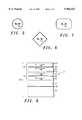
- FIG. 1illustrates an enlarged, simplified side view of a magnetic memory cell 10 having multiple layers that are ferromagnetically coupled.
- a simplified cell 10is included for purposes of explaining the operation of tunneling junctions and especially tunneling junctions with low aspect ratios.
- Cell 10includes a first magnetic layer 11 and a second magnetic layer 13, which are separated by an insulating spacer layer 12.
- Magnetic layers 11 and 13each can be single layers of ferromagnetic materials such as a layer of nickel, iron, cobalt, or alloys thereof including alloys having palladium or platinum therein.
- either of layers 11 and 13can be a composite ferromagnetic layer, such as a layer of nickel-iron-cobalt covering a layer of cobalt-iron or three layer structures including layers of cobalt-iron and nickel-iron-cobalt and cobalt-iron with cobalt-iron at the interface with adjacent layers.
- Materials that are suitable for layer 12include most non-conductive materials such as oxides, nitrides, dielectrics, etc.
- cell 10can have more than a single tunneling junction including third and fourth magnetic layers (not shown), that typically are similar to layers 11 and 13 but may be formed of different materials or have different thicknesses, and are separated by non-conductive spacer layers, (not shown) that are similar to layer 12.
- third and fourth magnetic layerstypically are similar to layers 11 and 13 but may be formed of different materials or have different thicknesses, and are separated by non-conductive spacer layers, (not shown) that are similar to layer 12.
- layers 11 and 13are rectangular and each have magnetization vectors 21 that are positioned substantially along the length of the cell and maintained parallel to the length by the physical anisotropy.
- the widthis formed to be smaller than the width of the magnetic domain walls or transition width within layers 11 and 13 and, consequently, vectors 21 can not be parallel to the width.
- widths of less than 1.0 to 1.2 micronsresult in such a constraint.
- the widthis less than one micron and is as small as can be made by manufacturing technology, and the length is greater than the width.
- thicknesses 23 and 24are approximately three to ten nanometers and thicknesses 23 and 24 may be different in some embodiments. The difference in thicknesses 23 and 24 affect the switching points of layers 11 and 13 and are utilized in some structures for reading and writing cells.
- vectors 21 and 22 in layers 11 and 13represent two different states of magnetization within cell 10. It should be understood that these are the same vectors and that they are given different numbers only to indicate different states.
- One stateis referred to as a logic "0" and the other state is a logic "1". While it will be understood by those skilled in the art that any logic definition can be assigned to either state, in this example when vectors 21 of layers 11 and 13 both point to the left in FIG. 1, cell 10 is in a logic "1" state and when vectors 22 in both layers 11 and 13 are in the opposite direction cell 10 is in a logic "0" state.
- magnetization vectors in both layers 11 and 13point in a first direction and for a second state, magnetization vectors in both layers 11 and 13 point in an opposite direction. Also, because layers 11 and 13 are ferromagnetically coupled the magnetic vectors of layers 11 and 13 are always pointing in the same direction (parallel) when no (or a very small) magnetic field is applied to cell 10. The magnetic vectors are only pointing in opposite directions (antiparallel) when specific magnetic fields are applied to cell 10, as will be explained in more detail presently.
- layer 12is an insulating layer, the provision of which between ferromagnetic layers 11 and 13 produces a tunneling junction that allows a flow of current perpendicularly through layer 12, from layer 11 to layer 13 (or vice versa).
- cell 10appears as a relatively high impedance (referred to herein as a resistance R), which has dependence on the square area of the cell and the dielectric structure, generally several thousand ohms, e.g. 5 to 6 kohms.
- the resistance R of cell 10drops perceptibly, as illustrated in FIG. 2.
- layer 11is formed of cobalt (Co) approximately 50 ⁇ thick
- layer 12is formed of aluminum oxide (Al 2 O 3 ) approximately 20 ⁇ thick
- layer 13is formed of nickel iron (NiFe) approximately 50 ⁇ thick.
- the change of resistance versus the resistance ( ⁇ R/R)is approximately 15% in the present specific example.
- the state of cell 10is relatively easily sensed by passing a sense current therethrough from layer 11 to layer 13 (or vice versa).
- the change of resistance in cell 10is easily read as a change in voltage drop across cell 10 which can conveniently be used in conjunction with memory arrays and the like.
- the graph illustratedshows actual magnetic fields required to switch states of upper magnetic layer 13 and lower magnetic layer 11, respectively, in magnetic memory cell 10 of FIG. 1 versus the length/width ratio of the magnetic cell.
- the graph illustrated in FIG. 3is developed using magnetic cells, such as cell 10 of FIG. 1, with a fixed width which in this specific example is 0.4 micrometers.
- the length of the magnetic cells utilized to develop the graph of FIG. 3range between 0.48 micrometers at a point 40 to 4.0 micrometers at a point 41.
- the graph of FIG. 3illustrates that a magnetic field with a strength of less than approximately 20 Oersteds is sufficient to switch the state of layer 13 in cell 10 of FIG.
- the graph of FIG. 3also illustrates that a magnetic field with a strength greater than approximately 60 Oersteds is required to switch the state of layer 11 in cell 10 of FIG. 1 if the length/width ratio of cell 10 is in a range of approximately 2 to 10.
- An additional feature illustrated in FIG. 3,is that in cells having a length/width ratio of greater than approximately 4 the first and second layers of magnetic material are ferromagnetically coupled while in cells having a length/width ratio of less than approximately 4 the first and second layers of magnetic material are antiferromagnetically coupled.
- ferromagnetically coupledmeans that either of the parallel states (magnetic vectors 21 or 22, in FIG. 1) is stable and does not require a constant magnetic field.
- antiferromagnetically coupledmeans that either of the antiparallel states is stable and that the parallel state is unstable and does require a constant magnetic field, since the magnetic vectors always tend to move to an antiparallel state.
- FIG. 4a graph illustrating the switching field required to write a cell versus the width of the cell is illustrated.
- L/W ratioaspect ratio
- the magnetic vector in the bottom magnetic layeri.e. layer 11
- the magnetic vector in the top magnetic layeri.e. layer 13
- edge domainspresent in the top free magnetic layer which cause non-repeatability in the switching of the top free magnetic layer.
- the switching fielddetermines the threshold between different memory states, the tighter its distribution, the better it is.
- Edge domainsalso make the magnetic spins in the edge regions of the top and bottom layers not perfectly antiparallel or parallel, therefore, reducing the magnetoresistance ratio or signal from the memory cell.
- FIGS. 5-7plan views of different potential embodiments in accordance with the present invention for magnetic cells having low aspect ratios are illustrated.
- the aspect ratio of a single magnetic layeris close to one, such as for circular, square or diamond shaped, or elliptical, its switching field from shape anisotropy is minimum.
- the preferred magnetization directionrepresented by a magnetic vector 40, is determined by uniaxial crystal field anisotropy (or magnetic crystalline anisotropy). This preferred magnetization direction is set during film deposition by a bias field or by annealing the film after deposition in a high magnetic field (e.g. several kOe) at elevated temperatures (e.g. 200° C.
- a high magnetic fielde.g. several kOe
- the uniaxial crystal anisotropyrepresented by magnetic vector 41
- the uniaxial crystal anisotropyrepresented by magnetic vector 42
- the uniaxial crystal anisotropyrepresented by magnetic vector 42
- the main idea hereis to minimize the shape effect, which contributes to the rise in required switching fields at narrow cell widths, and to utilize magneto-crystalline anisotropy to set the preferred magnetization direction needed by a memory cell.
- the magnetic moments or magnetic vectors, in a pair of magnetically coupled layers of a magnetic cellprefer to be antiparallel (antiferromagnetically coupled) when the aspect ratio of the cell is less than 5.
- the problemis that the magnetostatic interaction strength depends on the geometry of the cell and the interlayer spacing and these parameters change as critical dimensions shrink.
- exchange coupled two layer structuresas illustrated in FIG. 8 is utilized.
- a first exchange coupled multi-layer structure 51includes a pair of magnetoresistive layers 52 and 53 having an exchange interaction layer 54 situated in parallel juxtaposition therebetween. Magnetoresistive layers 52 and 53 have magnetic vectors 55 and 56, respectively, which are always pinned anti-parallel (as illustrated in FIG. 8) by coupling of exchange interaction layer 54.
- a second exchange coupled multi-layer structure 61includes a pair of magnetoresistive layers 62 and 63 having an exchange interaction layer 64 situated in parallel juxtaposition therebetween.
- Magnetoresistive layers 62 and 63have magnetic vectors 65 and 66, respectively, which are always pinned anti-parallel by coupling of exchange interaction layer 64.
- Electrically insulating material 70is situated in parallel juxtaposition between first and second exchange coupled multi-layer structures 51 and 61 to form magnetoresistive tunneling junction 71.
- magnetoresistive layers 52/53 and 62/63are formed of magnetic alloys such as NiFe, CoFe, NiFeCo, pure Ni, Fe, or Co, or other combinations thereof.
- exchange interaction layers 54 and 64generally include either pure Ru or some alloy thereof. It should be understood that, as explained above, when the aspect ratio of a magnetically coupled pair of layers is less than 5 the vectors in the pair of layers have a strong tendency to always remain antiparallel. Thus, in at least some specific embodiments the exchange interaction layer may simply be a non-magnetic electrically conductive layer such as copper or the like.
- a supporting substrate 75is provided, which supporting substrate 75 may be, for example, a semiconductor substrate or wafer and semiconductor control devices may then be formed on supporting substrate 75 in cooperation with cell 50.
- a seed layer 76is formed on the surface of supporting substrate 75 to aid in the formation and operation of the remaining layers of material.
- a layer 77 of antiferromagnetic materialis then formed on the surface of seed layer 76.
- the antiferromagnetic material of layer 77includes, for example, FeMn, NiMn, IrMn, or combinations thereof.
- Layer 77 of antiferromagnetic materialis utilized to unidirectionally pin magnetic vector 55 of layer 52 of magnetoresistive material along the preferred magnetic axis. That is, vector 55 is pinned in the direction illustrated (i.e. unidirectional) unless sufficient magnetic field is supplied to overcome the pinning action of layer 77.
- layer 77is thick enough to insure that spurious signals and normal cell writing signals will not switch structure 51.
- seed layer 76is optional and the illustrated positioning of layer 77 is for fabrication convenience with many other possible configurations available. Therefore, supporting substrate 75, along with seed layer 76 (if present) and layer 77 (if formed on the substrate) are referred to herein simply as a substrate.
- each succeeding layeri.e. 52, 54, 53, etc.
- each cellmay be defined by selective deposition, etching, etc. in any of the techniques known in the semiconductor industry.
- a magnetic fieldis provided to set an easy magnetic axis for this pair (magnetocrystalline anisotropy).
- each cellis formed with an aspect ratio (i.e. L/W ratio) range of 1 to 5 and with a top plan that is one of circular, diamond-shaped, or elliptical (as illustrated in FIGS. 5-7).
- magnetic vector 55is pinned in a fixed direction by antiferromagnetic material 77.
- Magnetic vector 56is maintained antiparallel to vector 55 by the exchange interaction of layer 54.
- magnetic flux in layers 52 and 53follows a closed path so that the net magnetic moment of structure 51 is essentially zero.
- Magnetic vectors 65 and 66are free to move but they are maintained antiparallel by the exchange interaction of layer 64 and, because of the closed magnetic flux path, the net magnetic moment of structure 61 is essentially zero.
- the net magnetic moment of cell 50is essentially zero and no magnetic field is produced which will affect adjacent cells. Because of the zero, or essentially zero, magnetic moment of cell 50, cells of this type can be positioned very close and the density of an array of these cells can be greatly increased.
- the switching field of structure 61is determined by the magnetocrystalline anisotropy and, therefore, it is width independent.
- the aspect ratiocan be less than 5 and shapes such as circular, diamond, or elliptical can be used.
- FIG. 9a vector diagram is shown for illustrating the operation of cell 50 of FIG. 8.
- Each of the vectors in FIG. 9are designated with a number and a letter with the number 1 indicating a magnetic vector for magnetic layer 63 and the number 2 indicating a magnetic vector for magnetic layer 62.
- the lettersindicate the movement of each vector with ⁇ a ⁇ being an original or starting position and the following letters indicating sequential steps.
- the easy axis directionis along the X-axis with the hard direction being along the Y-axis.
- magnetic layer 63is slightly thicker than magnetic layer 62, which may or may not be true in the actual structure.
- the vector for layer 62will be snapped over the magnetocrystalline energy barrier along the Y- direction and then fall into the X- direction, indicated by the 2d position.
- the vector for layer 63will simply relax from the 1c to the 1d position because this is the minimum energy direction.
- a positive sense pulse with a negative word pulsewill switch the vectors from the 1d and 2d positions back to the 1a and 2a positions, respectively.
- FIG. 10a simplified side view is illustrated of another multi-layer tunneling magnetic memory cell 50' in accordance with the present invention.
- Cell 50'is similar to cell 50 of FIG. 8 and like numbers designate like components.
- a first exchange coupled multi-layer structure 51'includes a pair of magnetoresistive layers 52' and 53' having an exchange interaction layer 54' situated in parallel juxtaposition therebetween.
- Magnetoresistive layers 52' and 53'have magnetic vectors 55' and 56', respectively, which are always pinned anti-parallel (as illustrated in FIG. 9) by coupling of exchange interaction layer 54'.
- a second exchange coupled multi-layer structure 61'includes a pair of magnetoresistive layers 62' and 63' having an exchange interaction layer 64' situated in parallel juxtaposition therebetween.
- Magnetoresistive layers 62' and 63'have magnetic vectors 65' and 66', respectively, which are always pinned anti-parallel by coupling of exchange interaction layer 64'.
- Electrically insulating material 70'is situated in parallel juxtaposition between first and second exchange coupled multi-layer structures 51' and 61' to form magnetoresistive tunneling junction 71'.
- the antiparallel coupling between layers 52' and 53' of structure 51'is reinforced by the addition of flux closure material 80 positioned to enclose exposed edges of layers 52', 53' and 54'.
- the antiparallel coupling between layers 62' and 63' of structure 61'is reinforced by the addition of flux closure material 81 positioned to enclose exposed edges of layers 62', 63' and 64'.
- Flux closure material 80 and 81is any soft magnetic material which encloses flux lines, or completes a magnetic circuit, between the various layers. Soft magnetic material 80 and 81 simply guides magnetic field lines from layers 52'/53' and 62'/63', respectively, into a closed loop to further reduce the magnetic moment and prevent any stray magnetic fields.
- FIG. 11a simplified view in top plan is illustrated of a high density array 85 of multi-layer tunneling magnetic memory cells 86 in accordance with the present invention.
- Array 85is formed on a substrate structure 87 which may include control electronics and other peripheral equipment, if practical. Also, if an antiferromagnetic layer is included as part of substrate structure 87, the layer may be formed as a blanket layer so as to cooperate with each cell 86.
- Cells 86 lying in a common rowfor example, have the top magnetic layer connected to the bottom magnetic layer of the adjacent cell to form a common sense line 88.
- word lines 89illustrated in broken lines, are coupled to cells 86 lying in a common column for purposes of writing information into the cells, as described above.
- new and improved magnetic random access memories and memory cellswhich are capable of being written (stored states switched) with less magnetic field have been disclosed.
- the new and improved multi-state, multi-layer magnetic memory cell with ferromagnetically coupled magnetic layerswhich is disclosed produces less magnetic interaction with adjacent cells in an array and can be fabricated very small and with an aspect ratio less than 5.
- the new and improved multi-state, multi-layer magnetic memory cellis simpler to manufacture and to use and, because of its size, results in a high density array of cells.
Landscapes
- Engineering & Computer Science (AREA)
- Computer Hardware Design (AREA)
- Semiconductor Memories (AREA)
- Hall/Mr Elements (AREA)
- Mram Or Spin Memory Techniques (AREA)
Abstract
Description
Claims (12)
Priority Applications (2)
| Application Number | Priority Date | Filing Date | Title |
|---|---|---|---|
| US08/993,768US5966323A (en) | 1997-12-18 | 1997-12-18 | Low switching field magnetoresistive tunneling junction for high density arrays |
| TW088119960ATW457481B (en) | 1997-12-18 | 1999-11-16 | Low switching field magnetoresistive tunneling junction |
Applications Claiming Priority (1)
| Application Number | Priority Date | Filing Date | Title |
|---|---|---|---|
| US08/993,768US5966323A (en) | 1997-12-18 | 1997-12-18 | Low switching field magnetoresistive tunneling junction for high density arrays |
Publications (1)
| Publication Number | Publication Date |
|---|---|
| US5966323Atrue US5966323A (en) | 1999-10-12 |
Family
ID=25539915
Family Applications (1)
| Application Number | Title | Priority Date | Filing Date |
|---|---|---|---|
| US08/993,768Expired - LifetimeUS5966323A (en) | 1997-12-18 | 1997-12-18 | Low switching field magnetoresistive tunneling junction for high density arrays |
Country Status (2)
| Country | Link |
|---|---|
| US (1) | US5966323A (en) |
| TW (1) | TW457481B (en) |
Cited By (154)
| Publication number | Priority date | Publication date | Assignee | Title |
|---|---|---|---|---|
| US6114719A (en)* | 1998-05-29 | 2000-09-05 | International Business Machines Corporation | Magnetic tunnel junction memory cell with in-stack biasing of the free ferromagnetic layer and memory array using the cell |
| US6205053B1 (en)* | 2000-06-20 | 2001-03-20 | Hewlett-Packard Company | Magnetically stable magnetoresistive memory element |
| US6480412B1 (en)* | 1999-10-27 | 2002-11-12 | Sony Corporation | Magnetization control method, information storage method, magnetic functional device, and information storage device |
| US6510080B1 (en) | 2001-08-28 | 2003-01-21 | Micron Technology Inc. | Three terminal magnetic random access memory |
| US20030062975A1 (en)* | 2001-09-28 | 2003-04-03 | Kabushiki Kaisha Toshiba | Magnetoresistive effect element, magnetic memory and magnetic head |
| US6545900B2 (en)* | 2000-09-12 | 2003-04-08 | Infineon Technologies, Ag | MRAM module configuration |
| US6555946B1 (en) | 2000-07-24 | 2003-04-29 | Motorola, Inc. | Acoustic wave device and process for forming the same |
| US6589856B2 (en) | 2001-08-06 | 2003-07-08 | Motorola, Inc. | Method and apparatus for controlling anti-phase domains in semiconductor structures and devices |
| WO2003034437A3 (en)* | 2001-10-16 | 2003-08-07 | Motorola Inc | Writing to a mram element comprising a synthetic antiferromagnetic layer |
| US6621732B2 (en)* | 2000-10-17 | 2003-09-16 | International Business Machines Corporation | Magnetic element, memory device and write head |
| US6633498B1 (en)* | 2002-06-18 | 2003-10-14 | Motorola, Inc. | Magnetoresistive random access memory with reduced switching field |
| US6639249B2 (en) | 2001-08-06 | 2003-10-28 | Motorola, Inc. | Structure and method for fabrication for a solid-state lighting device |
| US6638838B1 (en) | 2000-10-02 | 2003-10-28 | Motorola, Inc. | Semiconductor structure including a partially annealed layer and method of forming the same |
| US20030207486A1 (en)* | 2002-05-02 | 2003-11-06 | Micron Technology, Inc. | Low remanence flux concentrator for MRAM devices |
| US6646293B2 (en) | 2001-07-18 | 2003-11-11 | Motorola, Inc. | Structure for fabricating high electron mobility transistors utilizing the formation of complaint substrates |
| US6667196B2 (en) | 2001-07-25 | 2003-12-23 | Motorola, Inc. | Method for real-time monitoring and controlling perovskite oxide film growth and semiconductor structure formed using the method |
| US6673646B2 (en) | 2001-02-28 | 2004-01-06 | Motorola, Inc. | Growth of compound semiconductor structures on patterned oxide films and process for fabricating same |
| US6674616B2 (en) | 2001-04-09 | 2004-01-06 | Hitachi Global Storage Technologies Netherlands B.V. | Spin valve sensor with a biasing layer ecerting a demagnetizing field on a free layer structure |
| US6673667B2 (en) | 2001-08-15 | 2004-01-06 | Motorola, Inc. | Method for manufacturing a substantially integral monolithic apparatus including a plurality of semiconductor materials |
| US6693033B2 (en) | 2000-02-10 | 2004-02-17 | Motorola, Inc. | Method of removing an amorphous oxide from a monocrystalline surface |
| US6693298B2 (en) | 2001-07-20 | 2004-02-17 | Motorola, Inc. | Structure and method for fabricating epitaxial semiconductor on insulator (SOI) structures and devices utilizing the formation of a compliant substrate for materials used to form same |
| US20040032765A1 (en)* | 2002-08-13 | 2004-02-19 | Micron Technology, Inc. | Closed flux magnetic memory |
| US20040037015A1 (en)* | 2002-08-20 | 2004-02-26 | Tdk Corporation | Electromagnetic transducer laminate, electromagnetic transducer, thin film magnetic head, magnetic head assembly, magnetic reproducing apparatus, and method of manufacturing electromagnetic transducer |
| US6709989B2 (en) | 2001-06-21 | 2004-03-23 | Motorola, Inc. | Method for fabricating a semiconductor structure including a metal oxide interface with silicon |
| US20040061977A1 (en)* | 2002-09-30 | 2004-04-01 | International Business Machines Corporation | Method and apparatus for enhanced dual spin valve giant magnetoresistance effects having second spin valve self-pinned composite layer |
| US20040100855A1 (en)* | 2002-11-22 | 2004-05-27 | Kabushiki Kaisha Toshiba | Magneto-resistance effect element, magnetic memory and magnetic head |
| US20040120185A1 (en)* | 2002-12-21 | 2004-06-24 | Kang Hee Bok | Biosensor and sensing cell array using the same |
| US20040160810A1 (en)* | 2003-02-18 | 2004-08-19 | Micron Technology, Inc. | Diffusion barrier for improving the thermal stability of MRAM devices |
| WO2004093087A1 (en)* | 2003-04-16 | 2004-10-28 | Agency For Science, Technology And Research | Magnetic memory device |
| EP1473734A1 (en)* | 2003-04-29 | 2004-11-03 | Hewlett-Packard Development Company, L.P. | Magnetic memory cell |
| US20040233760A1 (en)* | 2000-10-06 | 2004-11-25 | Headway Technologies, Inc. | Magnetic random access memory array with coupled soft adjacent magnetic layer |
| US6855992B2 (en) | 2001-07-24 | 2005-02-15 | Motorola Inc. | Structure and method for fabricating configurable transistor devices utilizing the formation of a compliant substrate for materials used to form the same |
| US20050041462A1 (en)* | 2003-08-19 | 2005-02-24 | Andrew Kent | High speed low power magnetic devices based on current induced spin-momentum transfer |
| US6873542B2 (en) | 2002-10-03 | 2005-03-29 | International Business Machines Corporation | Antiferromagnetically coupled bi-layer sensor for magnetic random access memory |
| US6885049B2 (en)* | 2000-02-28 | 2005-04-26 | Hewlett-Packard Development Company, L.P. | Spin dependent tunneling junctions including ferromagnetic layers having flattened peaks |
| US6885065B2 (en) | 2002-11-20 | 2005-04-26 | Freescale Semiconductor, Inc. | Ferromagnetic semiconductor structure and method for forming the same |
| US6898115B2 (en)* | 2000-10-13 | 2005-05-24 | Canon Kabushiki Kaisha | Magnetoresistive element, and magnetic memory using the same |
| US20050146912A1 (en)* | 2003-12-29 | 2005-07-07 | Deak James G. | Magnetic memory having synthetic antiferromagnetic pinned layer |
| US6916717B2 (en) | 2002-05-03 | 2005-07-12 | Motorola, Inc. | Method for growing a monocrystalline oxide layer and for fabricating a semiconductor device on a monocrystalline substrate |
| US20050167657A1 (en)* | 2000-03-09 | 2005-08-04 | Nickel Janice H. | Multi-bit magnetic memory cells |
| US20050174838A1 (en)* | 2004-02-06 | 2005-08-11 | Manfred Ruehrig | MRAM memory cell having a weak intrinsic anisotropic storage layer and method of producing the same |
| FR2866750A1 (en)* | 2004-02-23 | 2005-08-26 | Centre Nat Rech Scient | MAGNETIC MEMORY MEMORY WITH MAGNETIC TUNNEL JUNCTION AND METHOD FOR ITS WRITING |
| US20050219895A1 (en)* | 2004-04-06 | 2005-10-06 | Headway Technologies, Inc. | Magnetic random access memory array with free layer locking mechanism |
| US6956763B2 (en) | 2003-06-27 | 2005-10-18 | Freescale Semiconductor, Inc. | MRAM element and methods for writing the MRAM element |
| US6965128B2 (en) | 2003-02-03 | 2005-11-15 | Freescale Semiconductor, Inc. | Structure and method for fabricating semiconductor microresonator devices |
| US6967366B2 (en) | 2003-08-25 | 2005-11-22 | Freescale Semiconductor, Inc. | Magnetoresistive random access memory with reduced switching field variation |
| US6992321B2 (en) | 2001-07-13 | 2006-01-31 | Motorola, Inc. | Structure and method for fabricating semiconductor structures and devices utilizing piezoelectric materials |
| US7005717B2 (en) | 2000-05-31 | 2006-02-28 | Freescale Semiconductor, Inc. | Semiconductor device and method |
| US7019332B2 (en) | 2001-07-20 | 2006-03-28 | Freescale Semiconductor, Inc. | Fabrication of a wavelength locker within a semiconductor structure |
| US7020374B2 (en) | 2003-02-03 | 2006-03-28 | Freescale Semiconductor, Inc. | Optical waveguide structure and method for fabricating the same |
| US7045815B2 (en) | 2001-04-02 | 2006-05-16 | Freescale Semiconductor, Inc. | Semiconductor structure exhibiting reduced leakage current and method of fabricating same |
| US7057865B1 (en)* | 2000-08-09 | 2006-06-06 | Seagate Technology Llc | High sensitivity tunneling GMR sensors with synthetic antiferromagnet free layer |
| US7067856B2 (en) | 2000-02-10 | 2006-06-27 | Freescale Semiconductor, Inc. | Semiconductor structure, semiconductor device, communicating device, integrated circuit, and process for fabricating the same |
| US7105866B2 (en) | 2000-07-24 | 2006-09-12 | Freescale Semiconductor, Inc. | Heterojunction tunneling diodes and process for fabricating same |
| US7129098B2 (en) | 2004-11-24 | 2006-10-31 | Freescale Semiconductor, Inc. | Reduced power magnetoresistive random access memory elements |
| US7161227B2 (en) | 2001-08-14 | 2007-01-09 | Motorola, Inc. | Structure and method for fabricating semiconductor structures and devices for detecting an object |
| US7169619B2 (en) | 2002-11-19 | 2007-01-30 | Freescale Semiconductor, Inc. | Method for fabricating semiconductor structures on vicinal substrates using a low temperature, low pressure, alkaline earth metal-rich process |
| US7211852B2 (en) | 2001-01-19 | 2007-05-01 | Freescale Semiconductor, Inc. | Structure and method for fabricating GaN devices utilizing the formation of a compliant substrate |
| US20080002462A1 (en)* | 2004-02-06 | 2008-01-03 | Infineon Technologies Ag | MRAM Memory Cell Having a Weak Intrinsic Anisotropic Storage Layer and Method of Producing the Same |
| CN100369284C (en)* | 2004-04-09 | 2008-02-13 | 中国科学院物理研究所 | A magnetic tunnel junction element with composite ferromagnetic layer as ferromagnetic electrode |
| US7342276B2 (en) | 2001-10-17 | 2008-03-11 | Freescale Semiconductor, Inc. | Method and apparatus utilizing monocrystalline insulator |
| EP1223585B1 (en)* | 2000-12-07 | 2008-04-16 | Commissariat A L'energie Atomique | Tri-layer stack spin polarised magnetic device and memory using the same |
| US20080113220A1 (en)* | 2006-11-15 | 2008-05-15 | Jijun Sun | Magnetic tunnel junction structure and method |
| US20080112094A1 (en)* | 2003-08-19 | 2008-05-15 | New York University | High speed low power annular magnetic devices based on current induced spin-momentum transfer |
| US7465589B2 (en) | 2002-07-17 | 2008-12-16 | Everspin Technologies, Inc. | Multi-state magnetoresistance random access cell with improved memory storage density |
| US20080316801A1 (en)* | 2005-01-24 | 2008-12-25 | Nxp B.V. | Magnetic Memory System Using Mram-Sensor |
| CN100452471C (en)* | 2005-09-27 | 2009-01-14 | 中国科学院物理研究所 | Self-rotary valve electromagnetic resistor based on hard magnetic material and its production |
| US20090296462A1 (en)* | 2003-08-19 | 2009-12-03 | New York University | High speed low power magnetic devices based on current induced spin-momentum transfer |
| US20100123208A1 (en)* | 2008-11-19 | 2010-05-20 | Headway Technologies, Inc. | MR device with synthetic free layer structure |
| US20120280339A1 (en)* | 2011-02-16 | 2012-11-08 | Avalanche Technology, Inc. | PERPENDICULAR MAGNETIC TUNNEL JUNCTION (pMTJ) WITH IN-PLANE MAGNETO-STATIC SWITCHING-ENHANCING LAYER |
| USRE44878E1 (en) | 2001-05-15 | 2014-05-06 | Nve Corporation | Current switched magnetoresistive memory cell |
| EP2741296A1 (en)* | 2012-12-07 | 2014-06-11 | Crocus Technology S.A. | Self-referenced magnetic random access memory (MRAM) and method for writing to the MRAM cell with increased reliability and reduced power consumption |
| US8755222B2 (en) | 2003-08-19 | 2014-06-17 | New York University | Bipolar spin-transfer switching |
| US8767331B2 (en) | 2009-07-31 | 2014-07-01 | Advanced Research Corporation | Erase drive system and methods of erasure for tape data cartridge |
| US8982613B2 (en) | 2013-06-17 | 2015-03-17 | New York University | Scalable orthogonal spin transfer magnetic random access memory devices with reduced write error rates |
| US9082950B2 (en) | 2012-10-17 | 2015-07-14 | New York University | Increased magnetoresistance in an inverted orthogonal spin transfer layer stack |
| US9082888B2 (en) | 2012-10-17 | 2015-07-14 | New York University | Inverted orthogonal spin transfer layer stack |
| US20150200356A1 (en)* | 2008-03-06 | 2015-07-16 | Ill Holdings 3, LLC | Ferromagnetic tunnel junction element and method of driving ferromagnetic tunnel junction element |
| EP1314152B1 (en)* | 2000-08-17 | 2015-09-30 | NVE Corporation | Circuit selection of magnetic memory cells and related cell structures |
| US9263667B1 (en) | 2014-07-25 | 2016-02-16 | Spin Transfer Technologies, Inc. | Method for manufacturing MTJ memory device |
| US9337412B2 (en) | 2014-09-22 | 2016-05-10 | Spin Transfer Technologies, Inc. | Magnetic tunnel junction structure for MRAM device |
| US9728712B2 (en) | 2015-04-21 | 2017-08-08 | Spin Transfer Technologies, Inc. | Spin transfer torque structure for MRAM devices having a spin current injection capping layer |
| US9741926B1 (en) | 2016-01-28 | 2017-08-22 | Spin Transfer Technologies, Inc. | Memory cell having magnetic tunnel junction and thermal stability enhancement layer |
| US9773974B2 (en) | 2015-07-30 | 2017-09-26 | Spin Transfer Technologies, Inc. | Polishing stop layer(s) for processing arrays of semiconductor elements |
| US9812184B2 (en) | 2007-10-31 | 2017-11-07 | New York University | Current induced spin-momentum transfer stack with dual insulating layers |
| US9853206B2 (en) | 2015-06-16 | 2017-12-26 | Spin Transfer Technologies, Inc. | Precessional spin current structure for MRAM |
| US10032978B1 (en) | 2017-06-27 | 2018-07-24 | Spin Transfer Technologies, Inc. | MRAM with reduced stray magnetic fields |
| US10141499B1 (en) | 2017-12-30 | 2018-11-27 | Spin Transfer Technologies, Inc. | Perpendicular magnetic tunnel junction device with offset precessional spin current layer |
| US10163479B2 (en) | 2015-08-14 | 2018-12-25 | Spin Transfer Technologies, Inc. | Method and apparatus for bipolar memory write-verify |
| US10199083B1 (en) | 2017-12-29 | 2019-02-05 | Spin Transfer Technologies, Inc. | Three-terminal MRAM with ac write-assist for low read disturb |
| US10229724B1 (en) | 2017-12-30 | 2019-03-12 | Spin Memory, Inc. | Microwave write-assist in series-interconnected orthogonal STT-MRAM devices |
| US10236439B1 (en) | 2017-12-30 | 2019-03-19 | Spin Memory, Inc. | Switching and stability control for perpendicular magnetic tunnel junction device |
| US10236047B1 (en) | 2017-12-29 | 2019-03-19 | Spin Memory, Inc. | Shared oscillator (STNO) for MRAM array write-assist in orthogonal STT-MRAM |
| US10236048B1 (en) | 2017-12-29 | 2019-03-19 | Spin Memory, Inc. | AC current write-assist in orthogonal STT-MRAM |
| US10255962B1 (en) | 2017-12-30 | 2019-04-09 | Spin Memory, Inc. | Microwave write-assist in orthogonal STT-MRAM |
| US10270027B1 (en) | 2017-12-29 | 2019-04-23 | Spin Memory, Inc. | Self-generating AC current assist in orthogonal STT-MRAM |
| US10319900B1 (en) | 2017-12-30 | 2019-06-11 | Spin Memory, Inc. | Perpendicular magnetic tunnel junction device with precessional spin current layer having a modulated moment density |
| US10339993B1 (en) | 2017-12-30 | 2019-07-02 | Spin Memory, Inc. | Perpendicular magnetic tunnel junction device with skyrmionic assist layers for free layer switching |
| US10360964B2 (en) | 2016-09-27 | 2019-07-23 | Spin Memory, Inc. | Method of writing contents in memory during a power up sequence using a dynamic redundancy register in a memory device |
| US10360962B1 (en) | 2017-12-28 | 2019-07-23 | Spin Memory, Inc. | Memory array with individually trimmable sense amplifiers |
| US10360961B1 (en) | 2017-12-29 | 2019-07-23 | Spin Memory, Inc. | AC current pre-charge write-assist in orthogonal STT-MRAM |
| US10366774B2 (en) | 2016-09-27 | 2019-07-30 | Spin Memory, Inc. | Device with dynamic redundancy registers |
| US10367139B2 (en) | 2017-12-29 | 2019-07-30 | Spin Memory, Inc. | Methods of manufacturing magnetic tunnel junction devices |
| US10388861B1 (en) | 2018-03-08 | 2019-08-20 | Spin Memory, Inc. | Magnetic tunnel junction wafer adaptor used in magnetic annealing furnace and method of using the same |
| US10395712B2 (en) | 2017-12-28 | 2019-08-27 | Spin Memory, Inc. | Memory array with horizontal source line and sacrificial bitline per virtual source |
| US10395711B2 (en) | 2017-12-28 | 2019-08-27 | Spin Memory, Inc. | Perpendicular source and bit lines for an MRAM array |
| US10411185B1 (en) | 2018-05-30 | 2019-09-10 | Spin Memory, Inc. | Process for creating a high density magnetic tunnel junction array test platform |
| US10424726B2 (en) | 2017-12-28 | 2019-09-24 | Spin Memory, Inc. | Process for improving photoresist pillar adhesion during MRAM fabrication |
| US10424723B2 (en) | 2017-12-29 | 2019-09-24 | Spin Memory, Inc. | Magnetic tunnel junction devices including an optimization layer |
| US10438996B2 (en) | 2018-01-08 | 2019-10-08 | Spin Memory, Inc. | Methods of fabricating magnetic tunnel junctions integrated with selectors |
| US10437491B2 (en) | 2016-09-27 | 2019-10-08 | Spin Memory, Inc. | Method of processing incomplete memory operations in a memory device during a power up sequence and a power down sequence using a dynamic redundancy register |
| US10438995B2 (en) | 2018-01-08 | 2019-10-08 | Spin Memory, Inc. | Devices including magnetic tunnel junctions integrated with selectors |
| US10437723B2 (en) | 2016-09-27 | 2019-10-08 | Spin Memory, Inc. | Method of flushing the contents of a dynamic redundancy register to a secure storage area during a power down in a memory device |
| US10446210B2 (en) | 2016-09-27 | 2019-10-15 | Spin Memory, Inc. | Memory instruction pipeline with a pre-read stage for a write operation for reducing power consumption in a memory device that uses dynamic redundancy registers |
| US10446744B2 (en) | 2018-03-08 | 2019-10-15 | Spin Memory, Inc. | Magnetic tunnel junction wafer adaptor used in magnetic annealing furnace and method of using the same |
| US10460781B2 (en) | 2016-09-27 | 2019-10-29 | Spin Memory, Inc. | Memory device with a dual Y-multiplexer structure for performing two simultaneous operations on the same row of a memory bank |
| US10468590B2 (en) | 2015-04-21 | 2019-11-05 | Spin Memory, Inc. | High annealing temperature perpendicular magnetic anisotropy structure for magnetic random access memory |
| US10468588B2 (en) | 2018-01-05 | 2019-11-05 | Spin Memory, Inc. | Perpendicular magnetic tunnel junction device with skyrmionic enhancement layers for the precessional spin current magnetic layer |
| US10481976B2 (en) | 2017-10-24 | 2019-11-19 | Spin Memory, Inc. | Forcing bits as bad to widen the window between the distributions of acceptable high and low resistive bits thereby lowering the margin and increasing the speed of the sense amplifiers |
| US10489245B2 (en) | 2017-10-24 | 2019-11-26 | Spin Memory, Inc. | Forcing stuck bits, waterfall bits, shunt bits and low TMR bits to short during testing and using on-the-fly bit failure detection and bit redundancy remapping techniques to correct them |
| US10516094B2 (en) | 2017-12-28 | 2019-12-24 | Spin Memory, Inc. | Process for creating dense pillars using multiple exposures for MRAM fabrication |
| US10529439B2 (en) | 2017-10-24 | 2020-01-07 | Spin Memory, Inc. | On-the-fly bit failure detection and bit redundancy remapping techniques to correct for fixed bit defects |
| US10529915B2 (en) | 2018-03-23 | 2020-01-07 | Spin Memory, Inc. | Bit line structures for three-dimensional arrays with magnetic tunnel junction devices including an annular free magnetic layer and a planar reference magnetic layer |
| US10546624B2 (en) | 2017-12-29 | 2020-01-28 | Spin Memory, Inc. | Multi-port random access memory |
| US10546625B2 (en) | 2016-09-27 | 2020-01-28 | Spin Memory, Inc. | Method of optimizing write voltage based on error buffer occupancy |
| US10559338B2 (en) | 2018-07-06 | 2020-02-11 | Spin Memory, Inc. | Multi-bit cell read-out techniques |
| US10580827B1 (en) | 2018-11-16 | 2020-03-03 | Spin Memory, Inc. | Adjustable stabilizer/polarizer method for MRAM with enhanced stability and efficient switching |
| US10593396B2 (en) | 2018-07-06 | 2020-03-17 | Spin Memory, Inc. | Multi-bit cell read-out techniques for MRAM cells with mixed pinned magnetization orientations |
| US10600478B2 (en) | 2018-07-06 | 2020-03-24 | Spin Memory, Inc. | Multi-bit cell read-out techniques for MRAM cells with mixed pinned magnetization orientations |
| US10628316B2 (en) | 2016-09-27 | 2020-04-21 | Spin Memory, Inc. | Memory device with a plurality of memory banks where each memory bank is associated with a corresponding memory instruction pipeline and a dynamic redundancy register |
| US10650875B2 (en) | 2018-08-21 | 2020-05-12 | Spin Memory, Inc. | System for a wide temperature range nonvolatile memory |
| US10656994B2 (en) | 2017-10-24 | 2020-05-19 | Spin Memory, Inc. | Over-voltage write operation of tunnel magnet-resistance (“TMR”) memory device and correcting failure bits therefrom by using on-the-fly bit failure detection and bit redundancy remapping techniques |
| US10665777B2 (en) | 2017-02-28 | 2020-05-26 | Spin Memory, Inc. | Precessional spin current structure with non-magnetic insertion layer for MRAM |
| US10672976B2 (en) | 2017-02-28 | 2020-06-02 | Spin Memory, Inc. | Precessional spin current structure with high in-plane magnetization for MRAM |
| US10679685B2 (en) | 2017-12-27 | 2020-06-09 | Spin Memory, Inc. | Shared bit line array architecture for magnetoresistive memory |
| US10692569B2 (en) | 2018-07-06 | 2020-06-23 | Spin Memory, Inc. | Read-out techniques for multi-bit cells |
| US10699761B2 (en) | 2018-09-18 | 2020-06-30 | Spin Memory, Inc. | Word line decoder memory architecture |
| US10784437B2 (en) | 2018-03-23 | 2020-09-22 | Spin Memory, Inc. | Three-dimensional arrays with MTJ devices including a free magnetic trench layer and a planar reference magnetic layer |
| US10784439B2 (en) | 2017-12-29 | 2020-09-22 | Spin Memory, Inc. | Precessional spin current magnetic tunnel junction devices and methods of manufacture |
| US10811594B2 (en) | 2017-12-28 | 2020-10-20 | Spin Memory, Inc. | Process for hard mask development for MRAM pillar formation using photolithography |
| US10818331B2 (en) | 2016-09-27 | 2020-10-27 | Spin Memory, Inc. | Multi-chip module for MRAM devices with levels of dynamic redundancy registers |
| US10840436B2 (en) | 2017-12-29 | 2020-11-17 | Spin Memory, Inc. | Perpendicular magnetic anisotropy interface tunnel junction devices and methods of manufacture |
| US10840439B2 (en) | 2017-12-29 | 2020-11-17 | Spin Memory, Inc. | Magnetic tunnel junction (MTJ) fabrication methods and systems |
| US10886330B2 (en) | 2017-12-29 | 2021-01-05 | Spin Memory, Inc. | Memory device having overlapping magnetic tunnel junctions in compliance with a reference pitch |
| US10891997B2 (en) | 2017-12-28 | 2021-01-12 | Spin Memory, Inc. | Memory array with horizontal source line and a virtual source line |
| US10971680B2 (en) | 2018-10-01 | 2021-04-06 | Spin Memory, Inc. | Multi terminal device stack formation methods |
| US10991410B2 (en) | 2016-09-27 | 2021-04-27 | Spin Memory, Inc. | Bi-polar write scheme |
| US11107978B2 (en) | 2018-03-23 | 2021-08-31 | Spin Memory, Inc. | Methods of manufacturing three-dimensional arrays with MTJ devices including a free magnetic trench layer and a planar reference magnetic layer |
| US11107974B2 (en) | 2018-03-23 | 2021-08-31 | Spin Memory, Inc. | Magnetic tunnel junction devices including a free magnetic trench layer and a planar reference magnetic layer |
| US11107979B2 (en) | 2018-12-28 | 2021-08-31 | Spin Memory, Inc. | Patterned silicide structures and methods of manufacture |
| US11119910B2 (en) | 2016-09-27 | 2021-09-14 | Spin Memory, Inc. | Heuristics for selecting subsegments for entry in and entry out operations in an error cache system with coarse and fine grain segments |
| US11119936B2 (en) | 2016-09-27 | 2021-09-14 | Spin Memory, Inc. | Error cache system with coarse and fine segments for power optimization |
| US11151042B2 (en) | 2016-09-27 | 2021-10-19 | Integrated Silicon Solution, (Cayman) Inc. | Error cache segmentation for power reduction |
| US11621293B2 (en) | 2018-10-01 | 2023-04-04 | Integrated Silicon Solution, (Cayman) Inc. | Multi terminal device stack systems and methods |
Citations (5)
| Publication number | Priority date | Publication date | Assignee | Title |
|---|---|---|---|---|
| US5173873A (en)* | 1990-06-28 | 1992-12-22 | The United States Of America As Represented By The Administrator Of The National Aeronautics And Space Administration | High speed magneto-resistive random access memory |
| US5745408A (en)* | 1996-09-09 | 1998-04-28 | Motorola, Inc. | Multi-layer magnetic memory cell with low switching current |
| US5745406A (en)* | 1995-11-13 | 1998-04-28 | Oki Electric Industry Co., Ltd. | High-speed, low-current magnetoresistive memory device |
| US5768181A (en)* | 1997-04-07 | 1998-06-16 | Motorola, Inc. | Magnetic device having multi-layer with insulating and conductive layers |
| US5768183A (en)* | 1996-09-25 | 1998-06-16 | Motorola, Inc. | Multi-layer magnetic memory cells with improved switching characteristics |
- 1997
- 1997-12-18USUS08/993,768patent/US5966323A/ennot_activeExpired - Lifetime
- 1999
- 1999-11-16TWTW088119960Apatent/TW457481B/ennot_activeIP Right Cessation
Patent Citations (5)
| Publication number | Priority date | Publication date | Assignee | Title |
|---|---|---|---|---|
| US5173873A (en)* | 1990-06-28 | 1992-12-22 | The United States Of America As Represented By The Administrator Of The National Aeronautics And Space Administration | High speed magneto-resistive random access memory |
| US5745406A (en)* | 1995-11-13 | 1998-04-28 | Oki Electric Industry Co., Ltd. | High-speed, low-current magnetoresistive memory device |
| US5745408A (en)* | 1996-09-09 | 1998-04-28 | Motorola, Inc. | Multi-layer magnetic memory cell with low switching current |
| US5768183A (en)* | 1996-09-25 | 1998-06-16 | Motorola, Inc. | Multi-layer magnetic memory cells with improved switching characteristics |
| US5768181A (en)* | 1997-04-07 | 1998-06-16 | Motorola, Inc. | Magnetic device having multi-layer with insulating and conductive layers |
Cited By (242)
| Publication number | Priority date | Publication date | Assignee | Title |
|---|---|---|---|---|
| US6114719A (en)* | 1998-05-29 | 2000-09-05 | International Business Machines Corporation | Magnetic tunnel junction memory cell with in-stack biasing of the free ferromagnetic layer and memory array using the cell |
| US6480412B1 (en)* | 1999-10-27 | 2002-11-12 | Sony Corporation | Magnetization control method, information storage method, magnetic functional device, and information storage device |
| US7067856B2 (en) | 2000-02-10 | 2006-06-27 | Freescale Semiconductor, Inc. | Semiconductor structure, semiconductor device, communicating device, integrated circuit, and process for fabricating the same |
| US6693033B2 (en) | 2000-02-10 | 2004-02-17 | Motorola, Inc. | Method of removing an amorphous oxide from a monocrystalline surface |
| US6885049B2 (en)* | 2000-02-28 | 2005-04-26 | Hewlett-Packard Development Company, L.P. | Spin dependent tunneling junctions including ferromagnetic layers having flattened peaks |
| US20050167657A1 (en)* | 2000-03-09 | 2005-08-04 | Nickel Janice H. | Multi-bit magnetic memory cells |
| US7005717B2 (en) | 2000-05-31 | 2006-02-28 | Freescale Semiconductor, Inc. | Semiconductor device and method |
| US6205053B1 (en)* | 2000-06-20 | 2001-03-20 | Hewlett-Packard Company | Magnetically stable magnetoresistive memory element |
| US7105866B2 (en) | 2000-07-24 | 2006-09-12 | Freescale Semiconductor, Inc. | Heterojunction tunneling diodes and process for fabricating same |
| US6555946B1 (en) | 2000-07-24 | 2003-04-29 | Motorola, Inc. | Acoustic wave device and process for forming the same |
| US7057865B1 (en)* | 2000-08-09 | 2006-06-06 | Seagate Technology Llc | High sensitivity tunneling GMR sensors with synthetic antiferromagnet free layer |
| EP1314152B1 (en)* | 2000-08-17 | 2015-09-30 | NVE Corporation | Circuit selection of magnetic memory cells and related cell structures |
| USRE47583E1 (en)* | 2000-08-17 | 2019-08-27 | Nve Corporation | Circuit selection of magnetic memory cells and related cell structures |
| US6545900B2 (en)* | 2000-09-12 | 2003-04-08 | Infineon Technologies, Ag | MRAM module configuration |
| US6638838B1 (en) | 2000-10-02 | 2003-10-28 | Motorola, Inc. | Semiconductor structure including a partially annealed layer and method of forming the same |
| US20040233760A1 (en)* | 2000-10-06 | 2004-11-25 | Headway Technologies, Inc. | Magnetic random access memory array with coupled soft adjacent magnetic layer |
| US6979586B2 (en) | 2000-10-06 | 2005-12-27 | Headway Technologies, Inc. | Magnetic random access memory array with coupled soft adjacent magnetic layer |
| US6898115B2 (en)* | 2000-10-13 | 2005-05-24 | Canon Kabushiki Kaisha | Magnetoresistive element, and magnetic memory using the same |
| US6621732B2 (en)* | 2000-10-17 | 2003-09-16 | International Business Machines Corporation | Magnetic element, memory device and write head |
| EP1223585B1 (en)* | 2000-12-07 | 2008-04-16 | Commissariat A L'energie Atomique | Tri-layer stack spin polarised magnetic device and memory using the same |
| US7211852B2 (en) | 2001-01-19 | 2007-05-01 | Freescale Semiconductor, Inc. | Structure and method for fabricating GaN devices utilizing the formation of a compliant substrate |
| US6673646B2 (en) | 2001-02-28 | 2004-01-06 | Motorola, Inc. | Growth of compound semiconductor structures on patterned oxide films and process for fabricating same |
| US7045815B2 (en) | 2001-04-02 | 2006-05-16 | Freescale Semiconductor, Inc. | Semiconductor structure exhibiting reduced leakage current and method of fabricating same |
| US6674616B2 (en) | 2001-04-09 | 2004-01-06 | Hitachi Global Storage Technologies Netherlands B.V. | Spin valve sensor with a biasing layer ecerting a demagnetizing field on a free layer structure |
| USRE44878E1 (en) | 2001-05-15 | 2014-05-06 | Nve Corporation | Current switched magnetoresistive memory cell |
| US6709989B2 (en) | 2001-06-21 | 2004-03-23 | Motorola, Inc. | Method for fabricating a semiconductor structure including a metal oxide interface with silicon |
| US6992321B2 (en) | 2001-07-13 | 2006-01-31 | Motorola, Inc. | Structure and method for fabricating semiconductor structures and devices utilizing piezoelectric materials |
| US6646293B2 (en) | 2001-07-18 | 2003-11-11 | Motorola, Inc. | Structure for fabricating high electron mobility transistors utilizing the formation of complaint substrates |
| US6693298B2 (en) | 2001-07-20 | 2004-02-17 | Motorola, Inc. | Structure and method for fabricating epitaxial semiconductor on insulator (SOI) structures and devices utilizing the formation of a compliant substrate for materials used to form same |
| US7019332B2 (en) | 2001-07-20 | 2006-03-28 | Freescale Semiconductor, Inc. | Fabrication of a wavelength locker within a semiconductor structure |
| US6855992B2 (en) | 2001-07-24 | 2005-02-15 | Motorola Inc. | Structure and method for fabricating configurable transistor devices utilizing the formation of a compliant substrate for materials used to form the same |
| US6667196B2 (en) | 2001-07-25 | 2003-12-23 | Motorola, Inc. | Method for real-time monitoring and controlling perovskite oxide film growth and semiconductor structure formed using the method |
| US6639249B2 (en) | 2001-08-06 | 2003-10-28 | Motorola, Inc. | Structure and method for fabrication for a solid-state lighting device |
| US6589856B2 (en) | 2001-08-06 | 2003-07-08 | Motorola, Inc. | Method and apparatus for controlling anti-phase domains in semiconductor structures and devices |
| US7161227B2 (en) | 2001-08-14 | 2007-01-09 | Motorola, Inc. | Structure and method for fabricating semiconductor structures and devices for detecting an object |
| US6673667B2 (en) | 2001-08-15 | 2004-01-06 | Motorola, Inc. | Method for manufacturing a substantially integral monolithic apparatus including a plurality of semiconductor materials |
| US6510080B1 (en) | 2001-08-28 | 2003-01-21 | Micron Technology Inc. | Three terminal magnetic random access memory |
| US20030137871A1 (en)* | 2001-08-28 | 2003-07-24 | Micron Technology, Inc. | Three terminal magnetic random access memory |
| US6714445B2 (en) | 2001-08-28 | 2004-03-30 | Micron Technology, Inc | Three terminal magnetic random access memory |
| US6879475B2 (en) | 2001-09-28 | 2005-04-12 | Kabushiki Kaisha Toshiba | Magnetoresistive effect element having a ferromagnetic tunneling junction, magnetic memory, and magnetic head |
| US20050170218A1 (en)* | 2001-09-28 | 2005-08-04 | Kabushiki Kaisha Toshiba | Magnetoresistive effect element, magnetic memory and magnetic head |
| US7245464B2 (en) | 2001-09-28 | 2007-07-17 | Kabushiki Kaisha Toshiba | Magnetic memory having a ferromagnetic tunneling junction |
| US20030062975A1 (en)* | 2001-09-28 | 2003-04-03 | Kabushiki Kaisha Toshiba | Magnetoresistive effect element, magnetic memory and magnetic head |
| WO2003034437A3 (en)* | 2001-10-16 | 2003-08-07 | Motorola Inc | Writing to a mram element comprising a synthetic antiferromagnetic layer |
| KR100898875B1 (en)* | 2001-10-16 | 2009-05-25 | 에버스핀 테크놀러지스, 인크. | Writing to Scalable MRAM Devices |
| CN1610949B (en)* | 2001-10-16 | 2010-06-09 | 艾沃思宾技术公司 | Method and magnetoresistance array for switching magnetoresistance memory device |
| US7184300B2 (en) | 2001-10-16 | 2007-02-27 | Freescale Semiconductor, Inc. | Magneto resistance random access memory element |
| US7342276B2 (en) | 2001-10-17 | 2008-03-11 | Freescale Semiconductor, Inc. | Method and apparatus utilizing monocrystalline insulator |
| US20030207486A1 (en)* | 2002-05-02 | 2003-11-06 | Micron Technology, Inc. | Low remanence flux concentrator for MRAM devices |
| US6833278B2 (en) | 2002-05-02 | 2004-12-21 | Micron Technology, Inc. | Low remanence flux concentrator for MRAM devices |
| US6724652B2 (en) | 2002-05-02 | 2004-04-20 | Micron Technology, Inc. | Low remanence flux concentrator for MRAM devices |
| US20040166618A1 (en)* | 2002-05-02 | 2004-08-26 | Micron Technology, Inc. | Low remanence flux concentrator for MRAM devices |
| US7009874B2 (en) | 2002-05-02 | 2006-03-07 | Micron Technology, Inc. | Low remanence flux concentrator for MRAM devices |
| US6916717B2 (en) | 2002-05-03 | 2005-07-12 | Motorola, Inc. | Method for growing a monocrystalline oxide layer and for fabricating a semiconductor device on a monocrystalline substrate |
| US6633498B1 (en)* | 2002-06-18 | 2003-10-14 | Motorola, Inc. | Magnetoresistive random access memory with reduced switching field |
| US7465589B2 (en) | 2002-07-17 | 2008-12-16 | Everspin Technologies, Inc. | Multi-state magnetoresistance random access cell with improved memory storage density |
| US20050169046A1 (en)* | 2002-08-13 | 2005-08-04 | Micron Technology, Inc. | Closed flux magnetic memory |
| US20040032765A1 (en)* | 2002-08-13 | 2004-02-19 | Micron Technology, Inc. | Closed flux magnetic memory |
| US7075819B2 (en) | 2002-08-13 | 2006-07-11 | Micron Technology, Inc. | Closed flux magnetic memory |
| US6885576B2 (en) | 2002-08-13 | 2005-04-26 | Micron Technology, Inc. | Closed flux magnetic memory |
| US7057861B2 (en)* | 2002-08-20 | 2006-06-06 | Tdk Corporation | Electromagnetic transducer laminate with different widths for the semi-hard magnetic layer and the first ferromagnetic layer |
| US20040037015A1 (en)* | 2002-08-20 | 2004-02-26 | Tdk Corporation | Electromagnetic transducer laminate, electromagnetic transducer, thin film magnetic head, magnetic head assembly, magnetic reproducing apparatus, and method of manufacturing electromagnetic transducer |
| US7038889B2 (en) | 2002-09-30 | 2006-05-02 | International Business Machines Corporation | Method and apparatus for enhanced dual spin valve giant magnetoresistance effects having second spin valve self-pinned composite layer |
| US20040061977A1 (en)* | 2002-09-30 | 2004-04-01 | International Business Machines Corporation | Method and apparatus for enhanced dual spin valve giant magnetoresistance effects having second spin valve self-pinned composite layer |
| US6873542B2 (en) | 2002-10-03 | 2005-03-29 | International Business Machines Corporation | Antiferromagnetically coupled bi-layer sensor for magnetic random access memory |
| US7169619B2 (en) | 2002-11-19 | 2007-01-30 | Freescale Semiconductor, Inc. | Method for fabricating semiconductor structures on vicinal substrates using a low temperature, low pressure, alkaline earth metal-rich process |
| US6885065B2 (en) | 2002-11-20 | 2005-04-26 | Freescale Semiconductor, Inc. | Ferromagnetic semiconductor structure and method for forming the same |
| US6956765B2 (en) | 2002-11-22 | 2005-10-18 | Kabushiki Kaisha Toshiba | Magneto-resistance effect element, magnetic memory and magnetic head |
| US7483291B2 (en)* | 2002-11-22 | 2009-01-27 | Kabushiki Kaisha Toshiba | Magneto-resistance effect element, magnetic memory and magnetic head |
| US20040100855A1 (en)* | 2002-11-22 | 2004-05-27 | Kabushiki Kaisha Toshiba | Magneto-resistance effect element, magnetic memory and magnetic head |
| US20040120185A1 (en)* | 2002-12-21 | 2004-06-24 | Kang Hee Bok | Biosensor and sensing cell array using the same |
| US7333361B2 (en) | 2002-12-21 | 2008-02-19 | Hynix Semiconductor Inc. | Biosensor and sensing cell array using the same |
| US20080100971A1 (en)* | 2002-12-21 | 2008-05-01 | Hynix Semiconductor Inc. | Biosensor and sensing cell array using the same |
| US20060139993A1 (en)* | 2002-12-21 | 2006-06-29 | Hynix Semiconductor Inc. | Biosensor and sensing cell array using the same |
| US7609547B2 (en) | 2002-12-21 | 2009-10-27 | Hynix Semiconductor Inc. | Biosensor and sensing cell array using the same |
| US20100103720A1 (en)* | 2002-12-21 | 2010-04-29 | Hynix Semiconductor Inc. | Biosensor and sensing cell array using the same |
| US8174879B2 (en) | 2002-12-21 | 2012-05-08 | Hynix Semiconductor Inc. | Biosensor and sensing cell array using the same |
| US7031186B2 (en) | 2002-12-21 | 2006-04-18 | Hynix Semiconductor Inc. | Biosensor and sensing cell array using the same |
| US6965128B2 (en) | 2003-02-03 | 2005-11-15 | Freescale Semiconductor, Inc. | Structure and method for fabricating semiconductor microresonator devices |
| US7020374B2 (en) | 2003-02-03 | 2006-03-28 | Freescale Semiconductor, Inc. | Optical waveguide structure and method for fabricating the same |
| US7002228B2 (en) | 2003-02-18 | 2006-02-21 | Micron Technology, Inc. | Diffusion barrier for improving the thermal stability of MRAM devices |
| US20040160810A1 (en)* | 2003-02-18 | 2004-08-19 | Micron Technology, Inc. | Diffusion barrier for improving the thermal stability of MRAM devices |
| WO2004093087A1 (en)* | 2003-04-16 | 2004-10-28 | Agency For Science, Technology And Research | Magnetic memory device |
| US20060250840A1 (en)* | 2003-04-16 | 2006-11-09 | Yuankai Zheng | Magnetic memory device |
| US7486548B2 (en) | 2003-04-16 | 2009-02-03 | Agency For Science, Technology And Research | Magnetic memory device |
| EP1473734A1 (en)* | 2003-04-29 | 2004-11-03 | Hewlett-Packard Development Company, L.P. | Magnetic memory cell |
| US6956763B2 (en) | 2003-06-27 | 2005-10-18 | Freescale Semiconductor, Inc. | MRAM element and methods for writing the MRAM element |
| WO2005020251A3 (en)* | 2003-08-19 | 2005-06-23 | Univ New York | High speed low power magnetic devices based current induced spin-momentum transfer |
| US20080112094A1 (en)* | 2003-08-19 | 2008-05-15 | New York University | High speed low power annular magnetic devices based on current induced spin-momentum transfer |
| US8363465B2 (en) | 2003-08-19 | 2013-01-29 | New York University | High speed low power magnetic devices based on current induced spin-momentum transfer |
| US7170778B2 (en)* | 2003-08-19 | 2007-01-30 | New York University | High speed low power magnetic devices based on current induced spin-momentum transfer |
| US20080259508A2 (en)* | 2003-08-19 | 2008-10-23 | New York University | High speed low power magnetic devices based on current induced spin-momentum transfer |
| US7911832B2 (en) | 2003-08-19 | 2011-03-22 | New York University | High speed low power magnetic devices based on current induced spin-momentum transfer |
| US20050041462A1 (en)* | 2003-08-19 | 2005-02-24 | Andrew Kent | High speed low power magnetic devices based on current induced spin-momentum transfer |
| US7307876B2 (en) | 2003-08-19 | 2007-12-11 | New York University | High speed low power annular magnetic devices based on current induced spin-momentum transfer |
| US9449668B2 (en) | 2003-08-19 | 2016-09-20 | New York University | Current induced spin-momentum transfer stack with dual insulating layers |
| US8760915B2 (en) | 2003-08-19 | 2014-06-24 | New York University | High speed low power magnetic devices based on current induced spin-momentum transfer |
| US20060030058A1 (en)* | 2003-08-19 | 2006-02-09 | New York University | High speed low power magnetic devices based on current induced spin-momentum transfer |
| US9236103B2 (en) | 2003-08-19 | 2016-01-12 | New York University | Bipolar spin-transfer switching |
| US20090296462A1 (en)* | 2003-08-19 | 2009-12-03 | New York University | High speed low power magnetic devices based on current induced spin-momentum transfer |
| US6980469B2 (en)* | 2003-08-19 | 2005-12-27 | New York University | High speed low power magnetic devices based on current induced spin-momentum transfer |
| US7573737B2 (en) | 2003-08-19 | 2009-08-11 | New York University | High speed low power magnetic devices based on current induced spin-momentum transfer |
| US20070030728A1 (en)* | 2003-08-19 | 2007-02-08 | New York University | High speed low power annular magnetic devices based on current induced spin-momentum transfer |
| US8755222B2 (en) | 2003-08-19 | 2014-06-17 | New York University | Bipolar spin-transfer switching |
| US6967366B2 (en) | 2003-08-25 | 2005-11-22 | Freescale Semiconductor, Inc. | Magnetoresistive random access memory with reduced switching field variation |
| US7385842B2 (en) | 2003-12-29 | 2008-06-10 | Micron Technology, Inc. | Magnetic memory having synthetic antiferromagnetic pinned layer |
| US20050146912A1 (en)* | 2003-12-29 | 2005-07-07 | Deak James G. | Magnetic memory having synthetic antiferromagnetic pinned layer |
| US7072209B2 (en) | 2003-12-29 | 2006-07-04 | Micron Technology, Inc. | Magnetic memory having synthetic antiferromagnetic pinned layer |
| US20060226458A1 (en)* | 2003-12-29 | 2006-10-12 | Deak James G | Magnetic memory having synthetic antiferromagnetic pinned layer |
| US20050174838A1 (en)* | 2004-02-06 | 2005-08-11 | Manfred Ruehrig | MRAM memory cell having a weak intrinsic anisotropic storage layer and method of producing the same |
| US20070086236A1 (en)* | 2004-02-06 | 2007-04-19 | Manfred Ruehrig | MRAM memory cell having a weak intrinsic anisotropic storage layer and method of producing the same |
| US7280393B2 (en)* | 2004-02-06 | 2007-10-09 | Infineon Technologies Ag | MRAM memory cell having a weak intrinsic anisotropic storage layer and method of producing the same |
| US20080002462A1 (en)* | 2004-02-06 | 2008-01-03 | Infineon Technologies Ag | MRAM Memory Cell Having a Weak Intrinsic Anisotropic Storage Layer and Method of Producing the Same |
| US7436700B2 (en) | 2004-02-06 | 2008-10-14 | Infineon Technologies Ag | MRAM memory cell having a weak intrinsic anisotropic storage layer and method of producing the same |
| US20060291276A1 (en)* | 2004-02-23 | 2006-12-28 | Centre National De La Recherche Scientifique - Cnrs | Magnetic memory with a magnetic tunnel junction written in a thermally assisted manner, and method for writing the same |
| FR2866750A1 (en)* | 2004-02-23 | 2005-08-26 | Centre Nat Rech Scient | MAGNETIC MEMORY MEMORY WITH MAGNETIC TUNNEL JUNCTION AND METHOD FOR ITS WRITING |
| KR101085246B1 (en) | 2004-02-23 | 2011-11-22 | 꼼미사리아 아 레네르지 아또미끄 에 오 에네르지 알떼르나띠브스 | Magnetic memory and how to write it |
| WO2005086171A1 (en)* | 2004-02-23 | 2005-09-15 | Centre National De La Recherche Scientifique | Magnetic memory with a magnetic tunnel junction written in a thermally assisted manner, and method for writing the same |
| US7411817B2 (en) | 2004-02-23 | 2008-08-12 | Centre National De La Recherche Scientifique | Magnetic memory with a magnetic tunnel junction written in a thermally assisted manner, and method for writing the same |
| KR101145690B1 (en)* | 2004-04-06 | 2012-05-24 | 어플라이드 스핀트로닉스, 인크. | Magnetic random access memory array with free layer locking mechanism |
| US20050219895A1 (en)* | 2004-04-06 | 2005-10-06 | Headway Technologies, Inc. | Magnetic random access memory array with free layer locking mechanism |
| US7211874B2 (en)* | 2004-04-06 | 2007-05-01 | Headway Technologies, Inc. | Magnetic random access memory array with free layer locking mechanism |
| CN100369284C (en)* | 2004-04-09 | 2008-02-13 | 中国科学院物理研究所 | A magnetic tunnel junction element with composite ferromagnetic layer as ferromagnetic electrode |
| US7335961B2 (en) | 2004-06-21 | 2008-02-26 | Headway Technologies, Inc. | Magnetic random access memory array with coupled soft adjacent magnetic layer |
| KR100741303B1 (en)* | 2004-06-21 | 2007-07-23 | 헤드웨이 테크놀로지스 인코포레이티드 | Magnetic random access memory array with coupled soft adjacent magnetic layer |
| EP1610341A2 (en) | 2004-06-21 | 2005-12-28 | Headway Technologies, Inc. | Magnetic random access memory array with coupled soft magnetic adjacent layer |
| US20050280960A1 (en)* | 2004-06-21 | 2005-12-22 | Headway Technologies, Inc. | Magnetic random access memory array with coupled soft adjacent magnetic layer |
| US7129098B2 (en) | 2004-11-24 | 2006-10-31 | Freescale Semiconductor, Inc. | Reduced power magnetoresistive random access memory elements |
| US7791937B2 (en)* | 2005-01-24 | 2010-09-07 | Nxp B.V. | Magnetic memory system using MRAM-sensor |
| US20080316801A1 (en)* | 2005-01-24 | 2008-12-25 | Nxp B.V. | Magnetic Memory System Using Mram-Sensor |
| CN100452471C (en)* | 2005-09-27 | 2009-01-14 | 中国科学院物理研究所 | Self-rotary valve electromagnetic resistor based on hard magnetic material and its production |
| US20080113220A1 (en)* | 2006-11-15 | 2008-05-15 | Jijun Sun | Magnetic tunnel junction structure and method |
| TWI457924B (en)* | 2006-11-15 | 2014-10-21 | Everspin Technologies Inc | Magnetic tunnel junction structure and method |
| US7572645B2 (en)* | 2006-11-15 | 2009-08-11 | Everspin Technologies, Inc. | Magnetic tunnel junction structure and method |
| US9812184B2 (en) | 2007-10-31 | 2017-11-07 | New York University | Current induced spin-momentum transfer stack with dual insulating layers |
| US20150200356A1 (en)* | 2008-03-06 | 2015-07-16 | Ill Holdings 3, LLC | Ferromagnetic tunnel junction element and method of driving ferromagnetic tunnel junction element |
| US9680088B2 (en)* | 2008-03-06 | 2017-06-13 | Iii Holdings 3, Llc | Ferromagnetic tunnel junction element and method of driving ferromagnetic tunnel junction element |
| US20100123208A1 (en)* | 2008-11-19 | 2010-05-20 | Headway Technologies, Inc. | MR device with synthetic free layer structure |
| US8653615B2 (en)* | 2008-11-19 | 2014-02-18 | Headway Technologies, Inc. | MR device with synthetic free layer structure |
| US8767331B2 (en) | 2009-07-31 | 2014-07-01 | Advanced Research Corporation | Erase drive system and methods of erasure for tape data cartridge |
| US9196332B2 (en)* | 2011-02-16 | 2015-11-24 | Avalanche Technology, Inc. | Perpendicular magnetic tunnel junction (pMTJ) with in-plane magneto-static switching-enhancing layer |
| USRE47975E1 (en) | 2011-02-16 | 2020-05-05 | Avalanche Technology, Inc. | Perpendicular magnetic tunnel junction (pMTJ) with in-plane magneto-static switching-enhancing layer |
| US20120280339A1 (en)* | 2011-02-16 | 2012-11-08 | Avalanche Technology, Inc. | PERPENDICULAR MAGNETIC TUNNEL JUNCTION (pMTJ) WITH IN-PLANE MAGNETO-STATIC SWITCHING-ENHANCING LAYER |
| US9679625B2 (en) | 2011-02-16 | 2017-06-13 | Avalanche Technology, Inc. | Perpendicular magnetic tunnel junction (pMTJ) with in-plane magneto-static switching-enhancing layer |
| US9082888B2 (en) | 2012-10-17 | 2015-07-14 | New York University | Inverted orthogonal spin transfer layer stack |
| US9082950B2 (en) | 2012-10-17 | 2015-07-14 | New York University | Increased magnetoresistance in an inverted orthogonal spin transfer layer stack |
| US9305628B2 (en) | 2012-12-07 | 2016-04-05 | Crocus Technology Sa | Self-referenced magnetic random access memory (MRAM) and method for writing to the MRAM cell with increased reliability and reduced power consumption |
| WO2014086718A1 (en)* | 2012-12-07 | 2014-06-12 | Crocus Technology Sa | Self-referenced magnetic random access memory (mram) and method for writing to the mram cell with increased reliability and reduced power consumption |
| EP2741296A1 (en)* | 2012-12-07 | 2014-06-11 | Crocus Technology S.A. | Self-referenced magnetic random access memory (MRAM) and method for writing to the MRAM cell with increased reliability and reduced power consumption |
| US9773837B2 (en) | 2013-06-17 | 2017-09-26 | New York University | Scalable orthogonal spin transfer magnetic random access memory devices with reduced write error rates |
| US8982613B2 (en) | 2013-06-17 | 2015-03-17 | New York University | Scalable orthogonal spin transfer magnetic random access memory devices with reduced write error rates |
| US9406876B2 (en) | 2014-07-25 | 2016-08-02 | Spin Transfer Technologies, Inc. | Method for manufacturing MTJ memory device |
| US9263667B1 (en) | 2014-07-25 | 2016-02-16 | Spin Transfer Technologies, Inc. | Method for manufacturing MTJ memory device |
| US9337412B2 (en) | 2014-09-22 | 2016-05-10 | Spin Transfer Technologies, Inc. | Magnetic tunnel junction structure for MRAM device |
| US10147872B2 (en) | 2015-04-21 | 2018-12-04 | Spin Transfer Technologies, Inc. | Spin transfer torque structure for MRAM devices having a spin current injection capping layer |
| US10468590B2 (en) | 2015-04-21 | 2019-11-05 | Spin Memory, Inc. | High annealing temperature perpendicular magnetic anisotropy structure for magnetic random access memory |
| US10734574B2 (en) | 2015-04-21 | 2020-08-04 | Spin Memory, Inc. | Method of manufacturing high annealing temperature perpendicular magnetic anisotropy structure for magnetic random access memory |
| US9728712B2 (en) | 2015-04-21 | 2017-08-08 | Spin Transfer Technologies, Inc. | Spin transfer torque structure for MRAM devices having a spin current injection capping layer |
| US10615335B2 (en) | 2015-04-21 | 2020-04-07 | Spin Memory, Inc. | Spin transfer torque structure for MRAM devices having a spin current injection capping layer |
| US10026892B2 (en) | 2015-06-16 | 2018-07-17 | Spin Transfer Technologies, Inc. | Precessional spin current structure for MRAM |
| US10553787B2 (en) | 2015-06-16 | 2020-02-04 | Spin Memory, Inc. | Precessional spin current structure for MRAM |
| US9853206B2 (en) | 2015-06-16 | 2017-12-26 | Spin Transfer Technologies, Inc. | Precessional spin current structure for MRAM |
| US10777736B2 (en) | 2015-07-30 | 2020-09-15 | Spin Memory, Inc. | Polishing stop layer(s) for processing arrays of semiconductor elements |
| US9773974B2 (en) | 2015-07-30 | 2017-09-26 | Spin Transfer Technologies, Inc. | Polishing stop layer(s) for processing arrays of semiconductor elements |
| US10163479B2 (en) | 2015-08-14 | 2018-12-25 | Spin Transfer Technologies, Inc. | Method and apparatus for bipolar memory write-verify |
| US10347314B2 (en) | 2015-08-14 | 2019-07-09 | Spin Memory, Inc. | Method and apparatus for bipolar memory write-verify |
| US9741926B1 (en) | 2016-01-28 | 2017-08-22 | Spin Transfer Technologies, Inc. | Memory cell having magnetic tunnel junction and thermal stability enhancement layer |
| US10381553B2 (en) | 2016-01-28 | 2019-08-13 | Spin Transfer Technologies, Inc. | Memory cell having magnetic tunnel junction and thermal stability enhancement layer |
| US10643680B2 (en) | 2016-01-28 | 2020-05-05 | Spin Memory, Inc. | Memory cell having magnetic tunnel junction and thermal stability enhancement layer |
| US10360964B2 (en) | 2016-09-27 | 2019-07-23 | Spin Memory, Inc. | Method of writing contents in memory during a power up sequence using a dynamic redundancy register in a memory device |
| US11119936B2 (en) | 2016-09-27 | 2021-09-14 | Spin Memory, Inc. | Error cache system with coarse and fine segments for power optimization |
| US10991410B2 (en) | 2016-09-27 | 2021-04-27 | Spin Memory, Inc. | Bi-polar write scheme |
| US10446210B2 (en) | 2016-09-27 | 2019-10-15 | Spin Memory, Inc. | Memory instruction pipeline with a pre-read stage for a write operation for reducing power consumption in a memory device that uses dynamic redundancy registers |
| US11151042B2 (en) | 2016-09-27 | 2021-10-19 | Integrated Silicon Solution, (Cayman) Inc. | Error cache segmentation for power reduction |
| US10366774B2 (en) | 2016-09-27 | 2019-07-30 | Spin Memory, Inc. | Device with dynamic redundancy registers |
| US10366775B2 (en) | 2016-09-27 | 2019-07-30 | Spin Memory, Inc. | Memory device using levels of dynamic redundancy registers for writing a data word that failed a write operation |
| US10818331B2 (en) | 2016-09-27 | 2020-10-27 | Spin Memory, Inc. | Multi-chip module for MRAM devices with levels of dynamic redundancy registers |
| US11119910B2 (en) | 2016-09-27 | 2021-09-14 | Spin Memory, Inc. | Heuristics for selecting subsegments for entry in and entry out operations in an error cache system with coarse and fine grain segments |
| US10437491B2 (en) | 2016-09-27 | 2019-10-08 | Spin Memory, Inc. | Method of processing incomplete memory operations in a memory device during a power up sequence and a power down sequence using a dynamic redundancy register |
| US10628316B2 (en) | 2016-09-27 | 2020-04-21 | Spin Memory, Inc. | Memory device with a plurality of memory banks where each memory bank is associated with a corresponding memory instruction pipeline and a dynamic redundancy register |
| US10437723B2 (en) | 2016-09-27 | 2019-10-08 | Spin Memory, Inc. | Method of flushing the contents of a dynamic redundancy register to a secure storage area during a power down in a memory device |
| US10460781B2 (en) | 2016-09-27 | 2019-10-29 | Spin Memory, Inc. | Memory device with a dual Y-multiplexer structure for performing two simultaneous operations on the same row of a memory bank |
| US10424393B2 (en) | 2016-09-27 | 2019-09-24 | Spin Memory, Inc. | Method of reading data from a memory device using multiple levels of dynamic redundancy registers |
| US10546625B2 (en) | 2016-09-27 | 2020-01-28 | Spin Memory, Inc. | Method of optimizing write voltage based on error buffer occupancy |
| US11271149B2 (en) | 2017-02-28 | 2022-03-08 | Integrated Silicon Solution, (Cayman) Inc. | Precessional spin current structure with nonmagnetic insertion layer for MRAM |
| US11355699B2 (en) | 2017-02-28 | 2022-06-07 | Integrated Silicon Solution, (Cayman) Inc. | Precessional spin current structure for MRAM |
| US10672976B2 (en) | 2017-02-28 | 2020-06-02 | Spin Memory, Inc. | Precessional spin current structure with high in-plane magnetization for MRAM |
| US10665777B2 (en) | 2017-02-28 | 2020-05-26 | Spin Memory, Inc. | Precessional spin current structure with non-magnetic insertion layer for MRAM |
| US10032978B1 (en) | 2017-06-27 | 2018-07-24 | Spin Transfer Technologies, Inc. | MRAM with reduced stray magnetic fields |
| US10656994B2 (en) | 2017-10-24 | 2020-05-19 | Spin Memory, Inc. | Over-voltage write operation of tunnel magnet-resistance (“TMR”) memory device and correcting failure bits therefrom by using on-the-fly bit failure detection and bit redundancy remapping techniques |
| US10481976B2 (en) | 2017-10-24 | 2019-11-19 | Spin Memory, Inc. | Forcing bits as bad to widen the window between the distributions of acceptable high and low resistive bits thereby lowering the margin and increasing the speed of the sense amplifiers |
| US10529439B2 (en) | 2017-10-24 | 2020-01-07 | Spin Memory, Inc. | On-the-fly bit failure detection and bit redundancy remapping techniques to correct for fixed bit defects |
| US10489245B2 (en) | 2017-10-24 | 2019-11-26 | Spin Memory, Inc. | Forcing stuck bits, waterfall bits, shunt bits and low TMR bits to short during testing and using on-the-fly bit failure detection and bit redundancy remapping techniques to correct them |
| US10679685B2 (en) | 2017-12-27 | 2020-06-09 | Spin Memory, Inc. | Shared bit line array architecture for magnetoresistive memory |
| US10891997B2 (en) | 2017-12-28 | 2021-01-12 | Spin Memory, Inc. | Memory array with horizontal source line and a virtual source line |
| US10360962B1 (en) | 2017-12-28 | 2019-07-23 | Spin Memory, Inc. | Memory array with individually trimmable sense amplifiers |
| US10395712B2 (en) | 2017-12-28 | 2019-08-27 | Spin Memory, Inc. | Memory array with horizontal source line and sacrificial bitline per virtual source |
| US10516094B2 (en) | 2017-12-28 | 2019-12-24 | Spin Memory, Inc. | Process for creating dense pillars using multiple exposures for MRAM fabrication |
| US10395711B2 (en) | 2017-12-28 | 2019-08-27 | Spin Memory, Inc. | Perpendicular source and bit lines for an MRAM array |
| US10930332B2 (en) | 2017-12-28 | 2021-02-23 | Spin Memory, Inc. | Memory array with individually trimmable sense amplifiers |
| US10811594B2 (en) | 2017-12-28 | 2020-10-20 | Spin Memory, Inc. | Process for hard mask development for MRAM pillar formation using photolithography |
| US10424726B2 (en) | 2017-12-28 | 2019-09-24 | Spin Memory, Inc. | Process for improving photoresist pillar adhesion during MRAM fabrication |
| US10886330B2 (en) | 2017-12-29 | 2021-01-05 | Spin Memory, Inc. | Memory device having overlapping magnetic tunnel junctions in compliance with a reference pitch |
| US10236048B1 (en) | 2017-12-29 | 2019-03-19 | Spin Memory, Inc. | AC current write-assist in orthogonal STT-MRAM |
| US10840439B2 (en) | 2017-12-29 | 2020-11-17 | Spin Memory, Inc. | Magnetic tunnel junction (MTJ) fabrication methods and systems |
| US10840436B2 (en) | 2017-12-29 | 2020-11-17 | Spin Memory, Inc. | Perpendicular magnetic anisotropy interface tunnel junction devices and methods of manufacture |
| US10546624B2 (en) | 2017-12-29 | 2020-01-28 | Spin Memory, Inc. | Multi-port random access memory |
| US10784439B2 (en) | 2017-12-29 | 2020-09-22 | Spin Memory, Inc. | Precessional spin current magnetic tunnel junction devices and methods of manufacture |
| US10236047B1 (en) | 2017-12-29 | 2019-03-19 | Spin Memory, Inc. | Shared oscillator (STNO) for MRAM array write-assist in orthogonal STT-MRAM |
| US10424723B2 (en) | 2017-12-29 | 2019-09-24 | Spin Memory, Inc. | Magnetic tunnel junction devices including an optimization layer |
| US10270027B1 (en) | 2017-12-29 | 2019-04-23 | Spin Memory, Inc. | Self-generating AC current assist in orthogonal STT-MRAM |
| US10367139B2 (en) | 2017-12-29 | 2019-07-30 | Spin Memory, Inc. | Methods of manufacturing magnetic tunnel junction devices |
| US10199083B1 (en) | 2017-12-29 | 2019-02-05 | Spin Transfer Technologies, Inc. | Three-terminal MRAM with ac write-assist for low read disturb |
| US10360961B1 (en) | 2017-12-29 | 2019-07-23 | Spin Memory, Inc. | AC current pre-charge write-assist in orthogonal STT-MRAM |
| US10339993B1 (en) | 2017-12-30 | 2019-07-02 | Spin Memory, Inc. | Perpendicular magnetic tunnel junction device with skyrmionic assist layers for free layer switching |
| US10255962B1 (en) | 2017-12-30 | 2019-04-09 | Spin Memory, Inc. | Microwave write-assist in orthogonal STT-MRAM |
| US10141499B1 (en) | 2017-12-30 | 2018-11-27 | Spin Transfer Technologies, Inc. | Perpendicular magnetic tunnel junction device with offset precessional spin current layer |
| US10229724B1 (en) | 2017-12-30 | 2019-03-12 | Spin Memory, Inc. | Microwave write-assist in series-interconnected orthogonal STT-MRAM devices |
| US10319900B1 (en) | 2017-12-30 | 2019-06-11 | Spin Memory, Inc. | Perpendicular magnetic tunnel junction device with precessional spin current layer having a modulated moment density |
| US10236439B1 (en) | 2017-12-30 | 2019-03-19 | Spin Memory, Inc. | Switching and stability control for perpendicular magnetic tunnel junction device |
| US10468588B2 (en) | 2018-01-05 | 2019-11-05 | Spin Memory, Inc. | Perpendicular magnetic tunnel junction device with skyrmionic enhancement layers for the precessional spin current magnetic layer |
| US10438996B2 (en) | 2018-01-08 | 2019-10-08 | Spin Memory, Inc. | Methods of fabricating magnetic tunnel junctions integrated with selectors |
| US10438995B2 (en) | 2018-01-08 | 2019-10-08 | Spin Memory, Inc. | Devices including magnetic tunnel junctions integrated with selectors |
| US10446744B2 (en) | 2018-03-08 | 2019-10-15 | Spin Memory, Inc. | Magnetic tunnel junction wafer adaptor used in magnetic annealing furnace and method of using the same |
| US10388861B1 (en) | 2018-03-08 | 2019-08-20 | Spin Memory, Inc. | Magnetic tunnel junction wafer adaptor used in magnetic annealing furnace and method of using the same |
| US11107978B2 (en) | 2018-03-23 | 2021-08-31 | Spin Memory, Inc. | Methods of manufacturing three-dimensional arrays with MTJ devices including a free magnetic trench layer and a planar reference magnetic layer |
| US11107974B2 (en) | 2018-03-23 | 2021-08-31 | Spin Memory, Inc. | Magnetic tunnel junction devices including a free magnetic trench layer and a planar reference magnetic layer |
| US10734573B2 (en) | 2018-03-23 | 2020-08-04 | Spin Memory, Inc. | Three-dimensional arrays with magnetic tunnel junction devices including an annular discontinued free magnetic layer and a planar reference magnetic layer |
| US10784437B2 (en) | 2018-03-23 | 2020-09-22 | Spin Memory, Inc. | Three-dimensional arrays with MTJ devices including a free magnetic trench layer and a planar reference magnetic layer |
| US10529915B2 (en) | 2018-03-23 | 2020-01-07 | Spin Memory, Inc. | Bit line structures for three-dimensional arrays with magnetic tunnel junction devices including an annular free magnetic layer and a planar reference magnetic layer |
| US10411185B1 (en) | 2018-05-30 | 2019-09-10 | Spin Memory, Inc. | Process for creating a high density magnetic tunnel junction array test platform |
| US10615337B2 (en) | 2018-05-30 | 2020-04-07 | Spin Memory, Inc. | Process for creating a high density magnetic tunnel junction array test platform |
| US10600478B2 (en) | 2018-07-06 | 2020-03-24 | Spin Memory, Inc. | Multi-bit cell read-out techniques for MRAM cells with mixed pinned magnetization orientations |
| US10593396B2 (en) | 2018-07-06 | 2020-03-17 | Spin Memory, Inc. | Multi-bit cell read-out techniques for MRAM cells with mixed pinned magnetization orientations |
| US10559338B2 (en) | 2018-07-06 | 2020-02-11 | Spin Memory, Inc. | Multi-bit cell read-out techniques |
| US10692569B2 (en) | 2018-07-06 | 2020-06-23 | Spin Memory, Inc. | Read-out techniques for multi-bit cells |
| US10650875B2 (en) | 2018-08-21 | 2020-05-12 | Spin Memory, Inc. | System for a wide temperature range nonvolatile memory |
| US10699761B2 (en) | 2018-09-18 | 2020-06-30 | Spin Memory, Inc. | Word line decoder memory architecture |
| US10971680B2 (en) | 2018-10-01 | 2021-04-06 | Spin Memory, Inc. | Multi terminal device stack formation methods |
| US11621293B2 (en) | 2018-10-01 | 2023-04-04 | Integrated Silicon Solution, (Cayman) Inc. | Multi terminal device stack systems and methods |
| US10580827B1 (en) | 2018-11-16 | 2020-03-03 | Spin Memory, Inc. | Adjustable stabilizer/polarizer method for MRAM with enhanced stability and efficient switching |
| US11107979B2 (en) | 2018-12-28 | 2021-08-31 | Spin Memory, Inc. | Patterned silicide structures and methods of manufacture |
Also Published As
| Publication number | Publication date |
|---|---|
| TW457481B (en) | 2001-10-01 |
Similar Documents
| Publication | Publication Date | Title |
|---|---|---|
| US5966323A (en) | Low switching field magnetoresistive tunneling junction for high density arrays | |
| US5959880A (en) | Low aspect ratio magnetoresistive tunneling junction | |
| US5953248A (en) | Low switching field magnetic tunneling junction for high density arrays | |
| US6845038B1 (en) | Magnetic tunnel junction memory device | |
| US6958927B1 (en) | Magnetic element utilizing spin-transfer and half-metals and an MRAM device using the magnetic element | |
| KR100741303B1 (en) | Magnetic random access memory array with coupled soft adjacent magnetic layer | |
| US5734605A (en) | Multi-layer magnetic tunneling junction memory cells | |
| US7973349B2 (en) | Magnetic device having multilayered free ferromagnetic layer | |
| US6404674B1 (en) | Cladded read-write conductor for a pinned-on-the-fly soft reference layer | |
| US7602000B2 (en) | Spin-current switched magnetic memory element suitable for circuit integration and method of fabricating the memory element | |
| US6593608B1 (en) | Magneto resistive storage device having double tunnel junction | |
| US8287944B2 (en) | Magnetic memory cell construction | |
| US7372116B2 (en) | Heat assisted switching in an MRAM cell utilizing the antiferromagnetic to ferromagnetic transition in FeRh | |
| US6891746B2 (en) | Magneto-resistive device having soft reference layer | |
| US5774394A (en) | Magnetic memory cell with increased GMR ratio | |
| EP1296331A2 (en) | Method of performing MRAM read operation | |
| US5898612A (en) | Magnetic memory cell with increased GMR ratio | |
| US6775183B2 (en) | Magnetic memory device employing giant magnetoresistance effect | |
| KR20010089201A (en) | Multibit magnetic memory element | |
| EP1359590B1 (en) | Magnetic memory devices | |
| WO2007047311A2 (en) | Spin transfer based magnetic storage cells utilizing granular free layers and magnetic memories using such cells | |
| US6873542B2 (en) | Antiferromagnetically coupled bi-layer sensor for magnetic random access memory | |
| US5828598A (en) | MRAM with high GMR ratio | |
| KR101109501B1 (en) | Magnetoresistive random access memory with reduced switching field variation | |
| US20070133264A1 (en) | Storage element and memory |
Legal Events
| Date | Code | Title | Description |
|---|---|---|---|
| AS | Assignment | Owner name:MOTOROLA, INC., ILLINOIS Free format text:ASSIGNMENT OF ASSIGNORS INTEREST;ASSIGNORS:CHEN, EUGENE;DURLAM, MARK;TEHRANI, SAIED N.;REEL/FRAME:008911/0893 Effective date:19971212 | |
| STCF | Information on status: patent grant | Free format text:PATENTED CASE | |
| FPAY | Fee payment | Year of fee payment:4 | |
| CC | Certificate of correction | ||
| AS | Assignment | Owner name:FREESCALE SEMICONDUCTOR, INC., TEXAS Free format text:ASSIGNMENT OF ASSIGNORS INTEREST;ASSIGNOR:MOTOROLA, INC.;REEL/FRAME:015698/0657 Effective date:20040404 Owner name:FREESCALE SEMICONDUCTOR, INC.,TEXAS Free format text:ASSIGNMENT OF ASSIGNORS INTEREST;ASSIGNOR:MOTOROLA, INC.;REEL/FRAME:015698/0657 Effective date:20040404 | |
| AS | Assignment | Owner name:CITIBANK, N.A. AS COLLATERAL AGENT, NEW YORK Free format text:SECURITY AGREEMENT;ASSIGNORS:FREESCALE SEMICONDUCTOR, INC.;FREESCALE ACQUISITION CORPORATION;FREESCALE ACQUISITION HOLDINGS CORP.;AND OTHERS;REEL/FRAME:018855/0129 Effective date:20061201 Owner name:CITIBANK, N.A. AS COLLATERAL AGENT,NEW YORK Free format text:SECURITY AGREEMENT;ASSIGNORS:FREESCALE SEMICONDUCTOR, INC.;FREESCALE ACQUISITION CORPORATION;FREESCALE ACQUISITION HOLDINGS CORP.;AND OTHERS;REEL/FRAME:018855/0129 Effective date:20061201 | |
| FPAY | Fee payment | Year of fee payment:8 | |
| AS | Assignment | Owner name:EVERSPIN TECHNOLOGIES, INC., ARIZONA Free format text:ASSIGNMENT OF ASSIGNORS INTEREST;ASSIGNOR:FREESCALE SEMICONDUCTOR, INC.;REEL/FRAME:022597/0062 Effective date:20090225 Owner name:EVERSPIN TECHNOLOGIES, INC.,ARIZONA Free format text:ASSIGNMENT OF ASSIGNORS INTEREST;ASSIGNOR:FREESCALE SEMICONDUCTOR, INC.;REEL/FRAME:022597/0062 Effective date:20090225 | |
| FEPP | Fee payment procedure | Free format text:PAYOR NUMBER ASSIGNED (ORIGINAL EVENT CODE: ASPN); ENTITY STATUS OF PATENT OWNER: LARGE ENTITY | |
| AS | Assignment | Owner name:EVERSPIN TECHNOLOGIES, INC., ARIZONA Free format text:RELEASE BY SECURED PARTY;ASSIGNOR:CITIBANK, N.A.;REEL/FRAME:024767/0398 Effective date:20080605 | |
| FPAY | Fee payment | Year of fee payment:12 | |
| AS | Assignment | Owner name:EVERSPIN TECHNOLOGIES, INC., ARIZONA Free format text:ASSIGNMENT OF ASSIGNORS INTEREST;ASSIGNOR:FREESCALE SEMICONDUCTOR, INC.;REEL/FRAME:036084/0057 Effective date:20080606 | |
| AS | Assignment | Owner name:FREESCALE SEMICONDUCTOR, INC., TEXAS Free format text:PATENT RELEASE;ASSIGNOR:CITIBANK, N.A., AS COLLATERAL AGENT;REEL/FRAME:037354/0225 Effective date:20151207 |