US5966015A - Test fixture for circuit component - Google Patents
Test fixture for circuit componentDownload PDFInfo
- Publication number
- US5966015A US5966015AUS08/891,565US89156597AUS5966015AUS 5966015 AUS5966015 AUS 5966015AUS 89156597 AUS89156597 AUS 89156597AUS 5966015 AUS5966015 AUS 5966015A
- Authority
- US
- United States
- Prior art keywords
- contacts
- test fixture
- circuit board
- board
- circuit
- Prior art date
- Legal status (The legal status is an assumption and is not a legal conclusion. Google has not performed a legal analysis and makes no representation as to the accuracy of the status listed.)
- Expired - Fee Related
Links
- 238000012360testing methodMethods0.000titleclaimsabstractdescription37
- 230000008878couplingEffects0.000claimsabstractdescription17
- 238000010168coupling processMethods0.000claimsabstractdescription17
- 238000005859coupling reactionMethods0.000claimsabstractdescription17
- 239000010453quartzSubstances0.000claimsdescription6
- VYPSYNLAJGMNEJ-UHFFFAOYSA-Nsilicon dioxideInorganic materialsO=[Si]=OVYPSYNLAJGMNEJ-UHFFFAOYSA-N0.000claimsdescription6
- 238000005259measurementMethods0.000abstractdescription19
- 238000013461designMethods0.000description7
- 238000000034methodMethods0.000description5
- 239000004020conductorSubstances0.000description4
- 238000010276constructionMethods0.000description3
- 238000000691measurement methodMethods0.000description2
- 238000010586diagramMethods0.000description1
- 238000003780insertionMethods0.000description1
- 230000037431insertionEffects0.000description1
- 238000012986modificationMethods0.000description1
- 230000004048modificationEffects0.000description1
Images


Classifications
- G—PHYSICS
- G01—MEASURING; TESTING
- G01R—MEASURING ELECTRIC VARIABLES; MEASURING MAGNETIC VARIABLES
- G01R1/00—Details of instruments or arrangements of the types included in groups G01R5/00 - G01R13/00 and G01R31/00
- G01R1/02—General constructional details
- G01R1/04—Housings; Supporting members; Arrangements of terminals
- G—PHYSICS
- G01—MEASURING; TESTING
- G01R—MEASURING ELECTRIC VARIABLES; MEASURING MAGNETIC VARIABLES
- G01R31/00—Arrangements for testing electric properties; Arrangements for locating electric faults; Arrangements for electrical testing characterised by what is being tested not provided for elsewhere
- G01R31/28—Testing of electronic circuits, e.g. by signal tracer
- G01R31/282—Testing of electronic circuits specially adapted for particular applications not provided for elsewhere
- G01R31/2822—Testing of electronic circuits specially adapted for particular applications not provided for elsewhere of microwave or radiofrequency circuits
- G01R31/2824—Testing of electronic circuits specially adapted for particular applications not provided for elsewhere of microwave or radiofrequency circuits testing of oscillators or resonators
Definitions
- the present inventionrelates to test fixture and more particularly, to test fixture used in measuring the properties of circuit elements such as quartz oscillators.
- FIG. 4 of the present applicationillustrates a circuit design of one such measurement method which includes measurement equipment 30 and test fixture 20.
- An oscillator 31 to be testedis connected to measurement terminals 26 of the main body of test fixture 20 and, thus, to the main body of a measurement equipment 30, via pi circuits 24 and 25 of test fixture 20.
- the main body of measurement equipment 30typically includes impedance measuring equipment or a network analyzer for measuring the properties of connected oscillator 31.
- FIG. 6illustrates an overview of the actual components of FIG. 5. Note that FIG. 6 omits design details that are unrelated to the present invention. For more detail, one can refer to JIS C 6701, "Quartz Oscillators", Appendix 2, FIG. 3.
- test fixture 20includes connectors 27 for connecting to the main body of measurement equipment 30.
- a pressure plate 28utilizes a spring (not shown) to press terminals 32 of oscillator 31 in the direction of connectors 27.
- the example in FIG. 6shows both oscillator 31 and a printed circuit board 40 with an on-board load capacitance 11 being pressed toward connectors 27.
- printed circuit board 40includes printed contacts 41. The printed contacts for connecting the main body of test fixture 20 with printed circuit board 40 are provided on the back side of printed circuit board 40 (the surface that is not visible in FIG. 6).
- pressure plate 28is employed to press oscillator 31 and printed circuit board 40 together.
- a new pressing operationis required on both printed circuit board 40 and the new oscillator to be tested.
- an object of the present inventionis to improve the operations for attaching and removing the oscillator to be tested and the printed circuit board.
- Another object of the inventionis to provide the above improvements to the measurement system at a low cost.
- Test fixtureincludes measurement terminals that connect to an oscillator to be tested and contacts that connect to a printed circuit board.
- the printed circuit boardincludes a load capacitance circuit with load capacitance contacts and a direct coupling circuit with direct coupling circuit contacts.
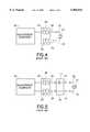
- FIG. 1illustrates the construction of a first embodiment of the present invention.
- FIG. 2illustrates a circuit design for the first embodiment of the present invention.
- FIG. 3illustrates a circuit design for a second embodiment of the present invention.
- FIG. 4illustrates an example of a circuit design of the prior art.
- FIG. 5illustrates an example of a circuit design of prior art.
- FIG. 6illustrates an example of test fixture of the prior art.
- FIG. 2illustrates a circuit design of a first embodiment of the present invention which includes measurement equipment 30, test fixture 20 and a printed circuit board 10.
- the main body of test fixture 20includes contacts 21 for connecting to printed circuit board 10 and measurement terminals 26 for connecting to an oscillator 31 to be tested 31. It is important to understand that contacts 21 are provided separately from measurement terminals 26.
- Printed circuit board 10includes a load capacitance circuit with contacts 12 and a direct coupling circuit (i.e., a short circuit) with contacts 13.
- FIG. 2illustrates the former arrangement wherein load capacitance 11 is inserted into the measurement circuit.
- load capacitance 11is then connected to oscillator 31, via terminals 26.
- Such an arrangementwill hereinafter be referred to as a load capacitance configuration.
- contacts 13 of printed circuit board 10are connected respectively to contacts 21 of test fixture 20.
- thiscan be accomplished by simply reversing the top and bottom surfaces of printed circuit board 10, changing its direction or orientation so that contacts 13 can be connected to contacts 21. In other words, printed circuit board 10 is rotated such that contacts 13 are directly opposite contacts 21.
- switching between a load capacitance configuration and a direct coupling configurationdoes not require oscillator 31 to be disconnected or additional pressing actions. Instead, the present connected contacts (either contacts 12 or 13) of printed circuit board 10 are disconnected from contacts 21 of test fixture 20; printed circuit board 10 is rotated or re-orientated so that the desired contacts face contacts 21; and the desired contact is then connected to contacts 21.
- FIG. 1illustrates an overview of a construction of the circuit diagram of FIG. 2.
- Printed circuit board 10includes two contacts 12 and one contact 13, located on an edge 14. Load capacitance 11 is connected to contacts 12 by a conductor pattern.
- Contacts 21are held with sleeves 22 to provide flexibility in the axial direction. Contacts 21 and sleeves 22 form a unit, commonly referred to as a "pogo-pin". Although not shown in FIG. 1, sleeves 22 are attached to the main body of test fixture 20.
- Guides 23are provided for attaching printed circuit board 10 to main body of test fixture 20. Guides 23 prevent slippage in the direction perpendicular to the direction in which printed circuit board 10 is attached and the printed circuit board 10 from coming apart.
- the guide constructionis not shown in FIG. 1 and will not be described in further detail because it is not pertinent to the present invention.
- printed circuit board 10can be connected to test fixture 20 to provide either a load capacitance configuration or a direct coupling configuration.
- a load capacitancemay be connected to a circuit element to be measured, i.e., oscillator 31, by inserting printed circuit board 10 along guides 23 such that contacts 21 touch contacts 12 (which are coupled to load capacitance 11).
- contacts 21touch contact 13 thereby forming a short circuit between two contacts 21 (i.e., a direct coupling configuration).
- FIG. 1illustrates an example wherein the conductor pattern of printed circuit board 10 forms the contacts of printed circuit board 10
- other contactsmay also be utilized.
- Contact 13may also be split into two contacts, with a conductor pattern connected between the two contacts.
- contacts 12, 13may also be placed on the pattern side.
- the present inventionmay be realized by placing contacts 12 and 13 on different edges respectively, and by changing the direction in which printed circuit board 10 is inserted, or the orientation of printed circuit board 10.
- contacts 12, 13are mounted on the same edge so that only one edge needs to be manually manipulated for attachment or removal.
- a second embodiment of the inventionemploys test fixture that is capable of interconnection with more than one printed circuit board 10.
- the main body of test fixture 20(FIG. 3) includes two sets of contacts 21 which allow two printed circuit boards 10 to be connected on either side of oscillator 31.
- the load capacitancecan thus be inserted on either side of the terminals of oscillator 31, in order to measure oscillator 31 of the surface mounted type.
- the present inventionimproves the operability of the measurement circuit by simplifying the switching operation between a load capacitance configuration and a direct coupling configuration, and making the exchanging of the oscillator to be tested independent of the load capacitance.
- the present inventionalso can be implemented with smaller sized, low cost equipment, as compared to the prior art method that utilizes a switch in order to switch between the load capacitance and direct coupling configurations.
Landscapes
- Physics & Mathematics (AREA)
- General Physics & Mathematics (AREA)
- Measurement Of Resistance Or Impedance (AREA)
- Testing Electric Properties And Detecting Electric Faults (AREA)
- Oscillators With Electromechanical Resonators (AREA)
Abstract
Description
Claims (7)
Applications Claiming Priority (2)
| Application Number | Priority Date | Filing Date | Title |
|---|---|---|---|
| JP8-197201 | 1996-07-26 | ||
| JP8197201AJPH1038945A (en) | 1996-07-26 | 1996-07-26 | Testing instrument for circuit element |
Publications (1)
| Publication Number | Publication Date |
|---|---|
| US5966015Atrue US5966015A (en) | 1999-10-12 |
Family
ID=16370505
Family Applications (1)
| Application Number | Title | Priority Date | Filing Date |
|---|---|---|---|
| US08/891,565Expired - Fee RelatedUS5966015A (en) | 1996-07-26 | 1997-07-11 | Test fixture for circuit component |
Country Status (2)
| Country | Link |
|---|---|
| US (1) | US5966015A (en) |
| JP (1) | JPH1038945A (en) |
Cited By (4)
| Publication number | Priority date | Publication date | Assignee | Title |
|---|---|---|---|---|
| US20040006636A1 (en)* | 2002-04-19 | 2004-01-08 | Oesterreicher Richard T. | Optimized digital media delivery engine |
| CN109490586A (en)* | 2018-11-01 | 2019-03-19 | 北京无线电计量测试研究所 | A kind of π network fixture and test method for quartz crystal parameter test system |
| CN110161340A (en)* | 2019-06-04 | 2019-08-23 | 格力电器(武汉)有限公司 | Discharge device and test system |
| US11470138B2 (en) | 2004-04-30 | 2022-10-11 | DISH Technologies L.L.C. | Apparatus, system, and method for multi-bitrate content streaming |
Citations (6)
| Publication number | Priority date | Publication date | Assignee | Title |
|---|---|---|---|---|
| US3609547A (en)* | 1970-03-27 | 1971-09-28 | Eugene A Slusser | Integrated circuit test system |
| US3763430A (en)* | 1972-01-14 | 1973-10-02 | Burroughs Corp | Circuit testing method and apparatus |
| US4145620A (en)* | 1977-10-05 | 1979-03-20 | Serel Corporation | Modular dynamic burn-in apparatus |
| US4447782A (en)* | 1982-03-17 | 1984-05-08 | Transat Corp. | Apparatus for automatic measurement of equivalent circuit parameters of piezoelectric resonators |
| US4567432A (en)* | 1983-06-09 | 1986-01-28 | Texas Instruments Incorporated | Apparatus for testing integrated circuits |
| US4782289A (en)* | 1986-05-30 | 1988-11-01 | Hilevel Technology, Inc. | Positioning fixture for integrated circuit chip testing board |
- 1996
- 1996-07-26JPJP8197201Apatent/JPH1038945A/enactivePending
- 1997
- 1997-07-11USUS08/891,565patent/US5966015A/ennot_activeExpired - Fee Related
Patent Citations (6)
| Publication number | Priority date | Publication date | Assignee | Title |
|---|---|---|---|---|
| US3609547A (en)* | 1970-03-27 | 1971-09-28 | Eugene A Slusser | Integrated circuit test system |
| US3763430A (en)* | 1972-01-14 | 1973-10-02 | Burroughs Corp | Circuit testing method and apparatus |
| US4145620A (en)* | 1977-10-05 | 1979-03-20 | Serel Corporation | Modular dynamic burn-in apparatus |
| US4447782A (en)* | 1982-03-17 | 1984-05-08 | Transat Corp. | Apparatus for automatic measurement of equivalent circuit parameters of piezoelectric resonators |
| US4567432A (en)* | 1983-06-09 | 1986-01-28 | Texas Instruments Incorporated | Apparatus for testing integrated circuits |
| US4782289A (en)* | 1986-05-30 | 1988-11-01 | Hilevel Technology, Inc. | Positioning fixture for integrated circuit chip testing board |
Cited By (6)
| Publication number | Priority date | Publication date | Assignee | Title |
|---|---|---|---|---|
| US20040006636A1 (en)* | 2002-04-19 | 2004-01-08 | Oesterreicher Richard T. | Optimized digital media delivery engine |
| US11470138B2 (en) | 2004-04-30 | 2022-10-11 | DISH Technologies L.L.C. | Apparatus, system, and method for multi-bitrate content streaming |
| US11677798B2 (en) | 2004-04-30 | 2023-06-13 | DISH Technologies L.L.C. | Apparatus, system, and method for multi-bitrate content streaming |
| US11991234B2 (en) | 2004-04-30 | 2024-05-21 | DISH Technologies L.L.C. | Apparatus, system, and method for multi-bitrate content streaming |
| CN109490586A (en)* | 2018-11-01 | 2019-03-19 | 北京无线电计量测试研究所 | A kind of π network fixture and test method for quartz crystal parameter test system |
| CN110161340A (en)* | 2019-06-04 | 2019-08-23 | 格力电器(武汉)有限公司 | Discharge device and test system |
Also Published As
| Publication number | Publication date |
|---|---|
| JPH1038945A (en) | 1998-02-13 |
Similar Documents
| Publication | Publication Date | Title |
|---|---|---|
| US4746861A (en) | Test fixture for printed circuit board assembly | |
| US6696848B2 (en) | Load board socket adapter and interface method | |
| US4597631A (en) | Printed circuit card hybrid | |
| KR100479136B1 (en) | Generic interface test adapter | |
| US4084869A (en) | Interconnector for integrated circuit package | |
| US5764071A (en) | Method and system for testing an electronic module mounted on a printed circuit board | |
| DE69723284D1 (en) | ANTENNA ADAPTER | |
| AU5790590A (en) | Printed circuit board test system and application thereof to testing printed circuit boards forming digital signal multiplex-demultiplex equipment | |
| US5158483A (en) | Antenna connector and concealed test jack | |
| CA2488832A1 (en) | Multi-socket board for open/short tester | |
| US5966015A (en) | Test fixture for circuit component | |
| JPH10227830A (en) | Test board for ic tester | |
| US5393235A (en) | Telecommunications test adapter | |
| CN108399113A (en) | The plug-in type test device of one seed plate module | |
| CN108535552B (en) | Testing device | |
| CN220231812U (en) | Test structure and circuit board testing arrangement convenient to extend | |
| AU2398800A (en) | Dual-pin probe for testing circuit boards | |
| KR950703739A (en) | Apparatus And Method For Detection Alignment of Contacts In A Multisubstrate Electronic Assembly | |
| JP2519283Y2 (en) | Card Module | |
| KR950016091A (en) | Cable management system with service and user line testing | |
| KR100266230B1 (en) | Apparatus for testing characteristics of smd saw filter | |
| KR100266777B1 (en) | Jig for tuner measurement | |
| CN112217069A (en) | Signal test connecting piece and frock based on VITA74 standard | |
| JP3214526B2 (en) | Inspection equipment for printed wiring boards | |
| JPH10142294A (en) | Semiconductor tester equipment |
Legal Events
| Date | Code | Title | Description |
|---|---|---|---|
| AS | Assignment | Owner name:HEWLETT-PACKARD COMPANY, CALIFORNIA Free format text:ASSIGNMENT OF ASSIGNORS INTEREST;ASSIGNOR:HEWLETT-PACKARD JAPAN, LTD.;REEL/FRAME:008705/0882 Effective date:19970709 | |
| AS | Assignment | Owner name:HEWLETT-PACKARD COMPANY, A DELAWARE CORPORATION, C Free format text:MERGER;ASSIGNOR:HEWLETT-PACKARD COMPANY, A CALIFORNIA CORPORATION;REEL/FRAME:010841/0649 Effective date:19980520 | |
| AS | Assignment | Owner name:AGILENT TECHNOLOGIES INC, CALIFORNIA Free format text:ASSIGNMENT OF ASSIGNORS INTEREST;ASSIGNOR:HEWLETT-PACKARD COMPANY;REEL/FRAME:010977/0540 Effective date:19991101 | |
| FEPP | Fee payment procedure | Free format text:PAYOR NUMBER ASSIGNED (ORIGINAL EVENT CODE: ASPN); ENTITY STATUS OF PATENT OWNER: LARGE ENTITY | |
| FPAY | Fee payment | Year of fee payment:4 | |
| FPAY | Fee payment | Year of fee payment:8 | |
| REMI | Maintenance fee reminder mailed | ||
| LAPS | Lapse for failure to pay maintenance fees | ||
| STCH | Information on status: patent discontinuation | Free format text:PATENT EXPIRED DUE TO NONPAYMENT OF MAINTENANCE FEES UNDER 37 CFR 1.362 | |
| FP | Lapsed due to failure to pay maintenance fee | Effective date:20111012 |