US5965917A - Structure and method of formation of body contacts in SOI MOSFETS to elimate floating body effects - Google Patents
Structure and method of formation of body contacts in SOI MOSFETS to elimate floating body effectsDownload PDFInfo
- Publication number
- US5965917A US5965917AUS09/225,248US22524899AUS5965917AUS 5965917 AUS5965917 AUS 5965917AUS 22524899 AUS22524899 AUS 22524899AUS 5965917 AUS5965917 AUS 5965917A
- Authority
- US
- United States
- Prior art keywords
- region
- silicon
- layer
- doped
- insulator
- Prior art date
- Legal status (The legal status is an assumption and is not a legal conclusion. Google has not performed a legal analysis and makes no representation as to the accuracy of the status listed.)
- Expired - Lifetime
Links
Images


Classifications
- H—ELECTRICITY
- H10—SEMICONDUCTOR DEVICES; ELECTRIC SOLID-STATE DEVICES NOT OTHERWISE PROVIDED FOR
- H10D—INORGANIC ELECTRIC SEMICONDUCTOR DEVICES
- H10D30/00—Field-effect transistors [FET]
- H10D30/01—Manufacture or treatment
- H10D30/021—Manufacture or treatment of FETs having insulated gates [IGFET]
- H10D30/031—Manufacture or treatment of FETs having insulated gates [IGFET] of thin-film transistors [TFT]
- H10D30/0321—Manufacture or treatment of FETs having insulated gates [IGFET] of thin-film transistors [TFT] comprising silicon, e.g. amorphous silicon or polysilicon
- H10D30/0323—Manufacture or treatment of FETs having insulated gates [IGFET] of thin-film transistors [TFT] comprising silicon, e.g. amorphous silicon or polysilicon comprising monocrystalline silicon
- H—ELECTRICITY
- H10—SEMICONDUCTOR DEVICES; ELECTRIC SOLID-STATE DEVICES NOT OTHERWISE PROVIDED FOR
- H10D—INORGANIC ELECTRIC SEMICONDUCTOR DEVICES
- H10D30/00—Field-effect transistors [FET]
- H10D30/60—Insulated-gate field-effect transistors [IGFET]
- H10D30/67—Thin-film transistors [TFT]
- H10D30/6704—Thin-film transistors [TFT] having supplementary regions or layers in the thin films or in the insulated bulk substrates for controlling properties of the device
- H10D30/6708—Thin-film transistors [TFT] having supplementary regions or layers in the thin films or in the insulated bulk substrates for controlling properties of the device for preventing the kink effect or the snapback effect, e.g. discharging the minority carriers of the channel region for preventing bipolar effect
- H10D30/6711—Thin-film transistors [TFT] having supplementary regions or layers in the thin films or in the insulated bulk substrates for controlling properties of the device for preventing the kink effect or the snapback effect, e.g. discharging the minority carriers of the channel region for preventing bipolar effect by using electrodes contacting the supplementary regions or layers
- H—ELECTRICITY
- H10—SEMICONDUCTOR DEVICES; ELECTRIC SOLID-STATE DEVICES NOT OTHERWISE PROVIDED FOR
- H10D—INORGANIC ELECTRIC SEMICONDUCTOR DEVICES
- H10D30/00—Field-effect transistors [FET]
- H10D30/60—Insulated-gate field-effect transistors [IGFET]
- H10D30/67—Thin-film transistors [TFT]
- H10D30/6729—Thin-film transistors [TFT] characterised by the electrodes
Definitions
- the present inventionrelates to silicon-on-insulator devices, and more particularly to silicon-on-insulator devices fabricated to eliminate floating body effects.
- SOI MOSFETsSilicon-on-insulator metal oxide semiconductor field effect transistors
- VLSIvery large scale integration
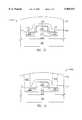
- FIG. 1depicts a SOI MOSFET semiconductor structure 100 of the prior art.
- Structure 100includes insulator 114 positioned over bottom substrate layer 116. Insulator 114 surrounds body region 112. Source region 108 and drain region 110 are positioned within body region 112, and gate electrode 106 is positioned above body region 112. Side wall spacers 122 and 124 surround gate electrode 106. A barrier layer 118 and oxide layer 120 are formed over insulator 114, source region 108, drain region 110, and gate electrode 106. Electrical contacts 102 and 104, source region 108, and drain region 110 are formed through barrier layer 118 and oxide layer 120.
- Body region 112is electrically isolated and therefore its voltage varies with the voltages applied to either source region 108, drain region 110, or gate electrode 106.
- the voltage of body region 112also changes to accommodate the change in applied voltage, but in a different amount of time than it takes the source or drain terminals to achieve the applied voltage.
- the voltage of body region 112varies undesirably because the body region is electrically isolated (so called "floating body effect"). The floating body effect introduces undesirable effects.
- Floating body effectscause, for example, sharp increases in the relationship between drain current and drain voltage (so called “kink effect”), anomalous subthreshold current, transient current overshoot, and early device voltage V DS breakdown.
- the kink effectmay lead to lower device gain, which is undesirable in analog applications.
- Floating body effectsremains a major obstacle to acceptable operation of SOI MOSFET transistors.
- An embodiment of the present inventionincludes a silicon-on-insulator structure including 1) a silicon substrate layer; 2) an insulator layer over the silicon substrate layer; 3) a silicon region over the insulator layer; 4) a body region formed within the silicon region, the body region further includes a first doped region and a second doped region; 5) an isolation region formed in the silicon region that surrounds the body region; and 6) a metal connector that directly contacts a top and side of the first doped region and a side of the body region.
- Another embodiment of the present inventionincludes a method of forming a semiconductor-on-insulator structure in a structure including a bottom substrate layer, middle insulator layer, and top silicon layer, including: 1) forming at least two isolation regions in the silicon layer to the depth of the insulator layer to define a silicon region; 2) doping the silicon region; 3) forming a first and second doped regions in the doped silicon region, the first doped region and the second doped region are not as deep as the silicon region; and 4) forming an electrical contact to directly contact a side of the silicon region and a top and side of the first doped region.
- FIG. 1depicts a SOI MOSFET semiconductor structure 100 of the prior art.
- FIG. 2depicts an SOI N-MOSFET semiconductor structure 200 in accordance with a first embodiment of the present invention.
- FIG. 3depicts a conventional SOI wafer 300 as is well known in the prior art.
- FIG. 4depicts a structure 400 showing silicon region 402 surrounded by isolation region 230.
- FIG. 5depicts a doping of silicon region 402 with ions 502.
- FIG. 6depicts a structure 600 with oxide layer 234.
- FIG. 7depicts a resulting structure 700 with gate region 702.
- FIG. 8depicts a structure 800 with source region 802, drain region 804, and doped gate region 808.
- FIG. 9depicts resulting structure 900 with side wall spacers 224.
- FIG. 10depicts a structure 1000 with source region 208, drain region 210, and gate electrode 206.
- FIG. 11depicts a structure 1100 with silicide covers 226, 222, and 228.
- FIG. 12depicts a structure 1200 with barrier layer 218.
- FIG. 13depicts the resulting structure 1300 with oxide layer 220.
- FIG. 14depicts structure 1400 with openings 1402 and 1404.
- FIG. 2depicts an SOI N-MOSFET semiconductor structure 200 in accordance with a first embodiment of the present invention.
- the structure 200could easily be modified to be a SOI P-MOSFET semiconductor structure.
- a method of fabricating structure 200is described later with respect to a second embodiment of the present invention.
- a conventional n-type substrate layer 216 that is approximately 800 microns thickis covered by a conventional silicon dioxide layer 214 that is approximately 2000 angstroms thick.
- Located above silicon dioxide layer 214are conventional isolation region 230, a conventional body region 212, and electrical contact 202.
- Each isolation region 230is approximately 2000 angstroms thick.
- body region 212is p-type and is approximately 2000 angstroms thick.
- a conventional n+ source region 208 and conventional n+ drain region 210are present within conventional body region 212.
- Source region 208 and drain region 210are not as thick as body region 212.
- Electrical contact 202contacts the top as well as the side of source region 208 and the side of body region 212.
- a suitable material for electrical contact 202is tungsten. Approximately half of the width W of electrical contact 202 extends to contact the side of source region 208 and body region 212.
- oxide layer 234covers a portion of body region 212 between source region 208 and drain region 210.
- oxide layer 234is silicon dioxide and is approximately 15 to 100 angstroms thick.
- a conventional n-type gate electrode 206is positioned above oxide layer 234 between source region 208 and drain region 210.
- Gate electrode 206is approximately 1500 to 2500 angstroms thick.
- Side wall spacers 224cover sides of gate electrode 206.
- Side wall spacers 206are approximately 200 to 2000 angstroms thick and are made of silicon dioxide (SiO 2 ), or silicon nitride (Si 3 N 4 ), or a combination of silicon dioxide and silicon nitride.
- a conventional silicide cover 222covers gate electrode 206.
- conventional silicide covers 226 and 228cover respective source region 208 and drain region 210.
- a suitable material for the silicide coversis a metal silicide such as titanium or cobalt silicide.
- the silicide coversare approximately 200 to 2000 angstroms thick.
- Conventional electrical contact 204contacts silicide cover 228 and extends to the surface of structure 200.
- a suitable material for electrical contact 204is tungsten.
- barrier layer 218covers portions of silicide covers 226 and 228, silicide cover 222, side wall spacers 224, and isolation region 230.
- Barrier layer 218is approximately 300 angstroms thick.
- a suitable material for barrier layer 218is silicon oxi-nitride.
- Oxide layer 220covers barrier layer 218.
- Oxide layer 220is approximately 5000 to 10000 angstroms thick.
- a suitable material for oxide layer 220is silicon dioxide.
- electrical contact 102is in contact with only the top surface of source region 108.
- the voltage of body region 112varies uncontrollably because the body region is electrically isolated.
- a voltage applied to electrical contact 202sets the voltage of body region 212 because electrical contact 202 is directly coupled to body region 212.
- a second embodiment of the present inventionincludes a process to fabricate structure 100 of the first embodiment of the present invention.
- FIG. 3depicts a conventional SOI wafer 300 as is well known in the prior art.
- a suitable silicon waferincludes an upper layer of crystalline silicon 302, a middle layer of silicon dioxide (SiO 2 ) 214, and a lower substrate layer 216.
- Upper layer 302is approximately 2000 angstroms thick
- middle layer 214is approximately 2000 angstroms thick
- substrate layer 216is approximately 800 microns thick.
- a suitable embodiment of SOI wafer 300is available for example from Ibis Technology.
- FIG. 4depicts a resulting structure 400 showing silicon region 402 surrounded by isolation region 230.
- a suitable method to create isolation region 230is a well known shallow trench isolation technique. For example, a dry etch technique may be used to form isolation region 230 to the depth of middle layer 214. Isolation region 230 is then filled with conventional oxides.
- silicon region 402is doped conventionally by ions 502 to become a p-type body region 212.
- FIG. 5depicts a doping of silicon region 402 with ions 502.
- a suitable techniqueis to apply a dose of 1 ⁇ 10 13 p-/cm 2 of boron ions. After doping silicon region 402 becomes body region 212 (not depicted).
- Oxide layer 234has a thickness of 15 to 60 angstroms.
- FIG. 6depicts the resulting structure 600 with oxide layer 234.
- a gate regionis next formed conventionally over oxide layer 234 of structure 600.
- a suitable techniqueis to deposit a layer of amorphous silicon or polysilicon over structure 600 and then apply a dry etch to form gate region 702.
- FIG. 7depicts the resulting structure 700 with gate region 702.
- a suitable thickness for gate region 702is 1500 to 2500 angstroms.
- FIG. 7depicts the resulting structure 800 with source region 802, drain region 804, and doped gate region 808.
- side wall spacersare formed conventionally on the side of doped gate region 808 of structure 800 of FIG. 8.
- a suitable technique to form side wall spacersis to deposit oxide or nitride over the structure 800 of FIG. 8 and then anisotropically etch the resulting structure.
- a suitable width for side wall spacersis 200 to 2000 angstroms.
- FIG. 9depicts resulting structure 900 with side wall spacers 224.
- a conventional deep source region and conventional deep drain regionare formed in the structure 900 of FIG. 9.
- the deep source and drain regionsare formed to a depth above middle layer 214.
- a suitable techniqueis to apply a dose of 1 ⁇ 10 15 n+/cm 2 of ions such as arsenic or boron to the surface of regions 802 and 804 and doped gate region 808.
- An energy levelshould be chosen so that the resulting source and drain junctions are formed above middle layer 214.
- the resulting structureis then annealed at a temperature of 1000° C. for less than 1 minute.
- FIG. 10depicts the resulting structure 1000 with source region 208, drain region 210, and gate electrode 206.
- a silicideis conventionally formed over gate electrode 206, and over source region 208 and drain region 210 of structure 1000 of FIG. 10.
- a suitable techniqueis to deposit a metal such as titanium or cobalt over structure 1000.
- the resulting structureis heated to a temperature of approximately 400 to 500° C. to form a metal silicide.
- the portions of metal outside of gate electrode 206, source region 208, or drain region 210are removed by a conventional etch technique.
- the resulting structureis then heated again to a temperature of 700 to 800° C.
- the thickness of each silicide coveris approximately 200 to 300 angstroms or at least a thickness shallower than the depth of the source or drain junctions.
- FIG. 11depicts a structure 1100 with silicide covers 226, 222, and 228.
- FIG. 12depicts the resulting structure 1200 with barrier layer 218.
- FIG. 13depicts the resulting structure 1300 with oxide layer 220.
- Oxide layeris approximately 5000 to 10000 angstroms thick.
- a suitable material for oxide layer 220is silicon dioxide.
- Opening 1402defines an open space adjacent to the side of body region 212 and source region 208 and above source region 208. Opening 1404 defines a space above drain region 210.
- a suitable technique to form openings 1402 and 1404is a conventional dry etch.
- Openings 1402 and 1404are next filled with an electrically conductive material to provide electrical contacts. Any excess electrically conductive material on the top of oxide layer 220 is then removed. The resulting structure is shown as structure 200 of FIG. 2 with electrical contacts 202 and 204.
- a suitable electrically conductive materialis a metal such as tungsten.
Landscapes
- Thin Film Transistor (AREA)
Abstract
Description
The present invention relates to silicon-on-insulator devices, and more particularly to silicon-on-insulator devices fabricated to eliminate floating body effects.
Silicon-on-insulator (SOI) metal oxide semiconductor field effect transistors (MOSFETs) are well known in the field of semiconductors. SOI MOSFETs have been demonstrated to be superior to bulk silicon MOSFETs in low-power, high-speed very large scale integration (VLSI) applications. The advantages include 1) less junction capacitance so that higher circuit speed can be achieved; 2) better device isolation; and 3) sufficient radiation hardness.
FIG. 1 depicts a SOIMOSFET semiconductor structure 100 of the prior art.Structure 100 includesinsulator 114 positioned overbottom substrate layer 116.Insulator 114surrounds body region 112.Source region 108 anddrain region 110 are positioned withinbody region 112, andgate electrode 106 is positioned abovebody region 112.Side wall spacers surround gate electrode 106. Abarrier layer 118 andoxide layer 120 are formed overinsulator 114,source region 108,drain region 110, andgate electrode 106.Electrical contacts source region 108, anddrain region 110 are formed throughbarrier layer 118 andoxide layer 120.
As shown,electrical contacts respective source region 108 and drainregion 110.Body region 112 is electrically isolated and therefore its voltage varies with the voltages applied to eithersource region 108,drain region 110, orgate electrode 106. When a voltage applied to a source or drain region changes, the voltage ofbody region 112 also changes to accommodate the change in applied voltage, but in a different amount of time than it takes the source or drain terminals to achieve the applied voltage. The voltage ofbody region 112 varies undesirably because the body region is electrically isolated (so called "floating body effect"). The floating body effect introduces undesirable effects.
Floating body effects cause, for example, sharp increases in the relationship between drain current and drain voltage (so called "kink effect"), anomalous subthreshold current, transient current overshoot, and early device voltage VDS breakdown. The kink effect may lead to lower device gain, which is undesirable in analog applications. Floating body effects remains a major obstacle to acceptable operation of SOI MOSFET transistors.
What is needed is an SOI MOSFET semiconductor structure and method of fabricating the SOI MOSFET semiconductor structure which controls the floating body effects.
An embodiment of the present invention includes a silicon-on-insulator structure including 1) a silicon substrate layer; 2) an insulator layer over the silicon substrate layer; 3) a silicon region over the insulator layer; 4) a body region formed within the silicon region, the body region further includes a first doped region and a second doped region; 5) an isolation region formed in the silicon region that surrounds the body region; and 6) a metal connector that directly contacts a top and side of the first doped region and a side of the body region.
Another embodiment of the present invention includes a method of forming a semiconductor-on-insulator structure in a structure including a bottom substrate layer, middle insulator layer, and top silicon layer, including: 1) forming at least two isolation regions in the silicon layer to the depth of the insulator layer to define a silicon region; 2) doping the silicon region; 3) forming a first and second doped regions in the doped silicon region, the first doped region and the second doped region are not as deep as the silicon region; and 4) forming an electrical contact to directly contact a side of the silicon region and a top and side of the first doped region.
The present invention will be more fully understood in light of the following detailed description taken together with the accompanying drawings.
FIG. 1 depicts a SOIMOSFET semiconductor structure 100 of the prior art.
FIG. 2 depicts an SOI N-MOSFET semiconductor structure 200 in accordance with a first embodiment of the present invention.
FIG. 3 depicts aconventional SOI wafer 300 as is well known in the prior art.
FIG. 4 depicts astructure 400 showingsilicon region 402 surrounded byisolation region 230.
FIG. 5 depicts a doping ofsilicon region 402 withions 502.
FIG. 6 depicts astructure 600 withoxide layer 234.
FIG. 7 depicts a resultingstructure 700 withgate region 702.
FIG. 8 depicts astructure 800 withsource region 802, drainregion 804, and dopedgate region 808.
FIG. 9 depicts resultingstructure 900 withside wall spacers 224.
FIG. 10 depicts astructure 1000 withsource region 208,drain region 210, andgate electrode 206.
FIG. 11 depicts astructure 1100 with silicide covers 226, 222, and 228.
FIG. 12 depicts astructure 1200 withbarrier layer 218.
FIG. 13 depicts the resultingstructure 1300 withoxide layer 220.
FIG. 14 depictsstructure 1400 withopenings
Note that use of the same reference numbers in different figures indicates the same or like elements.
FIG. 2 depicts an SOI N-MOSFET semiconductor structure 200 in accordance with a first embodiment of the present invention. Thestructure 200 could easily be modified to be a SOI P-MOSFET semiconductor structure. A method of fabricatingstructure 200 is described later with respect to a second embodiment of the present invention.
A conventional n-type substrate layer 216 that is approximately 800 microns thick is covered by a conventionalsilicon dioxide layer 214 that is approximately 2000 angstroms thick. Located abovesilicon dioxide layer 214 areconventional isolation region 230, aconventional body region 212, andelectrical contact 202. Eachisolation region 230 is approximately 2000 angstroms thick. In this embodiment,body region 212 is p-type and is approximately 2000 angstroms thick.
A conventionaln+ source region 208 and conventionaln+ drain region 210 are present withinconventional body region 212.Source region 208 and drainregion 210 are not as thick asbody region 212.Electrical contact 202 contacts the top as well as the side ofsource region 208 and the side ofbody region 212. A suitable material forelectrical contact 202 is tungsten. Approximately half of the width W ofelectrical contact 202 extends to contact the side ofsource region 208 andbody region 212.
A conventional n-type gate electrode 206 is positioned aboveoxide layer 234 betweensource region 208 anddrain region 210.Gate electrode 206 is approximately 1500 to 2500 angstroms thick.Side wall spacers 224 cover sides ofgate electrode 206.Side wall spacers 206 are approximately 200 to 2000 angstroms thick and are made of silicon dioxide (SiO2), or silicon nitride (Si3 N4), or a combination of silicon dioxide and silicon nitride.
Aconventional silicide cover 222 coversgate electrode 206. Similarly, conventional silicide covers 226 and 228 coverrespective source region 208 and drainregion 210. A suitable material for the silicide covers is a metal silicide such as titanium or cobalt silicide. The silicide covers are approximately 200 to 2000 angstroms thick.
Conventionalelectrical contact 204contacts silicide cover 228 and extends to the surface ofstructure 200. A suitable material forelectrical contact 204 is tungsten.
In the prior art, as shown in FIG. 1,electrical contact 102 is in contact with only the top surface ofsource region 108. In the prior art, the voltage ofbody region 112 varies uncontrollably because the body region is electrically isolated. In the first embodiment of the present invention, a voltage applied toelectrical contact 202 sets the voltage ofbody region 212 becauseelectrical contact 202 is directly coupled tobody region 212.
A second embodiment of the present invention includes a process to fabricatestructure 100 of the first embodiment of the present invention. FIG. 3 depicts aconventional SOI wafer 300 as is well known in the prior art. A suitable silicon wafer includes an upper layer ofcrystalline silicon 302, a middle layer of silicon dioxide (SiO2) 214, and alower substrate layer 216.Upper layer 302 is approximately 2000 angstroms thick,middle layer 214 is approximately 2000 angstroms thick, andsubstrate layer 216 is approximately 800 microns thick. A suitable embodiment ofSOI wafer 300 is available for example from Ibis Technology.
Next, two conventional isolation regions are formed inupper layer 302. Isolation regions are formed to the depth ofmiddle layer 214 to isolate a silicon region. FIG. 4 depicts a resultingstructure 400 showingsilicon region 402 surrounded byisolation region 230. A suitable method to createisolation region 230 is a well known shallow trench isolation technique. For example, a dry etch technique may be used to formisolation region 230 to the depth ofmiddle layer 214.Isolation region 230 is then filled with conventional oxides.
Next,silicon region 402 is doped conventionally byions 502 to become a p-type body region 212. FIG. 5 depicts a doping ofsilicon region 402 withions 502. A suitable technique is to apply a dose of 1×10¹³ p-/cm2 of boron ions. After dopingsilicon region 402 becomes body region 212 (not depicted).
Next, an oxide layer is formed conventionally overbody region 212 ofstructure 500 by a conventional thermal oxidation technique.Oxide layer 234 has a thickness of 15 to 60 angstroms. FIG. 6 depicts the resultingstructure 600 withoxide layer 234.
A gate region is next formed conventionally overoxide layer 234 ofstructure 600. A suitable technique is to deposit a layer of amorphous silicon or polysilicon overstructure 600 and then apply a dry etch to formgate region 702. FIG. 7 depicts the resultingstructure 700 withgate region 702. A suitable thickness forgate region 702 is 1500 to 2500 angstroms.
Next, conventional shallow source and drain regions are formed in thestructure 700 of FIG. 7 andgate region 702 is doped. A suitable technique is to implant the top of regions shown as 710 and 712 andgate electrode 702 of FIG. 7 each with 1×10¹⁴ n+/cm2 of arsenic ions for example. FIG. 8 depicts the resultingstructure 800 withsource region 802,drain region 804, and dopedgate region 808.
Next, side wall spacers are formed conventionally on the side of dopedgate region 808 ofstructure 800 of FIG. 8. A suitable technique to form side wall spacers is to deposit oxide or nitride over thestructure 800 of FIG. 8 and then anisotropically etch the resulting structure. A suitable width for side wall spacers is 200 to 2000 angstroms. FIG. 9 depicts resultingstructure 900 withside wall spacers 224.
Next a conventional deep source region and conventional deep drain region are formed in thestructure 900 of FIG. 9. The deep source and drain regions are formed to a depth abovemiddle layer 214. A suitable technique is to apply a dose of 1×10¹⁵ n+/cm2 of ions such as arsenic or boron to the surface ofregions gate region 808. An energy level should be chosen so that the resulting source and drain junctions are formed abovemiddle layer 214. The resulting structure is then annealed at a temperature of 1000° C. for less than 1 minute. FIG. 10 depicts the resultingstructure 1000 withsource region 208,drain region 210, andgate electrode 206.
Next a silicide is conventionally formed overgate electrode 206, and oversource region 208 and drainregion 210 ofstructure 1000 of FIG. 10. A suitable technique is to deposit a metal such as titanium or cobalt overstructure 1000. Then the resulting structure is heated to a temperature of approximately 400 to 500° C. to form a metal silicide. The portions of metal outside ofgate electrode 206,source region 208, or drainregion 210 are removed by a conventional etch technique. The resulting structure is then heated again to a temperature of 700 to 800° C. The thickness of each silicide cover is approximately 200 to 300 angstroms or at least a thickness shallower than the depth of the source or drain junctions. FIG. 11 depicts astructure 1100 with silicide covers 226, 222, and 228.
Next a conventional barrier layer is deposited over thestructure 1100 of FIG. 11. A suitable technique is to apply a silicon oxi-nitride layer overstructure 1100. A suitable thickness of the barrier layer is approximately 300 angstroms. FIG. 12 depicts the resultingstructure 1200 withbarrier layer 218.
Next a conventional oxide layer is applied over thestructure 1200 of FIG. 12. FIG. 13 depicts the resultingstructure 1300 withoxide layer 220. Oxide layer is approximately 5000 to 10000 angstroms thick. A suitable material foroxide layer 220 is silicon dioxide.
The above-described embodiments of the present invention are illustrative and not limiting. It will thus be obvious to those skilled in the art that various changes and modifications may be made without departing from this invention in its broader aspects. For example,electrical contact 204 could be coupled to the top and side ofdrain region 210 and the side ofbody region 212 andelectrical contact 202 is coupled to the top ofsource region 208. Further the dose quantities and thicknesses provided are merely illustrative and can be varied. Therefore, the appended claims encompass all such changes and modifications as fall within the true spirit and scope of this invention.
Claims (9)
1. A silicon-on-insulator structure comprising:
a silicon substrate layer;
an insulator layer over said silicon substrate layer;
a silicon region over said insulator layer;
a body region formed within said silicon region, wherein said body region further includes a first doped region and a second doped region;
an isolation region formed in said silicon region that surrounds said body region; and
a metal connector that directly contacts a top and side of said first doped region and a side of said body region.
2. The silicon-on-insulator structure of claim 1 wherein said first doped region comprises a source region.
3. The silicon-on-insulator structure of claim 1 wherein said first doped region comprises a drain region.
4. The silicon-on-insulator structure of claim 1 wherein bottom sides of said first and second doped region are not in contact with said insulator layer.
5. A method of forming a semiconductor-on-insulator structure in a structure including a bottom substrate layer, middle insulator layer, and top silicon layer, comprising:
forming at least two isolation regions in said silicon layer to the depth of said insulator layer to define a silicon region;
doping said silicon region;
forming a first and second doped regions in said doped silicon region, wherein said first doped region and said second doped region are not as deep as said silicon region; and
forming an electrical contact to directly contact a side of said silicon region and a top and side of said first doped region.
6. The method of claim 5 wherein said doping further includes depositing p-type ions.
7. The method of claim 5 wherein said forming a first and second doped regions further includes applying n+ ions.
8. The method of claim 5 wherein said doping further includes depositing n-type ions.
9. The method of claim 5 wherein said forming a first and second doped regions further includes applying p+ ions.
Priority Applications (1)
| Application Number | Priority Date | Filing Date | Title |
|---|---|---|---|
| US09/225,248US5965917A (en) | 1999-01-04 | 1999-01-04 | Structure and method of formation of body contacts in SOI MOSFETS to elimate floating body effects |
Applications Claiming Priority (1)
| Application Number | Priority Date | Filing Date | Title |
|---|---|---|---|
| US09/225,248US5965917A (en) | 1999-01-04 | 1999-01-04 | Structure and method of formation of body contacts in SOI MOSFETS to elimate floating body effects |
Publications (1)
| Publication Number | Publication Date |
|---|---|
| US5965917Atrue US5965917A (en) | 1999-10-12 |
Family
ID=22844147
Family Applications (1)
| Application Number | Title | Priority Date | Filing Date |
|---|---|---|---|
| US09/225,248Expired - LifetimeUS5965917A (en) | 1999-01-04 | 1999-01-04 | Structure and method of formation of body contacts in SOI MOSFETS to elimate floating body effects |
Country Status (1)
| Country | Link |
|---|---|
| US (1) | US5965917A (en) |
Cited By (42)
| Publication number | Priority date | Publication date | Assignee | Title |
|---|---|---|---|---|
| US6218248B1 (en)* | 1998-04-02 | 2001-04-17 | Hyundai Electronics Industries Co., Ltd. | Semiconductor device and method for fabricating the same |
| US20020009856A1 (en)* | 1999-06-29 | 2002-01-24 | Jun Kanamori | Method of fabricating a semiconductor device with self- aligned silicide areas formed using a supplemental silicon overlayer |
| US6376336B1 (en) | 2001-02-01 | 2002-04-23 | Advanced Micro Devices, Inc. | Frontside SOI gettering with phosphorus doping |
| US6388334B1 (en)* | 1999-07-27 | 2002-05-14 | Advanced Micro Devices, Inc. | System and method for circuit rebuilding via backside access |
| US6432777B1 (en)* | 2001-06-06 | 2002-08-13 | International Business Machines Corporation | Method for increasing the effective well doping in a MOSFET as the gate length decreases |
| US6437405B2 (en) | 2000-03-30 | 2002-08-20 | Samsung Electronics Co., Ltd. | Silicon-on-insulator (SOI) substrate, method for fabricating SOI substrate and SOI MOSFET using the SOI substrate |
| US6441435B1 (en) | 2001-01-31 | 2002-08-27 | Advanced Micro Devices, Inc. | SOI device with wrap-around contact to underside of body, and method of making |
| US6444534B1 (en) | 2001-01-30 | 2002-09-03 | Advanced Micro Devices, Inc. | SOI semiconductor device opening implantation gettering method |
| US6452250B1 (en) | 2000-01-20 | 2002-09-17 | Advanced Micro Devices, Inc. | Stacked integrated circuit and capacitor structure containing via structures |
| US6462379B2 (en)* | 1998-05-22 | 2002-10-08 | Sharp Kabushiki Kaisha | SOI semiconductor device and method for manufacturing the same |
| US6465847B1 (en)* | 2001-06-11 | 2002-10-15 | Advanced Micro Devices, Inc. | Semiconductor-on-insulator (SOI) device with hyperabrupt source/drain junctions |
| US6514809B1 (en)* | 2000-11-03 | 2003-02-04 | Advanced Micro Devices, Inc. | SOI field effect transistors with body contacts formed by selective etch and fill |
| US6573566B2 (en)* | 2001-07-09 | 2003-06-03 | United Microelectronics Corp. | Low-voltage-triggered SOI-SCR device and associated ESD protection circuit |
| US6642579B2 (en)* | 2001-08-28 | 2003-11-04 | International Business Machines Corporation | Method of reducing the extrinsic body resistance in a silicon-on-insulator body contacted MOSFET |
| US6670259B1 (en) | 2001-02-21 | 2003-12-30 | Advanced Micro Devices, Inc. | Inert atom implantation method for SOI gettering |
| US20040007744A1 (en)* | 2002-07-12 | 2004-01-15 | Samsung Electronics Co., Ltd. | Semiconductor device having a merged region and method of fabrication |
| US20040121599A1 (en)* | 2002-12-23 | 2004-06-24 | Massud Aminpur | Simultaneous formation of device and backside contacts on wafers having a buried insulator layer |
| US20050012087A1 (en)* | 2003-07-15 | 2005-01-20 | Yi-Ming Sheu | Self-aligned MOSFET having an oxide region below the channel |
| US20050035470A1 (en)* | 2003-08-12 | 2005-02-17 | Chih-Hsin Ko | Strained channel complementary field-effect transistors and methods of manufacture |
| US20050035410A1 (en)* | 2003-08-15 | 2005-02-17 | Yee-Chia Yeo | Semiconductor diode with reduced leakage |
| US20050093067A1 (en)* | 2003-04-30 | 2005-05-05 | Yee-Chia Yeo | Semiconductor-on-insulator chip incorporating strained-channel partially-depleted, fully-depleted, and multiple-gate transistors |
| US20050208717A1 (en)* | 2003-07-25 | 2005-09-22 | Yee-Chia Yeo | Capacitor with enhanced performance and method of manufacture |
| US6958264B1 (en)* | 2001-04-03 | 2005-10-25 | Advanced Micro Devices, Inc. | Scribe lane for gettering of contaminants on SOI wafers and gettering method |
| US20060049467A1 (en)* | 2004-09-09 | 2006-03-09 | Hoon Lim | Body-tied-to-source MOSFETs with asymmetrical source and drain regions and methods of fabricating the same |
| US20060226487A1 (en)* | 2003-08-18 | 2006-10-12 | Yee-Chia Yeo | Resistor with reduced leakage |
| US20070048925A1 (en)* | 2005-08-24 | 2007-03-01 | International Business Machines Corporation | Body-Contacted Silicon on Insulation (SOI) field effect transistors |
| US20070105326A1 (en)* | 2005-11-09 | 2007-05-10 | International Business Machines Corporation | Rotated field effect transistors and method of manufacture |
| US20070164443A1 (en)* | 2005-09-29 | 2007-07-19 | Atmel Germany Gmbh | Semiconductor array and method for manufacturing a semiconductor array |
| US20080237712A1 (en)* | 2007-03-30 | 2008-10-02 | Andy Wei | Soi transistor having drain and source regions of reduced length and a stressed dielectric material adjacent thereto |
| US7646068B2 (en) | 2003-08-15 | 2010-01-12 | Taiwan Semiconductor Manufacturing Company, Ltd. | Structure and method of a strained channel transistor and a second semiconductor component in an integrated circuit |
| US20100032759A1 (en)* | 2008-08-11 | 2010-02-11 | International Business Machines Corporation | self-aligned soi schottky body tie employing sidewall silicidation |
| CN101183683B (en)* | 2006-11-16 | 2010-06-16 | 国际商业机器公司 | Methods and structures for reducing floating body effects in MOSFET devices |
| US7745279B2 (en) | 2003-07-25 | 2010-06-29 | Taiwan Semiconductor Manufacturing Company, Ltd. | Capacitor that includes high permittivity capacitor dielectric |
| US7808051B2 (en) | 2008-09-29 | 2010-10-05 | Taiwan Semiconductor Manufacturing Company, Ltd. | Standard cell without OD space effect in Y-direction |
| US7867860B2 (en) | 2003-07-25 | 2011-01-11 | Taiwan Semiconductor Manufacturing Company, Ltd. | Strained channel transistor formation |
| US7888201B2 (en) | 2003-11-04 | 2011-02-15 | Taiwan Semiconductor Manufacturing Company, Ltd. | Semiconductor-on-insulator SRAM configured using partially-depleted and fully-depleted transistors |
| US7943961B2 (en) | 2008-03-13 | 2011-05-17 | Taiwan Semiconductor Manufacturing Company, Ltd. | Strain bars in stressed layers of MOS devices |
| US20110215415A1 (en)* | 2007-04-30 | 2011-09-08 | Globalfoundries Inc. | Technique for Enhancing Transistor Performance by Transistor Specific Contact Design |
| US8558278B2 (en) | 2007-01-16 | 2013-10-15 | Taiwan Semiconductor Manufacturing Company, Ltd. | Strained transistor with optimized drive current and method of forming |
| US9177968B1 (en) | 2014-09-19 | 2015-11-03 | Silanna Semiconductor U.S.A., Inc. | Schottky clamped radio frequency switch |
| EP3886176A1 (en)* | 2020-03-26 | 2021-09-29 | INTEL Corporation | Device contact sizing in integrated circuit structures |
| US20220051905A1 (en)* | 2020-08-12 | 2022-02-17 | Tokyo Electron Limited | Formation of low-temperature and high-temperature in-situ doped source and drain epitaxy using selective heating for wrap-around contact and vertically stacked device architectures |
Citations (7)
| Publication number | Priority date | Publication date | Assignee | Title |
|---|---|---|---|---|
| US5489792A (en)* | 1994-04-07 | 1996-02-06 | Regents Of The University Of California | Silicon-on-insulator transistors having improved current characteristics and reduced electrostatic discharge susceptibility |
| US5543636A (en)* | 1984-05-18 | 1996-08-06 | Semiconductor Energy Laboratory Co., Ltd. | Insulated gate field effect transistor |
| US5596215A (en)* | 1995-06-08 | 1997-01-21 | Taiwan Semiconductor Manufacturing Company | Method to improve buried contact resistance |
| US5674760A (en)* | 1996-02-26 | 1997-10-07 | United Microelectronics Corporation | Method of forming isolation regions in a MOS transistor device |
| US5696386A (en)* | 1993-02-10 | 1997-12-09 | Semiconductor Energy Laboratory Co. Ltd. | Semiconductor device |
| US5742088A (en)* | 1996-04-22 | 1998-04-21 | Chartered Semiconductor Manufacturing Pte Ltd. | Process having high tolerance to buried contact mask misalignment by using a PSG spacer |
| US5796126A (en)* | 1995-06-14 | 1998-08-18 | Samsung Electronics Co., Ltd. | Hybrid schottky injection field effect transistor |
- 1999
- 1999-01-04USUS09/225,248patent/US5965917A/ennot_activeExpired - Lifetime
Patent Citations (7)
| Publication number | Priority date | Publication date | Assignee | Title |
|---|---|---|---|---|
| US5543636A (en)* | 1984-05-18 | 1996-08-06 | Semiconductor Energy Laboratory Co., Ltd. | Insulated gate field effect transistor |
| US5696386A (en)* | 1993-02-10 | 1997-12-09 | Semiconductor Energy Laboratory Co. Ltd. | Semiconductor device |
| US5489792A (en)* | 1994-04-07 | 1996-02-06 | Regents Of The University Of California | Silicon-on-insulator transistors having improved current characteristics and reduced electrostatic discharge susceptibility |
| US5596215A (en)* | 1995-06-08 | 1997-01-21 | Taiwan Semiconductor Manufacturing Company | Method to improve buried contact resistance |
| US5796126A (en)* | 1995-06-14 | 1998-08-18 | Samsung Electronics Co., Ltd. | Hybrid schottky injection field effect transistor |
| US5674760A (en)* | 1996-02-26 | 1997-10-07 | United Microelectronics Corporation | Method of forming isolation regions in a MOS transistor device |
| US5742088A (en)* | 1996-04-22 | 1998-04-21 | Chartered Semiconductor Manufacturing Pte Ltd. | Process having high tolerance to buried contact mask misalignment by using a PSG spacer |
Cited By (66)
| Publication number | Priority date | Publication date | Assignee | Title |
|---|---|---|---|---|
| US6337505B2 (en) | 1998-04-02 | 2002-01-08 | Hyundai Electronics Industries Co., Ltd. | Semiconductor device and method for fabricating the same |
| US6218248B1 (en)* | 1998-04-02 | 2001-04-17 | Hyundai Electronics Industries Co., Ltd. | Semiconductor device and method for fabricating the same |
| US6462379B2 (en)* | 1998-05-22 | 2002-10-08 | Sharp Kabushiki Kaisha | SOI semiconductor device and method for manufacturing the same |
| US20020009856A1 (en)* | 1999-06-29 | 2002-01-24 | Jun Kanamori | Method of fabricating a semiconductor device with self- aligned silicide areas formed using a supplemental silicon overlayer |
| US6828206B2 (en) | 1999-06-29 | 2004-12-07 | Oki Electric Industry Co., Ltd. | Semiconductor device and method for fabricating the same |
| US6433388B2 (en)* | 1999-06-29 | 2002-08-13 | Oki Electric Industry Co., Ltd | Semiconductor device with self-aligned areas formed using a supplemental silicon overlayer |
| US6388334B1 (en)* | 1999-07-27 | 2002-05-14 | Advanced Micro Devices, Inc. | System and method for circuit rebuilding via backside access |
| US6452250B1 (en) | 2000-01-20 | 2002-09-17 | Advanced Micro Devices, Inc. | Stacked integrated circuit and capacitor structure containing via structures |
| US6437405B2 (en) | 2000-03-30 | 2002-08-20 | Samsung Electronics Co., Ltd. | Silicon-on-insulator (SOI) substrate, method for fabricating SOI substrate and SOI MOSFET using the SOI substrate |
| US6514809B1 (en)* | 2000-11-03 | 2003-02-04 | Advanced Micro Devices, Inc. | SOI field effect transistors with body contacts formed by selective etch and fill |
| US6444534B1 (en) | 2001-01-30 | 2002-09-03 | Advanced Micro Devices, Inc. | SOI semiconductor device opening implantation gettering method |
| US6441435B1 (en) | 2001-01-31 | 2002-08-27 | Advanced Micro Devices, Inc. | SOI device with wrap-around contact to underside of body, and method of making |
| US6566176B1 (en) | 2001-01-31 | 2003-05-20 | Advanced Micro Devices, Inc. | SOI device with wrap-around contact to underside of body, and method of making |
| US6376336B1 (en) | 2001-02-01 | 2002-04-23 | Advanced Micro Devices, Inc. | Frontside SOI gettering with phosphorus doping |
| US6670259B1 (en) | 2001-02-21 | 2003-12-30 | Advanced Micro Devices, Inc. | Inert atom implantation method for SOI gettering |
| US6958264B1 (en)* | 2001-04-03 | 2005-10-25 | Advanced Micro Devices, Inc. | Scribe lane for gettering of contaminants on SOI wafers and gettering method |
| US6432777B1 (en)* | 2001-06-06 | 2002-08-13 | International Business Machines Corporation | Method for increasing the effective well doping in a MOSFET as the gate length decreases |
| US6465847B1 (en)* | 2001-06-11 | 2002-10-15 | Advanced Micro Devices, Inc. | Semiconductor-on-insulator (SOI) device with hyperabrupt source/drain junctions |
| US6573566B2 (en)* | 2001-07-09 | 2003-06-03 | United Microelectronics Corp. | Low-voltage-triggered SOI-SCR device and associated ESD protection circuit |
| US6642579B2 (en)* | 2001-08-28 | 2003-11-04 | International Business Machines Corporation | Method of reducing the extrinsic body resistance in a silicon-on-insulator body contacted MOSFET |
| US7112856B2 (en)* | 2002-07-12 | 2006-09-26 | Samsung Electronics Co., Ltd. | Semiconductor device having a merged region and method of fabrication |
| US20040007744A1 (en)* | 2002-07-12 | 2004-01-15 | Samsung Electronics Co., Ltd. | Semiconductor device having a merged region and method of fabrication |
| US20060189088A1 (en)* | 2002-07-12 | 2006-08-24 | Samsung Electronics Co., Ltd. | Semiconductor device having a merged region and method of fabrication |
| US20040121599A1 (en)* | 2002-12-23 | 2004-06-24 | Massud Aminpur | Simultaneous formation of device and backside contacts on wafers having a buried insulator layer |
| US7005380B2 (en) | 2002-12-23 | 2006-02-28 | Advanced Micro Devices, Inc. | Simultaneous formation of device and backside contacts on wafers having a buried insulator layer |
| DE10260616B3 (en)* | 2002-12-23 | 2004-09-02 | Advanced Micro Devices, Inc., Sunnyvale | Process for the simultaneous formation of component contacts and rear-side contacts on wafers with a buried insulator layer |
| US20050093067A1 (en)* | 2003-04-30 | 2005-05-05 | Yee-Chia Yeo | Semiconductor-on-insulator chip incorporating strained-channel partially-depleted, fully-depleted, and multiple-gate transistors |
| US7268024B2 (en)* | 2003-04-30 | 2007-09-11 | Taiwan Semiconductor Manufacturing Company, Ltd. | Semiconductor-on-insulator chip incorporating strained-channel partially-depleted, fully-depleted, and multiple-gate transistors |
| US20050012087A1 (en)* | 2003-07-15 | 2005-01-20 | Yi-Ming Sheu | Self-aligned MOSFET having an oxide region below the channel |
| US7867860B2 (en) | 2003-07-25 | 2011-01-11 | Taiwan Semiconductor Manufacturing Company, Ltd. | Strained channel transistor formation |
| US7745279B2 (en) | 2003-07-25 | 2010-06-29 | Taiwan Semiconductor Manufacturing Company, Ltd. | Capacitor that includes high permittivity capacitor dielectric |
| US20050208717A1 (en)* | 2003-07-25 | 2005-09-22 | Yee-Chia Yeo | Capacitor with enhanced performance and method of manufacture |
| US7354843B2 (en) | 2003-07-25 | 2008-04-08 | Taiwan Semiconductor Manufacturing Company, Ltd. | Method of forming a capacitor that includes forming a bottom electrode in a strained silicon layer |
| US7442967B2 (en) | 2003-08-12 | 2008-10-28 | Taiwan Semiconductor Manufacturing Company, Ltd. | Strained channel complementary field-effect transistors |
| US20060189056A1 (en)* | 2003-08-12 | 2006-08-24 | Chih-Hsin Ko | Strained channel complementary field-effect transistors and methods of manufacture |
| US20050035470A1 (en)* | 2003-08-12 | 2005-02-17 | Chih-Hsin Ko | Strained channel complementary field-effect transistors and methods of manufacture |
| US7101742B2 (en) | 2003-08-12 | 2006-09-05 | Taiwan Semiconductor Manufacturing Company, Ltd. | Strained channel complementary field-effect transistors and methods of manufacture |
| US20050035410A1 (en)* | 2003-08-15 | 2005-02-17 | Yee-Chia Yeo | Semiconductor diode with reduced leakage |
| US7646068B2 (en) | 2003-08-15 | 2010-01-12 | Taiwan Semiconductor Manufacturing Company, Ltd. | Structure and method of a strained channel transistor and a second semiconductor component in an integrated circuit |
| US20060226487A1 (en)* | 2003-08-18 | 2006-10-12 | Yee-Chia Yeo | Resistor with reduced leakage |
| US7888201B2 (en) | 2003-11-04 | 2011-02-15 | Taiwan Semiconductor Manufacturing Company, Ltd. | Semiconductor-on-insulator SRAM configured using partially-depleted and fully-depleted transistors |
| US7432560B2 (en)* | 2004-09-09 | 2008-10-07 | Samsung Electronics Co., Ltd. | Body-tied-to-source MOSFETs with asymmetrical source and drain regions and methods of fabricating the same |
| US20060049467A1 (en)* | 2004-09-09 | 2006-03-09 | Hoon Lim | Body-tied-to-source MOSFETs with asymmetrical source and drain regions and methods of fabricating the same |
| US20070048925A1 (en)* | 2005-08-24 | 2007-03-01 | International Business Machines Corporation | Body-Contacted Silicon on Insulation (SOI) field effect transistors |
| US20070164443A1 (en)* | 2005-09-29 | 2007-07-19 | Atmel Germany Gmbh | Semiconductor array and method for manufacturing a semiconductor array |
| US20090160009A1 (en)* | 2005-09-29 | 2009-06-25 | Atmel Germany Gmbh | Semiconductor array and method for manufacturing a semiconductor array |
| US7795098B1 (en) | 2005-11-09 | 2010-09-14 | International Business Machines Corporation | Rotated field effect transistors and method of manufacture |
| US20070105326A1 (en)* | 2005-11-09 | 2007-05-10 | International Business Machines Corporation | Rotated field effect transistors and method of manufacture |
| US7335563B2 (en) | 2005-11-09 | 2008-02-26 | International Business Machines Corporation | Rotated field effect transistors and method of manufacture |
| CN101183683B (en)* | 2006-11-16 | 2010-06-16 | 国际商业机器公司 | Methods and structures for reducing floating body effects in MOSFET devices |
| US8558278B2 (en) | 2007-01-16 | 2013-10-15 | Taiwan Semiconductor Manufacturing Company, Ltd. | Strained transistor with optimized drive current and method of forming |
| US20080237712A1 (en)* | 2007-03-30 | 2008-10-02 | Andy Wei | Soi transistor having drain and source regions of reduced length and a stressed dielectric material adjacent thereto |
| TWI511286B (en)* | 2007-03-30 | 2015-12-01 | Advanced Micro Devices Inc | SOI transistor with reduced length drain and source regions and adjacent dielectric materials |
| US9450073B2 (en)* | 2007-03-30 | 2016-09-20 | Advanced Micro Devices, Inc. | SOI transistor having drain and source regions of reduced length and a stressed dielectric material adjacent thereto |
| US20110215415A1 (en)* | 2007-04-30 | 2011-09-08 | Globalfoundries Inc. | Technique for Enhancing Transistor Performance by Transistor Specific Contact Design |
| US8541885B2 (en)* | 2007-04-30 | 2013-09-24 | Globalfoundries Inc. | Technique for enhancing transistor performance by transistor specific contact design |
| US7943961B2 (en) | 2008-03-13 | 2011-05-17 | Taiwan Semiconductor Manufacturing Company, Ltd. | Strain bars in stressed layers of MOS devices |
| US8389316B2 (en) | 2008-03-13 | 2013-03-05 | Taiwan Semiconductor Manufacturing Company, Ltd. | Strain bars in stressed layers of MOS devices |
| US20100032759A1 (en)* | 2008-08-11 | 2010-02-11 | International Business Machines Corporation | self-aligned soi schottky body tie employing sidewall silicidation |
| US7808051B2 (en) | 2008-09-29 | 2010-10-05 | Taiwan Semiconductor Manufacturing Company, Ltd. | Standard cell without OD space effect in Y-direction |
| US9177968B1 (en) | 2014-09-19 | 2015-11-03 | Silanna Semiconductor U.S.A., Inc. | Schottky clamped radio frequency switch |
| US9502433B2 (en) | 2014-09-19 | 2016-11-22 | Qualcomm Incorporated | Schottky clamped radio frequency switch |
| EP3886176A1 (en)* | 2020-03-26 | 2021-09-29 | INTEL Corporation | Device contact sizing in integrated circuit structures |
| US20210305370A1 (en)* | 2020-03-26 | 2021-09-30 | Intel Corporation | Device contact sizing in integrated circuit structures |
| US11430866B2 (en)* | 2020-03-26 | 2022-08-30 | Intel Corporation | Device contact sizing in integrated circuit structures |
| US20220051905A1 (en)* | 2020-08-12 | 2022-02-17 | Tokyo Electron Limited | Formation of low-temperature and high-temperature in-situ doped source and drain epitaxy using selective heating for wrap-around contact and vertically stacked device architectures |
Similar Documents
| Publication | Publication Date | Title |
|---|---|---|
| US5965917A (en) | Structure and method of formation of body contacts in SOI MOSFETS to elimate floating body effects | |
| US5962895A (en) | SOI transistor having a self-aligned body contact | |
| US5893745A (en) | Methods of forming semiconductor-on-insulator substrates | |
| US5760442A (en) | Semiconductor device of a silicon on insulator metal-insulator type with a concave feature | |
| KR100366965B1 (en) | Soi cmos body contact through gate, self-aligned to source-drain diffusions | |
| US7344945B1 (en) | Method of manufacturing a drain side gate trench metal-oxide-semiconductor field effect transistor | |
| KR100329055B1 (en) | SOI, MOSFET and its manufacturing method | |
| US6177299B1 (en) | Transistor having substantially isolated body and method of making the same | |
| US7253484B2 (en) | Low-power multiple-channel fully depleted quantum well CMOSFETs | |
| US6294817B1 (en) | Source/drain-on insulator (S/DOI) field effect transistor using oxidized amorphous silicon and method of fabrication | |
| US6506638B1 (en) | Vertical double gate transistor structure | |
| KR100344734B1 (en) | Self-aligned dynamic threshold cmos device | |
| US5599728A (en) | Method of fabricating a self-aligned high speed MOSFET device | |
| KR20030004144A (en) | Semiconductor device and method for manufacturing the same | |
| US6166412A (en) | SOI device with double gate and method for fabricating the same | |
| US6501135B1 (en) | Germanium-on-insulator (GOI) device | |
| US6033231A (en) | Semiconductor device having a pedestal and method of forming | |
| US5191397A (en) | SOI semiconductor device with a wiring electrode contacts a buried conductor and an impurity region | |
| US5877058A (en) | Method of forming an insulated-gate field-effect transistor with metal spacers | |
| US6512244B1 (en) | SOI device with structure for enhancing carrier recombination and method of fabricating same | |
| US7407844B2 (en) | Planar dual gate semiconductor device | |
| US20060068542A1 (en) | Isolation trench perimeter implant for threshold voltage control | |
| KR0155840B1 (en) | MOS transistor and manufacturing method thereof | |
| JPH06177377A (en) | Insulated-gate field-effect transistor | |
| US5808362A (en) | Interconnect structure and method of forming |
Legal Events
| Date | Code | Title | Description |
|---|---|---|---|
| AS | Assignment | Owner name:ADVANCED MICRO DEVICES, INC., CALIFORNIA Free format text:ASSIGNMENT OF ASSIGNORS INTEREST;ASSIGNORS:MASZARA, WITOLD;KRISHNAN, SRINATH;REEL/FRAME:009692/0015 Effective date:19981210 | |
| STCF | Information on status: patent grant | Free format text:PATENTED CASE | |
| FPAY | Fee payment | Year of fee payment:4 | |
| FPAY | Fee payment | Year of fee payment:8 | |
| AS | Assignment | Owner name:GLOBALFOUNDRIES INC., CAYMAN ISLANDS Free format text:AFFIRMATION OF PATENT ASSIGNMENT;ASSIGNOR:ADVANCED MICRO DEVICES, INC.;REEL/FRAME:023119/0083 Effective date:20090630 | |
| FPAY | Fee payment | Year of fee payment:12 | |
| AS | Assignment | Owner name:GLOBALFOUNDRIES U.S. INC., NEW YORK Free format text:RELEASE BY SECURED PARTY;ASSIGNOR:WILMINGTON TRUST, NATIONAL ASSOCIATION;REEL/FRAME:056987/0001 Effective date:20201117 |