US5963801A - Method of forming retrograde well structures and punch-through barriers using low energy implants - Google Patents
Method of forming retrograde well structures and punch-through barriers using low energy implantsDownload PDFInfo
- Publication number
- US5963801A US5963801AUS08/770,109US77010996AUS5963801AUS 5963801 AUS5963801 AUS 5963801AUS 77010996 AUS77010996 AUS 77010996AUS 5963801 AUS5963801 AUS 5963801A
- Authority
- US
- United States
- Prior art keywords
- substrate
- wafer
- well
- implant
- type dopant
- Prior art date
- Legal status (The legal status is an assumption and is not a legal conclusion. Google has not performed a legal analysis and makes no representation as to the accuracy of the status listed.)
- Expired - Lifetime
Links
- 239000007943implantSubstances0.000titleclaimsabstractdescription112
- 230000004888barrier functionEffects0.000titleclaimsabstractdescription23
- 238000000034methodMethods0.000titleclaimsdescription32
- 239000000758substrateSubstances0.000claimsabstractdescription75
- 239000002019doping agentSubstances0.000claimsabstractdescription37
- 238000004519manufacturing processMethods0.000claimsdescription17
- 238000002955isolationMethods0.000claimsdescription11
- 125000004437phosphorous atomChemical group0.000claimsdescription8
- 238000000137annealingMethods0.000claimsdescription7
- 239000004065semiconductorSubstances0.000claimsdescription6
- 238000004140cleaningMethods0.000claimsdescription5
- 229910052796boronInorganic materials0.000description21
- ZOXJGFHDIHLPTG-UHFFFAOYSA-NBoronChemical compound[B]ZOXJGFHDIHLPTG-UHFFFAOYSA-N0.000description20
- OAICVXFJPJFONN-UHFFFAOYSA-NPhosphorusChemical compound[P]OAICVXFJPJFONN-UHFFFAOYSA-N0.000description17
- 229910052698phosphorusInorganic materials0.000description17
- 239000011574phosphorusSubstances0.000description17
- 229910052751metalInorganic materials0.000description11
- 239000002184metalSubstances0.000description11
- 239000000463materialSubstances0.000description7
- 125000004429atomChemical group0.000description5
- 230000000873masking effectEffects0.000description5
- VYPSYNLAJGMNEJ-UHFFFAOYSA-NSilicium dioxideChemical compoundO=[Si]=OVYPSYNLAJGMNEJ-UHFFFAOYSA-N0.000description4
- 230000015556catabolic processEffects0.000description4
- 230000000295complement effectEffects0.000description4
- XUIMIQQOPSSXEZ-UHFFFAOYSA-NSiliconChemical compound[Si]XUIMIQQOPSSXEZ-UHFFFAOYSA-N0.000description3
- 150000004767nitridesChemical class0.000description3
- IJGRMHOSHXDMSA-UHFFFAOYSA-NAtomic nitrogenChemical compoundN#NIJGRMHOSHXDMSA-UHFFFAOYSA-N0.000description2
- VEXZGXHMUGYJMC-UHFFFAOYSA-NHydrochloric acidChemical compoundClVEXZGXHMUGYJMC-UHFFFAOYSA-N0.000description2
- 230000015572biosynthetic processEffects0.000description2
- 239000000969carrierSubstances0.000description2
- 238000007796conventional methodMethods0.000description2
- 238000006731degradation reactionMethods0.000description2
- 238000000151depositionMethods0.000description2
- 238000009792diffusion processMethods0.000description2
- 230000000694effectsEffects0.000description2
- 230000015654memoryEffects0.000description2
- 238000002161passivationMethods0.000description2
- 229920002120photoresistant polymerPolymers0.000description2
- 229910021420polycrystalline siliconInorganic materials0.000description2
- 229920005591polysiliconPolymers0.000description2
- 229910052710siliconInorganic materials0.000description2
- 239000010703siliconSubstances0.000description2
- 239000000377silicon dioxideSubstances0.000description2
- JBRZTFJDHDCESZ-UHFFFAOYSA-NAsGaChemical compound[As]#[Ga]JBRZTFJDHDCESZ-UHFFFAOYSA-N0.000description1
- 229910001218Gallium arsenideInorganic materials0.000description1
- 101001082628Mus musculus H-2 class II histocompatibility antigen gamma chainProteins0.000description1
- 230000005465channelingEffects0.000description1
- 238000005229chemical vapour depositionMethods0.000description1
- 229910052681coesiteInorganic materials0.000description1
- 239000000356contaminantSubstances0.000description1
- 238000011109contaminationMethods0.000description1
- 229910052906cristobaliteInorganic materials0.000description1
- 239000013078crystalSubstances0.000description1
- 230000003247decreasing effectEffects0.000description1
- 230000001419dependent effectEffects0.000description1
- 238000009826distributionMethods0.000description1
- 229910052732germaniumInorganic materials0.000description1
- GNPVGFCGXDBREM-UHFFFAOYSA-Ngermanium atomChemical compound[Ge]GNPVGFCGXDBREM-UHFFFAOYSA-N0.000description1
- 238000010438heat treatmentMethods0.000description1
- 239000002784hot electronSubstances0.000description1
- 239000012535impuritySubstances0.000description1
- 230000005865ionizing radiationEffects0.000description1
- 229910044991metal oxideInorganic materials0.000description1
- 150000004706metal oxidesChemical class0.000description1
- 238000001465metallisationMethods0.000description1
- 239000000203mixtureSubstances0.000description1
- 238000012986modificationMethods0.000description1
- 230000004048modificationEffects0.000description1
- 230000007935neutral effectEffects0.000description1
- 229910052757nitrogenInorganic materials0.000description1
- 238000000059patterningMethods0.000description1
- 238000000206photolithographyMethods0.000description1
- 239000003870refractory metalSubstances0.000description1
- 238000006748scratchingMethods0.000description1
- 230000002393scratching effectEffects0.000description1
- 150000003376siliconChemical class0.000description1
- 235000012239silicon dioxideNutrition0.000description1
- 239000007858starting materialSubstances0.000description1
- 229910052682stishoviteInorganic materials0.000description1
- 229910052905tridymiteInorganic materials0.000description1
Images


Classifications
- H—ELECTRICITY
- H01—ELECTRIC ELEMENTS
- H01L—SEMICONDUCTOR DEVICES NOT COVERED BY CLASS H10
- H01L21/00—Processes or apparatus adapted for the manufacture or treatment of semiconductor or solid state devices or of parts thereof
- H01L21/02—Manufacture or treatment of semiconductor devices or of parts thereof
- H01L21/04—Manufacture or treatment of semiconductor devices or of parts thereof the devices having potential barriers, e.g. a PN junction, depletion layer or carrier concentration layer
- H01L21/18—Manufacture or treatment of semiconductor devices or of parts thereof the devices having potential barriers, e.g. a PN junction, depletion layer or carrier concentration layer the devices having semiconductor bodies comprising elements of Group IV of the Periodic Table or AIIIBV compounds with or without impurities, e.g. doping materials
- H01L21/26—Bombardment with radiation
- H01L21/263—Bombardment with radiation with high-energy radiation
- H01L21/265—Bombardment with radiation with high-energy radiation producing ion implantation
- H01L21/26506—Bombardment with radiation with high-energy radiation producing ion implantation in group IV semiconductors
- H01L21/26513—Bombardment with radiation with high-energy radiation producing ion implantation in group IV semiconductors of electrically active species
- H—ELECTRICITY
- H01—ELECTRIC ELEMENTS
- H01L—SEMICONDUCTOR DEVICES NOT COVERED BY CLASS H10
- H01L21/00—Processes or apparatus adapted for the manufacture or treatment of semiconductor or solid state devices or of parts thereof
- H01L21/02—Manufacture or treatment of semiconductor devices or of parts thereof
- H01L21/04—Manufacture or treatment of semiconductor devices or of parts thereof the devices having potential barriers, e.g. a PN junction, depletion layer or carrier concentration layer
- H01L21/18—Manufacture or treatment of semiconductor devices or of parts thereof the devices having potential barriers, e.g. a PN junction, depletion layer or carrier concentration layer the devices having semiconductor bodies comprising elements of Group IV of the Periodic Table or AIIIBV compounds with or without impurities, e.g. doping materials
- H01L21/26—Bombardment with radiation
- H01L21/263—Bombardment with radiation with high-energy radiation
- H01L21/265—Bombardment with radiation with high-energy radiation producing ion implantation
- H01L21/26586—Bombardment with radiation with high-energy radiation producing ion implantation characterised by the angle between the ion beam and the crystal planes or the main crystal surface
- H—ELECTRICITY
- H10—SEMICONDUCTOR DEVICES; ELECTRIC SOLID-STATE DEVICES NOT OTHERWISE PROVIDED FOR
- H10D—INORGANIC ELECTRIC SEMICONDUCTOR DEVICES
- H10D62/00—Semiconductor bodies, or regions thereof, of devices having potential barriers
- H10D62/10—Shapes, relative sizes or dispositions of the regions of the semiconductor bodies; Shapes of the semiconductor bodies
- H10D62/17—Semiconductor regions connected to electrodes not carrying current to be rectified, amplified or switched, e.g. channel regions
- H10D62/213—Channel regions of field-effect devices
- H10D62/221—Channel regions of field-effect devices of FETs
- H10D62/235—Channel regions of field-effect devices of FETs of IGFETs
- H10D62/314—Channel regions of field-effect devices of FETs of IGFETs having vertical doping variations
- H—ELECTRICITY
- H10—SEMICONDUCTOR DEVICES; ELECTRIC SOLID-STATE DEVICES NOT OTHERWISE PROVIDED FOR
- H10D—INORGANIC ELECTRIC SEMICONDUCTOR DEVICES
- H10D84/00—Integrated devices formed in or on semiconductor substrates that comprise only semiconducting layers, e.g. on Si wafers or on GaAs-on-Si wafers
- H10D84/01—Manufacture or treatment
- H10D84/0123—Integrating together multiple components covered by H10D12/00 or H10D30/00, e.g. integrating multiple IGBTs
- H10D84/0126—Integrating together multiple components covered by H10D12/00 or H10D30/00, e.g. integrating multiple IGBTs the components including insulated gates, e.g. IGFETs
- H10D84/0165—Integrating together multiple components covered by H10D12/00 or H10D30/00, e.g. integrating multiple IGBTs the components including insulated gates, e.g. IGFETs the components including complementary IGFETs, e.g. CMOS devices
- H10D84/0191—Manufacturing their doped wells
- H—ELECTRICITY
- H10—SEMICONDUCTOR DEVICES; ELECTRIC SOLID-STATE DEVICES NOT OTHERWISE PROVIDED FOR
- H10D—INORGANIC ELECTRIC SEMICONDUCTOR DEVICES
- H10D84/00—Integrated devices formed in or on semiconductor substrates that comprise only semiconducting layers, e.g. on Si wafers or on GaAs-on-Si wafers
- H10D84/01—Manufacture or treatment
- H10D84/02—Manufacture or treatment characterised by using material-based technologies
- H10D84/03—Manufacture or treatment characterised by using material-based technologies using Group IV technology, e.g. silicon technology or silicon-carbide [SiC] technology
- H10D84/038—Manufacture or treatment characterised by using material-based technologies using Group IV technology, e.g. silicon technology or silicon-carbide [SiC] technology using silicon technology, e.g. SiGe
Definitions
- the inventionrelates to semiconductor fabrication. More specifically, the invention relates to the fabrication of retrograde well structures in CMOS devices.
- CMOSComplementary Metal Oxide Semiconductor
- CMOSComplementary Metal Oxide Semiconductor
- DRAMSdynamic random access memories
- EPROMSerasable programmable read only memories
- CMOS devicesA major problem with CMOS devices is known as "latch-up.” With the p-channel and n-channel transistors being in close proximity, conditions can arise that allow large currents to flow between the drain of one transistor and the source of the complementary transistor. The large currents, in turn, cause high power dissipation, which can stop the CMOS device from functioning or even destroy the CMOS device.
- Latch-upcan arise from voltage overshoot or undershoot at the terminals of the CMOS device, avalanche breakdown at the well-substrate junction, or device degradation that causes current to be shunted through the device.
- Avalanche breakdowncan result from high voltages at the terminals, ionizing radiation, external voltage transients, or large charge buildups at the substrate-well interface.
- Device degradationcould be caused by punch-through between the substrate region and the source/drain region of the device in the well, or avalanche ionization near the drain due to hot-electron effects.
- Latch-up in a CMOS devicecan be prevented by the use of a retrograde well structure.
- a retrograde well structureis formed by performing deep implants to place the dopant at its desired depths without further diffusion. Resulting is a deep peak concentration below the surface and a negative slope approaching the surface (that is, a decreasing concentration towards the surface). The high concentration of dopants implanted near the well bottom shunts the carriers and prevents latch-up from occurring.
- the deep implants for the n-wellsare made by high energy implanters.
- U.S. Pat. No. 5,404,042suggests an implant energy of 1.5 MeV for the deep implants. Although less energy can be used, the implanter still must be capable of performing implants at energies between 300 keV and 700 keV. Such implanters are commercially available, but they are very expensive.
- Low energy implanterswhich perform implants at energies of 220 keV and less, are also commercially available. They are also far less expensive than high energy implanters. If they could perform the deep implants, their usage would lower the cost of fabricating CMOS devices having retrograde well structures. However, using known techniques, the low energy implanters do not have sufficient energy to implant the dopants at the required depths in the substrate. Consequently, only high energy implanters are used at the present time for forming the retrograde well structures.
- a method of performing a deep implant into a substrate of an MOS devicecomprises the steps of cleaning oxide and other material from a surface of the substrate, the surface being cleaned at a location where the implant will be made; and implanting a dopant directly into the cleaned surface of the substrate.
- the dopantis implanted at a low energy in a direction that is substantially co-aligned with lattice channels in the substrate. After the dopant is implanted, the substrate is annealed.
- the deep implantcan be performed by a low energy implanter.
- a method of fabricating a CMOS device having a pair of n-channel and p-channel transistorscomprises the steps of forming isolation islands in the substrate; and doping a first region for the p-channel transistor.
- the first regionis doped by cleaning a surface of oxides and other material at a location where the p-channel transistor will be formed, and implanting an n-type dopant directly into the cleaned surface of the substrate at a low energy in a direction that is substantially co-aligned with channels in the substrate.
- the methodfurther comprises the steps of doping a second region for the n-channel transistor by performing a blanket implant of a p-type dopant; annealing the substrate; forming gate structures over the first and second regions; forming drain and source regions in the first and second regions; and forming contacts for the source and drain regions.
- a method of fabricating a plurality of CMOS devices on a semiconductor wafer having a ⁇ 100> orientationcomprises the steps of forming isolation islands in the wafer; forming an n-well mask on a surface of the wafer, the surface being exposed through the mask at locations where n-wells are to be formed; cleaning the exposed surface of oxide and other material; and directing an n-type dopant towards the wafer at an energy between 150 keV and 220 keV in a direction that is orthogonal to the surface of the wafer.
- the n-type dopantis implanted deeply below the surface of the wafer.
- the methodfurther comprises the steps of stripping the n-well mask; performing a blanket implant of a p-type dopant; annealing the wafer; forming gate structures on the wafer; forming drain and source regions in the wafer; and forming contacts for the source and drain regions.
- An MOS devicecomprises a substrate having a plurality of channels in its lattice structure; and a retrograde n-well formed in the substrate.
- the retrograde n-wellincludes deeply-implanted concentrations of n-type dopant occupying the channels of the substrate and n-type dopant occupying lattice positions in the lattice structure.
- the devicefurther comprises a p-channel device formed in the n-well.
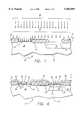
- FIG. 1is an illustration of a CMOS device having its retrograde well being fabricated
- FIG. 2is a illustration of the lattice structure of a silicon substrate and dopant atoms channeling into the substrate, the substrate forming a part of the CMOS device shown in FIG. 1;
- FIG. 3is a first doping profile for the retrograde well of the CMOS vice shown in FIG. 1;
- FIG. 4is a second doping profile for the retrograde well of the CM device shown in FIG. 1;
- FIG. 5is a third doping profile for the retrograde well of the CMOS device shown in FIG. 1;
- FIG. 6is an illustration of the CMOS device after fabrication
- FIG. 7is a flowchart of a method of fabricating the CMOS device shown in FIG. 6;
- FIG. 8is a flowchart of an alternative method of fabricating the CMOS device shown in FIG. 6.
- FIG. 1shows a CMOS device 10 under fabrication.
- the CMOS device 10includes a substrate 12 having a ⁇ 100> crystal axis orientation.
- a p-type substrate 12could be lightly doped with an impurity such as boron in a concentration between 1 ⁇ 10 14 atoms/cm 3 and 5 ⁇ 10 15 atoms/cm 3 , or the p-type substrate could be a heavily doped p + -type substrate upon which a thin, epitaxial layer of lightly doped p-type material is grown.
- Isolation islands 14are formed on the substrate 12 by conventional techniques. For example, a pad-oxide layer is deposited on the substrate 12 and a layer of nitride is deposited on the oxide layer by chemical vapor deposition. Portions of the nitride layer 14 are etched away to expose the oxide layer at the areas where the islands are to be grown. The substrate 12 is heated to temperatures approaching 1000° C., as the exposed oxide is slowly grown into the isolation islands 14. The substrate 12 is heated until the isolation islands 14 reach a desired thickness. Isolation islands 14 for a 0.35 micron CMOS device , for example, might have thicknesses of 5500 angstroms, and they might be spaced apart by 0.4 microns. After the isolation islands 14 are grown, the nitride and underlying pad-oxide are removed from the substrate 12. Remaining between the isolation islands 14 is a bare substrate.
- n-well mask 16is formed on the substrate 12 and patterned to expose the bare surface at the location where an n-well 18 will be formed.
- a p-type transistorwill eventually be formed in the n-well 18.
- the region 20 where an n-type transistor will be formedremains covered by the mask 16.
- the n-well mask 16can be formed from photoresist and patterned by a conventional technique such as photolithography.
- the exposed substrate 12is cleaned of oxide, photoresist and any other matter. A dip in hydrochloric acid does the job.
- a low energy n-well implant 22is made with an n-type dopant such as phosphorus at an energy between 150 keV and 220 keV and in a dose between 5 ⁇ 10 12 phosphorus atoms/cm 2 and 1 ⁇ 10 14 phosphorus atoms/cm 2 .
- the phosphorusis implanted directly into the bare surface of the substrate 12. Additionally, the direction of implant 22 is orthogonal to the surface of the substrate 12, which has the ⁇ 100> orientation.
- the first n-well implant 22can be performed by implanting a dose of approximately 2.5 ⁇ 10 13 phosphorus atoms/cm 2 into the substrate 12 at an energy of 170 keV, 0°.
- Such an implant 22allows the phosphorus to be implanted deeply in the substrate 12.
- the silicon substrate 12has a face-centered cubic lattice structure including "channels" C between silicon atoms A (see FIG. 2).
- the direction of an implant 22is orthogonal to a substrate 12 having a ⁇ 100> orientation, the direction is co-aligned with the channels C. Because the surface of the substrate 12 is bare, the phosphorus atoms are not scattered and enter deeply into the channels before hitting channel walls and lodging between the silicon atoms A.
- the implant anglemust be selected such that the direction of implant is co-aligned with the channels in the substrate. If the implant direction is not aligned with the channels, the phosphorus 22 will not enter deeply into the substrate 12.
- any oxide or other material on the surface of the substrate 12will cause the phosphorus 22 to scatter and enter the channels at incident angles. As a result, the phosphorus 22 will hit the channel walls before entering deeply into the substrate 12. Thus, the surface of the substrate 12 must be cleaned of oxide and other materials prior to the n-well implant 22.
- a punch-through barrier 24is formed in the n-well 18. Punch-through in a p-channel transistor occurs when the depletion region of the well-substrate junction makes contact with the source/drain-well junction. The punch-through barrier 24 prevents such contact from occurring.
- the punch-through barrier 24is formed by performing sequential ("chained") implants 26 at low energies into a shallow region of the n-well 18.
- the punch-through barrier 24extends across the n-well 18.
- the chained implants 26are also made into the bare substrate 12 at an implant angle of 0°.
- the following tablelists three different sequences of implants 26.
- An advantage to the chained implants 26 of groups I and IIIis that the species needs to be changed only once; after the species is changed from phosphorus to boron, only the dose and implant energies of the boron are changed.
- the chained implants 26 of group IIrequire a species change from phosphorus to boron (after the first implant) and back to phosphorus (after the fourth implant).
- FIG. 3shows a doping profile for an n-well 18 resulting from the n-well implant 22 and the chained implants 26 of group I. Doses are represented in atoms/cm 2 , and distance is taken from the surface of the substrate 12.
- FIGS. 4 and 5show doping profiles for n-wells 18 resulting from the n-well implants 22 and the chained implants 26 of groups II and III.
- the region 20 for the n-type transistoris formed.
- the n-well mask 16is stripped and a low-energy blanket implant of a p-type dopant such as boron is performed.
- a blanket implant of approximately 6.8 ⁇ 10 12 boron atoms/cm 2 at 180 keVis made into the substrate 12.
- the substrate 12is annealed to allow the implanted dopants to diffuse to the desired depths.
- the substrate 12is annealed at approximately 900° C. in a neutral ambient such as nitrogen for approximately 30 minutes. This allows the n-well 18, the p-transistor region 20 and the punch-through barrier 24 to be activated at the same time.
- a threshold adjust implant of boron 28is performed.
- a sacrificial oxide layeris grown to a thickness ranging between 200 and 500 angstroms (preferably 300 angstroms).
- a 300 angstrom layer of silicon dioxideis grown by heating the substrate 12 in a steam ambient at 900° C. for approximately 30 minutes.
- the sacrificial oxideprotects the substrate from contamination and keeps the boron implant(s) at a shallow depth.
- One or two implants of boron 28 just below the surface of the substrate 12can provide a correct adjustment of the threshold voltages for both the n-channel and the p-channel transistors.
- the boron 28is implanted through the sacrificial gate oxide in doses between 1 ⁇ 10 12 and 1 ⁇ 10 13 atoms/cm 2 .
- a single implantcan be performed at implant energies between 50 and 100 keV. If two implants are performed to adjust the threshold voltage, the two implants can be performed at lower implant energies. For example, a first implant of boron 28 can be performed at 25 keV and a second implant of boron 28 can be performed at 30 keV.
- the sacrificial oxide layeris stripped and a gate structure is formed.
- a SiO 2 gate oxideis grown, and a layer of polysilicon is deposited on the gate oxide.
- the polysilicon layeris masked and etched into a gate 32, and an n+-type dopant such as phosphorus is implanted into the gate 32.
- the source and drain regions 34 and 36are formed for the n-channel devices.
- An n-source/drain maskis formed on the wafer, exposing the p-wells at locations where the sources and drains of the n-channel transistors are to be formed.
- An n-type dopantis implanted into the p-wells, and an anneal is performed to activate the n-dopant.
- the n-source/drain maskis stripped, and a p-source/drain mask is formed on the wafer, exposing the n-wells at locations where the sources and drains of the p-channel transistors are to be formed.
- a p-type dopantis implanted into the n-wells, and an anneal is performed to activate the p-dopant.
- lightly doped drain regionsare formed to mitigate the effects of hot carriers.
- the LDD regionscan be formed before or after the more heavily doped drain and source regions 34 and 36 are formed.
- a doped oxide layer 38is deposited over the source and drain regions 32 and 34, and contact openings are opened in the oxide layer 38 to expose the source and drain regions 34 and 36.
- a first level of metal contacts 40is formed by depositing a refractory metal layer over the substrate such that the contact openings are filled with the metal.
- a maskis laid over the metal and the metal layer is patterned.
- An annealis performed to diffuse the metal into the drain and source regions 34 and 36 (for shallow junction devices, a diffusion barrier is formed between the metal and the source/drain regions 32 and 34).
- an intermetal dielectricis deposited on the underlying layer, a metal layer is deposited on the intermetal dielectric, and the metal layer is patterned into contacts 40.
- a passivation layer(not shown) is formed over the last level of metal contacts 40.
- the passivation layerprotects the CMOS device 10 from moisture, contaminants and scratching. Bonding pads (not shown) are created in the upper periphery of each die, which allows the die to be connected to a mechanical package.
- CMOS devicesare fabricated simultaneously on a wafer.
- a doped waferis provided as starting material for the CMOS devices (step 100).
- Isolation islands 14 for each deviceare formed on the wafer (step 102) and an n-well mask 16 is formed on the wafer (step 104).
- Exposed through the n-well maskare the regions where the n-wells 18 will be formed.
- the exposed surface of the waferis cleaned of oxide (step 106).
- a low energy implanteris prepared for performing an implant 22 of phosphorus into the wafer (step 108).
- the phosphorusis implanted into the bare surface at an angle that allows the phosphorus to channel deeply into the wafer (step 110).
- the low energy implanteris set up for the chained implants 26 (step 112).
- the implant energy, but not the species or the implant angle,is changed for the first chained implant 26, and the first implant of the chain is performed into the exposed, bare surface of the wafer (step 114).
- the low energy implanteris then prepared for the remaining implants in the chain (step 116).
- the speciesis changed from phosphorus to boron, and the boron is implanted into the bare surface of the wafer. For each remaining implant, the species is not changed; only the implant energies are changed (unless a group II chain is performed, in which case the last implant requires the species to be changed once again to phosphorus).
- the n-well mask 16is stripped, an oxide layer is deposited on the wafer, and a blanket implant of boron is performed to dope the regions 20 for the p-channel transistors (step 118).
- the waferis annealed (step 120).
- the n-wells 18, the regions 20 for the p-channel transistors and the punch-through barriers 24are activated at the same time.
- a threshold voltage adjustmentfollows (step 122).
- a sacrificial layer of oxideis deposited on the wafer, and boron is implanted through the sacrificial oxide to depths just below the surface of the wafer.
- Source and drain regions 34 and 36are then formed, first in the p-doped regions 20, then in the n-wells 18 (step 126). At least one level of metal contacts 40 is formed over the source and drain regions 34 and 36 (step 128).
- FIG. 8shows a different method of fabricating the CMOS device 10. Steps 200-210, leading up to and including the n-well implant 22, are performed in the same manner as the steps 100-110 described above. After the n-well implant 22 is performed, however, the threshold voltage is adjusted. Therefore, after the first n-well implant 22 is made directly into the bare wafer, the n-well mask 16 is stripped, a sacrificial oxide layer is deposited on the wafer (step 212), and the boron is implanted at a dose and energy that are sufficient to adjust the threshold voltages of both the p-channel and n-channel transistors (step 214). The chained implants are then performed through the sacrificial oxide (step 216).
- the sacrificial oxideis stripped (step 218), the p-doped regions 20 are formed by blanket implants (step 220), and the wafer is annealed to activate the n-wells 18, the p-doped regions 20 and the punch-through barriers 24 (step 222).
- Gate structuresare added (step 224), followed by source and drain regions 34 and 36 (step 226) and metal contacts 40 (step 228).
- One advantage of performing the threshold voltage adjustment before the chained implants 26is that time can be saved in setting up the implanter. After the threshold voltage is adjusted, only the species has to be changed (from boron to phosphorus).
- the above-methodsdescribe the formation of punch-through barriers 24 for preventing punch-through from occurring.
- the CMOS device 10does not require a punch-through barrier 24 to be formed.
- pocket implantscan be performed. The pocket implants are performed at high angles to create pocket distributions that protect the drain and source regions 34 and 36.
- the pocket implantsrequire additional masking and other steps to be performed, typically during the formation of the drain and source regions 34 and 36.
- the punch-through barrier 24gives better control than do the pocket implants, and the punch-through barrier 24 can be activated at the same time as the n-wells 18.
- the methods abovecan be easily adapted to make deep p-type implants and create doping profiles having high concentrations of p-type dopants deep in the substrate.
- the blanket implantwould be replaced by an extra masking step (a p-well mask for exposing regions where p-wells are to be formed) and an implant of a p-type dopant such as boron at a 0° angle.
- Energy and dose of the p-well implantwould be selected to place a specific concentration of boron at a desired depth.
- the methodseliminate the need for expensive, high energy implanters to perform the deep implants.
- the methodscan be used for forming retrograde n-wells in CMOS devices, deep concentrations in p-wells and, for that matter, any type of doping profile in a semiconductor substrate.
- the methodsWhen applied to the fabrication of CMOS devices, the methods offer the additional advantages of allowing the punch-through barriers to be activated at the same time as the retrograde wells.
- the methodalso eliminates the need for high angle punch-through implants and the accompanying four wafer rotations that are presently required to form the punch-through barrier. This reduces fabrication time and cost.
- Fabrication time and costare further reduced because the n-well and chained implants are performed in a sequence.
- the sequential implantsdo not require additional masking steps.
- extra timeis required to set up the implanter for chained implants, overall fabrication time is reduced since the masking steps are eliminated.
- the methodis robust in creating well-behaved p-channel devices having stable threshold voltages. Also, the p-channel devices exhibit a reduced leak-through current.
- the substratecan be germanium or gallium arsenide
- the background doping of the substratecan be p-type or n-type.
- the methods and deviceare not limited to the doses, implant energies and implant angles described above. Rather, the doses, implant energies and implant angles are device-dependent, varying upon the desired operational specifications of the device.
- the methodis not limited to the fabrication steps (e.g., depositing, masking, patterning) described above or to the exact order in which they are described. A wide variety of semiconductor fabrication techniques are available. Accordingly, the present invention is not limited to the precise embodiments described hereinabove. Instead, it is defined by the claims that follow.
Landscapes
- Physics & Mathematics (AREA)
- Engineering & Computer Science (AREA)
- High Energy & Nuclear Physics (AREA)
- Health & Medical Sciences (AREA)
- Toxicology (AREA)
- Condensed Matter Physics & Semiconductors (AREA)
- General Physics & Mathematics (AREA)
- Manufacturing & Machinery (AREA)
- Computer Hardware Design (AREA)
- Microelectronics & Electronic Packaging (AREA)
- Power Engineering (AREA)
- Crystallography & Structural Chemistry (AREA)
- Chemical & Material Sciences (AREA)
- Metal-Oxide And Bipolar Metal-Oxide Semiconductor Integrated Circuits (AREA)
Abstract
Description
______________________________________Implant # low energy n-well composition______________________________________I 1 P: 2.3 × 10.sup.13 @ 170 keV 2 B: 4.0 × 10.sup.12 @ 100 keV 3 B: 1.0 × 10.sup.11 @ 70 keV 4 B: 1.0 × 10.sup.11 @ 50 keVII 1 P: 2.5 × 10.sup.13 @ 170 keV 2 B: 4.0 × 10.sup.12 @ 100 keV 3 B: 2.2 × 10.sup.11 @ 70 keV 4 B: 3.0 × 10.sup.11 @ 50 keV 5 P: 4.0 × 10.sup.11 @ 120 keVIII 1 P: 2.5 × 10.sup.13 @ 170 keV 2 B: 4.0 × 10.sup.12 @ 150 keV 3 B: 5.0 × 10.sup.11 @ 80 keV 4 B: 9.0 × 10.sup.11 @ 55 keV______________________________________
Claims (14)
Priority Applications (2)
| Application Number | Priority Date | Filing Date | Title |
|---|---|---|---|
| US08/770,109US5963801A (en) | 1996-12-19 | 1996-12-19 | Method of forming retrograde well structures and punch-through barriers using low energy implants |
| JP9351627AJPH10189475A (en) | 1996-12-19 | 1997-12-19 | Method for forming retrograde well structure and punch-through barrier using low energy implantation |
Applications Claiming Priority (1)
| Application Number | Priority Date | Filing Date | Title |
|---|---|---|---|
| US08/770,109US5963801A (en) | 1996-12-19 | 1996-12-19 | Method of forming retrograde well structures and punch-through barriers using low energy implants |
Publications (1)
| Publication Number | Publication Date |
|---|---|
| US5963801Atrue US5963801A (en) | 1999-10-05 |
Family
ID=25087511
Family Applications (1)
| Application Number | Title | Priority Date | Filing Date |
|---|---|---|---|
| US08/770,109Expired - LifetimeUS5963801A (en) | 1996-12-19 | 1996-12-19 | Method of forming retrograde well structures and punch-through barriers using low energy implants |
Country Status (2)
| Country | Link |
|---|---|
| US (1) | US5963801A (en) |
| JP (1) | JPH10189475A (en) |
Cited By (20)
| Publication number | Priority date | Publication date | Assignee | Title |
|---|---|---|---|---|
| US6255693B1 (en) | 1997-08-11 | 2001-07-03 | Micron Technology, Inc. | Ion implantation with programmable energy, angle, and beam current |
| US6316341B1 (en)* | 2000-02-21 | 2001-11-13 | United Microelectronics Corp. | Method for cell pass transistor design in DRAM process |
| US6410378B2 (en)* | 1997-07-22 | 2002-06-25 | Micron Technonlogy, Inc. | Method of fabrication of semiconductor structures by ion implantation |
| DE10034942B4 (en)* | 2000-07-12 | 2004-08-05 | Infineon Technologies Ag | Method for producing a semiconductor substrate with buried doping |
| US20040155274A1 (en)* | 1999-08-30 | 2004-08-12 | Micron Technology, Inc. | Capacitor structures with recessed hemispherical grain silicon |
| US20050179093A1 (en)* | 2004-02-17 | 2005-08-18 | Silicon Space Technology Corporation | Buried guard ring and radiation hardened isolation structures and fabrication methods |
| US20070141794A1 (en)* | 2005-10-14 | 2007-06-21 | Silicon Space Technology Corporation | Radiation hardened isolation structures and fabrication methods |
| US20080142899A1 (en)* | 2006-08-04 | 2008-06-19 | Silicon Space Technology Corporation | Radiation immunity of integrated circuits using backside die contact and electrically conductive layers |
| US7419863B1 (en)* | 2005-08-29 | 2008-09-02 | National Semiconductor Corporation | Fabrication of semiconductor structure in which complementary field-effect transistors each have hypoabrupt body dopant distribution below at least one source/drain zone |
| US20080308878A1 (en)* | 2005-08-29 | 2008-12-18 | National Semiconductor Corporation | Semiconductor architecture having field-effect transistors especially suitable for analog applications |
| US20080311717A1 (en)* | 2005-08-29 | 2008-12-18 | Constantin Bulucea | Fabrication of semiconductor architecture having field-effect transistors especially suitable for analog applications |
| US7595244B1 (en) | 2000-03-31 | 2009-09-29 | National Semiconductor Corporation | Fabrication of like-polarity insulated-gate field-effect transistors having multiple vertical body dopant concentration maxima and different halo pocket characteristics |
| US20100244130A1 (en)* | 2009-03-27 | 2010-09-30 | National Semiconductor Corporation | Structure and fabrication of field-effect transistor using empty well in combination with source/drain extensions or/and halo pocket |
| US20100244128A1 (en)* | 2009-03-27 | 2010-09-30 | Constantin Bulucea | Configuration and fabrication of semiconductor structure using empty and filled wells |
| US20110097860A1 (en)* | 2009-10-22 | 2011-04-28 | Sanyo Electric Co., Ltd. | Method of manufacturing semiconductor device |
| US8697553B2 (en) | 2008-06-11 | 2014-04-15 | Intevac, Inc | Solar cell fabrication with faceting and ion implantation |
| US8697552B2 (en) | 2009-06-23 | 2014-04-15 | Intevac, Inc. | Method for ion implant using grid assembly |
| US9318332B2 (en) | 2012-12-19 | 2016-04-19 | Intevac, Inc. | Grid for plasma ion implant |
| US9324598B2 (en) | 2011-11-08 | 2016-04-26 | Intevac, Inc. | Substrate processing system and method |
| US10038058B2 (en) | 2016-05-07 | 2018-07-31 | Silicon Space Technology Corporation | FinFET device structure and method for forming same |
Families Citing this family (1)
| Publication number | Priority date | Publication date | Assignee | Title |
|---|---|---|---|---|
| KR100358067B1 (en)* | 1999-12-28 | 2002-10-25 | 주식회사 하이닉스반도체 | Method of manufacturing a flash memory device |
Citations (11)
| Publication number | Priority date | Publication date | Assignee | Title |
|---|---|---|---|---|
| US3925107A (en)* | 1974-11-11 | 1975-12-09 | Ibm | Method of stabilizing mos devices |
| US5384279A (en)* | 1988-09-09 | 1995-01-24 | U.S. Philips Corporation | Method of manufacturing a semiconductor device comprising a silicon body in which semiconductor regions are formed by ion implantations |
| US5399895A (en)* | 1993-03-23 | 1995-03-21 | Mitsubishi Denki Kabushiki Kaisha | Semiconductor device and method of manufacturing thereof |
| US5404042A (en)* | 1990-05-02 | 1995-04-04 | Mitsubishi Denki Kabushiki Kaisha | Semiconductor memory device having a plurality of well regions of different conductivities |
| US5405790A (en)* | 1993-11-23 | 1995-04-11 | Motorola, Inc. | Method of forming a semiconductor structure having MOS, bipolar, and varactor devices |
| US5416038A (en)* | 1994-05-25 | 1995-05-16 | United Microelectronics Corporation | Method for producing semiconductor device with two different threshold voltages |
| US5492845A (en)* | 1993-01-18 | 1996-02-20 | Shin-Etsu Handotai Co., Ltd. | Method of producing MOS devices |
| US5693505A (en)* | 1993-12-24 | 1997-12-02 | Nec Corporation | Method of fabricating a semiconductor device |
| US5693976A (en)* | 1995-03-16 | 1997-12-02 | Taiwan Semiconductor Manufacturing Company Ltd | MOSFET device having denuded zones for forming alignment marks |
| US5747368A (en)* | 1996-10-03 | 1998-05-05 | Mosel Vitelic Inc. | Process for manufacturing CMOS device |
| US5795803A (en)* | 1996-08-29 | 1998-08-18 | Sharp Kabushiki Kaisha | Method for manufacturing a semiconductor device |
- 1996
- 1996-12-19USUS08/770,109patent/US5963801A/ennot_activeExpired - Lifetime
- 1997
- 1997-12-19JPJP9351627Apatent/JPH10189475A/enactivePending
Patent Citations (11)
| Publication number | Priority date | Publication date | Assignee | Title |
|---|---|---|---|---|
| US3925107A (en)* | 1974-11-11 | 1975-12-09 | Ibm | Method of stabilizing mos devices |
| US5384279A (en)* | 1988-09-09 | 1995-01-24 | U.S. Philips Corporation | Method of manufacturing a semiconductor device comprising a silicon body in which semiconductor regions are formed by ion implantations |
| US5404042A (en)* | 1990-05-02 | 1995-04-04 | Mitsubishi Denki Kabushiki Kaisha | Semiconductor memory device having a plurality of well regions of different conductivities |
| US5492845A (en)* | 1993-01-18 | 1996-02-20 | Shin-Etsu Handotai Co., Ltd. | Method of producing MOS devices |
| US5399895A (en)* | 1993-03-23 | 1995-03-21 | Mitsubishi Denki Kabushiki Kaisha | Semiconductor device and method of manufacturing thereof |
| US5405790A (en)* | 1993-11-23 | 1995-04-11 | Motorola, Inc. | Method of forming a semiconductor structure having MOS, bipolar, and varactor devices |
| US5693505A (en)* | 1993-12-24 | 1997-12-02 | Nec Corporation | Method of fabricating a semiconductor device |
| US5416038A (en)* | 1994-05-25 | 1995-05-16 | United Microelectronics Corporation | Method for producing semiconductor device with two different threshold voltages |
| US5693976A (en)* | 1995-03-16 | 1997-12-02 | Taiwan Semiconductor Manufacturing Company Ltd | MOSFET device having denuded zones for forming alignment marks |
| US5795803A (en)* | 1996-08-29 | 1998-08-18 | Sharp Kabushiki Kaisha | Method for manufacturing a semiconductor device |
| US5747368A (en)* | 1996-10-03 | 1998-05-05 | Mosel Vitelic Inc. | Process for manufacturing CMOS device |
Cited By (60)
| Publication number | Priority date | Publication date | Assignee | Title |
|---|---|---|---|---|
| US6410378B2 (en)* | 1997-07-22 | 2002-06-25 | Micron Technonlogy, Inc. | Method of fabrication of semiconductor structures by ion implantation |
| US6794239B2 (en) | 1997-07-22 | 2004-09-21 | Micron Technology, Inc. | Method of fabrication of semiconductor structures by ion implantation |
| US6255693B1 (en) | 1997-08-11 | 2001-07-03 | Micron Technology, Inc. | Ion implantation with programmable energy, angle, and beam current |
| US20040155274A1 (en)* | 1999-08-30 | 2004-08-12 | Micron Technology, Inc. | Capacitor structures with recessed hemispherical grain silicon |
| US6316341B1 (en)* | 2000-02-21 | 2001-11-13 | United Microelectronics Corp. | Method for cell pass transistor design in DRAM process |
| US8129262B1 (en)* | 2000-03-31 | 2012-03-06 | National Semiconductor Corporation | Fabrication of field-effect transistor with vertical body-material dopant profile tailored to alleviate punchthrough and reduce current leakage |
| US7701005B1 (en) | 2000-03-31 | 2010-04-20 | National Semiconductor Corporation | Semiconductor structure in which like-polarity insulated-gate field-effect transistors have multiple vertical body dopant concentration maxima and different halo pocket characteristics |
| US7595244B1 (en) | 2000-03-31 | 2009-09-29 | National Semiconductor Corporation | Fabrication of like-polarity insulated-gate field-effect transistors having multiple vertical body dopant concentration maxima and different halo pocket characteristics |
| US7785971B1 (en) | 2000-03-31 | 2010-08-31 | National Semiconductor Corporation | Fabrication of complementary field-effect transistors with vertical body-material dopant profiles tailored to alleviate punchthrough and reduce current leakage |
| DE10034942B4 (en)* | 2000-07-12 | 2004-08-05 | Infineon Technologies Ag | Method for producing a semiconductor substrate with buried doping |
| US7078325B2 (en) | 2000-07-12 | 2006-07-18 | Infineon Technologies Ag | Process for producing a doped semiconductor substrate |
| US7304354B2 (en) | 2004-02-17 | 2007-12-04 | Silicon Space Technology Corp. | Buried guard ring and radiation hardened isolation structures and fabrication methods |
| US8497195B2 (en) | 2004-02-17 | 2013-07-30 | Silicon Space Technology Corporation | Method for radiation hardening a semiconductor device |
| US20080188045A1 (en)* | 2004-02-17 | 2008-08-07 | Morris Wesley H | Methods for operating and fabricating a semiconductor device having a buried guard ring structure |
| US20080073725A1 (en)* | 2004-02-17 | 2008-03-27 | Morris Wesley H | Buried guard ring structures and fabrication methods |
| US8093145B2 (en) | 2004-02-17 | 2012-01-10 | Silicon Space Technology Corp. | Methods for operating and fabricating a semiconductor device having a buried guard ring structure |
| US8729640B2 (en) | 2004-02-17 | 2014-05-20 | Silicon Space Technology Corporation | Method and structure for radiation hardening a semiconductor device |
| US20060249759A1 (en)* | 2004-02-17 | 2006-11-09 | Morris Wesley H | Buried guard ring and radiation hardened isolation structures and fabrication methods |
| US7629654B2 (en) | 2004-02-17 | 2009-12-08 | Silicon Space Technology Corp. | Buried guard ring structures and fabrication methods |
| US7804138B2 (en) | 2004-02-17 | 2010-09-28 | Silicon Space Technology Corp. | Buried guard ring and radiation hardened isolation structures and fabrication methods |
| US20050179093A1 (en)* | 2004-02-17 | 2005-08-18 | Silicon Space Technology Corporation | Buried guard ring and radiation hardened isolation structures and fabrication methods |
| US8013390B1 (en)* | 2005-08-29 | 2011-09-06 | National Semiconductor Corporation | Semiconductor architecture having field-effect transistors especially suitable for analog applications |
| US8034679B1 (en)* | 2005-08-29 | 2011-10-11 | National Semiconductor Corporation | Fabrication of field-effect transistor having hypoabrupt body dopant distribution below source/drain zone |
| US8309420B1 (en) | 2005-08-29 | 2012-11-13 | National Semiconductor Corporation | Fabrication of semiconductor architecture having field-effect transistors especially suitable for analog applications |
| US7642574B2 (en)* | 2005-08-29 | 2010-01-05 | National Semiconductor Corporation | Semiconductor architecture having field-effect transistors especially suitable for analog applications |
| US8258026B2 (en) | 2005-08-29 | 2012-09-04 | National Semiconductor Corporation | Fabrication of semiconductor architecture having field-effect transistors especially suitable for analog applications |
| US7838369B2 (en) | 2005-08-29 | 2010-11-23 | National Semiconductor Corporation | Fabrication of semiconductor architecture having field-effect transistors especially suitable for analog applications |
| US7838930B1 (en) | 2005-08-29 | 2010-11-23 | National Semiconductor Corporation | Insulated-gate field-effect transistor with hypoabrupt step change in body dopant concentration below source/drain zone |
| US7863681B1 (en)* | 2005-08-29 | 2011-01-04 | National Semiconductor Corporation | Semiconductor structure utilizing empty and filled wells |
| US8148777B1 (en) | 2005-08-29 | 2012-04-03 | National Semiconductor Corporation | Structure and fabrication of insulated-gate field-effect transistor with hypoabrupt change in body dopant concentration below source/drain zone |
| US7972918B1 (en) | 2005-08-29 | 2011-07-05 | National Semiconductor Corporation | Fabrication of semiconductor architecture having field-effect transistors especially suitable for analog applications |
| US20080311717A1 (en)* | 2005-08-29 | 2008-12-18 | Constantin Bulucea | Fabrication of semiconductor architecture having field-effect transistors especially suitable for analog applications |
| US8610207B2 (en) | 2005-08-29 | 2013-12-17 | Texas Instruments Incorporated | Semiconductor architecture having field-effect transistors especially suitable for analog applications |
| US20080308878A1 (en)* | 2005-08-29 | 2008-12-18 | National Semiconductor Corporation | Semiconductor architecture having field-effect transistors especially suitable for analog applications |
| US7419863B1 (en)* | 2005-08-29 | 2008-09-02 | National Semiconductor Corporation | Fabrication of semiconductor structure in which complementary field-effect transistors each have hypoabrupt body dopant distribution below at least one source/drain zone |
| US8252642B2 (en) | 2005-10-14 | 2012-08-28 | Silicon Space Technology Corp. | Fabrication methods for radiation hardened isolation structures |
| US20100267212A1 (en)* | 2005-10-14 | 2010-10-21 | Morris Wesley H | Fabrication methods for radiation hardened isolation structures |
| US8278719B2 (en) | 2005-10-14 | 2012-10-02 | Silicon Space Technology Corp. | Radiation hardened isolation structures and fabrication methods |
| US20070141794A1 (en)* | 2005-10-14 | 2007-06-21 | Silicon Space Technology Corporation | Radiation hardened isolation structures and fabrication methods |
| US20080142899A1 (en)* | 2006-08-04 | 2008-06-19 | Silicon Space Technology Corporation | Radiation immunity of integrated circuits using backside die contact and electrically conductive layers |
| US8697553B2 (en) | 2008-06-11 | 2014-04-15 | Intevac, Inc | Solar cell fabrication with faceting and ion implantation |
| US8871619B2 (en) | 2008-06-11 | 2014-10-28 | Intevac, Inc. | Application specific implant system and method for use in solar cell fabrications |
| US8304835B2 (en) | 2009-03-27 | 2012-11-06 | National Semiconductor Corporation | Configuration and fabrication of semiconductor structure using empty and filled wells |
| US20100244128A1 (en)* | 2009-03-27 | 2010-09-30 | Constantin Bulucea | Configuration and fabrication of semiconductor structure using empty and filled wells |
| US8410549B2 (en) | 2009-03-27 | 2013-04-02 | National Semiconductor Corporation | Structure and fabrication of field-effect transistor using empty well in combination with source/drain extensions or/and halo pocket |
| US20100244130A1 (en)* | 2009-03-27 | 2010-09-30 | National Semiconductor Corporation | Structure and fabrication of field-effect transistor using empty well in combination with source/drain extensions or/and halo pocket |
| US8735980B2 (en) | 2009-03-27 | 2014-05-27 | National Semiconductor Corporation | Configuration and fabrication of semiconductor structure using empty and filled wells |
| US8997688B2 (en) | 2009-06-23 | 2015-04-07 | Intevac, Inc. | Ion implant system having grid assembly |
| US8697552B2 (en) | 2009-06-23 | 2014-04-15 | Intevac, Inc. | Method for ion implant using grid assembly |
| US8749053B2 (en) | 2009-06-23 | 2014-06-10 | Intevac, Inc. | Plasma grid implant system for use in solar cell fabrications |
| US9303314B2 (en) | 2009-06-23 | 2016-04-05 | Intevac, Inc. | Ion implant system having grid assembly |
| US9741894B2 (en) | 2009-06-23 | 2017-08-22 | Intevac, Inc. | Ion implant system having grid assembly |
| US20110097860A1 (en)* | 2009-10-22 | 2011-04-28 | Sanyo Electric Co., Ltd. | Method of manufacturing semiconductor device |
| US8138040B2 (en)* | 2009-10-22 | 2012-03-20 | Semiconductor Components Industries, Llc | Method of manufacturing semiconductor device |
| US9324598B2 (en) | 2011-11-08 | 2016-04-26 | Intevac, Inc. | Substrate processing system and method |
| US9875922B2 (en) | 2011-11-08 | 2018-01-23 | Intevac, Inc. | Substrate processing system and method |
| US9318332B2 (en) | 2012-12-19 | 2016-04-19 | Intevac, Inc. | Grid for plasma ion implant |
| US9583661B2 (en) | 2012-12-19 | 2017-02-28 | Intevac, Inc. | Grid for plasma ion implant |
| US10038058B2 (en) | 2016-05-07 | 2018-07-31 | Silicon Space Technology Corporation | FinFET device structure and method for forming same |
| US10615260B1 (en) | 2016-05-07 | 2020-04-07 | Silicon Space Technology Corporation | Method for forming FinFET device structure |
Also Published As
| Publication number | Publication date |
|---|---|
| JPH10189475A (en) | 1998-07-21 |
Similar Documents
| Publication | Publication Date | Title |
|---|---|---|
| US5963801A (en) | Method of forming retrograde well structures and punch-through barriers using low energy implants | |
| US6794235B1 (en) | Method of manufacturing a semiconductor device having a localized halo implant | |
| US5899732A (en) | Method of implanting silicon through a polysilicon gate for punchthrough control of a semiconductor device | |
| US7064399B2 (en) | Advanced CMOS using super steep retrograde wells | |
| US6548874B1 (en) | Higher voltage transistors for sub micron CMOS processes | |
| US6514810B1 (en) | Buried channel PMOS transistor in dual gate CMOS with reduced masking steps | |
| EP1543546B1 (en) | Process for fabricating an isolated field effect transistor in an epi-less substrate | |
| US5770490A (en) | Method for producing dual work function CMOS device | |
| US5976956A (en) | Method of controlling dopant concentrations using transient-enhanced diffusion prior to gate formation in a device | |
| US6897525B1 (en) | Semiconductor device and method of manufacturing the same | |
| US5943576A (en) | Angled implant to build MOS transistors in contact holes | |
| JP4260905B2 (en) | Method for manufacturing an integrated circuit | |
| US20040110351A1 (en) | Method and structure for reduction of junction capacitance in a semiconductor device and formation of a uniformly lowered threshold voltage device | |
| US4997782A (en) | Fabrication of CMOS integrated devices with reduced gate length and lightly doped drain | |
| KR20030003690A (en) | Semiconductor device and method of fabrication | |
| US4839301A (en) | Blanket CMOS channel stop implant employing a combination of n-channel and p-channel punch-through implants | |
| US20030127694A1 (en) | Higher voltage transistors for sub micron CMOS processes | |
| US6261885B1 (en) | Method for forming integrated circuit gate conductors from dual layers of polysilicon | |
| US6194293B1 (en) | Channel formation after source and drain regions are formed | |
| US6617214B2 (en) | Integrated circuit structure and method therefore | |
| US4987088A (en) | Fabrication of CMOS devices with reduced gate length | |
| US5804497A (en) | Selectively doped channel region for increased IDsat and method for making same | |
| US6692998B2 (en) | Integrated high quality diode | |
| US6180470B1 (en) | FETs having lightly doped drain regions that are shaped with counter and noncounter dorant elements | |
| US5850360A (en) | High-voltage N-channel MOS transistor and associated manufacturing process |
Legal Events
| Date | Code | Title | Description |
|---|---|---|---|
| AS | Assignment | Owner name:LSI LOGIC CORPORATION, CALIFORNIA Free format text:ASSIGNMENT OF ASSIGNORS INTEREST;ASSIGNORS:ARONOWITZ, SHELDON;KHAN, LAIQUE;KIMBALL, JAMES;REEL/FRAME:008497/0018;SIGNING DATES FROM 19970415 TO 19970428 | |
| STCF | Information on status: patent grant | Free format text:PATENTED CASE | |
| FPAY | Fee payment | Year of fee payment:4 | |
| FPAY | Fee payment | Year of fee payment:8 | |
| FEPP | Fee payment procedure | Free format text:PAYOR NUMBER ASSIGNED (ORIGINAL EVENT CODE: ASPN); ENTITY STATUS OF PATENT OWNER: LARGE ENTITY Free format text:PAYER NUMBER DE-ASSIGNED (ORIGINAL EVENT CODE: RMPN); ENTITY STATUS OF PATENT OWNER: LARGE ENTITY | |
| FPAY | Fee payment | Year of fee payment:12 | |
| AS | Assignment | Owner name:DEUTSCHE BANK AG NEW YORK BRANCH, AS COLLATERAL AG Free format text:PATENT SECURITY AGREEMENT;ASSIGNORS:LSI CORPORATION;AGERE SYSTEMS LLC;REEL/FRAME:032856/0031 Effective date:20140506 | |
| AS | Assignment | Owner name:LSI CORPORATION, CALIFORNIA Free format text:CHANGE OF NAME;ASSIGNOR:LSI LOGIC CORPORATION;REEL/FRAME:033102/0270 Effective date:20070406 | |
| AS | Assignment | Owner name:AVAGO TECHNOLOGIES GENERAL IP (SINGAPORE) PTE. LTD Free format text:ASSIGNMENT OF ASSIGNORS INTEREST;ASSIGNOR:LSI CORPORATION;REEL/FRAME:035390/0388 Effective date:20140814 | |
| AS | Assignment | Owner name:LSI CORPORATION, CALIFORNIA Free format text:TERMINATION AND RELEASE OF SECURITY INTEREST IN PATENT RIGHTS (RELEASES RF 032856-0031);ASSIGNOR:DEUTSCHE BANK AG NEW YORK BRANCH, AS COLLATERAL AGENT;REEL/FRAME:037684/0039 Effective date:20160201 Owner name:AGERE SYSTEMS LLC, PENNSYLVANIA Free format text:TERMINATION AND RELEASE OF SECURITY INTEREST IN PATENT RIGHTS (RELEASES RF 032856-0031);ASSIGNOR:DEUTSCHE BANK AG NEW YORK BRANCH, AS COLLATERAL AGENT;REEL/FRAME:037684/0039 Effective date:20160201 | |
| AS | Assignment | Owner name:BANK OF AMERICA, N.A., AS COLLATERAL AGENT, NORTH CAROLINA Free format text:PATENT SECURITY AGREEMENT;ASSIGNOR:AVAGO TECHNOLOGIES GENERAL IP (SINGAPORE) PTE. LTD.;REEL/FRAME:037808/0001 Effective date:20160201 Owner name:BANK OF AMERICA, N.A., AS COLLATERAL AGENT, NORTH Free format text:PATENT SECURITY AGREEMENT;ASSIGNOR:AVAGO TECHNOLOGIES GENERAL IP (SINGAPORE) PTE. LTD.;REEL/FRAME:037808/0001 Effective date:20160201 | |
| AS | Assignment | Owner name:AVAGO TECHNOLOGIES GENERAL IP (SINGAPORE) PTE. LTD., SINGAPORE Free format text:TERMINATION AND RELEASE OF SECURITY INTEREST IN PATENTS;ASSIGNOR:BANK OF AMERICA, N.A., AS COLLATERAL AGENT;REEL/FRAME:041710/0001 Effective date:20170119 Owner name:AVAGO TECHNOLOGIES GENERAL IP (SINGAPORE) PTE. LTD Free format text:TERMINATION AND RELEASE OF SECURITY INTEREST IN PATENTS;ASSIGNOR:BANK OF AMERICA, N.A., AS COLLATERAL AGENT;REEL/FRAME:041710/0001 Effective date:20170119 | |
| AS | Assignment | Owner name:BELL SEMICONDUCTOR, LLC, ILLINOIS Free format text:ASSIGNMENT OF ASSIGNORS INTEREST;ASSIGNORS:AVAGO TECHNOLOGIES GENERAL IP (SINGAPORE) PTE. LTD.;BROADCOM CORPORATION;REEL/FRAME:044886/0608 Effective date:20171208 | |
| AS | Assignment | Owner name:CORTLAND CAPITAL MARKET SERVICES LLC, AS COLLATERA Free format text:SECURITY INTEREST;ASSIGNORS:HILCO PATENT ACQUISITION 56, LLC;BELL SEMICONDUCTOR, LLC;BELL NORTHERN RESEARCH, LLC;REEL/FRAME:045216/0020 Effective date:20180124 | |
| AS | Assignment | Owner name:BELL NORTHERN RESEARCH, LLC, ILLINOIS Free format text:RELEASE BY SECURED PARTY;ASSIGNOR:CORTLAND CAPITAL MARKET SERVICES LLC;REEL/FRAME:059720/0719 Effective date:20220401 Owner name:BELL SEMICONDUCTOR, LLC, ILLINOIS Free format text:RELEASE BY SECURED PARTY;ASSIGNOR:CORTLAND CAPITAL MARKET SERVICES LLC;REEL/FRAME:059720/0719 Effective date:20220401 Owner name:HILCO PATENT ACQUISITION 56, LLC, ILLINOIS Free format text:RELEASE BY SECURED PARTY;ASSIGNOR:CORTLAND CAPITAL MARKET SERVICES LLC;REEL/FRAME:059720/0719 Effective date:20220401 |