US5963057A - Chip level bias for buffers driving voltages greater than transistor tolerance - Google Patents
Chip level bias for buffers driving voltages greater than transistor toleranceDownload PDFInfo
- Publication number
- US5963057A US5963057AUS08/910,730US91073097AUS5963057AUS 5963057 AUS5963057 AUS 5963057AUS 91073097 AUS91073097 AUS 91073097AUS 5963057 AUS5963057 AUS 5963057A
- Authority
- US
- United States
- Prior art keywords
- pull
- voltage
- coupled
- terminal
- bias voltage
- Prior art date
- Legal status (The legal status is an assumption and is not a legal conclusion. Google has not performed a legal analysis and makes no representation as to the accuracy of the status listed.)
- Expired - Lifetime
Links
- 239000000872bufferSubstances0.000titleclaimsabstractdescription33
- 238000012360testing methodMethods0.000claimsdescription29
- 239000003990capacitorSubstances0.000claimsdescription13
- 239000004065semiconductorSubstances0.000description12
- 238000010586diagramMethods0.000description4
- 238000005516engineering processMethods0.000description3
- 230000008901benefitEffects0.000description2
- 238000010168coupling processMethods0.000description2
- 238000005859coupling reactionMethods0.000description2
- 230000001419dependent effectEffects0.000description2
- 238000004519manufacturing processMethods0.000description2
- 230000007704transitionEffects0.000description2
- 239000004020conductorSubstances0.000description1
- 230000008878couplingEffects0.000description1
- 238000000034methodMethods0.000description1
- 230000008569processEffects0.000description1
- 230000004044responseEffects0.000description1
Images


Classifications
- G—PHYSICS
- G05—CONTROLLING; REGULATING
- G05F—SYSTEMS FOR REGULATING ELECTRIC OR MAGNETIC VARIABLES
- G05F3/00—Non-retroactive systems for regulating electric variables by using an uncontrolled element, or an uncontrolled combination of elements, such element or such combination having self-regulating properties
- G05F3/02—Regulating voltage or current
- G05F3/08—Regulating voltage or current wherein the variable is DC
- G05F3/10—Regulating voltage or current wherein the variable is DC using uncontrolled devices with non-linear characteristics
- G05F3/16—Regulating voltage or current wherein the variable is DC using uncontrolled devices with non-linear characteristics being semiconductor devices
- G05F3/20—Regulating voltage or current wherein the variable is DC using uncontrolled devices with non-linear characteristics being semiconductor devices using diode- transistor combinations
- G05F3/205—Substrate bias-voltage generators
- H—ELECTRICITY
- H03—ELECTRONIC CIRCUITRY
- H03K—PULSE TECHNIQUE
- H03K19/00—Logic circuits, i.e. having at least two inputs acting on one output; Inverting circuits
- H03K19/003—Modifications for increasing the reliability for protection
- H03K19/00315—Modifications for increasing the reliability for protection in field-effect transistor circuits
Definitions
- the present inventionrelates to semiconductor integrated circuits, and more particularly, to an output buffer having a chip level bias for driving voltages off of an integrated circuit at a level that is greater than transistor tolerances.
- Advancements in semiconductor integrated circuit fabrication technologyenable the geometries of semiconductor devices to be progressively reduced so that more devices can fit on a single integrated circuit. As a result, core voltages of the integrated circuits are being reduced to prevent damage to the small devices and to reduce power consumption. For example, power supplies are now being reduced from 5V to 3.3V, and from 3.3V to 2.5V.
- low voltage devicesare often interconnected at a board level to TTL logic and other devices that operate at higher supply voltages of 5V or 3.3V. If no precautions are taken, an external 3.3V level signal applied to the output terminal of a 2.5V I/O buffer can cause voltage drops across the transistor devices in the I/O buffer that exceed the transistor tolerances, which can cause the gate oxide of the transistors to break down. I/O buffers are therefore being developed to interface with large voltages without exceeding the tolerance levels of the devices within the integrated circuit.
- the integrated circuit of the present inventionincludes a core region and an input-output (I/O) region which has an I/O slot and a voltage supply slot.
- First and second voltage supply buses and a bias voltage busextend along the I/O region through the I/O slot and the voltage supply slot.
- a bias voltage generatoris fabricated in the voltage supply slot and is electrically coupled between the first and second voltage supply buses.
- the bias voltage generatorhas a bias voltage output which is electrically coupled to the bias voltage bus.
- a bufferis fabricated in the I/O slot for interfacing with the core region.
- the bufferincludes a bias voltage input which is electrically coupled to the bias voltage bus.
- the bias voltage generatorincludes resistor tree and a feedback circuit having an input and an output which are coupled to the bias voltage output.
- the feedback circuitpulls the bias voltage output low when the voltage level on the bias voltage output exceeds a predetermined threshold.
- the feedback circuitprovides a low resistance path to ground which prevents the voltage level on the bias voltage output from building up.
- the bufferincludes a core terminal and a pad terminal.
- a pull-up transistoris coupled between the first voltage supply bus and the pad terminal and has a pull-up control terminal.
- a pull-up control circuitis coupled between the core terminal and the pull-up control terminal.
- a pull-up voltage protection transistoris coupled between the pull-up transistor and the pad terminal and has a control terminal coupled to the bias voltage bus.
- a pull-down transistorcoupled between the second voltage supply bus and the pad terminal and has a pull-up control terminal.
- a pull-down control circuitcoupled between the core terminal and the pull-down control terminal.
- a pull-down voltage protection transistoris coupled between the pad terminal and the pull-down transistor.
- the biasing of the pull-up and pull-down transistors and the voltage protection transistorsallows the buffer to drive and receive voltages on the pad terminal which are greater than the voltage tolerances of the transistors in the buffer.
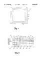
- FIG. 1is a plan view of a semiconductor die according to the present invention.
- FIG. 2is a fragmentary, plan view of an I/O region within the semiconductor die shown in FIG. 1.
- FIG. 3is schematic diagram of a voltage bias generator fabricated within the I/O region shown in FIG. 2.
- FIG. 4is a schematic diagram of an I/O buffer which is biased by the bias voltage generator shown in FIG. 3.
- FIG. 1is a plan view of a semi-conductor die on which the integrated circuit of the present invention is fabricated.
- Die 10is fabricated with a 2.5V fabrication process, for example.
- Die 10includes perimeter 12, scribe region 14, I/O region 16 and core region 18.
- I/O region 16 and core region 18each have a plurality of semiconductor devices or cells.
- I/O region 16extends along scribe region 14 and surrounds core region 18.
- Die 10has a plurality of routing layers for routing interconnections between the devices within I/O region 16 and core region 18.
- Each interconnection or "wire"includes one or more segments of conductive material which is routed in a specified pattern within the various routing layers on die 10.
- Each routing layeris separated from the other routing layers by a dielectric layer.
- FIG. 2is fragmentary plan view of I/O region 16.
- I/O region 16includes I/O slot 20, voltage supply slots 22, 24, 26 and 28 and I/O slot 30.
- Slots 20, 22, 24, 26, 28 and 30include pads 32, 34, 36, 38, 40 and 42, respectively.
- Pads 32, 34, 36, 38, 40 and 42provide an electrical connection to the pins of the integrated circuit package in which die 10 is housed.
- a plurality of global busesextend along I/O region 16, generally parallel to perimeter 102. These buses include I/O voltage supply buses VDDIO and VSSIO, core voltage supply buses VDD2 and VSS2, bias voltage bus BIAS and DC current test buses IDDTN and IDDTNHO. Voltage supply buses VDDIO and VSSIO are coupled to an external power supply through pads 34 and 36, respectively, for supplying and I/O supply voltage to selected devices within I/O region 16. In one embodiment, the external power supply coupled to buses VDDIO and VSSIO supply a 3.3V I/O supply voltage. Voltage supply buses VDD2 and VSS2 are coupled to an external power supply through pads 38 and 40, respectively, for supplying a core supply voltage to selected devices within I/O region 16 and the devices within core region 18. In one embodiment, the external power supply coupled to buses VDD2 and VSS2 supplies a 2.5V core supply voltage.
- Output buffer 50(shown in phantom) is fabricated within I/O slot 20 for interfacing between pad 32 and core region 18 (shown in FIG. 1). As shown in more detail in FIG. 4, output buffer 50 is coupled to each of the supply buses VDDIO, VSSIO, VDD2 and VSS2 and has a bias input coupled to bias voltage bus BIAS.
- Bias voltage generator 52is fabricated within a dedicated area of the voltage supply slots, such as voltage supply slot 22. Bias voltage generator 52 is electrically coupled between I/O supply buses VDDIO and VSSIO and generates a bias voltage on bias voltage bus BIAS, which is used for biasing the various I/O buffers in I/O region 16, such as I/O buffer 50. Since bias voltage generator 52 consumes semiconductor die area, the bias voltage generator is preferably fabricated within one of the voltage supply slots and the bias voltage is routed as a global bus, rather than repeating the bias voltage generator in each of the I/O slots.
- I/O buffer 54is fabricated within I/O slot 30.
- I/O buffer 54is configured as an input-only buffer for receiving a DC current test signal IDDT on pad 42 and generating an inverted test signal on DC current test bus IDDTN.
- the test signal IDDT supplied to pad 42is set to an active state, such as a logic high level.
- the inverted test signal on bus IDDTNis used to shut off all sources of DC current in semiconductor die 10.
- the DC current drawn through voltage supply pads 34, 36, 38 and 40is then measured. If the measured current exceeds a specified tolerance, there may be a short or some other fault condition in semiconductor die 10.
- Voltage level shifting circuit 56is fabricated in voltage supply slot 22 and is coupled between buses IDDTN and IDDTNHO. Voltage level shifting circuit 56 inverts the DC current test signals received on bus IDDTN and shifts the voltage swing of the signals from 0V-2.5V to about 0.8V-3.0V on bus IDDTNHO. Voltage level shifting circuit 56 is described in more detail in U.S. application Ser. No. 08/906,343, filed Aug. 5, 1997 and is entitled "Integrated Circuit I/O Buffer Having Pull-up To Voltages Greater Than Transistor Tolerance," which is assigned to the same assignee and is hereby incorporated by reference.
- FIG. 3is a schematic diagram of bias voltage generator 52, which is electrically coupled to input buffer 54.
- Bias voltage generator 52includes voltage divider 60, feedback circuit 62, pull-up device 64 and power supply decoupled capacitors CUP and CDN.
- Voltage divider 60includes pull-up resistor RUP, pull down resistor RDN and decoupling transistors MPIDDTN1 and MNIDDTN1.
- Pull-up resistor RUPis coupled between voltage supply bus VDDIO, which is at 3.3V, and decoupling transistor MPIDDTN1.
- Decoupling transistor MPIDDTN1has a gate coupled to DC current test bus IDDTNHO, a source coupled to bias voltage output 66 and a drain coupled to pull-up resistor RUP.
- Pull down resistor RDNis coupled between voltage supply bus VSSIO and decoupling transistor MNIDDTN1.
- Decoupling transistor MNIDDTN1has a gate coupled to DC current test bus IDDTN, a source coupled to pull down resistor RDN and a drain coupled to bias voltage output 66.
- Bias voltage output 66is coupled to bias voltage bus BIAS.
- Voltage divider 60generates a selected voltage level on bias voltage output 66, such as 0.8V-1.0V.
- pull-up resistor RUPincludes a 40 K ⁇ resistor and pull down resistor RDN and includes a 16.5 K ⁇ resistor.
- DC current test bus IDDTNis high and DC current test bus IDDTNHO is low, which turns on transistors MPIDDTN1 and MNIDDTN1 and couples pull-up resistor RUP and pull down resistor RDN to bias voltage output 66.
- DC current test bus IDDTNis low and DC current test bus IDDTNHO is high, which turns off transistors MPIDDTN1 and MNIDDTN1 and decouples pull-up resistor RUP and pull down resistor RDN from bias voltage output 66. This shuts off any DC current flowing through voltage divider 60.
- Pull-up device 64includes P-channel transistor MPIDDTN2, which has a gate coupled to DC current test bus IDDTN, a source coupled to voltage supply bus VDD2 and a drain coupled to bias voltage output 66. In test mode, the low level on IDDTN turns on transistor MPIDDTN2 which pulls bias voltage output 66 to a defined voltage such as 2.5V.
- Feedback circuit 62includes inverters 70 and 72, pull-down transistor MN1 and decoupling transistor MNIDDTN2.
- Inverter 70includes N-channel transistor MN2 and P-channel transistor MP1.
- Transistor MN2has a gate coupled to bias voltage output 66, a source coupled to voltage supply terminal VSS2 and a drain coupled to inverter output 74.
- Transistor MP1has a gate coupled to bias voltage output 66, a source coupled to voltage supply terminal VDD2 and a drain coupled to inverter output 74.
- Inverter 72includes N-channel transistor MN3 and P-channel transistor MP2.
- Transistor MN3has a gate coupled to inverter output 74, a source coupled to voltage supply terminal VSS2 and a drain coupled to inverter output 76.
- Transistor MP2has a gate coupled to inverter output 74, a source coupled to voltage supply terminal VDD2 and a drain coupled to inverter output 76.
- Pull-down transistor MN1has a gate coupled to inverter output 76, a source coupled to the drain of decoupling transistor MNIDDTN2 and a drain coupled to bias voltage output 66.
- Decoupling transistor MNIDDTN2has a gate coupled to DC current test bus IDDTN and a source coupled to voltage supply terminal VSS2.
- feedback circuit 62is on only when the voltage level on bias voltage bus BIAS is above a certain threshold level. Above the threshold level, transistor MN2 turns on, pulling inverter output 74 low which turns on transistor MP2. Transistor MP2 pulls inverter output 76 high which turns on transistor MN1, thereby pulling bias voltage bus BIAS back low toward the threshold.
- Bias voltage bus BIASis essentially used as an elevated ground for the I/O buffers in I/O region 16 (shown in FIG. 2). Bias voltage bus BIAS therefore conducts a fair amount of current and should have a fairly low resistance path to ground to prevent the voltage level on the bus from building up.
- Feedback circuit 62provides a low resistance path to ground without significantly increasing current through the resistance path since the feedback circuit is on only when the voltage level on bias voltage bus BIAS exceeds the threshold level.
- Power supply decoupling capacitors CUP and CDNare coupled between bias voltage bus BIAS and voltage supply terminals VDD2 and VSS2, respectively, for suppressing noise in the voltage level on bias voltage bus BIAS. Noise is created when a transistor in I/O region 16 that is coupled to bias voltage bus BIAS changes its output state. The transistor either sinks current from the bus to supply charge to the interconnect capacitance at the transistor output or sources current to the bus to discharge the interconnect capacitance. Power supply decoupling capacitors CUP and CDN have relatively large capacitances, such as 12 pF and 9 pF, respectively, for holding charge that can be used as needed by the I/O transistors.
- Power supply decoupling capacitors CUP and CDNare preferably fabricated within the voltage supply slot in which voltage bias generator 52 is fabricated.
- Power supply decoupling capacitors CUP and CDNcan be formed by applying overlapping conductive segments in two parallel routing layers which are separated by a dielectric layer on the die. The opposing conductive segments are then electrically coupled to bias voltage bus BIAS and the respective voltage supply terminal VDD2 or VSS2 to form the capacitor.
- the conductive segments that form decoupling capacitors CUP and CDNsubstantially fill the available routing area that is dedicated for voltage bias generator 52. This maximizes the decoupling capacitance and thus the charge sharing capacity of the capacitors.
- Capacitors CUP and CDNcan also be formed by PMOS and NMOS transistors having their gates coupled to bias voltage bus BIAS and their sources and drains coupled to VSS2 for PMOS transistors and VDD2 for NMOS transistors.
- FIG. 4is a schematic diagram of I/O buffer 50 which is fabricated within I/O slot 20 (shown in FIG. 2).
- I/O buffer 50is configured as an output-only buffer which receives 0V-2.5V data signals from core region 18 on core terminal A and supplies 0V-3.3V output signals on pad 32.
- I/O buffer 50includes predriver stage 80 and output driver stage 82.
- Predriver stage 80includes pull-up control circuit 84 and pull-down control circuit 86 for controlling the pull-up and pull-down of pad 32 in response to the data signals applied to core terminal A.
- Each transistor in predriver stage 80 and output driver stage 82is biased such that the gate-to-source, gate-to-bulk and gate-to-drain voltages are all less than a 3.0V tolerance to prevent damage to the transistors while driving or receiving 0V-3.3V data signals on pad 32. Also, each transistor is biased such that all drain-to-source voltage are less than a 2.75V tolerance for minimum sized transistors.
- Pull-up control circuit 84includes a voltage level shifting differential amplifier formed by inverter 88, N-differential transistor pair MN4 and MN5, N-channel voltage protection transistors MN6 and MN7, P-channel cross-coupled transistor pair MP3 and MP4 and charge boosting transistors MP5 and MP6.
- Inverter 88is coupled between core terminal A and inverted data terminal AN.
- Transistor MN4has a gate coupled to core terminal A, a source coupled to bias voltage bus BIAS and a drain coupled to node N1.
- Transistor MN5has a gate coupled to inverted data terminal AN, a source coupled to bias voltage bus BIAS and a drain coupled to node N2.
- the drains of transistors MN4 and MN5define first and second current paths I1 and I2 within the differential amplifier.
- the gates of voltage protection transistors MN6 and MN7are coupled to voltage supply terminal VDD2, which is at 2.5V.
- the sources of transistors MN6 and MN7are coupled to nodes N1 and N2, respectively.
- the drains of transistors MN6 and MN7are coupled to nodes ZPBAR and ZP, respectively.
- Transistors MP3 and MP4are cross-coupled to one another, with the gate of transistor MP3 coupled to the drain of transistor MP4 at node ZP and the gate of transistor MP4 coupled to the drain of transistor MP3 at node ZPBAR.
- the sources of transistors MP3 and MP4are coupled to voltage supply terminal VDDIO, which is at 3.3V.
- Node ZPBARis coupled to pull-up control terminal AP.
- Charge boosting transistor MP5has a gate coupled to core terminal A, a source coupled to voltage supply terminal VDD2 and a drain coupled to node N1.
- Charge boosting transistor MP6has a gate coupled to inverted data terminal AN, a source coupled to voltage supply terminal VDD2 and a drain coupled to node N2.
- Pull-up control circuit 84receives the 0V-2.5V data signals on core terminal A and generates inverted and level-shifted 0.8V-3.3V pull-up control signals on node ZPBAR.
- core terminal Ais high at 2.5V, transistor MN4 is on and transistor MN5 is off.
- Transistor MN4pulls current through current path I1, which discharges nodes N1 and ZPBAR toward the voltage level on bias voltage bus BIAS, which is at about 0.8V-1.0V.
- a high, 2.5V voltage on core terminal Atherefore results in a low, 0.8V voltage on node ZPBAR.
- the raised voltage level on bias voltage bus BIASprevents an over voltage condition from the drain-to-source of transistor MP3 when node ZPBAR is pulled low. Extra protection can be obtained by lengthening the gate of transistor MP3 (and transistor MP4) to handle variations in the voltage on voltage supply bus VDDIO.
- the low voltage on node ZPBARturns on transistor MP4 which charges nodes ZP and N2 toward 3.3V.
- Charge boosting transistor MP6is a pull-up transistor which assists transistor MP4 in charging node N2 when the voltage on core terminal A is high.
- the high voltage on node ZPturn off transistor MP3.
- transistor MN7turns off and thereafter prevents further charging of node N2. This prevents the gate-to-drain voltage of transistor MN5 from exceeding the 3.0V tolerance.
- transistor MN4When the voltage on core terminal A is low, transistor MN4 is off and transistor MN5 is on. Transistor MN5 discharges nodes N2 and ZP toward 0.8V. The low voltage on node ZP turns on transistor MP3 which charges nodes ZPBAR and N1 toward 3.3V. Charge boosting transistor MP5 is pull-up transistor which assists transistor MP3 in charging node N1 when the data on core terminal A is low. As node N1 reaches an NMOS threshold voltage below 2.5V, transistor MN6 turns of since its gate is tied to voltage supply terminal VDD2. This prevents further charging of node N1 and thereby protects transistor MN4 from an over voltage condition. The high voltage on node ZPBAR turns off transistor MP4. The low, 0V voltage on core terminal A therefore results in a high, 3.3V voltage on node ZPBAR.
- Pull-down control circuit 86receives the 0V-2.5V data signals on core terminal A and generates inverted, 0V-2.5V pull-down control signals on pull-down control terminal AN.
- Pull-down control circuit 86includes inverters 88, 90, 92, 94 and 96 which are coupled together in series between core terminal and pull-down control terminal AN.
- Inverters 88, 90, 92 and 94form a delay line to the input of inverter 96.
- Inverter 96includes N-channel transistor MN7 and P-channel transistors MP7 and MP8.
- Transistor MN8has a gate coupled to core terminal A, a source coupled to voltage supply terminal VSS2 and a drain coupled to pull-up control terminal AN.
- Transistor MP7has a gate coupled to the output of inverter 94, a source coupled to the drain of transistor MP8 and drain coupled to pull-down control terminal AN.
- Transistor MP8has a gate coupled to core terminal A and a source coupled to voltage supply terminal VDD2.
- a low-to-high transition on core terminal Abypasses the delay line formed by inverters 88, 92 and 94 and quickly pulls terminal AN low through transistor MN8.
- a high-to-low transition on core terminal Amust pass through the delay line before pulling terminal AN high through transistors MP7 and MP8.
- Output driver stage 82includes P-channel pull-up transistor MP9, P-channel voltage protection transistor MP10, N-channel pull-down transistor MN9 and N-channel voltage protection transistor MN10 which are coupled together in series between voltage supply terminal VDDIO and voltage supply terminal VSSIO.
- Pull-up transistor MP9has a gate coupled to pull-up control terminal AP, a source coupled to voltage supply terminal VDDIO and a drain coupled to node ZP1.
- Voltage protection transistor MP10has a gate coupled to bias voltage bus BIAS, a source coupled to node ZP1 and a drain coupled to output node Z.
- Pull-down transistor MN9has a gate coupled to pull-down control terminal AN, a source coupled to voltage supply terminal VSSIO and drain coupled to node ZN1.
- Voltage protection transistor MN10has a gate coupled to voltage supply terminal VDD2, a source coupled to node ZN1 and a drain coupled to output node Z.
- Electrostatic discharge (ESD) protection resistor R1is coupled
- pull-up control terminal APWhen the data on core terminal A is at 2.5V, pull-up control terminal AP is at 0.8V and pull-down control terminal AN is at 0V.
- Pull-up transistor MP9is on and pull-down transistor MN9 is off.
- Pull-up transistor MP9charges nodes ZP1, Z and ZN1 toward 3.3V.
- node ZN1reaches an NMOS threshold voltage below the gate of voltage protection transistor MN10, which is at 2.5V
- transistor MN10turns off. This prevents further charging of node ZN1 and an over voltage condition with respect to the gate of pull-down transistor MN9 which is at 0V.
- pull-up control terminal APWhen the data on core terminal A is at 0V, pull-up control terminal AP is at 3.3V and pull-down control AN is at 2.5V.
- Pull-up transistor MP9is off and pull-down transistor MN9 is on.
- Pull-down transistor MN9discharges nodes ZN1, Z and ZP toward 0V.
- transistor MP10turns off preventing further discharge of node ZP1 and an over voltage condition with respect to the gate of pull-up transistor MP9 which is at 3.3V.
- I/O buffer 50therefore drives 0V-3.3V data signals on I/O pad 32 without exceeding the transistor tolerances of any of the transistors in the circuit.
- the bias voltage generatorin one of the voltage supply slots in the I/O region and routing the bias voltage output as a global bus, as opposed to fabricating the bias voltage generator in each I/O slot, conserves semiconductor real estate and reduces power consumption.
- the bias voltage generatorgenerates a bias voltage level with two ratioed N-well resistors rather than transistor biasing. The bias voltage level is therefore substantially independent of transistor characteristic variations.
- the bias voltage generatorhas a very low DC current since the feedback circuit is on only when the voltage level on the bias voltage bus exceeds a predetermined threshold level. In one embodiment, the bias voltage generator has a worst case DC current of about 50 microamperes.
- bias voltage generatorin the voltage supply slots.
- the current drawn the by the bias voltage generatoris dependent on the number of voltage supply slots rather than the number of I/O slots.
- bias voltage levelis dependent on the level of the I/O supply voltage. When the I/O supply voltage level increases, the bias voltage level increases and thus the voltage protection provided by the raised bias voltage level also increases.
- the present inventioncan be implemented with various technologies, including CMOS, and can have a variety of circuit configurations.
- the transistors shown in the figurescan include individual transistors or an array of transistors coupled together in parallel with one another.
- the voltage supply terminalscan be relatively positive or relatively negative, depending upon the particular convention adopted and the technology used.
- the terms "pull-up” and “pull-down” used in the specification and the claimsare arbitrary terms and can refer either to a logic high level or a logic low level depending upon the relative levels of the voltage supply terminals.
- the term “coupled”can include various types of connections or couplings and can include a direct connection or a connection through one or more intermediate components.
Landscapes
- Engineering & Computer Science (AREA)
- Physics & Mathematics (AREA)
- Radar, Positioning & Navigation (AREA)
- Nonlinear Science (AREA)
- Electromagnetism (AREA)
- General Physics & Mathematics (AREA)
- Microelectronics & Electronic Packaging (AREA)
- Automation & Control Theory (AREA)
- Computer Hardware Design (AREA)
- Computing Systems (AREA)
- General Engineering & Computer Science (AREA)
- Mathematical Physics (AREA)
- Semiconductor Integrated Circuits (AREA)
Abstract
Description
Claims (19)
Priority Applications (1)
| Application Number | Priority Date | Filing Date | Title |
|---|---|---|---|
| US08/910,730US5963057A (en) | 1997-08-05 | 1997-08-13 | Chip level bias for buffers driving voltages greater than transistor tolerance |
Applications Claiming Priority (2)
| Application Number | Priority Date | Filing Date | Title |
|---|---|---|---|
| US08/906,343US6028449A (en) | 1997-08-05 | 1997-08-05 | Integrated circuit I/O buffer having pull-up to voltages greater than transistor tolerance |
| US08/910,730US5963057A (en) | 1997-08-05 | 1997-08-13 | Chip level bias for buffers driving voltages greater than transistor tolerance |
Related Parent Applications (1)
| Application Number | Title | Priority Date | Filing Date |
|---|---|---|---|
| US08/906,343Continuation-In-PartUS6028449A (en) | 1997-08-05 | 1997-08-05 | Integrated circuit I/O buffer having pull-up to voltages greater than transistor tolerance |
Publications (1)
| Publication Number | Publication Date |
|---|---|
| US5963057Atrue US5963057A (en) | 1999-10-05 |
Family
ID=46253597
Family Applications (1)
| Application Number | Title | Priority Date | Filing Date |
|---|---|---|---|
| US08/910,730Expired - LifetimeUS5963057A (en) | 1997-08-05 | 1997-08-13 | Chip level bias for buffers driving voltages greater than transistor tolerance |
Country Status (1)
| Country | Link |
|---|---|
| US (1) | US5963057A (en) |
Cited By (14)
| Publication number | Priority date | Publication date | Assignee | Title |
|---|---|---|---|---|
| US6300800B1 (en) | 1999-11-24 | 2001-10-09 | Lsi Logic Corporation | Integrated circuit I/O buffer with series P-channel and floating well |
| US6300752B1 (en)* | 1999-05-24 | 2001-10-09 | Level One Communications, Inc. | Common mode bias voltage generator |
| US6330679B1 (en)* | 1997-12-31 | 2001-12-11 | Intel Corporation | Input buffer circuit with dual power down functions |
| US6342802B1 (en) | 1999-10-28 | 2002-01-29 | Seagate Technology Llc | Multi-voltage power-up stable input/output buffer circuit in a disc drive |
| US6462989B1 (en)* | 2001-05-30 | 2002-10-08 | Micron Technology, Inc. | Technique for locally reducing effects on an analog signal due to changes on a reference bus in an integrated circuit |
| US6509725B1 (en) | 2001-11-09 | 2003-01-21 | International Business Machines Corporation | Self-regulating voltage divider for series-stacked voltage rails |
| US6617891B2 (en)* | 2001-09-26 | 2003-09-09 | Intel Corporation | Slew rate at buffers by isolating predriver from driver |
| US20030210087A1 (en)* | 2001-10-05 | 2003-11-13 | Mitsubishi Denki Kabushiki Kaisha | Integrated circuit |
| US6813672B1 (en)* | 2001-02-23 | 2004-11-02 | Cypress Semiconductor Corp. | EMC enhancement for differential devices |
| US7551909B1 (en)* | 2002-08-29 | 2009-06-23 | Silicon Image, Inc. | CMOS transceiver with dual current path VCO |
| US7689724B1 (en) | 2002-08-16 | 2010-03-30 | Cypress Semiconductor Corporation | Apparatus, system and method for sharing data from a device between multiple computers |
| US7765344B2 (en) | 2002-09-27 | 2010-07-27 | Cypress Semiconductor Corporation | Apparatus and method for dynamically providing hub or host operations |
| US20100321083A1 (en)* | 2009-06-22 | 2010-12-23 | International Business Machines Corporation | Voltage Level Translating Circuit |
| US20210242871A1 (en)* | 2020-01-31 | 2021-08-05 | Nxp Usa, Inc. | Multivoltage high voltage io in low voltage technology |
Citations (15)
| Publication number | Priority date | Publication date | Assignee | Title |
|---|---|---|---|---|
| US4978633A (en)* | 1989-08-22 | 1990-12-18 | Harris Corporation | Hierarchical variable die size gate array architecture |
| US5001487A (en)* | 1985-01-25 | 1991-03-19 | Hitachi, Ltd. | Semiconductor integrated circuit device |
| US5003204A (en)* | 1989-12-19 | 1991-03-26 | Bull Hn Information Systems Inc. | Edge triggered D-type flip-flop scan latch cell with recirculation capability |
| US5266849A (en)* | 1992-02-19 | 1993-11-30 | Hal Computer Systems, Inc. | Tri state buffer circuit for dual power system |
| US5300832A (en)* | 1992-11-10 | 1994-04-05 | Sun Microsystems, Inc. | Voltage interfacing buffer with isolation transistors used for overvoltage protection |
| US5321324A (en)* | 1993-01-28 | 1994-06-14 | United Memories, Inc. | Low-to-high voltage translator with latch-up immunity |
| US5338978A (en)* | 1993-02-10 | 1994-08-16 | National Semiconductor Corporation | Full swing power down buffer circuit with multiple power supply isolation |
| US5406141A (en)* | 1992-07-06 | 1995-04-11 | Sgs-Thomson Microelectronics, S.A. | High voltage CMOS switching circuit |
| US5410267A (en)* | 1993-09-24 | 1995-04-25 | Intel Corporation | 3.3 V to 5 V supply interface buffer |
| US5418476A (en)* | 1994-07-28 | 1995-05-23 | At&T Corp. | Low voltage output buffer with improved speed |
| US5450025A (en)* | 1993-02-10 | 1995-09-12 | National Semiconductor Corporation | Tristate driver for interfacing to a bus subject to overvoltage conditions |
| US5467031A (en)* | 1994-09-22 | 1995-11-14 | Lsi Logic Corporation | 3.3 volt CMOS tri-state driver circuit capable of driving common 5 volt line |
| US5537059A (en)* | 1992-12-24 | 1996-07-16 | Mitsubishi Denki Kabushiki Kaisha | Output circuit of semiconductor integrated circuit device |
| US5559464A (en)* | 1993-07-06 | 1996-09-24 | Seiko Epson Corporation | Signal voltage level conversion circuit and output buffer circuit |
| US5736869A (en)* | 1996-05-16 | 1998-04-07 | Lsi Logic Corporation | Output driver with level shifting and voltage protection |
- 1997
- 1997-08-13USUS08/910,730patent/US5963057A/ennot_activeExpired - Lifetime
Patent Citations (15)
| Publication number | Priority date | Publication date | Assignee | Title |
|---|---|---|---|---|
| US5001487A (en)* | 1985-01-25 | 1991-03-19 | Hitachi, Ltd. | Semiconductor integrated circuit device |
| US4978633A (en)* | 1989-08-22 | 1990-12-18 | Harris Corporation | Hierarchical variable die size gate array architecture |
| US5003204A (en)* | 1989-12-19 | 1991-03-26 | Bull Hn Information Systems Inc. | Edge triggered D-type flip-flop scan latch cell with recirculation capability |
| US5266849A (en)* | 1992-02-19 | 1993-11-30 | Hal Computer Systems, Inc. | Tri state buffer circuit for dual power system |
| US5406141A (en)* | 1992-07-06 | 1995-04-11 | Sgs-Thomson Microelectronics, S.A. | High voltage CMOS switching circuit |
| US5300832A (en)* | 1992-11-10 | 1994-04-05 | Sun Microsystems, Inc. | Voltage interfacing buffer with isolation transistors used for overvoltage protection |
| US5537059A (en)* | 1992-12-24 | 1996-07-16 | Mitsubishi Denki Kabushiki Kaisha | Output circuit of semiconductor integrated circuit device |
| US5321324A (en)* | 1993-01-28 | 1994-06-14 | United Memories, Inc. | Low-to-high voltage translator with latch-up immunity |
| US5338978A (en)* | 1993-02-10 | 1994-08-16 | National Semiconductor Corporation | Full swing power down buffer circuit with multiple power supply isolation |
| US5450025A (en)* | 1993-02-10 | 1995-09-12 | National Semiconductor Corporation | Tristate driver for interfacing to a bus subject to overvoltage conditions |
| US5559464A (en)* | 1993-07-06 | 1996-09-24 | Seiko Epson Corporation | Signal voltage level conversion circuit and output buffer circuit |
| US5410267A (en)* | 1993-09-24 | 1995-04-25 | Intel Corporation | 3.3 V to 5 V supply interface buffer |
| US5418476A (en)* | 1994-07-28 | 1995-05-23 | At&T Corp. | Low voltage output buffer with improved speed |
| US5467031A (en)* | 1994-09-22 | 1995-11-14 | Lsi Logic Corporation | 3.3 volt CMOS tri-state driver circuit capable of driving common 5 volt line |
| US5736869A (en)* | 1996-05-16 | 1998-04-07 | Lsi Logic Corporation | Output driver with level shifting and voltage protection |
Cited By (20)
| Publication number | Priority date | Publication date | Assignee | Title |
|---|---|---|---|---|
| US6330679B1 (en)* | 1997-12-31 | 2001-12-11 | Intel Corporation | Input buffer circuit with dual power down functions |
| US6300752B1 (en)* | 1999-05-24 | 2001-10-09 | Level One Communications, Inc. | Common mode bias voltage generator |
| US6417655B2 (en)* | 1999-05-24 | 2002-07-09 | Level One Communications, Inc. | Common mode bias voltage generator |
| US6342802B1 (en) | 1999-10-28 | 2002-01-29 | Seagate Technology Llc | Multi-voltage power-up stable input/output buffer circuit in a disc drive |
| US6300800B1 (en) | 1999-11-24 | 2001-10-09 | Lsi Logic Corporation | Integrated circuit I/O buffer with series P-channel and floating well |
| US6813672B1 (en)* | 2001-02-23 | 2004-11-02 | Cypress Semiconductor Corp. | EMC enhancement for differential devices |
| US6462989B1 (en)* | 2001-05-30 | 2002-10-08 | Micron Technology, Inc. | Technique for locally reducing effects on an analog signal due to changes on a reference bus in an integrated circuit |
| US6587379B2 (en) | 2001-05-30 | 2003-07-01 | Micron Technology, Inc. | Electronic device with locally reduced effects on analog signals |
| US6617891B2 (en)* | 2001-09-26 | 2003-09-09 | Intel Corporation | Slew rate at buffers by isolating predriver from driver |
| US20030210088A1 (en)* | 2001-10-05 | 2003-11-13 | Mitsubishi Denki Kabushiki Kaisha | Integrated circuit |
| US20030210087A1 (en)* | 2001-10-05 | 2003-11-13 | Mitsubishi Denki Kabushiki Kaisha | Integrated circuit |
| US6747502B2 (en) | 2001-10-05 | 2004-06-08 | Mitsubishi Denki Kabushiki Kaisha | Level shift circuit including a resistor configured to drive a high-withstand-voltage element |
| US6927617B2 (en)* | 2001-10-05 | 2005-08-09 | Mitsubishi Denki Kabushiki Kaisha | Integrated circuit |
| US6509725B1 (en) | 2001-11-09 | 2003-01-21 | International Business Machines Corporation | Self-regulating voltage divider for series-stacked voltage rails |
| US7689724B1 (en) | 2002-08-16 | 2010-03-30 | Cypress Semiconductor Corporation | Apparatus, system and method for sharing data from a device between multiple computers |
| US7551909B1 (en)* | 2002-08-29 | 2009-06-23 | Silicon Image, Inc. | CMOS transceiver with dual current path VCO |
| US7765344B2 (en) | 2002-09-27 | 2010-07-27 | Cypress Semiconductor Corporation | Apparatus and method for dynamically providing hub or host operations |
| US20100321083A1 (en)* | 2009-06-22 | 2010-12-23 | International Business Machines Corporation | Voltage Level Translating Circuit |
| US20210242871A1 (en)* | 2020-01-31 | 2021-08-05 | Nxp Usa, Inc. | Multivoltage high voltage io in low voltage technology |
| US11108396B2 (en)* | 2020-01-31 | 2021-08-31 | Nxp Usa, Inc. | Multivoltage high voltage IO in low voltage technology |
Similar Documents
| Publication | Publication Date | Title |
|---|---|---|
| US6130556A (en) | Integrated circuit I/O buffer with 5V well and passive gate voltage | |
| US5736869A (en) | Output driver with level shifting and voltage protection | |
| US6005413A (en) | 5V tolerant PCI I/O buffer on 2.5V technology | |
| US5956219A (en) | High voltage power supply clamp circuitry for electrostatic discharge (ESD) protection | |
| US6028449A (en) | Integrated circuit I/O buffer having pull-up to voltages greater than transistor tolerance | |
| US5963057A (en) | Chip level bias for buffers driving voltages greater than transistor tolerance | |
| US6300800B1 (en) | Integrated circuit I/O buffer with series P-channel and floating well | |
| US5966030A (en) | Output buffer with regulated voltage biasing for driving voltages greater than transistor tolerance | |
| US6118303A (en) | Integrated circuit I/O buffer having pass gate protection with RC delay | |
| US8310275B2 (en) | High voltage tolerant input/output interface circuit | |
| US5329174A (en) | Circuit for forcing known voltage on unconnected pads of an integrated circuit | |
| JP2000077996A (en) | Interface circuit | |
| JP3478992B2 (en) | High voltage and extensible driver circuit | |
| US6249146B1 (en) | MOS output buffer with overvoltage protection circuitry | |
| JP3266527B2 (en) | Output driver circuit and semiconductor device | |
| US7430100B2 (en) | Buffer circuit with enhanced overvoltage protection | |
| JP3258229B2 (en) | Level conversion circuit and semiconductor integrated circuit | |
| US5900750A (en) | 5V output driver on 2.5V technology | |
| US4845388A (en) | TTL-CMOS input buffer | |
| US4503341A (en) | Power-down inverter circuit | |
| US6384632B2 (en) | Buffer circuit | |
| US7394291B2 (en) | High voltage tolerant output buffer | |
| US20250096559A1 (en) | Power clamp circuit and electronic device including power clamp circuit | |
| JPH03116864A (en) | Cmos semiconductor integrated circuit device | |
| JP3883114B2 (en) | Semiconductor device |
Legal Events
| Date | Code | Title | Description |
|---|---|---|---|
| AS | Assignment | Owner name:LSI LOGIC CORPORATION, CALIFORNIA Free format text:ASSIGNMENT OF ASSIGNORS INTEREST;ASSIGNORS:SCHMITT, JONATHAN;TORGERSON, PAUL;REEL/FRAME:008681/0345 Effective date:19970812 | |
| STCF | Information on status: patent grant | Free format text:PATENTED CASE | |
| FPAY | Fee payment | Year of fee payment:4 | |
| FPAY | Fee payment | Year of fee payment:8 | |
| FEPP | Fee payment procedure | Free format text:PAYER NUMBER DE-ASSIGNED (ORIGINAL EVENT CODE: RMPN); ENTITY STATUS OF PATENT OWNER: LARGE ENTITY Free format text:PAYOR NUMBER ASSIGNED (ORIGINAL EVENT CODE: ASPN); ENTITY STATUS OF PATENT OWNER: LARGE ENTITY | |
| FPAY | Fee payment | Year of fee payment:12 | |
| AS | Assignment | Owner name:DEUTSCHE BANK AG NEW YORK BRANCH, AS COLLATERAL AG Free format text:PATENT SECURITY AGREEMENT;ASSIGNORS:LSI CORPORATION;AGERE SYSTEMS LLC;REEL/FRAME:032856/0031 Effective date:20140506 | |
| AS | Assignment | Owner name:LSI CORPORATION, CALIFORNIA Free format text:CHANGE OF NAME;ASSIGNOR:LSI LOGIC CORPORATION;REEL/FRAME:033102/0270 Effective date:20070406 | |
| AS | Assignment | Owner name:AVAGO TECHNOLOGIES GENERAL IP (SINGAPORE) PTE. LTD Free format text:ASSIGNMENT OF ASSIGNORS INTEREST;ASSIGNOR:LSI CORPORATION;REEL/FRAME:035390/0388 Effective date:20140814 | |
| AS | Assignment | Owner name:AGERE SYSTEMS LLC, PENNSYLVANIA Free format text:TERMINATION AND RELEASE OF SECURITY INTEREST IN PATENT RIGHTS (RELEASES RF 032856-0031);ASSIGNOR:DEUTSCHE BANK AG NEW YORK BRANCH, AS COLLATERAL AGENT;REEL/FRAME:037684/0039 Effective date:20160201 Owner name:LSI CORPORATION, CALIFORNIA Free format text:TERMINATION AND RELEASE OF SECURITY INTEREST IN PATENT RIGHTS (RELEASES RF 032856-0031);ASSIGNOR:DEUTSCHE BANK AG NEW YORK BRANCH, AS COLLATERAL AGENT;REEL/FRAME:037684/0039 Effective date:20160201 | |
| AS | Assignment | Owner name:BANK OF AMERICA, N.A., AS COLLATERAL AGENT, NORTH CAROLINA Free format text:PATENT SECURITY AGREEMENT;ASSIGNOR:AVAGO TECHNOLOGIES GENERAL IP (SINGAPORE) PTE. LTD.;REEL/FRAME:037808/0001 Effective date:20160201 Owner name:BANK OF AMERICA, N.A., AS COLLATERAL AGENT, NORTH Free format text:PATENT SECURITY AGREEMENT;ASSIGNOR:AVAGO TECHNOLOGIES GENERAL IP (SINGAPORE) PTE. LTD.;REEL/FRAME:037808/0001 Effective date:20160201 | |
| AS | Assignment | Owner name:AVAGO TECHNOLOGIES GENERAL IP (SINGAPORE) PTE. LTD., SINGAPORE Free format text:TERMINATION AND RELEASE OF SECURITY INTEREST IN PATENTS;ASSIGNOR:BANK OF AMERICA, N.A., AS COLLATERAL AGENT;REEL/FRAME:041710/0001 Effective date:20170119 Owner name:AVAGO TECHNOLOGIES GENERAL IP (SINGAPORE) PTE. LTD Free format text:TERMINATION AND RELEASE OF SECURITY INTEREST IN PATENTS;ASSIGNOR:BANK OF AMERICA, N.A., AS COLLATERAL AGENT;REEL/FRAME:041710/0001 Effective date:20170119 |