US5962917A - Semiconductor device package having end-face halved through-holes and inside-area through-holes - Google Patents
Semiconductor device package having end-face halved through-holes and inside-area through-holesDownload PDFInfo
- Publication number
- US5962917A US5962917AUS09/050,940US5094098AUS5962917AUS 5962917 AUS5962917 AUS 5962917AUS 5094098 AUS5094098 AUS 5094098AUS 5962917 AUS5962917 AUS 5962917A
- Authority
- US
- United States
- Prior art keywords
- holes
- face
- halved
- circuit substrate
- semiconductor device
- Prior art date
- Legal status (The legal status is an assumption and is not a legal conclusion. Google has not performed a legal analysis and makes no representation as to the accuracy of the status listed.)
- Expired - Fee Related
Links
Images


Classifications
- H—ELECTRICITY
- H01—ELECTRIC ELEMENTS
- H01L—SEMICONDUCTOR DEVICES NOT COVERED BY CLASS H10
- H01L23/00—Details of semiconductor or other solid state devices
- H01L23/28—Encapsulations, e.g. encapsulating layers, coatings, e.g. for protection
- H01L23/31—Encapsulations, e.g. encapsulating layers, coatings, e.g. for protection characterised by the arrangement or shape
- H01L23/3107—Encapsulations, e.g. encapsulating layers, coatings, e.g. for protection characterised by the arrangement or shape the device being completely enclosed
- H01L23/3121—Encapsulations, e.g. encapsulating layers, coatings, e.g. for protection characterised by the arrangement or shape the device being completely enclosed a substrate forming part of the encapsulation
- H01L23/3128—Encapsulations, e.g. encapsulating layers, coatings, e.g. for protection characterised by the arrangement or shape the device being completely enclosed a substrate forming part of the encapsulation the substrate having spherical bumps for external connection
- H—ELECTRICITY
- H01—ELECTRIC ELEMENTS
- H01L—SEMICONDUCTOR DEVICES NOT COVERED BY CLASS H10
- H01L23/00—Details of semiconductor or other solid state devices
- H01L23/48—Arrangements for conducting electric current to or from the solid state body in operation, e.g. leads, terminal arrangements ; Selection of materials therefor
- H01L23/488—Arrangements for conducting electric current to or from the solid state body in operation, e.g. leads, terminal arrangements ; Selection of materials therefor consisting of soldered or bonded constructions
- H01L23/498—Leads, i.e. metallisations or lead-frames on insulating substrates, e.g. chip carriers
- H01L23/49805—Leads, i.e. metallisations or lead-frames on insulating substrates, e.g. chip carriers the leads being also applied on the sidewalls or the bottom of the substrate, e.g. leadless packages for surface mounting
- H—ELECTRICITY
- H01—ELECTRIC ELEMENTS
- H01L—SEMICONDUCTOR DEVICES NOT COVERED BY CLASS H10
- H01L23/00—Details of semiconductor or other solid state devices
- H01L23/48—Arrangements for conducting electric current to or from the solid state body in operation, e.g. leads, terminal arrangements ; Selection of materials therefor
- H01L23/488—Arrangements for conducting electric current to or from the solid state body in operation, e.g. leads, terminal arrangements ; Selection of materials therefor consisting of soldered or bonded constructions
- H01L23/498—Leads, i.e. metallisations or lead-frames on insulating substrates, e.g. chip carriers
- H01L23/49811—Additional leads joined to the metallisation on the insulating substrate, e.g. pins, bumps, wires, flat leads
- H01L23/49816—Spherical bumps on the substrate for external connection, e.g. ball grid arrays [BGA]
- H—ELECTRICITY
- H01—ELECTRIC ELEMENTS
- H01L—SEMICONDUCTOR DEVICES NOT COVERED BY CLASS H10
- H01L23/00—Details of semiconductor or other solid state devices
- H01L23/48—Arrangements for conducting electric current to or from the solid state body in operation, e.g. leads, terminal arrangements ; Selection of materials therefor
- H01L23/488—Arrangements for conducting electric current to or from the solid state body in operation, e.g. leads, terminal arrangements ; Selection of materials therefor consisting of soldered or bonded constructions
- H01L23/498—Leads, i.e. metallisations or lead-frames on insulating substrates, e.g. chip carriers
- H01L23/49827—Via connections through the substrates, e.g. pins going through the substrate, coaxial cables
- H—ELECTRICITY
- H05—ELECTRIC TECHNIQUES NOT OTHERWISE PROVIDED FOR
- H05K—PRINTED CIRCUITS; CASINGS OR CONSTRUCTIONAL DETAILS OF ELECTRIC APPARATUS; MANUFACTURE OF ASSEMBLAGES OF ELECTRICAL COMPONENTS
- H05K3/00—Apparatus or processes for manufacturing printed circuits
- H05K3/30—Assembling printed circuits with electric components, e.g. with resistor
- H05K3/32—Assembling printed circuits with electric components, e.g. with resistor electrically connecting electric components or wires to printed circuits
- H05K3/34—Assembling printed circuits with electric components, e.g. with resistor electrically connecting electric components or wires to printed circuits by soldering
- H05K3/3452—Solder masks
- H—ELECTRICITY
- H01—ELECTRIC ELEMENTS
- H01L—SEMICONDUCTOR DEVICES NOT COVERED BY CLASS H10
- H01L2224/00—Indexing scheme for arrangements for connecting or disconnecting semiconductor or solid-state bodies and methods related thereto as covered by H01L24/00
- H01L2224/01—Means for bonding being attached to, or being formed on, the surface to be connected, e.g. chip-to-package, die-attach, "first-level" interconnects; Manufacturing methods related thereto
- H01L2224/26—Layer connectors, e.g. plate connectors, solder or adhesive layers; Manufacturing methods related thereto
- H01L2224/31—Structure, shape, material or disposition of the layer connectors after the connecting process
- H01L2224/32—Structure, shape, material or disposition of the layer connectors after the connecting process of an individual layer connector
- H01L2224/321—Disposition
- H01L2224/32151—Disposition the layer connector connecting between a semiconductor or solid-state body and an item not being a semiconductor or solid-state body, e.g. chip-to-substrate, chip-to-passive
- H01L2224/32221—Disposition the layer connector connecting between a semiconductor or solid-state body and an item not being a semiconductor or solid-state body, e.g. chip-to-substrate, chip-to-passive the body and the item being stacked
- H01L2224/32225—Disposition the layer connector connecting between a semiconductor or solid-state body and an item not being a semiconductor or solid-state body, e.g. chip-to-substrate, chip-to-passive the body and the item being stacked the item being non-metallic, e.g. insulating substrate with or without metallisation
- H—ELECTRICITY
- H01—ELECTRIC ELEMENTS
- H01L—SEMICONDUCTOR DEVICES NOT COVERED BY CLASS H10
- H01L2224/00—Indexing scheme for arrangements for connecting or disconnecting semiconductor or solid-state bodies and methods related thereto as covered by H01L24/00
- H01L2224/01—Means for bonding being attached to, or being formed on, the surface to be connected, e.g. chip-to-package, die-attach, "first-level" interconnects; Manufacturing methods related thereto
- H01L2224/42—Wire connectors; Manufacturing methods related thereto
- H01L2224/47—Structure, shape, material or disposition of the wire connectors after the connecting process
- H01L2224/48—Structure, shape, material or disposition of the wire connectors after the connecting process of an individual wire connector
- H01L2224/481—Disposition
- H01L2224/48151—Connecting between a semiconductor or solid-state body and an item not being a semiconductor or solid-state body, e.g. chip-to-substrate, chip-to-passive
- H01L2224/48221—Connecting between a semiconductor or solid-state body and an item not being a semiconductor or solid-state body, e.g. chip-to-substrate, chip-to-passive the body and the item being stacked
- H01L2224/48225—Connecting between a semiconductor or solid-state body and an item not being a semiconductor or solid-state body, e.g. chip-to-substrate, chip-to-passive the body and the item being stacked the item being non-metallic, e.g. insulating substrate with or without metallisation
- H01L2224/48227—Connecting between a semiconductor or solid-state body and an item not being a semiconductor or solid-state body, e.g. chip-to-substrate, chip-to-passive the body and the item being stacked the item being non-metallic, e.g. insulating substrate with or without metallisation connecting the wire to a bond pad of the item
- H—ELECTRICITY
- H01—ELECTRIC ELEMENTS
- H01L—SEMICONDUCTOR DEVICES NOT COVERED BY CLASS H10
- H01L2224/00—Indexing scheme for arrangements for connecting or disconnecting semiconductor or solid-state bodies and methods related thereto as covered by H01L24/00
- H01L2224/01—Means for bonding being attached to, or being formed on, the surface to be connected, e.g. chip-to-package, die-attach, "first-level" interconnects; Manufacturing methods related thereto
- H01L2224/42—Wire connectors; Manufacturing methods related thereto
- H01L2224/47—Structure, shape, material or disposition of the wire connectors after the connecting process
- H01L2224/48—Structure, shape, material or disposition of the wire connectors after the connecting process of an individual wire connector
- H01L2224/484—Connecting portions
- H01L2224/48463—Connecting portions the connecting portion on the bonding area of the semiconductor or solid-state body being a ball bond
- H01L2224/48465—Connecting portions the connecting portion on the bonding area of the semiconductor or solid-state body being a ball bond the other connecting portion not on the bonding area being a wedge bond, i.e. ball-to-wedge, regular stitch
- H—ELECTRICITY
- H01—ELECTRIC ELEMENTS
- H01L—SEMICONDUCTOR DEVICES NOT COVERED BY CLASS H10
- H01L2224/00—Indexing scheme for arrangements for connecting or disconnecting semiconductor or solid-state bodies and methods related thereto as covered by H01L24/00
- H01L2224/73—Means for bonding being of different types provided for in two or more of groups H01L2224/10, H01L2224/18, H01L2224/26, H01L2224/34, H01L2224/42, H01L2224/50, H01L2224/63, H01L2224/71
- H01L2224/732—Location after the connecting process
- H01L2224/73251—Location after the connecting process on different surfaces
- H01L2224/73265—Layer and wire connectors
- H—ELECTRICITY
- H01—ELECTRIC ELEMENTS
- H01L—SEMICONDUCTOR DEVICES NOT COVERED BY CLASS H10
- H01L24/00—Arrangements for connecting or disconnecting semiconductor or solid-state bodies; Methods or apparatus related thereto
- H01L24/01—Means for bonding being attached to, or being formed on, the surface to be connected, e.g. chip-to-package, die-attach, "first-level" interconnects; Manufacturing methods related thereto
- H01L24/42—Wire connectors; Manufacturing methods related thereto
- H01L24/47—Structure, shape, material or disposition of the wire connectors after the connecting process
- H01L24/48—Structure, shape, material or disposition of the wire connectors after the connecting process of an individual wire connector
- H—ELECTRICITY
- H01—ELECTRIC ELEMENTS
- H01L—SEMICONDUCTOR DEVICES NOT COVERED BY CLASS H10
- H01L24/00—Arrangements for connecting or disconnecting semiconductor or solid-state bodies; Methods or apparatus related thereto
- H01L24/73—Means for bonding being of different types provided for in two or more of groups H01L24/10, H01L24/18, H01L24/26, H01L24/34, H01L24/42, H01L24/50, H01L24/63, H01L24/71
- H—ELECTRICITY
- H01—ELECTRIC ELEMENTS
- H01L—SEMICONDUCTOR DEVICES NOT COVERED BY CLASS H10
- H01L2924/00—Indexing scheme for arrangements or methods for connecting or disconnecting semiconductor or solid-state bodies as covered by H01L24/00
- H01L2924/0001—Technical content checked by a classifier
- H01L2924/00014—Technical content checked by a classifier the subject-matter covered by the group, the symbol of which is combined with the symbol of this group, being disclosed without further technical details
- H—ELECTRICITY
- H01—ELECTRIC ELEMENTS
- H01L—SEMICONDUCTOR DEVICES NOT COVERED BY CLASS H10
- H01L2924/00—Indexing scheme for arrangements or methods for connecting or disconnecting semiconductor or solid-state bodies as covered by H01L24/00
- H01L2924/095—Indexing scheme for arrangements or methods for connecting or disconnecting semiconductor or solid-state bodies as covered by H01L24/00 with a principal constituent of the material being a combination of two or more materials provided in the groups H01L2924/013 - H01L2924/0715
- H01L2924/097—Glass-ceramics, e.g. devitrified glass
- H01L2924/09701—Low temperature co-fired ceramic [LTCC]
- H—ELECTRICITY
- H01—ELECTRIC ELEMENTS
- H01L—SEMICONDUCTOR DEVICES NOT COVERED BY CLASS H10
- H01L2924/00—Indexing scheme for arrangements or methods for connecting or disconnecting semiconductor or solid-state bodies as covered by H01L24/00
- H01L2924/15—Details of package parts other than the semiconductor or other solid state devices to be connected
- H01L2924/151—Die mounting substrate
- H01L2924/1515—Shape
- H01L2924/15153—Shape the die mounting substrate comprising a recess for hosting the device
- H—ELECTRICITY
- H01—ELECTRIC ELEMENTS
- H01L—SEMICONDUCTOR DEVICES NOT COVERED BY CLASS H10
- H01L2924/00—Indexing scheme for arrangements or methods for connecting or disconnecting semiconductor or solid-state bodies as covered by H01L24/00
- H01L2924/15—Details of package parts other than the semiconductor or other solid state devices to be connected
- H01L2924/151—Die mounting substrate
- H01L2924/15165—Monolayer substrate
- H—ELECTRICITY
- H01—ELECTRIC ELEMENTS
- H01L—SEMICONDUCTOR DEVICES NOT COVERED BY CLASS H10
- H01L2924/00—Indexing scheme for arrangements or methods for connecting or disconnecting semiconductor or solid-state bodies as covered by H01L24/00
- H01L2924/15—Details of package parts other than the semiconductor or other solid state devices to be connected
- H01L2924/151—Die mounting substrate
- H01L2924/153—Connection portion
- H01L2924/1531—Connection portion the connection portion being formed only on the surface of the substrate opposite to the die mounting surface
- H01L2924/15311—Connection portion the connection portion being formed only on the surface of the substrate opposite to the die mounting surface being a ball array, e.g. BGA
- H—ELECTRICITY
- H01—ELECTRIC ELEMENTS
- H01L—SEMICONDUCTOR DEVICES NOT COVERED BY CLASS H10
- H01L2924/00—Indexing scheme for arrangements or methods for connecting or disconnecting semiconductor or solid-state bodies as covered by H01L24/00
- H01L2924/15—Details of package parts other than the semiconductor or other solid state devices to be connected
- H01L2924/181—Encapsulation
- H—ELECTRICITY
- H05—ELECTRIC TECHNIQUES NOT OTHERWISE PROVIDED FOR
- H05K—PRINTED CIRCUITS; CASINGS OR CONSTRUCTIONAL DETAILS OF ELECTRIC APPARATUS; MANUFACTURE OF ASSEMBLAGES OF ELECTRICAL COMPONENTS
- H05K2201/00—Indexing scheme relating to printed circuits covered by H05K1/00
- H05K2201/09—Shape and layout
- H05K2201/09818—Shape or layout details not covered by a single group of H05K2201/09009 - H05K2201/09809
- H05K2201/09909—Special local insulating pattern, e.g. as dam around component
- H—ELECTRICITY
- H05—ELECTRIC TECHNIQUES NOT OTHERWISE PROVIDED FOR
- H05K—PRINTED CIRCUITS; CASINGS OR CONSTRUCTIONAL DETAILS OF ELECTRIC APPARATUS; MANUFACTURE OF ASSEMBLAGES OF ELECTRICAL COMPONENTS
- H05K2201/00—Indexing scheme relating to printed circuits covered by H05K1/00
- H05K2201/10—Details of components or other objects attached to or integrated in a printed circuit board
- H05K2201/10613—Details of electrical connections of non-printed components, e.g. special leads
- H05K2201/10621—Components characterised by their electrical contacts
- H05K2201/10734—Ball grid array [BGA]; Bump grid array
- H—ELECTRICITY
- H05—ELECTRIC TECHNIQUES NOT OTHERWISE PROVIDED FOR
- H05K—PRINTED CIRCUITS; CASINGS OR CONSTRUCTIONAL DETAILS OF ELECTRIC APPARATUS; MANUFACTURE OF ASSEMBLAGES OF ELECTRICAL COMPONENTS
- H05K3/00—Apparatus or processes for manufacturing printed circuits
- H05K3/0094—Filling or covering plated through-holes or blind plated vias, e.g. for masking or for mechanical reinforcement
- H—ELECTRICITY
- H05—ELECTRIC TECHNIQUES NOT OTHERWISE PROVIDED FOR
- H05K—PRINTED CIRCUITS; CASINGS OR CONSTRUCTIONAL DETAILS OF ELECTRIC APPARATUS; MANUFACTURE OF ASSEMBLAGES OF ELECTRICAL COMPONENTS
- H05K3/00—Apparatus or processes for manufacturing printed circuits
- H05K3/30—Assembling printed circuits with electric components, e.g. with resistor
- H05K3/32—Assembling printed circuits with electric components, e.g. with resistor electrically connecting electric components or wires to printed circuits
- H05K3/34—Assembling printed circuits with electric components, e.g. with resistor electrically connecting electric components or wires to printed circuits by soldering
- H05K3/341—Surface mounted components
- H05K3/3431—Leadless components
- H05K3/3436—Leadless components having an array of bottom contacts, e.g. pad grid array or ball grid array components
- H—ELECTRICITY
- H05—ELECTRIC TECHNIQUES NOT OTHERWISE PROVIDED FOR
- H05K—PRINTED CIRCUITS; CASINGS OR CONSTRUCTIONAL DETAILS OF ELECTRIC APPARATUS; MANUFACTURE OF ASSEMBLAGES OF ELECTRICAL COMPONENTS
- H05K3/00—Apparatus or processes for manufacturing printed circuits
- H05K3/36—Assembling printed circuits with other printed circuits
- H05K3/368—Assembling printed circuits with other printed circuits parallel to each other
- H—ELECTRICITY
- H05—ELECTRIC TECHNIQUES NOT OTHERWISE PROVIDED FOR
- H05K—PRINTED CIRCUITS; CASINGS OR CONSTRUCTIONAL DETAILS OF ELECTRIC APPARATUS; MANUFACTURE OF ASSEMBLAGES OF ELECTRICAL COMPONENTS
- H05K3/00—Apparatus or processes for manufacturing printed circuits
- H05K3/40—Forming printed elements for providing electric connections to or between printed circuits
- H05K3/403—Edge contacts; Windows or holes in the substrate having plural connections on the walls thereof
Definitions
- the present inventionrelates to a semiconductor device, and more specifically to a semiconductor device package composed of an semiconductor device chip mounted on a circuit substrate having a plurality of external electrodes formed thereon.
- FIG. 1there is shown a diagrammatic sectional view of one example of the prior art semiconductor device package.
- the shown prior art exampleincludes a semiconductor device chip 37 mounted on a circuit substrate 31 and encapsulated with a resin 30.
- This type of semiconductor device packageis known as a LCC or LLCC (leadless chip carrier) type package.
- This LCC packageis disclosed by for example Japanese Patent Application Pre-examination Publication No.
- JP-A-05-327157(the content of which is incorporated by reference in its entirety into this application, and also an English abstract of JP-A-05-327157 is available from the Japanese Patent Office and the content of the English abstract of JP-A-05-327157 is also incorporated by reference in its entirety into this application).
- the end-face electrodesare formed by halving the end-face through holes of a ceramic multilevel interconnection substrate.
- the mounting and an electrical connectionare realized by forming a solder wetted surface extending from an inner surface of the end-face halved through-hole to a rear face electrode of the package, by use of a solder mainly composed of lead-tin (Pb--Sn) alloy.
- a printed circuit boardis used as the substrate.
- FIG. 2there is shown a diagrammatic sectional view of a further example of the prior art semiconductor device package.
- a semiconductor device chip 47is mounted on a circuit substrate 41 and is encapsulated with a resin 40.
- a solder resist 44is partially coated on the lower surface conductors 45 to confine a solder repelling area, and on the other hand, a solder is deposited on an inner end of each of the lower surface conductors 45, to form a solder projection electrode 46 as an external electrode at the inner end of each lower surface conductor 45.
- a solder projection electrode 46is formed, since a solder ball is used, this package is recently well known as a BGA (ball grid array) package.
- the substrate end-face electrodesare formed on only the periphery of the substrate, the number of electrodes provided in the package is liable to come short.
- the pitch of the end-face electrodesmust be narrowed.
- thisis difficult since the spacing between adjacent end-face electrodes must be sufficiently ensured because the end-face electrodes is wettable to solder.
- the packagingalso becomes difficult.
- a second object of the present inventionis to provide a semiconductor device package having the package size smaller than that of the semiconductor device package having the end-face electrodes and that of the BGA type semiconductor device package.
- a third object of the present inventionis to provide a semiconductor device package having the number of formable vias larger than that of the semiconductor device package having the end-face electrodes and that of the BGA type semiconductor device package.
- a fourth object of the present inventionis to provide a semiconductor device package having a high degree of freedom in layout of internal interconnections, and capable of easily designing a multi-chip package having a plurality of semiconductor device chips mounted in a single package.
- a fifth object of the present inventionis to provide a semiconductor device package capable of protecting a circuit substrate supporting a semiconductor device chip thereon.
- a semiconductor device packagecomprising a circuit substrate, at least one electronic component (including a semiconductor device chip) mounted on the circuit substrate, a plurality of end-face halved through-holes formed on an end face of the circuit substrate, in the form obtained by halving a through hole along its center axis, and having an inner side surface coated with a conductor film, a plurality of wiring conductors formed on one surface of the circuit substrate and connected to the end-face halved rough-holes, a plurality of external electrodes formed on the other surface of the circuit substrate and connected to the end-face halved through-holes, and a conductor protecting layer provided to cover a region between an inner end of the external electrodes and the end-face halved through-holes for separating the inner end of the external electrodes from the end-face halved through-holes.
- the packagecan be made small.
- the inside-area through-holessince a conventional through hole, called an inside-area through-hole in this specification, needs a land formed to completely surround the through hole, the inside-area through-holes must be formed with a sufficient interval.
- the landcan be restricted to a width of a wiring conductor extending toward an inside area of the circuit substrate, the necessary area of the land can be reduced. Therefore, by adopting the end-face halved through-holes, an occupying area per one via can be made small.
- the vias formed in the form of the end-face halved through-holes and concentrated at the end face of the substratethe degree of freedom in designing the conductor pattern layout in the inside area of the circuit substrate can be elevated.
- the end-face halved through-holescan be arranged at a pitch smaller that of the inside-area through-holes, the number of vias can be increased. Furthermore, since the conductor protecting layer separates the end of the external electrodes from the end-face halved through-holes or the inside-area through-holes, the solder is prevented from crawling up on the through-hole inside surface when the package is mounted on a printed circuit board or another circuit board by means of a solder. Therefore, the end-face halved through-holes can be arranged at a pitch smaller that of the prior art semiconductor device package having the end-face electrodes wettable to solder.
- the conductor protecting layeris preferably formed of a solder repellent material, which is typified by epoxy resin.
- the end of each of the external electrodesis formed in the shape of a pad, and a bump solder electrode is formed on the end of each of the external electrodes.
- the semiconductor device packagefurther includes a plurality of inside-area through-holes formed in an area of the circuit substrate other than an end face region of the circuit substrate, a plurality of additional external electrodes formed on the other surface of the circuit substrate and connected to the inside-area through-holes, and an additional conductor protecting layer provided to cover a region between an end of the additional external electrodes and the inside-area through-holes for separating the end of the additional external electrodes from the inside-area through-holes.
- the conductor protecting layer coating the neighborhood of the end-face halved through-holesextends to cover a portion or the whole of the inner side surface of each of the end-face halved through-holes.
- the end-face halved through-holesnamely, the conductor film coating the inner surface of the through holes
- the conductor film coating the inner surface of the through holesis protected with the conductor protecting layer, so that the peeling-off of the conductor film coating the inner surface of the end-face halved through-holes can be avoided.
- the above mentioned end-face halved through-holescan exert the function of the conventional through hole, namely, the function of electrically connecting between the conductor layers respectively formed on the upper and lower surfaces of the circuit substrate, or between the conductor layers of different levels, but also can make the layout of interconnection patterns internally provided in the circuit substrate efficient and free. This is effective in miniaturizing the package.
- FIG. 1is a diagrammatic sectional view of one example of the prior art semiconductor device package
- FIG. 2is a diagrammatic sectional view of a further example of the prior art semiconductor device package
- FIG. 3is a diagrammatic sectional view of a first embodiment of the semiconductor device package in accordance with the present invention.
- FIG. 4is a diagrammatic partial sectional view of a second embodiment of the semiconductor device package in accordance with the present invention.
- FIGS. 5A and 5Bare diagrammatic partial sectional views illustrating the end-face halved through-hole of the semiconductor device package in accordance with the present invention.
- FIG. 6is a diagrammatic sectional view of a third embodiment of the semiconductor device package in accordance with the present invention.
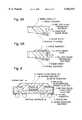
- FIG. 3there is shown a diagrammatic sectional view of a first embodiment of the semiconductor device package in accordance with the present invention.
- a semiconductor device chip 7is mounted at a center zone of an upper surface of a rectangular circuit substrate 1 by action of a bonding agent 9.
- a plurality of wiring conductors 2are formed on a peripheral zone of the upper surface of the circuit substrate 1, and are electrically connected to the semiconductor device chip 7 by means of bonding wires 8.
- a cavity 1A for accommodating the semiconductor device chip 7can be preferably formed at the center zone of the upper surface of the circuit substrate 1, as shown in FIG. 3.
- the semiconductor device chip 7 mounted on the circuit substrate 1is encapsulated with an encapsulating resin 10, which is conventionally an epoxy resin, a phenolic resin, or a silicone resin.
- the circuit substrate 1is formed of an organic wiring substrate material such as a glass-epoxy, a modified polyimide, but can be effectively formed of a ceramic substrate.
- End-face halved through-holes 3in the form obtained by axially halving a through hole along its center axis, are formed at a predetermined constant pitch at each of four end faces of the rectangular circuit substrate 1.
- An inner side surface of the end-face halved through-holes 3are coated with a conductor film 3A extending from an upper end to a lower end of the end-face halved through-hole 3.
- the conductor film 3Ais connected, at the upper end of the end-face halved through-holes 3, to a corresponding one of the wiring conductors 2 formed on the upper surface of the circuit substrate 1, and at the lower end of the end-face halved through-hole 3, to a corresponding one of external electrodes 5 formed on a lower surface of the circuit substrate 1.
- a solder resist 4is applied to cover the external electrode 5 between the lower end of the end-face halved through-hole 3 and an inner end of the external electrode 5, in order to separate the lower end of the end-face halved through-hole 3 from the inner end of the external electrode 5, thereby to prevent a solder applied between the inner end of the external electrodes and for example a printed circuit board when the package is mounted on the printed circuit board, from crawling up on the inside surface of the end-face halved through-holes 3.
- the external electrodes 5are connected to the printed circuit board by means of a solder.
- a solder projection electrode 6 in the form of a bumpcan be formed on the inner end of the external electrode 5.
- the inner end of the external electrodes 5is preferably in the form of a pad.
- the solder resist 4 for separating between the lower end of the end-face halved through-hole 3 and the inner end of the external electrode 5 or the solder projection electrodeis preferably formed of a thermoset or ultraviolet-curing epoxy resin.
- any resin material having a solder masking or repelling effectcan be used.
- the diameter of a through hole for the end-face halved through-hole 3 formed at each end face of the substrateis on the order of 0.2 mm to 0.4 mm.
- the width of a conductor extending from the lower end of the through hole to reach the external electrode 5becomes on the order of 0.3 mm to 0.5 mm, because the conductor extending from the through hole is required to have a width larger than the diameter of the through hole, in order to protect a conductor film coated on the inner surface of the through hole when the through holes are halved by a mechanical cutting tool.
- the pitch of the end-face halved through-holes 3 formed at each end face of the substratebecomes 0.4 mm to 0.8 mm.
- the end-face halved through-holes 3are provided for the purpose of electrically connecting between the conductors respectively formed on the upper surface and the lower surface of the circuit substrate 1, and therefore, it is not preferable that the conductor layer provided on the inside surface of the through hole is disconnected in the process of working the circuit substrate and assembling the package. In order to avoid this inconvenience, it is preferred to previously coat a portion or the whole of the surface of the through hole conductor film with the solder resist. In the prior art LCC type package, since the end-face through-hole electrodes were used as the external electrodes, it was necessary to ensure a solder wettability of the end-face through-hole electrode.
- the present inventionit is no longer necessary to ensure the solder wettability of the end-face through-hole electrode since the end-face through-hole electrodes are not used as the external electrodes, and therefore, the inner surface of the through hole conductor film can be protected with a resin, in order to prevent disconnection of the through hole conductor film.
- FIG. 4there is shown a diagrammatic partial sectional view of a second embodiment of the semiconductor device package in accordance with the present invention.
- elements corresponding to those shown in FIG. 3are given the same Reference Numerals, and explanation thereof will be omitted for simplification of the description.
- a circuit substrate 1afurther includes a plurality of inside-area through-holes 11 formed in the circuit substrate 1a other than the end face region of the circuit substrate, a plurality of additional wiring conductor 22 formed on the upper surface of the circuit substrate 1a and connected to an upper end of the inside-area through-holes 11 and connected to the semiconductor device chip 7 through bonding wire 88, a plurality of additional external electrode 55 formed on the lower surface of the circuit substrate 1 and connected to a lower end of the inside-area through-holes 11, and a solder resist 44 applied to cover the additional external electrode 55 between the lower end of the inside-area through hole 11 and an inner end of the additional external electrode 55, in order to separate between the lower end of the inside-area through hole 11 and an inner end of the additional external electrode 55.
- a solder projection electrode 66 in the form of a bumpcan be formed on the inner end of the external electrode 55.
- the pitch of the end-face halved through-holes 3 formed on each end face of the circuit substrate 1acan be made to 0.5 mm. Therefore, considering the package of 20 mm square, about 140 end-face halved through-holes 3 can be formed.
- the inside-area through holes 11are located at a pitch of 1.27 mm to constitute a matrix of 12 rows and 12 columns, 144 inside-area through holes 11 can be formed. Therefore, 280 or more vias can be formed in total.
- the pitch of 1.27 mmis required for ensuring that at least one conductor passes between adjacent inside-area through holes 11 to constitute a wiring circuit on or in the circuit substrate.
- the viasare constituted of only the inside-area through holes 11, even if the inside-area through holes 11 are located at a pitch of 1.27 mm to constitute a matrix of 14 rows and 14 columns, only 196 vias for interconnecting between the conductors respectively formed on the upper surface and the lower surface of the circuit substrate can be formed. Therefore, by utilizing both the end-face halved through-holes 3 and the inside-area through holes 11, the number of formable vias can be remarkably increased, and therefore, the degree of freedom in design can be elevated.
- FIGS. 5A and 5Bthere are diagrammatic partial sectional views illustrating the end-face halved through-hole of the semiconductor device package in accordance with the present invention.
- FIG. 5Aillustrates the end-face halved through-hole 3 having a lower half coated with the solder resist
- FIG. 5Billustrates the end-face halved through-hole 3 having the whole surface coated with the solder resist.
- a basic purpose of the provision of the solder resist 4is to separate the external electrode 5 and the conductor film 3A formed on the inner side surface of the end-face halved through-hole 3 from each other by the solder resist 4 so as to prevent the external electrode 5 and the end-face halved through-hole conductor film 3A from being simultaneously wetted by the solder. Therefore, it is sufficient if the lower half of the end-face halved through-hole conductor film 3A is covered with a crawled-up solder resist 4a as shown in FIG. 5A. However, the whole surface of the end-face halved through-hole conductor film 3A can be more preferably completely covered with a solder resist cover 4b as shown in FIG. 5B.
- the portion or the whole surface of the end-face halved through-hole conductor film 3Ais covered with the solder resist 4, it becomes easy to cut out the circuit substrate along the through holes for the end-face halved through-holes 3, and simultaneously, an effect of protecting the conductor film exposed at the end face of the package can be obtained.
- the coating of the solder resistcan be carried out by covering the through holes with the solder resist by use of a mask pattern, in the process of manufacturing the circuit substrate.
- FIG. 6is a diagrammatic sectional view of the third embodiment.
- the third embodiment of the semiconductor device package in accordance with the present inventionuses a multilevel ceramic substrate 1b, which internally includes internal conductors 2b in the inside of the substrate, and has wiring conductors 2d, external electrodes 5b and end-face halved through-holes 3 provided on an outer surface of the substrate.
- a semiconductor device chip 7bis mounted on a cavity formed on a center region of an upper surface of the substrate 1b, and is electrically connected through bonding wires 8b to the wiring conductors 2d, and is also encapsulated with a resin 10b.
- the multilevel ceramic substrate 1bis formed of a substrate material mainly composed of alumina (aluminum oxide) or aluminum nitride, and the internal conductors are formed of a refractory metal such as tungsten or molybdenum.
- a glass-ceramic formed by adding glass into aluminacan be used.
- a solder dam 4cis formed to separate the end-face halved through-hole 3 from an inner end of the external electrode 5b.
- the solder dam 4ccan be formed by supplying a material similar to that of the ceramic substrate and then sintering the material, or alternatively by printing a patterned epoxy resin and then curing the patterned epoxy resin.
- the semiconductor device package thus formedcan be mounted on for example a printed circuit board while maintaining the external conductors 5b in a flat conductor condition. However, the semiconductor device package can be mounted after previously forming a solder projection electrode 6b in the form of a bump on the external conductors 5b.
- the semiconductor device package in accordance with the present inventionsince a side surface of the end-face halved through-holes is not used as an electrically connecting external contact face, and since the external electrodes are formed on the other surface of the circuit substrate and connected to the end-face halved through-holes, and furthermore, since the circuit substrate at the outside of the end-face halved through-holes is cut off or removed, the package can be made small.
- the viasare concentrated at the end-face of the substrate, an occupying area per one via becomes small, with the result that a space used for laying out the conductors within the same circuit substrate becomes large, and therefore, the degree of freedom in designing the conductor patter layout can be elevated.
- the number of viascan be remarkably increased.
- the conductor protecting layerseparates the end of the external electrodes from the end-face halved through-holes or the inside-area through-holes, the solder is prevented from crawling up.
- the conductor protecting layersolder resist
Landscapes
- Engineering & Computer Science (AREA)
- Microelectronics & Electronic Packaging (AREA)
- Physics & Mathematics (AREA)
- Condensed Matter Physics & Semiconductors (AREA)
- General Physics & Mathematics (AREA)
- Computer Hardware Design (AREA)
- Power Engineering (AREA)
- Manufacturing & Machinery (AREA)
- Printing Elements For Providing Electric Connections Between Printed Circuits (AREA)
- Non-Metallic Protective Coatings For Printed Circuits (AREA)
- Production Of Multi-Layered Print Wiring Board (AREA)
- Wire Bonding (AREA)
Abstract
Description
Claims (10)
Applications Claiming Priority (2)
| Application Number | Priority Date | Filing Date | Title |
|---|---|---|---|
| JP9080003AJP2976917B2 (en) | 1997-03-31 | 1997-03-31 | Semiconductor device |
| JP9-080003 | 1997-03-31 |
Publications (1)
| Publication Number | Publication Date |
|---|---|
| US5962917Atrue US5962917A (en) | 1999-10-05 |
Family
ID=13706170
Family Applications (1)
| Application Number | Title | Priority Date | Filing Date |
|---|---|---|---|
| US09/050,940Expired - Fee RelatedUS5962917A (en) | 1997-03-31 | 1998-03-31 | Semiconductor device package having end-face halved through-holes and inside-area through-holes |
Country Status (3)
| Country | Link |
|---|---|
| US (1) | US5962917A (en) |
| JP (1) | JP2976917B2 (en) |
| CN (1) | CN1198009A (en) |
Cited By (32)
| Publication number | Priority date | Publication date | Assignee | Title |
|---|---|---|---|---|
| EP0996172A1 (en)* | 1998-10-23 | 2000-04-26 | Rohm Co., Ltd. | Chip type semiconductor light emitting device |
| US6204559B1 (en)* | 1999-11-22 | 2001-03-20 | Advanced Semiconductor Engineering, Inc. | Ball grid assembly type semiconductor package having improved chip edge support to prevent chip cracking |
| US6215184B1 (en)* | 1998-02-19 | 2001-04-10 | Texas Instruments Incorporated | Optimized circuit design layout for high performance ball grid array packages |
| KR20010051976A (en)* | 1999-11-30 | 2001-06-25 | 가네꼬 히사시 | Semiconductor device manufactured by package group molding and dicing method |
| US6262481B1 (en)* | 2000-02-28 | 2001-07-17 | Harvatek Corporation | Folded heat sink for semiconductor device package |
| US6369331B1 (en)* | 1999-09-01 | 2002-04-09 | Fujitsu Limited | Printed circuit board for semiconductor package and method of making same |
| US6372540B1 (en) | 2000-04-27 | 2002-04-16 | Amkor Technology, Inc. | Moisture-resistant integrated circuit chip package and method |
| US6407458B1 (en)* | 2000-05-04 | 2002-06-18 | Amkor Technology, Inc. | Moisture-resistant integrated circuit chip package and method |
| US20020113296A1 (en)* | 2001-02-03 | 2002-08-22 | Samsung Electronics Co., Ltd. | Wafer level hermetic sealing method |
| US6444499B1 (en)* | 2000-03-30 | 2002-09-03 | Amkor Technology, Inc. | Method for fabricating a snapable multi-package array substrate, snapable multi-package array and snapable packaged electronic components |
| US6476331B1 (en) | 2000-06-19 | 2002-11-05 | Amkor Technology, Inc. | Printed circuit board for semiconductor package and method for manufacturing the same |
| US20030117784A1 (en)* | 2001-12-05 | 2003-06-26 | Kenji Fukunabe | Circuit board device and mounting method therefor |
| US6608375B2 (en)* | 2001-04-06 | 2003-08-19 | Oki Electric Industry Co., Ltd. | Semiconductor apparatus with decoupling capacitor |
| US6627482B2 (en)* | 2001-02-09 | 2003-09-30 | Harvatek Corporation | Mass production technique for surface mount optical device with a focusing cup |
| US20030227025A1 (en)* | 2002-04-26 | 2003-12-11 | Matsushita Electric Industrial Co., Ltd. | Electronic circuit device |
| US6683790B1 (en)* | 1999-06-30 | 2004-01-27 | Murata Manufacturing Co., Ltd. | Electronic part, dielectric filter, dielectric duplexer, and manufacturing method of the electronic part |
| US20040048421A1 (en)* | 2000-02-17 | 2004-03-11 | Takashi Noguchi | Method of encapsulating conductive lines of semiconductor devices |
| US6745463B1 (en)* | 2000-10-24 | 2004-06-08 | Unitech Printed Circuit Board Corp. | Manufacturing method of rigid flexible printed circuit board |
| US20040251828A1 (en)* | 2003-04-14 | 2004-12-16 | Toyoda Gosei Co., Ltd. | LED lamp and method for manufacturing the same |
| US20050006734A1 (en)* | 2003-07-07 | 2005-01-13 | Fuaida Harun | Bonding pad for a packaged integrated circuit |
| US20050045371A1 (en)* | 2000-01-25 | 2005-03-03 | Shota Iwasaki | Circuit board |
| US20050070050A1 (en)* | 2003-09-25 | 2005-03-31 | Minami Co., Ltd. | Method of mounting wafer on printed wiring substrate |
| US20050168960A1 (en)* | 2004-01-30 | 2005-08-04 | Toshiyuki Asahi | Module with a built-in component, and electronic device with the same |
| US20060231935A1 (en)* | 2005-04-13 | 2006-10-19 | Nec Electronics Corporation | BGA type semiconductor package featuring additional flat electrode teminals, and method for manufacturing the same |
| US20070166884A1 (en)* | 2005-12-29 | 2007-07-19 | Siliconware Precision Industries Co., Ltd. | Circuit board and package structure thereof |
| US20080048299A1 (en)* | 2001-04-25 | 2008-02-28 | Infineon Technologies Ag | Electronic Component with Semiconductor Chips, Electronic Assembly Composed of Stacked Semiconductor Chips, and Methods for Producing an Electronic Component and an Electronic Assembly |
| US20100015760A1 (en)* | 2001-06-07 | 2010-01-21 | Renesas Technology Corp. | Semiconductor device and manufacturing method thereof |
| US20110121365A1 (en)* | 2001-02-06 | 2011-05-26 | Renesas Electronics Corporation | Hybrid integrated circuit device, and method for fabricating the same, and electronic device |
| US9006585B2 (en)* | 2009-05-19 | 2015-04-14 | Rubycon Corporation | Device for surface mounting and capacitor element |
| US20160360619A1 (en)* | 2015-06-02 | 2016-12-08 | Yageo Corporation | Passive device |
| EP2447993B1 (en)* | 2009-08-21 | 2018-12-19 | Huawei Device (Dongguan) Co., Ltd. | Electronic packaging structure |
| US20230413453A1 (en)* | 2021-03-03 | 2023-12-21 | Stemco Co., Ltd. | Circuit board and method for manufacturing same, and electronic device comprising same circuit board |
Families Citing this family (4)
| Publication number | Priority date | Publication date | Assignee | Title |
|---|---|---|---|---|
| CN100431140C (en)* | 2002-03-21 | 2008-11-05 | Nxp股份有限公司 | Semiconductor device with protective security coating and method of manufacturing the same |
| JP5777481B2 (en)* | 2010-10-18 | 2015-09-09 | 京セラ株式会社 | Light emitting element mounting substrate and light emitting device |
| CN113178395B (en)* | 2021-04-28 | 2023-06-13 | 浙江集迈科微电子有限公司 | Interlayer interconnection process of multi-layer stacked modules |
| CN113423173B (en)* | 2021-05-29 | 2023-09-29 | 华为技术有限公司 | Electronic component packages, electronic component packaging components and electronic equipment |
Citations (12)
| Publication number | Priority date | Publication date | Assignee | Title |
|---|---|---|---|---|
| US2971138A (en)* | 1959-05-18 | 1961-02-07 | Rca Corp | Circuit microelement |
| JPS6153746A (en)* | 1984-08-24 | 1986-03-17 | Hitachi Ltd | Semiconductor device |
| US4691225A (en)* | 1982-02-05 | 1987-09-01 | Hitachi, Ltd. | Semiconductor device and a method of producing the same |
| JPH0282557A (en)* | 1988-09-19 | 1990-03-23 | Matsushita Electron Corp | Semiconductor device |
| JPH0513611A (en)* | 1991-07-05 | 1993-01-22 | Nec Corp | Leadless chip carrier type hybrid ic |
| US5216278A (en)* | 1990-12-04 | 1993-06-01 | Motorola, Inc. | Semiconductor device having a pad array carrier package |
| US5241133A (en)* | 1990-12-21 | 1993-08-31 | Motorola, Inc. | Leadless pad array chip carrier |
| JPH05327157A (en)* | 1992-05-25 | 1993-12-10 | Matsushita Electric Ind Co Ltd | Ceramic substrate |
| JPH05335438A (en)* | 1992-06-04 | 1993-12-17 | Nec Corp | Leadless chip carrier |
| JPH05335437A (en)* | 1992-06-04 | 1993-12-17 | Nec Corp | Semiconductor device |
| US5729437A (en)* | 1994-06-22 | 1998-03-17 | Seiko Epson Corporation | Electronic part including a thin body of molding resin |
| US5796170A (en)* | 1996-02-15 | 1998-08-18 | Northern Telecom Limited | Ball grid array (BGA) integrated circuit packages |
- 1997
- 1997-03-31JPJP9080003Apatent/JP2976917B2/ennot_activeExpired - Fee Related
- 1998
- 1998-03-31USUS09/050,940patent/US5962917A/ennot_activeExpired - Fee Related
- 1998-03-31CNCN98100988Apatent/CN1198009A/enactivePending
Patent Citations (12)
| Publication number | Priority date | Publication date | Assignee | Title |
|---|---|---|---|---|
| US2971138A (en)* | 1959-05-18 | 1961-02-07 | Rca Corp | Circuit microelement |
| US4691225A (en)* | 1982-02-05 | 1987-09-01 | Hitachi, Ltd. | Semiconductor device and a method of producing the same |
| JPS6153746A (en)* | 1984-08-24 | 1986-03-17 | Hitachi Ltd | Semiconductor device |
| JPH0282557A (en)* | 1988-09-19 | 1990-03-23 | Matsushita Electron Corp | Semiconductor device |
| US5216278A (en)* | 1990-12-04 | 1993-06-01 | Motorola, Inc. | Semiconductor device having a pad array carrier package |
| US5241133A (en)* | 1990-12-21 | 1993-08-31 | Motorola, Inc. | Leadless pad array chip carrier |
| JPH0513611A (en)* | 1991-07-05 | 1993-01-22 | Nec Corp | Leadless chip carrier type hybrid ic |
| JPH05327157A (en)* | 1992-05-25 | 1993-12-10 | Matsushita Electric Ind Co Ltd | Ceramic substrate |
| JPH05335438A (en)* | 1992-06-04 | 1993-12-17 | Nec Corp | Leadless chip carrier |
| JPH05335437A (en)* | 1992-06-04 | 1993-12-17 | Nec Corp | Semiconductor device |
| US5729437A (en)* | 1994-06-22 | 1998-03-17 | Seiko Epson Corporation | Electronic part including a thin body of molding resin |
| US5796170A (en)* | 1996-02-15 | 1998-08-18 | Northern Telecom Limited | Ball grid array (BGA) integrated circuit packages |
Cited By (64)
| Publication number | Priority date | Publication date | Assignee | Title |
|---|---|---|---|---|
| US6215184B1 (en)* | 1998-02-19 | 2001-04-10 | Texas Instruments Incorporated | Optimized circuit design layout for high performance ball grid array packages |
| US6180962B1 (en) | 1998-10-23 | 2001-01-30 | Rohm Co., Ltd. | Chip type semiconductor light emitting device having a solder preventive portion |
| EP0996172A1 (en)* | 1998-10-23 | 2000-04-26 | Rohm Co., Ltd. | Chip type semiconductor light emitting device |
| US6683790B1 (en)* | 1999-06-30 | 2004-01-27 | Murata Manufacturing Co., Ltd. | Electronic part, dielectric filter, dielectric duplexer, and manufacturing method of the electronic part |
| US6369331B1 (en)* | 1999-09-01 | 2002-04-09 | Fujitsu Limited | Printed circuit board for semiconductor package and method of making same |
| US6204559B1 (en)* | 1999-11-22 | 2001-03-20 | Advanced Semiconductor Engineering, Inc. | Ball grid assembly type semiconductor package having improved chip edge support to prevent chip cracking |
| KR20010051976A (en)* | 1999-11-30 | 2001-06-25 | 가네꼬 히사시 | Semiconductor device manufactured by package group molding and dicing method |
| US7253363B2 (en)* | 2000-01-25 | 2007-08-07 | Nec Electronics Corporation | Circuit board |
| US20050045371A1 (en)* | 2000-01-25 | 2005-03-03 | Shota Iwasaki | Circuit board |
| US6707166B1 (en)* | 2000-02-17 | 2004-03-16 | Oki Electric Industry Co., Ltd. | Semiconductor devices and manufacturing method thereof |
| US6780671B2 (en) | 2000-02-17 | 2004-08-24 | Oki Electric Industry Co., Ltd. | Method of encapsulating conductive lines of semiconductor devices |
| US20040048421A1 (en)* | 2000-02-17 | 2004-03-11 | Takashi Noguchi | Method of encapsulating conductive lines of semiconductor devices |
| US6262481B1 (en)* | 2000-02-28 | 2001-07-17 | Harvatek Corporation | Folded heat sink for semiconductor device package |
| US6444499B1 (en)* | 2000-03-30 | 2002-09-03 | Amkor Technology, Inc. | Method for fabricating a snapable multi-package array substrate, snapable multi-package array and snapable packaged electronic components |
| US6372540B1 (en) | 2000-04-27 | 2002-04-16 | Amkor Technology, Inc. | Moisture-resistant integrated circuit chip package and method |
| US6407458B1 (en)* | 2000-05-04 | 2002-06-18 | Amkor Technology, Inc. | Moisture-resistant integrated circuit chip package and method |
| US6476331B1 (en) | 2000-06-19 | 2002-11-05 | Amkor Technology, Inc. | Printed circuit board for semiconductor package and method for manufacturing the same |
| US6745463B1 (en)* | 2000-10-24 | 2004-06-08 | Unitech Printed Circuit Board Corp. | Manufacturing method of rigid flexible printed circuit board |
| US6969639B2 (en)* | 2001-02-03 | 2005-11-29 | Samsung Electronics Co., Ltd. | Wafer level hermetic sealing method |
| US20020113296A1 (en)* | 2001-02-03 | 2002-08-22 | Samsung Electronics Co., Ltd. | Wafer level hermetic sealing method |
| US8084852B2 (en) | 2001-02-06 | 2011-12-27 | Renesas Electronics Corporation | Hybrid integrated circuit device, and method for fabricating the same, and electronic device |
| US8581395B2 (en) | 2001-02-06 | 2013-11-12 | Renesas Electronics Corporation | Hybrid integrated circuit device and electronic device |
| US20110121365A1 (en)* | 2001-02-06 | 2011-05-26 | Renesas Electronics Corporation | Hybrid integrated circuit device, and method for fabricating the same, and electronic device |
| US8222734B2 (en) | 2001-02-06 | 2012-07-17 | Renesas Electronics Corporation | Hybrid integrated circuit device and electronic device |
| US6627482B2 (en)* | 2001-02-09 | 2003-09-30 | Harvatek Corporation | Mass production technique for surface mount optical device with a focusing cup |
| US8018055B2 (en) | 2001-04-06 | 2011-09-13 | Oki Electric Industry Co., Ltd. | Semiconductor apparatus with decoupling capacitor |
| US6608375B2 (en)* | 2001-04-06 | 2003-08-19 | Oki Electric Industry Co., Ltd. | Semiconductor apparatus with decoupling capacitor |
| US6806564B2 (en) | 2001-04-06 | 2004-10-19 | Oki Electric Industry Co., Ltd. | Semiconductor apparatus with decoupling capacitor |
| US20100207244A1 (en)* | 2001-04-06 | 2010-08-19 | Oki Electric Industry Co., Ltd. | Semiconductor apparatus with decoupling capacitor |
| US7714434B2 (en) | 2001-04-06 | 2010-05-11 | Oki Electric Industry Co., Ltd. | Semiconductor apparatus with decoupling capacitor |
| US20090096063A1 (en)* | 2001-04-06 | 2009-04-16 | Oki Electric Industry Co., Ltd. | Semiconductor apparatus with decoupling capacitor |
| US7459765B2 (en) | 2001-04-06 | 2008-12-02 | Oki Electric Industry Co., Ltd. | Semiconductor apparatus with decoupling capacitor |
| US7173335B2 (en) | 2001-04-06 | 2007-02-06 | Oki Electric Industry Co., Ltd. | Semiconductor apparatus with decoupling capacitor |
| US20040145041A1 (en)* | 2001-04-06 | 2004-07-29 | Makoto Terui | Semiconductor apparatus with decoupling capacitor |
| US8350364B2 (en) | 2001-04-25 | 2013-01-08 | Qimonda Ag | Electronic component with semiconductor chips, electronic assembly composed of stacked semiconductor chips, and methods for producing an electronic component and an electronic assembly |
| US20080048299A1 (en)* | 2001-04-25 | 2008-02-28 | Infineon Technologies Ag | Electronic Component with Semiconductor Chips, Electronic Assembly Composed of Stacked Semiconductor Chips, and Methods for Producing an Electronic Component and an Electronic Assembly |
| US7342320B2 (en)* | 2001-04-25 | 2008-03-11 | Infineon Technologies Ag | Electronic component with semiconductor chips, electronic assembly composed of stacked semiconductor chips, and methods for producing an electronic component and an electronic assembly |
| US20110171780A1 (en)* | 2001-06-07 | 2011-07-14 | Renesas Electronics Corporation | Semiconductor device and manufacturing method thereof |
| US9613922B2 (en) | 2001-06-07 | 2017-04-04 | Renesas Electronics Corporation | Semiconductor device and manufacturing method thereof |
| US8952527B2 (en) | 2001-06-07 | 2015-02-10 | Renesas Electronics Corporation | Semiconductor device and manufacturing method thereof |
| US8653655B2 (en) | 2001-06-07 | 2014-02-18 | Renesas Electronics Corporation | Semiconductor device and manufacturing method thereof |
| US20100015760A1 (en)* | 2001-06-07 | 2010-01-21 | Renesas Technology Corp. | Semiconductor device and manufacturing method thereof |
| US8524534B2 (en) | 2001-06-07 | 2013-09-03 | Renesas Electronics Corporation | Semiconductor device and manufacturing method thereof |
| US8278147B2 (en) | 2001-06-07 | 2012-10-02 | Renesas Electronics Corporation | Semiconductor device and manufacturing method thereof |
| US20030117784A1 (en)* | 2001-12-05 | 2003-06-26 | Kenji Fukunabe | Circuit board device and mounting method therefor |
| US7000312B2 (en)* | 2001-12-05 | 2006-02-21 | Murata Manufacturing Co., Ltd. | Circuit board device and mounting method therefor |
| US20030227025A1 (en)* | 2002-04-26 | 2003-12-11 | Matsushita Electric Industrial Co., Ltd. | Electronic circuit device |
| US7332862B2 (en)* | 2003-04-14 | 2008-02-19 | Toyoda Gosei Co., Ltd. | Led lamp including a resist bonded to a copper film |
| US20040251828A1 (en)* | 2003-04-14 | 2004-12-16 | Toyoda Gosei Co., Ltd. | LED lamp and method for manufacturing the same |
| US20050006734A1 (en)* | 2003-07-07 | 2005-01-13 | Fuaida Harun | Bonding pad for a packaged integrated circuit |
| US7042098B2 (en)* | 2003-07-07 | 2006-05-09 | Freescale Semiconductor,Inc | Bonding pad for a packaged integrated circuit |
| US20060231959A1 (en)* | 2003-07-07 | 2006-10-19 | Fuaida Harun | Bonding pad for a packaged integrated circuit |
| US7141453B2 (en)* | 2003-09-25 | 2006-11-28 | Minami Co., Ltd. | Method of mounting wafer on printed wiring substrate |
| US20050070050A1 (en)* | 2003-09-25 | 2005-03-31 | Minami Co., Ltd. | Method of mounting wafer on printed wiring substrate |
| CN100413386C (en)* | 2003-09-25 | 2008-08-20 | 南株式会社 | Method of mounting wafer on printed wiring substrate |
| US20050168960A1 (en)* | 2004-01-30 | 2005-08-04 | Toshiyuki Asahi | Module with a built-in component, and electronic device with the same |
| US8064213B2 (en) | 2004-01-30 | 2011-11-22 | Panasonic Corporation | Module with a built-in component, and electronic device with the same |
| US20060231935A1 (en)* | 2005-04-13 | 2006-10-19 | Nec Electronics Corporation | BGA type semiconductor package featuring additional flat electrode teminals, and method for manufacturing the same |
| US20070166884A1 (en)* | 2005-12-29 | 2007-07-19 | Siliconware Precision Industries Co., Ltd. | Circuit board and package structure thereof |
| US9006585B2 (en)* | 2009-05-19 | 2015-04-14 | Rubycon Corporation | Device for surface mounting and capacitor element |
| EP2447993B1 (en)* | 2009-08-21 | 2018-12-19 | Huawei Device (Dongguan) Co., Ltd. | Electronic packaging structure |
| US20160360619A1 (en)* | 2015-06-02 | 2016-12-08 | Yageo Corporation | Passive device |
| US20230413453A1 (en)* | 2021-03-03 | 2023-12-21 | Stemco Co., Ltd. | Circuit board and method for manufacturing same, and electronic device comprising same circuit board |
| US12376238B2 (en)* | 2021-03-03 | 2025-07-29 | Stemco Co., Ltd. | Circuit board and method for manufacturing same, and electronic device comprising same circuit board |
Also Published As
| Publication number | Publication date |
|---|---|
| CN1198009A (en) | 1998-11-04 |
| JPH10275875A (en) | 1998-10-13 |
| JP2976917B2 (en) | 1999-11-10 |
Similar Documents
| Publication | Publication Date | Title |
|---|---|---|
| US5962917A (en) | Semiconductor device package having end-face halved through-holes and inside-area through-holes | |
| US12035472B2 (en) | Stackable via package and method | |
| US5796589A (en) | Ball grid array integrated circuit package that has vias located within the solder pads of a package | |
| CN100355064C (en) | Low cost microelectronic circuit package | |
| US6607942B1 (en) | Method of fabricating as grooved heat spreader for stress reduction in an IC package | |
| US6667546B2 (en) | Ball grid array semiconductor package and substrate without power ring or ground ring | |
| US6218731B1 (en) | Tiny ball grid array package | |
| US6084295A (en) | Semiconductor device and circuit board used therein | |
| US5668406A (en) | Semiconductor device having shielding structure made of electrically conductive paste | |
| US5847458A (en) | Semiconductor package and device having heads coupled with insulating material | |
| US20080179737A1 (en) | Semiconductor device | |
| US5773895A (en) | Anchor provisions to prevent mold delamination in an overmolded plastic array package | |
| US7109573B2 (en) | Thermally enhanced component substrate | |
| US5977624A (en) | Semiconductor package and assembly for fabricating the same | |
| US8138608B2 (en) | Integrated circuit package substrate having configurable bond pads | |
| US20080043447A1 (en) | Semiconductor package having laser-embedded terminals | |
| US5691569A (en) | Integrated circuit package that has a plurality of staggered pins | |
| JP2001168233A (en) | Multiple-line grid array package | |
| KR100620875B1 (en) | Semiconductor device to be mounted on main circuit board and process for manufacturing same device | |
| US20020195721A1 (en) | Cavity down ball grid array packaging structure | |
| US6384477B2 (en) | Multiple line grid array package | |
| JPH09326450A (en) | Semiconductor device and manufacturing method thereof | |
| KR19990065599A (en) | Semiconductor package, manufacturing method thereof and lamination method | |
| JP2000082762A (en) | Semiconductor device | |
| US11139228B2 (en) | Semiconductor device |
Legal Events
| Date | Code | Title | Description |
|---|---|---|---|
| AS | Assignment | Owner name:NEC CORPORATION, JAPAN Free format text:ASSIGNMENT OF ASSIGNORS INTEREST;ASSIGNOR:MORIYAMA, YOSHIFUMI;REEL/FRAME:009086/0780 Effective date:19980330 | |
| FEPP | Fee payment procedure | Free format text:PAYER NUMBER DE-ASSIGNED (ORIGINAL EVENT CODE: RMPN); ENTITY STATUS OF PATENT OWNER: LARGE ENTITY Free format text:PAYOR NUMBER ASSIGNED (ORIGINAL EVENT CODE: ASPN); ENTITY STATUS OF PATENT OWNER: LARGE ENTITY | |
| FEPP | Fee payment procedure | Free format text:PAYOR NUMBER ASSIGNED (ORIGINAL EVENT CODE: ASPN); ENTITY STATUS OF PATENT OWNER: LARGE ENTITY | |
| AS | Assignment | Owner name:NEC ELECTRONICS CORPORATION, JAPAN Free format text:ASSIGNMENT OF ASSIGNORS INTEREST;ASSIGNOR:NEC CORPORATION;REEL/FRAME:013755/0392 Effective date:20021101 | |
| FPAY | Fee payment | Year of fee payment:4 | |
| REMI | Maintenance fee reminder mailed | ||
| LAPS | Lapse for failure to pay maintenance fees | ||
| LAPS | Lapse for failure to pay maintenance fees | Free format text:PATENT EXPIRED FOR FAILURE TO PAY MAINTENANCE FEES (ORIGINAL EVENT CODE: EXP.); ENTITY STATUS OF PATENT OWNER: LARGE ENTITY | |
| STCH | Information on status: patent discontinuation | Free format text:PATENT EXPIRED DUE TO NONPAYMENT OF MAINTENANCE FEES UNDER 37 CFR 1.362 | |
| FP | Lapsed due to failure to pay maintenance fee | Effective date:20071005 |