US5962081A - Method for the manufacture of a membrane-containing microstructure - Google Patents
Method for the manufacture of a membrane-containing microstructureDownload PDFInfo
- Publication number
- US5962081A US5962081AUS08/945,855US94585597AUS5962081AUS 5962081 AUS5962081 AUS 5962081AUS 94585597 AUS94585597 AUS 94585597AUS 5962081 AUS5962081 AUS 5962081A
- Authority
- US
- United States
- Prior art keywords
- hole
- membrane
- substrate body
- layer
- polymer
- Prior art date
- Legal status (The legal status is an assumption and is not a legal conclusion. Google has not performed a legal analysis and makes no representation as to the accuracy of the status listed.)
- Expired - Lifetime
Links
Images


Classifications
- F—MECHANICAL ENGINEERING; LIGHTING; HEATING; WEAPONS; BLASTING
- F04—POSITIVE - DISPLACEMENT MACHINES FOR LIQUIDS; PUMPS FOR LIQUIDS OR ELASTIC FLUIDS
- F04B—POSITIVE-DISPLACEMENT MACHINES FOR LIQUIDS; PUMPS
- F04B43/00—Machines, pumps, or pumping installations having flexible working members
- F04B43/02—Machines, pumps, or pumping installations having flexible working members having plate-like flexible members, e.g. diaphragms
- F04B43/04—Pumps having electric drive
- F04B43/043—Micropumps
- F—MECHANICAL ENGINEERING; LIGHTING; HEATING; WEAPONS; BLASTING
- F15—FLUID-PRESSURE ACTUATORS; HYDRAULICS OR PNEUMATICS IN GENERAL
- F15C—FLUID-CIRCUIT ELEMENTS PREDOMINANTLY USED FOR COMPUTING OR CONTROL PURPOSES
- F15C5/00—Manufacture of fluid circuit elements; Manufacture of assemblages of such elements integrated circuits
Definitions
- the present inventionrelates to a novel method for manufacturing a microstructure comprising an elastic membrane.
- WO 90/05295discloses an optical biosensor system wherein a sample solution containing biomolecules is passed over a sensing surface having immobilized thereon ligands specific for the biomolecules. Binding of the biomolecules to the sensing surface of a sensor chip is detected by surface plasmon resonance spectroscopy (SPRS).
- SPRSsurface plasmon resonance spectroscopy
- a microfluidic systemcomprising channels and valves supplies a controlled sample flow to the sensor surface, allowing real time kinetic analysis at the sensor surface.
- the microfluidic systemis based upon pneumatically controlled valves with a thin elastomer as membrane and comprises two assembled plates, e.g. of plastic, one of the plates having fluid channels formed by high precision moulding in an elastomer layer, such as silicone rubber, applied to one face thereof.
- the other platehas air channels for pneumatic actuation formed therein which are separated from the fluid channels in the other plate by an elastomer membrane, such as silicone rubber, applied to the plate surface.
- the integrated valves formedhave a low dead volume, low pressure drop and a large opening gap minimizing particle problems.
- Such a microfluidic system constructed from polystyrene and siliconeis included in a commercial biosensor system, BIAcoreTM, marketed by Pharmacia Biosensor AB, Uppsala, Sweden.
- Elderstig, H., et al., Sensors and Actuators A46: 95-97, 1995discloses the manufacture of a capacitive pressure sensor by surface micromachining.
- a substrate having a silicon oxide layer and a superposed silicon nitride layerOn a substrate having a silicon oxide layer and a superposed silicon nitride layer, a continuous cavity is etched in the oxide layer through a large amount of small holes in the nitride layer. A polyimide film is then spun on top of the perforated membrane to close the holes.
- the object of the present inventionis to provide a method which simplifies the fabrication of and permits further miniaturization of microfluidic structures as well as other structures comprising a flexible polymer membrane.
- this objectis achieved by integrating a polymer deposition process into a fabrication sequence which comprises micromachining of etchable substrates.
- the substrate bodyis preferably of etchable material and is advantageously plate- or disk-shaped. While silicon is the preferred substrate material, glass or quartz may also be contemplated for the purposes of the invention.
- the substrate bodymay also be a composite material, such as a silicon plate covered by one or more layers of another etchable material or materials, e.g. silicon nitride, silicon dioxide etc.
- Preferred polymer materialsare elastomers, such as silicone rubber and polyimide.
- the formation of the holes or cavitiesis preferably effected by etching, optionally from two sides, but partial or even complete formation of the holes may also be performed by other techniques, such as laser drilling.
- Deposition of the polymer layermay be performed by spin deposition, which is currently preferred, but also other polymer deposition techniques may be contemplated, such as areosol deposition, dip coating etc.
- a membrane support in the form of a sacrificial support layer for the polymermay be required before depositing the polymer, since (i) application of the polymer directly to a completed through-hole or -holes will result in the polymer flowing into and partially filling the hole rather than forming a membrane over it, and (ii) in the case of hole etching, for conventional silicon etching agents, such as KOH and BHF (buffered hydrogen fluoride), a polymer membrane which is applied before the hole etching procedure is completed will lose its adherence to the substrate during the etch.
- a sacrificial support layermay be applied before or after etching the hole or holes.
- the sacrificial support layerWhen the sacrificial support layer is applied before the hole etch, it may be a layer of a material which is not affected by the hole etch, for example a silicon oxide or nitride layer applied to the hole bottom side of the substrate before the etch. After etching of the hole(s) and deposition of the polymer, the sacrificial layer is then selectively etched away.
- the hole bottom side of the substrateis first covered by a protective layer.
- a protective layermay be a layer of a material which is not affected by the hole etch, such as, for example, a silicon oxide or nitride layer, thereby leaving the etched hole or holes covered by this protective layer.
- a selectively removable sacrificial support layer, such as a photoresistis then applied to the open hole side of the substrate, thereby filling the bottom of the holes, whereupon the protective layer is removed and the polymer layer is deposited against the bared substrate face including the filled hole bottom(s). The support layer can then be removed without affecting the adherence of the elastomer layer to the substrate.
- the adherence of the polymer membranemay, on the other hand, not be lost, and the provision of a special sacrificial membrane support layer may therefore not be necessary, but the substrate material itself may serve as membrane support.
- the polymer membrane layeris applied to the substrate and the etching of the hole or holes is then effected up to the polymer membrane.
- Another way of avoiding the use of a sacrificial layeris to etch small pores (of Angstrom size) in the silicon substrate, either only in the regions where the membrane holes are to be etched, or optionally in the whole silicon plate.
- the polymer membraneis then deposited, and the desired holes are etched with a mild etch, such as weak KOH.
- polymer membrane-containing microstructuresBy combining polymer spin deposition methods with semiconductor manufacturing technology as described above, a wide variety of polymer membrane-containing microstructures may be conveniently produced, such as for example, valves, pressure sensors, pumps, semipermeable sensor membranes, etc.
- FIG. 1is a schematic exploded sectional view of one embodiment of a membrane valve
- FIGS. 2A, 2B, 2C, 2D, 2E and 2Fare schematic sectional views of a processed silicon substrate at different stages in one process embodiment for the production of a part of the membrane valve in FIG. 1;
- FIGS. 3A, 3B, 3C and 3Dare schematic partial sectional views of a processed silicon substrate at different stages in a process embodiment for the production of a membrane valve member with a securing groove for the membrane;
- FIGS. 4A, 4B, 4C, 4D, 4E and 4Fare schematic partial sectional views of a processed silicon substrate at different stages in an alternative process embodiment for the production of the membrane valve member in FIG. 1;
- FIGS. 5A and 5Bare schematic partial sectional views of a one-way valve.
- FIGS. 6A and 6Bare schematic partial sectional views of a membrane pump.
- anisotropic etchIn a crystal direction dependent etch in a crystalline material, so-called anisotropic etch, etching is effected up to an atomic plane (111), which gives an extremely smooth surface. In a so-called isotropic etch, on the other hand, the etch is independent of the crystal direction.
- the above-mentioned selectivityis based upon differences in the etch rates between different materials for a particular etching agent.
- etching with hydrogen fluoridetakes place (isotropically) about 1,000 to about 10,000 times faster in silicon dioxide than in silicon.
- sodium hydroxidegives an anisotropic etch of silicon that is about 100 times more efficient than for silicon dioxide, while a mixture of hydrogen fluoride and nitric acid gives a selective isotropic etch of silicon that is about 10 times faster than in silicon dioxide.
- FIG. 1illustrates a membrane valve consisting of three stacked silicon wafers, i.e. an upper silicon wafer 1, a middle silicon wafer 2 and a lower silicon wafer 3.
- the lower wafer 3has a fluid inlet 4 and a fluid outlet 5 connected via a fluid channel 6 with two valve seats 7 interrupting the flow.
- the fluid channel 6may, for example, have a width of about 200 ⁇ m and a depth of about 50 ⁇ m, and the valve seats 7 may have length of about 10 ⁇ m.
- the middle wafer 2covers the fluid channel and has an elastomer layer 8, e.g. silicone rubber, applied to its underside. Right above each valve seat 7, the silicone layer extends over a hole or recess 9 in the wafer such that a free membrane 8a is formed above each valve seat. Recesses 9 are connected via a channel 10.
- an elastomer layer 8e.g. silicone rubber
- the upper wafer 1which also has an elastomer layer 11, e.g. silicone rubber, applied to its underside, functions as a lid and has a bore 12 for connection to an air pressure control means.
- an elastomer layer 11e.g. silicone rubber
- FIGS. 2A to 2FA process sequence for manufacturing the middle wafer 2 is shown in FIGS. 2A to 2F.
- a double-polished silicon wafer 2is oxidized to form an oxide layer 13 thereon. After patterning the air channel 10 (FIG. 1), the oxide layer is etched.
- Silicon nitride depositionis then performed to form a nitride layer 14 as illustrated in FIG. 2B.
- the membrane holes 9(FIG. 1) are patterned and the nitride layer 14 is etched to form a nitride mask with the desired hole pattern.
- a deep anisotropic silicon etchis then effected, e.g. with KOH (30%), through the nitride mask, resulting in partial membrane holes 9', as shown in FIG. 2C.
- a selective silicon etchis performed, e.g. with KOH-IPA, to complete the opening of the membrane holes 9 and simultaneously etch the air channel 10.
- the resulting wafer with only the thin oxide/nitride layers 13, 14 covering the membrane holes 9is illustrated in FIG. 2D.
- the remaining nitride layer 14 on the sides and bottom of the wafer 2is then selectively etched, and a thin layer, for example about 25 ⁇ m thickness, of an elastomer, e.g. a two-component silicone elastomer 15, is applied by spin-deposition.
- an elastomere.g. a two-component silicone elastomer
- the bared oxide 13 at the bottom of holes 9is selectively etched by an agent that does not affect the elastomer 15, such as an RIE plasma etch.
- the completed middle wafer 2is shown in FIG. 2F.
- the upper silicon wafer 1 of the valve in FIG. 1is produced by spin deposition of the elastomer layer 11 to a silicon wafer, and laser boring of the hole 12.
- the lower silicon wafer 3 of the valveis prepared by first oxidizing a silicon wafer, patterning the fluid channel 6, and etching the patterned oxide layer to form an oxide mask with the desired channel pattern. A selective silicon etch is then performed through the oxide mask, e.g. with KOH-IPA, to form the fluid channel 6. After laser drilling of the fluid inlet and outlet holes 4 and 5, fluid channel 6 is oxidized.
- the valveis completed by assembly of the three wafers 1-3 and mounting thereof in a holder (not shown).
- valvesmay be provided in a single silicon wafer.
- the number of valves that may be contained in the wafer, i.e. the packing degree, for the above described silicon etching proceduresis mainly determined by the thickness of the wafer (due to the tapering configuration of the etched holes). For example, with a 200 ⁇ m thick silicon wafer, each valve would occupy an area of at least 0.5 ⁇ 0.5 mm, permitting a packing of up to about 280 valves/cm 2 .
- the attachment of the elastomer membrane to the substrate in the valve areamay be improved by providing a fixing groove for the membrane in the substrate surface, as illustrated in FIGS. 3A to 3D.
- FIG. 3Ashows a silicon wafer 16 with an oxide layer 17 forming a sacrificial membrane 17a over a valve through-hole 18 in the wafer 16.
- An annular edge attachment, or fixing groove,is patterned on the oxide layer 17 around the opening 18, whereupon the bared oxide parts are etched away.
- the siliconis then dry-etched at 19a to a depth of, say, about 10 ⁇ m, as illustrated in FIG. 3B.
- a depth of, say, about 10 ⁇ mBy then subjecting the silicon to an anisotropic KOH etch to a depth of about 10 ⁇ m, negative sides of the etched groove may be obtained.
- FIG. 3Cshows the completed groove 19, which has a width of about twice the depth.
- An elastomer membrane 20, such as silicone rubber,is then spin deposited onto the substrate surface.
- a first deposition at a high rotation speedprovides for good filling of the groove 19, and a subsequent deposition at a low rotation speed gives a smooth surface.
- the sacrificial oxide membraneis then etched away as described previously in connection with FIGS. 2A to 2F.
- FIGS. 4A to 4Fillustrate an alternative way of providing a sacrificial membrane for initially supporting the elastomer membrane.
- a silicon wafer 21is coated with an oxide layer 22 and a superposed nitride layer 23, as shown in FIG. 4A.
- a hole 24is then opened in the upper oxide/nitride layers and the silicon wafer is etched straight through down to the oxide, as illustrated in FIG. 4B.
- a thick layer of positive photoresist 25is then spun onto the etched face of the wafer, partially filling the hole 24 as shown in FIG. 4C.
- the lower oxide/nitride layers 22, 23are subsequently etched away by a dry etch, and the resulting wafer is shown in FIG. 4D.
- the positive photoresist 25is then removed, e.g. with acetone.
- the completed waferis shown in FIG. 4F.
- sacrificial membranes of oxide and photoresisthave been described.
- a combined oxide/nitride sacrificial membranemay be used, i.e. in the process embodiment described above with reference to FIGS. 2A-2F, the nitride need not be etched away before the elastomer deposition.
- a sacrificial membrane structureconsisting of a polysilicon layer sandwiched between two oxide layers and an outer protective nitride layer may be used.
- an etch-resistent metal layermay be used as the sacrificial membrane.
- a major part, say about 3/4, of the depth of holes 9 and 24, respectively,may be preformed by laser-drilling from the top face of the chip, only the remaining hole portion then being etched. Not only will such a procedure speed up the manufacturing procedure to a substantial degree, provided that the number of holes per wafer is relatively low ( ⁇ 1000), but will also permit a still higher packing degree.
- FIGS. 5A and 5BA non-return valve produced by the method of the invention is illustrated in FIGS. 5A and 5B.
- the valveconsists of two silicon plates 27 and 28.
- the lower silicon plate 27has a fluid channel 29 with a valve seat 30 therein.
- the valve seat 30includes a free-etched flexible tongue 31.
- the upper silicon plate 28has an elastomer membrane 32 extending over an etched trough-hole 33 in the plate and may be produced as described above with regard to FIGS. 2A to 2F.
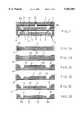
- FIGS. 6A and 6Bshow a membrane pump produced utilizing the method of the invention.
- the pumpconsists of a lower silicon plate 34 having a fluid channel 35 with two valve seats 36 and 37 therein, and an upper silicon plate 38, produced as described above with reference to FIGS. 2A to 2F.
- the upper plate 38comprises three silicone membrane-covered through-holes 39, 40 and 41, each connected to a controlled pressurized air source.
- the membrane-covered holes 39 and 41are located just above the valve seats 36 and 37 to form membrane valves therewith.
- the third membrane-covered hole 40is larger and functions as a fluid actuating member.
- the described membrane pumpwill have a low pressure drop which makes it possible to pump at a high pressure with no leakage in the reverse direction. Since the valves open with a relatively large gap, it will also be possible to pump fairly large particles, which is otherwise a problem with pumps produced by micromachining techniques.
- a silicon wafer of 500 ⁇ m thicknesswas processed by the procedure discussed above in connection with FIGS. 2A to 2F to produce a number of valve plates for use in a membrane valve of the type shown in FIG. 1 as follows.
- the waferwas washed and then oxidized to produce an oxide layer of 1.5 ⁇ m.
- a 1.2 ⁇ m photoresist layerwas then applied to the top face of the wafer, soft-baked for 60 seconds and patterned with a mask corresponding to the desired air channel.
- the photoresistwas then spray developed and hard-baked for 15 min at 110° C.
- the backside of the waferwas then coated with a 1.5 ⁇ m photoresist layer and hard-baked at 110° C. for 10 min.
- the 1.5 ⁇ m oxide layerwas wet-etched by BHF (ammonium buffered hydrogen fluoride), whereupon the photoresist was stripped off.
- BHFammonium buffered hydrogen fluoride
- Nitridewas then deposited to form a 1500 ⁇ nitride layer.
- a 1.5 ⁇ m photoresist layerwas applied to the nitride layer, soft-baked and patterned with a mask corresponding to the membrane holes.
- the photoresistwas spray developed and hard-baked at 110° C. for 20 min.
- the back-side of the waferwas then coated with a 1.5 ⁇ m photoresist layer and hard-baked at 110° C. for 10 min.
- RIEReactive Ion Etch
- a silicon etchwas performed with 30% KOH to a depth of about 420 ⁇ m (etch rate about 1.4 ⁇ m/min).
- 1.5 ⁇ m photoresistwas applied to the back-side of the wafer and hard-baked at 110° C. for 30 min.
- the remaining front nitride layerwas then dry-etched by RIE, followed by dry-stripping of the photoresist with an oxygen plasma at 120° C.
- a short oxide etch with hydrogen fluoride 1:10 for 10 secondswas performed, immediately followed by a silicon etch with KOH/propanol (2 kg KOH, 6.5 l H 2 O, 1.5 l propanol) at 80° C. to a depth of about 100 ⁇ m (etch rate about 1.1 ⁇ m/min), i.e. down to the oxide layer on the back-side of the wafer.
- the nitride on the back-side of the silicon waferwas then etched away, followed by oxidation to 1.5 ⁇ m. After drying at 180° C. for 30 min, a 20 ⁇ m layer of a two-component silicone rubber was applied to the oxide layer on the back-side of the wafer by spin-deposition at 2000 rpm for 40 seconds and then cured at 100° C. for 30 min to form a silicone membrane.
- the oxide layer on the back-side of the waferwas removed by a dry oxide etch through the etched holes in the silicon to bare the silicone membrane.
- the silicon waferwas finally divided into separate valve plates by sawing.
Landscapes
- Engineering & Computer Science (AREA)
- General Engineering & Computer Science (AREA)
- Mechanical Engineering (AREA)
- Computer Hardware Design (AREA)
- Microelectronics & Electronic Packaging (AREA)
- Theoretical Computer Science (AREA)
- Physics & Mathematics (AREA)
- Fluid Mechanics (AREA)
- Micromachines (AREA)
- Separation Using Semi-Permeable Membranes (AREA)
- Immobilizing And Processing Of Enzymes And Microorganisms (AREA)
Abstract
Description
Claims (18)
Applications Claiming Priority (3)
| Application Number | Priority Date | Filing Date | Title |
|---|---|---|---|
| SE9502258 | 1995-06-21 | ||
| SE9502258ASE9502258D0 (en) | 1995-06-21 | 1995-06-21 | Method for the manufacture of a membrane-containing microstructure |
| PCT/SE1996/000789WO1997001055A1 (en) | 1995-06-21 | 1996-06-17 | Method for the manufacture of a membrane-containing microstructure |
Publications (1)
| Publication Number | Publication Date |
|---|---|
| US5962081Atrue US5962081A (en) | 1999-10-05 |
Family
ID=20398698
Family Applications (1)
| Application Number | Title | Priority Date | Filing Date |
|---|---|---|---|
| US08/945,855Expired - LifetimeUS5962081A (en) | 1995-06-21 | 1996-06-17 | Method for the manufacture of a membrane-containing microstructure |
Country Status (6)
| Country | Link |
|---|---|
| US (1) | US5962081A (en) |
| EP (1) | EP0838005B1 (en) |
| JP (1) | JPH11508347A (en) |
| DE (1) | DE69621335D1 (en) |
| SE (1) | SE9502258D0 (en) |
| WO (1) | WO1997001055A1 (en) |
Cited By (104)
| Publication number | Priority date | Publication date | Assignee | Title |
|---|---|---|---|---|
| US6033489A (en)* | 1998-05-29 | 2000-03-07 | Fairchild Semiconductor Corp. | Semiconductor substrate and method of making same |
| US6123861A (en)* | 1996-07-02 | 2000-09-26 | Massachusetts Institute Of Technology | Fabrication of microchip drug delivery devices |
| WO2001017797A1 (en)* | 1999-09-10 | 2001-03-15 | Caliper Technologies Corp. | Microfabrication methods and devices |
| US6296452B1 (en)* | 2000-04-28 | 2001-10-02 | Agilent Technologies, Inc. | Microfluidic pumping |
| WO2002018785A1 (en) | 2000-08-31 | 2002-03-07 | Advanced Sensor Technologies | Micro-fluidic system |
| US6379989B1 (en)* | 1998-12-23 | 2002-04-30 | Xerox Corporation | Process for manufacture of microoptomechanical structures |
| US20020072784A1 (en)* | 2000-10-10 | 2002-06-13 | Sheppard Norman F. | Microchip reservoir devices using wireless transmission of power and data |
| US20020104757A1 (en)* | 1997-12-17 | 2002-08-08 | Christian Schmidt | Efficient methods for the analysis of ion channel proteins |
| US6431212B1 (en) | 2000-05-24 | 2002-08-13 | Jon W. Hayenga | Valve for use in microfluidic structures |
| US20020125135A1 (en)* | 1999-12-23 | 2002-09-12 | Helene Derand | Microfluidic surfaces |
| US6455429B1 (en)* | 1998-03-25 | 2002-09-24 | Institut Fur Mikroelektronik Stuttgart | Method of producing large-area membrane masks |
| US6464842B1 (en) | 1999-06-22 | 2002-10-15 | President And Fellows Of Harvard College | Control of solid state dimensional features |
| US20020163642A1 (en)* | 2000-11-16 | 2002-11-07 | Zoval Jim V. | Optical biodiscs with reflective layers |
| US6479311B1 (en) | 2000-11-27 | 2002-11-12 | Microscan Systems, Inc. | Process for manufacturing micromechanical and microoptomechanical structures with pre-applied patterning |
| US6479315B1 (en) | 2000-11-27 | 2002-11-12 | Microscan Systems, Inc. | Process for manufacturing micromechanical and microoptomechanical structures with single crystal silicon exposure step |
| US6491666B1 (en) | 1999-11-17 | 2002-12-10 | Microchips, Inc. | Microfabricated devices for the delivery of molecules into a carrier fluid |
| US20020187260A1 (en)* | 2001-05-30 | 2002-12-12 | Sheppard Norman F. | Conformal coated microchip reservoir devices |
| US20030008412A1 (en)* | 1997-10-10 | 2003-01-09 | Ciphergen Biosystems, Inc. | Plate alignment and sample transfer indicia for a multiwell multiplate stack and method for processing biological/chemical samples using the same |
| US6506620B1 (en) | 2000-11-27 | 2003-01-14 | Microscan Systems Incorporated | Process for manufacturing micromechanical and microoptomechanical structures with backside metalization |
| US20030010808A1 (en)* | 2001-06-28 | 2003-01-16 | Uhland Scott A. | Methods for hermetically sealing microchip reservoir devices |
| WO2002053290A3 (en)* | 2001-01-08 | 2003-02-20 | Harvard College | Valves and pumps for microfluidic systems and method for making microfluidic systems |
| US6527762B1 (en) | 1999-08-18 | 2003-03-04 | Microchips, Inc. | Thermally-activated microchip chemical delivery devices |
| US20030052002A1 (en)* | 1997-12-17 | 2003-03-20 | Horst Vogel | Multiaperture sample positioning and analysis system |
| WO2003024597A1 (en)* | 2001-09-18 | 2003-03-27 | Åmic AB | Microscale fluid handling system |
| US6551838B2 (en) | 2000-03-02 | 2003-04-22 | Microchips, Inc. | Microfabricated devices for the storage and selective exposure of chemicals and devices |
| US6561224B1 (en) | 2002-02-14 | 2003-05-13 | Abbott Laboratories | Microfluidic valve and system therefor |
| US6581899B2 (en) | 2000-06-23 | 2003-06-24 | Micronics, Inc. | Valve for use in microfluidic structures |
| US20030129360A1 (en)* | 2001-12-31 | 2003-07-10 | Helene Derand | Microfluidic device and its manufacture |
| US20030143114A1 (en)* | 1998-12-30 | 2003-07-31 | Per Andersson | Microanalysis device |
| US20030146091A1 (en)* | 1997-12-17 | 2003-08-07 | Horst Vogel | Multiaperture sample positioning and analysis system |
| US20030156763A1 (en)* | 2001-12-31 | 2003-08-21 | Gyros Ab. | Method and arrangement for reducing noise |
| US20030173650A1 (en)* | 2000-05-12 | 2003-09-18 | Olle Larsson | Micro channel in a substrate |
| US20030211012A1 (en)* | 2002-03-31 | 2003-11-13 | Marten Bergstrom | Efficient microfluidic devices |
| US20030213551A1 (en)* | 2002-04-09 | 2003-11-20 | Helene Derand | Microfluidic devices with new inner surfaces |
| US6660648B1 (en)* | 2000-10-02 | 2003-12-09 | Sandia Corporation | Process for manufacture of semipermeable silicon nitride membranes |
| US6663615B1 (en) | 2001-09-04 | 2003-12-16 | The Ohio State University | Dual stage microvalve and method of use |
| US20040013536A1 (en)* | 2001-08-31 | 2004-01-22 | Hower Robert W | Micro-fluidic pump |
| US20040011977A1 (en)* | 2001-08-31 | 2004-01-22 | Hower Robert W | Micro-fluidic valves |
| US6698454B2 (en) | 2000-11-02 | 2004-03-02 | Biacore Ab | Valve integrally associated with microfluidic liquid transport assembly |
| US20040045891A1 (en)* | 2002-09-09 | 2004-03-11 | Teragenics, Inc. | Implementation of microfluidic components in a microfluidic system |
| US20040067051A1 (en)* | 2000-11-23 | 2004-04-08 | Gunnar Kylberg | Device and method for the controlled heating in micro channel systems |
| US6730072B2 (en) | 2000-05-30 | 2004-05-04 | Massachusetts Institute Of Technology | Methods and devices for sealing microchip reservoir devices |
| US20040094733A1 (en)* | 2001-08-31 | 2004-05-20 | Hower Robert W. | Micro-fluidic system |
| US20040104454A1 (en)* | 2002-10-10 | 2004-06-03 | Rohm Co., Ltd. | Semiconductor device and method of producing the same |
| US20040121486A1 (en)* | 2002-08-16 | 2004-06-24 | Uhland Scott A. | Controlled release device and method using electrothermal ablation |
| US6773429B2 (en) | 2000-10-11 | 2004-08-10 | Microchips, Inc. | Microchip reservoir devices and facilitated corrosion of electrodes |
| US6783643B2 (en) | 1999-06-22 | 2004-08-31 | President And Fellows Of Harvard College | Control of solid state dimensional features |
| US6808522B2 (en) | 1999-12-10 | 2004-10-26 | Massachusetts Institute Of Technology | Microchip devices for delivery of molecules and methods of fabrication thereof |
| US20040229386A1 (en)* | 1999-06-22 | 2004-11-18 | President And Fellows Of Harvard College | Controlled fabrication of gaps in electrically conducting structures |
| US20040240034A1 (en)* | 2001-11-30 | 2004-12-02 | Scharf Bruce R. | Diffraction compensation using a patterned reflector |
| US20040245102A1 (en)* | 2002-09-09 | 2004-12-09 | Gilbert John R. | Implementation of microfluidic components, including molecular fractionation devices, in a microfluidic system |
| US20050006224A1 (en)* | 1999-06-22 | 2005-01-13 | President And Fellows Of Harvard College | Pulsed ion beam control of solid state features |
| US20050014306A1 (en)* | 2003-07-15 | 2005-01-20 | Agency For Science, Technology And Research | Micromachined electromechanical device |
| US20050022888A1 (en)* | 2003-07-31 | 2005-02-03 | Agency For Science, Technology And Research | Microfluidics chips and methods of using same |
| US20050023765A1 (en)* | 2002-01-31 | 2005-02-03 | Coombs James Howard | Bio-safety features for optical analysis disc and disc system including same |
| US20050042770A1 (en)* | 2003-05-23 | 2005-02-24 | Gyros Ab | Fluidic functions based on non-wettable surfaces |
| US6875208B2 (en) | 2001-05-31 | 2005-04-05 | Massachusetts Institute Of Technology | Microchip devices with improved reservoir opening |
| US20050072147A1 (en)* | 2000-08-31 | 2005-04-07 | Hower Robert W | Micro-fluidic actuator |
| US20050092662A1 (en)* | 2002-09-09 | 2005-05-05 | Cytonome, Inc. | Implementation of microfluidic components in a microfluidic system |
| WO2004087281A3 (en)* | 2003-03-31 | 2005-06-16 | Cytonome Inc | Implementation of microfluidic components, including molecular fractionation devices, in a microfluidic system |
| US20050141344A1 (en)* | 2003-10-03 | 2005-06-30 | Gyros Ab | Liquid router |
| US20050153434A1 (en)* | 2001-08-28 | 2005-07-14 | Gyros Ab | Retaining microfluidic microcavity and other microfluidic structures |
| US20050179901A1 (en)* | 2002-05-31 | 2005-08-18 | Gyros Ab | Detector arrangement based on surfaces plasmon resonance |
| US20050186685A1 (en)* | 2004-01-17 | 2005-08-25 | Gyros Ab | Protecting agent |
| US20050214442A1 (en)* | 2001-11-27 | 2005-09-29 | Anders Larsson | Surface and its manufacture and uses |
| US6967101B1 (en) | 1999-03-24 | 2005-11-22 | Gyros Ab | Surface and its manufacture and uses |
| US20050277195A1 (en)* | 2002-04-30 | 2005-12-15 | Gyros Ab | Integrated microfluidic device (ea) |
| US6976982B2 (en) | 2001-01-09 | 2005-12-20 | Microchips, Inc. | Flexible microchip devices for ophthalmic and other applications |
| US20050279925A1 (en)* | 2001-03-19 | 2005-12-22 | Per Andersson | Microfluidic system |
| US20060083639A1 (en)* | 2004-10-12 | 2006-04-20 | Industrial Technology Research Institute | PDMS valve-less micro pump structure and method for producing the same |
| US20060105275A1 (en)* | 2004-11-15 | 2006-05-18 | Maloney John M | Fabrication methods and structures for micro-reservoir devices |
| US7067046B2 (en) | 2000-08-04 | 2006-06-27 | Essen Instruments, Inc. | System for rapid chemical activation in high-throughput electrophysiological measurements |
| US7070590B1 (en) | 1996-07-02 | 2006-07-04 | Massachusetts Institute Of Technology | Microchip drug delivery devices |
| US20060159592A1 (en)* | 1998-05-08 | 2006-07-20 | Gyros Patent Ab | Microfluidic device |
| US20060188401A1 (en)* | 2005-02-23 | 2006-08-24 | Karla Robotti | Microfluidic devices with SPR sensing capabilities |
| US20060194273A1 (en)* | 1998-04-27 | 2006-08-31 | Gyros Patent Ab | Microfabricated apparatus for cell based assays |
| US7118711B1 (en)* | 1999-03-05 | 2006-10-10 | Clondiag Chip Technologies Gmbh | Microcolumn reactor |
| US20070080107A1 (en)* | 2005-10-12 | 2007-04-12 | Postech Foundation | Nanoporous membrane and method of fabricating the same |
| CN1331575C (en)* | 2002-09-09 | 2007-08-15 | 塞通诺米公司 | Implementation of Microfluidic Components in Microfluidic Systems |
| US7258838B2 (en) | 1999-06-22 | 2007-08-21 | President And Fellows Of Harvard College | Solid state molecular probe device |
| US7270730B2 (en) | 2000-08-04 | 2007-09-18 | Essen Instruments, Inc. | High-throughput electrophysiological measurement system |
| US20070274863A1 (en)* | 2003-07-25 | 2007-11-29 | Horacio Kido | Fluidic circuits for sample preparation including bio-discs and methods relating thereto |
| US20080060995A1 (en)* | 2006-09-12 | 2008-03-13 | Sean Zhang | Semi-Permeable Membrane |
| US20080076975A1 (en)* | 2005-01-25 | 2008-03-27 | Microchips, Inc. | Method and implantable device with reservoir array for pre-clinical in vivo testing |
| US20080233594A1 (en)* | 2005-01-17 | 2008-09-25 | Gyros Patent Ab | Method For Detecting An At Least Bivalent Analyte Using Two Affinity Reactants |
| US7429354B2 (en) | 2001-03-19 | 2008-09-30 | Gyros Patent Ab | Structural units that define fluidic functions |
| US20080257859A1 (en)* | 2005-04-06 | 2008-10-23 | President And Fellows Of Harvard College | Molecular characterization with carbon nanotube control |
| US20090010819A1 (en)* | 2004-01-17 | 2009-01-08 | Gyros Patent Ab | Versatile flow path |
| US20090017088A1 (en)* | 2007-07-13 | 2009-01-15 | Biotronik Vi Patent Ag | Implant and system of an implant and a excitation device |
| US7488316B2 (en) | 2005-01-25 | 2009-02-10 | Microchips, Inc. | Control of drug release by transient modification of local microenvironments |
| US20090137874A1 (en)* | 2007-11-26 | 2009-05-28 | The Hong Kong Polytechnic University | Polymer Microvalve with actuators and devices |
| US7553393B2 (en) | 2000-01-30 | 2009-06-30 | Gyros Ab | Method for covering a microfluidic assembly |
| US20100055821A1 (en)* | 2008-08-28 | 2010-03-04 | Buehler Johannes | Method for manufacturing an intergrated pressure sensor |
| US7867194B2 (en) | 2004-01-29 | 2011-01-11 | The Charles Stark Draper Laboratory, Inc. | Drug delivery apparatus |
| US7867193B2 (en) | 2004-01-29 | 2011-01-11 | The Charles Stark Draper Laboratory, Inc. | Drug delivery apparatus |
| US20110151578A1 (en)* | 2008-05-16 | 2011-06-23 | President And Fellows Of Harvard College | Valves and other flow control in fluidic systems including microfluidic systems |
| WO2011107157A1 (en)* | 2010-03-05 | 2011-09-09 | Fraunhofer-Gesellschaft zur Förderung der angewandten Forschung e.V. | Valve, layer structure comprising a first and a second valve, micropump and method of producing a valve |
| US8095197B2 (en) | 2003-11-03 | 2012-01-10 | Microchips, Inc. | Medical device for sensing glucose |
| US20140256030A1 (en)* | 2013-03-08 | 2014-09-11 | Taiwan Semiconductor Manufacturing Company, Ltd. | Scalable Biochip and Method for Making |
| US8876795B2 (en) | 2011-02-02 | 2014-11-04 | The Charles Stark Draper Laboratory, Inc. | Drug delivery apparatus |
| US8961902B2 (en) | 2008-04-23 | 2015-02-24 | Bioscale, Inc. | Method and apparatus for analyte processing |
| US9046192B2 (en) | 2007-01-31 | 2015-06-02 | The Charles Stark Draper Laboratory, Inc. | Membrane-based fluid control in microfluidic devices |
| US10620194B2 (en) | 2001-03-19 | 2020-04-14 | Gyros Patent Ab | Characterization of reaction variables |
| US11867320B2 (en) | 2018-03-02 | 2024-01-09 | National Research Council Of Canada | Polymeric microfluidic valve |
Families Citing this family (18)
| Publication number | Priority date | Publication date | Assignee | Title |
|---|---|---|---|---|
| US6612535B1 (en) | 1997-01-24 | 2003-09-02 | California Institute Of Technology | MEMS valve |
| JP3418727B2 (en)* | 2000-04-27 | 2003-06-23 | 独立行政法人産業技術総合研究所 | Micro valve device and method of manufacturing the same |
| US7459127B2 (en) | 2002-02-26 | 2008-12-02 | Siemens Healthcare Diagnostics Inc. | Method and apparatus for precise transfer and manipulation of fluids by centrifugal and/or capillary forces |
| JP2004130442A (en)* | 2002-10-10 | 2004-04-30 | Rohm Co Ltd | Semiconductor device for micromachine |
| US7125711B2 (en) | 2002-12-19 | 2006-10-24 | Bayer Healthcare Llc | Method and apparatus for splitting of specimens into multiple channels of a microfluidic device |
| US7094354B2 (en) | 2002-12-19 | 2006-08-22 | Bayer Healthcare Llc | Method and apparatus for separation of particles in a microfluidic device |
| US6945116B2 (en)* | 2003-03-19 | 2005-09-20 | California Institute Of Technology | Integrated capacitive microfluidic sensors method and apparatus |
| US7435381B2 (en) | 2003-05-29 | 2008-10-14 | Siemens Healthcare Diagnostics Inc. | Packaging of microfluidic devices |
| US7347617B2 (en) | 2003-08-19 | 2008-03-25 | Siemens Healthcare Diagnostics Inc. | Mixing in microfluidic devices |
| WO2007114912A2 (en)* | 2006-03-30 | 2007-10-11 | Wayne State University | Check valve diaphragm micropump |
| JP6498125B2 (en) | 2012-12-21 | 2019-04-10 | マイクロニクス, インコーポレイテッド | Fluid circuit and associated manufacturing method |
| WO2014100743A2 (en) | 2012-12-21 | 2014-06-26 | Micronics, Inc. | Low elasticity films for microfluidic use |
| WO2014100725A1 (en) | 2012-12-21 | 2014-06-26 | Micronics, Inc. | Portable fluorescence detection system and microassay cartridge |
| CA2911303C (en) | 2013-05-07 | 2021-02-16 | Micronics, Inc. | Methods for preparation of nucleic acid-containing samples using clay minerals and alkaline solutions |
| CA2911308C (en) | 2013-05-07 | 2021-10-19 | Micronics, Inc. | Device for preparation and analysis of nucleic acids |
| EP2994750B1 (en) | 2013-05-07 | 2020-08-12 | PerkinElmer Health Sciences, Inc. | Microfluidic devices and methods for performing serum separation and blood cross-matching |
| NL2014801B1 (en)* | 2015-05-13 | 2017-01-27 | Berkin Bv | Fluid flow device, comprising a valve unit, as well as method of manufacturing the same. |
| BR112018007738A2 (en)* | 2015-11-11 | 2018-10-23 | Dana Automotive Systems Group | air joint ventilation system |
Citations (16)
| Publication number | Priority date | Publication date | Assignee | Title |
|---|---|---|---|---|
| US3860448A (en)* | 1973-04-25 | 1975-01-14 | Gen Motors Corp | Method of applying silicone passivants to etch moats in mesa device wafers |
| US3895135A (en)* | 1973-05-01 | 1975-07-15 | Union Carbide Corp | Masking process with constricted flow path for coating |
| US3951701A (en)* | 1974-03-29 | 1976-04-20 | Licentia Patent-Verwaltungs-G.M.B.H. | Mask for use in production of semiconductor arrangements |
| US4103073A (en)* | 1976-01-09 | 1978-07-25 | Dios, Inc. | Microsubstrates and method for making micropattern devices |
| US4536421A (en)* | 1980-08-01 | 1985-08-20 | Hitachi, Ltd. | Method of forming a microscopic pattern |
| US4581624A (en)* | 1984-03-01 | 1986-04-08 | Allied Corporation | Microminiature semiconductor valve |
| US4743462A (en)* | 1986-07-14 | 1988-05-10 | United Technologies Corporation | Method for preventing closure of cooling holes in hollow, air cooled turbine engine components during application of a plasma spray coating |
| US4869282A (en)* | 1988-12-09 | 1989-09-26 | Rosemount Inc. | Micromachined valve with polyimide film diaphragm |
| US4884337A (en)* | 1986-11-26 | 1989-12-05 | Epicor Technology, Inc. | Method for temporarily sealing holes in printed circuit boards utilizing a thermodeformable material |
| US4988403A (en)* | 1988-12-21 | 1991-01-29 | Rohm Co., Ltd. | Method of forming patterned silicone rubber layer |
| US5277929A (en)* | 1990-10-15 | 1994-01-11 | Nippon Cmk Corp. | Method for masking through holes in manufacturing process of printed circuit board |
| US5313264A (en)* | 1988-11-10 | 1994-05-17 | Pharmacia Biosensor Ab | Optical biosensor system |
| US5334342A (en)* | 1991-08-16 | 1994-08-02 | Rockwell International Corporation | Method of fabricating of diamond moth-eye surface |
| SE501713C2 (en)* | 1993-09-06 | 1995-05-02 | Pharmacia Biosensor Ab | Diaphragm-type valve, especially for liquid handling blocks with micro-flow channels |
| US5454928A (en)* | 1994-01-14 | 1995-10-03 | Watkins Johnson Company | Process for forming solid conductive vias in substrates |
| US5658710A (en)* | 1993-07-16 | 1997-08-19 | Adagio Associates, Inc. | Method of making superhard mechanical microstructures |
- 1995
- 1995-06-21SESE9502258Apatent/SE9502258D0/enunknown
- 1996
- 1996-06-17USUS08/945,855patent/US5962081A/ennot_activeExpired - Lifetime
- 1996-06-17WOPCT/SE1996/000789patent/WO1997001055A1/enactiveIP Right Grant
- 1996-06-17DEDE69621335Tpatent/DE69621335D1/ennot_activeExpired - Lifetime
- 1996-06-17JPJP9503781Apatent/JPH11508347A/enactivePending
- 1996-06-17EPEP96921188Apatent/EP0838005B1/ennot_activeExpired - Lifetime
Patent Citations (17)
| Publication number | Priority date | Publication date | Assignee | Title |
|---|---|---|---|---|
| US3860448A (en)* | 1973-04-25 | 1975-01-14 | Gen Motors Corp | Method of applying silicone passivants to etch moats in mesa device wafers |
| US3895135A (en)* | 1973-05-01 | 1975-07-15 | Union Carbide Corp | Masking process with constricted flow path for coating |
| US3951701A (en)* | 1974-03-29 | 1976-04-20 | Licentia Patent-Verwaltungs-G.M.B.H. | Mask for use in production of semiconductor arrangements |
| US4103073A (en)* | 1976-01-09 | 1978-07-25 | Dios, Inc. | Microsubstrates and method for making micropattern devices |
| US4536421A (en)* | 1980-08-01 | 1985-08-20 | Hitachi, Ltd. | Method of forming a microscopic pattern |
| US4581624A (en)* | 1984-03-01 | 1986-04-08 | Allied Corporation | Microminiature semiconductor valve |
| US4743462A (en)* | 1986-07-14 | 1988-05-10 | United Technologies Corporation | Method for preventing closure of cooling holes in hollow, air cooled turbine engine components during application of a plasma spray coating |
| US4884337A (en)* | 1986-11-26 | 1989-12-05 | Epicor Technology, Inc. | Method for temporarily sealing holes in printed circuit boards utilizing a thermodeformable material |
| US5313264A (en)* | 1988-11-10 | 1994-05-17 | Pharmacia Biosensor Ab | Optical biosensor system |
| US4869282A (en)* | 1988-12-09 | 1989-09-26 | Rosemount Inc. | Micromachined valve with polyimide film diaphragm |
| US4988403A (en)* | 1988-12-21 | 1991-01-29 | Rohm Co., Ltd. | Method of forming patterned silicone rubber layer |
| US5277929A (en)* | 1990-10-15 | 1994-01-11 | Nippon Cmk Corp. | Method for masking through holes in manufacturing process of printed circuit board |
| US5334342A (en)* | 1991-08-16 | 1994-08-02 | Rockwell International Corporation | Method of fabricating of diamond moth-eye surface |
| US5593130A (en)* | 1993-06-09 | 1997-01-14 | Pharmacia Biosensor Ab | Valve, especially for fluid handling bodies with microflowchannels |
| US5658710A (en)* | 1993-07-16 | 1997-08-19 | Adagio Associates, Inc. | Method of making superhard mechanical microstructures |
| SE501713C2 (en)* | 1993-09-06 | 1995-05-02 | Pharmacia Biosensor Ab | Diaphragm-type valve, especially for liquid handling blocks with micro-flow channels |
| US5454928A (en)* | 1994-01-14 | 1995-10-03 | Watkins Johnson Company | Process for forming solid conductive vias in substrates |
Non-Patent Citations (2)
| Title |
|---|
| H. Elderstig et al., Sensors and Actuators A 46 47 (1995) 95 97 (no month).* |
| H. Elderstig et al., Sensors and Actuators A 46-47 (1995) 95-97 (no month). |
Cited By (209)
| Publication number | Priority date | Publication date | Assignee | Title |
|---|---|---|---|---|
| US7901397B2 (en) | 1996-07-02 | 2011-03-08 | Massachusetts Institute Of Technology | Method for operating microchip reservoir device |
| US7918842B2 (en) | 1996-07-02 | 2011-04-05 | Massachusetts Institute Of Technology | Medical device with controlled reservoir opening |
| US7070590B1 (en) | 1996-07-02 | 2006-07-04 | Massachusetts Institute Of Technology | Microchip drug delivery devices |
| US20080051766A1 (en)* | 1996-07-02 | 2008-02-28 | Massachusetts Institute Of Technology | Method for Operating Microchip Reservoir Device |
| US6123861A (en)* | 1996-07-02 | 2000-09-26 | Massachusetts Institute Of Technology | Fabrication of microchip drug delivery devices |
| US7892221B2 (en) | 1996-07-02 | 2011-02-22 | Massachusetts Institute Of Technology | Method of controlled drug delivery from implant device |
| US20030008412A1 (en)* | 1997-10-10 | 2003-01-09 | Ciphergen Biosystems, Inc. | Plate alignment and sample transfer indicia for a multiwell multiplate stack and method for processing biological/chemical samples using the same |
| US20030052002A1 (en)* | 1997-12-17 | 2003-03-20 | Horst Vogel | Multiaperture sample positioning and analysis system |
| US20030146091A1 (en)* | 1997-12-17 | 2003-08-07 | Horst Vogel | Multiaperture sample positioning and analysis system |
| US7201836B2 (en) | 1997-12-17 | 2007-04-10 | Molecular Devices Corporation | Multiaperture sample positioning and analysis system |
| US7244349B2 (en) | 1997-12-17 | 2007-07-17 | Molecular Devices Corporation | Multiaperture sample positioning and analysis system |
| US20020104757A1 (en)* | 1997-12-17 | 2002-08-08 | Christian Schmidt | Efficient methods for the analysis of ion channel proteins |
| US7387715B2 (en) | 1997-12-17 | 2008-06-17 | Molecular Devices Corporation | Sample positioning and analysis system |
| US6455429B1 (en)* | 1998-03-25 | 2002-09-24 | Institut Fur Mikroelektronik Stuttgart | Method of producing large-area membrane masks |
| US20060194273A1 (en)* | 1998-04-27 | 2006-08-31 | Gyros Patent Ab | Microfabricated apparatus for cell based assays |
| US7935522B2 (en) | 1998-04-27 | 2011-05-03 | Gyros Patent Ab | Microfabricated apparatus for cell based assays |
| US8030062B2 (en) | 1998-04-27 | 2011-10-04 | Gyros Patent Ab | Microfabricated apparatus for cell based assays |
| US8722421B2 (en) | 1998-05-08 | 2014-05-13 | Gyros Patent Ab | Microfluidic device |
| US20060159592A1 (en)* | 1998-05-08 | 2006-07-20 | Gyros Patent Ab | Microfluidic device |
| US6033489A (en)* | 1998-05-29 | 2000-03-07 | Fairchild Semiconductor Corp. | Semiconductor substrate and method of making same |
| US6379989B1 (en)* | 1998-12-23 | 2002-04-30 | Xerox Corporation | Process for manufacture of microoptomechanical structures |
| US7261859B2 (en) | 1998-12-30 | 2007-08-28 | Gyros Ab | Microanalysis device |
| US20030143114A1 (en)* | 1998-12-30 | 2003-07-31 | Per Andersson | Microanalysis device |
| US7118711B1 (en)* | 1999-03-05 | 2006-10-10 | Clondiag Chip Technologies Gmbh | Microcolumn reactor |
| US6967101B1 (en) | 1999-03-24 | 2005-11-22 | Gyros Ab | Surface and its manufacture and uses |
| US7258838B2 (en) | 1999-06-22 | 2007-08-21 | President And Fellows Of Harvard College | Solid state molecular probe device |
| US6464842B1 (en) | 1999-06-22 | 2002-10-15 | President And Fellows Of Harvard College | Control of solid state dimensional features |
| US6783643B2 (en) | 1999-06-22 | 2004-08-31 | President And Fellows Of Harvard College | Control of solid state dimensional features |
| US20040229386A1 (en)* | 1999-06-22 | 2004-11-18 | President And Fellows Of Harvard College | Controlled fabrication of gaps in electrically conducting structures |
| US7582490B2 (en) | 1999-06-22 | 2009-09-01 | President And Fellows Of Harvard College | Controlled fabrication of gaps in electrically conducting structures |
| US20050006224A1 (en)* | 1999-06-22 | 2005-01-13 | President And Fellows Of Harvard College | Pulsed ion beam control of solid state features |
| US7118657B2 (en) | 1999-06-22 | 2006-10-10 | President And Fellows Of Harvard College | Pulsed ion beam control of solid state features |
| US6669683B2 (en) | 1999-08-18 | 2003-12-30 | Microchips, Inc. | Thermally-activated microchip chemical delivery devices |
| US20040143236A1 (en)* | 1999-08-18 | 2004-07-22 | Santini John T. | Thermally-activated reservoir devices |
| US7473248B2 (en) | 1999-08-18 | 2009-01-06 | Microchips, Inc. | Thermally-activated reservoir devices |
| US6527762B1 (en) | 1999-08-18 | 2003-03-04 | Microchips, Inc. | Thermally-activated microchip chemical delivery devices |
| US6752966B1 (en) | 1999-09-10 | 2004-06-22 | Caliper Life Sciences, Inc. | Microfabrication methods and devices |
| WO2001017797A1 (en)* | 1999-09-10 | 2001-03-15 | Caliper Technologies Corp. | Microfabrication methods and devices |
| US7052488B2 (en) | 1999-11-17 | 2006-05-30 | Boston Scientific Scimed, Inc. | Implantable drug delivery device |
| US6537256B2 (en) | 1999-11-17 | 2003-03-25 | Microchips, Inc. | Microfabricated devices for the delivery of molecules into a carrier fluid |
| US6491666B1 (en) | 1999-11-17 | 2002-12-10 | Microchips, Inc. | Microfabricated devices for the delivery of molecules into a carrier fluid |
| US6656162B2 (en) | 1999-11-17 | 2003-12-02 | Microchips, Inc. | Implantable drug delivery stents |
| US20040034332A1 (en)* | 1999-11-17 | 2004-02-19 | Uhland Scott A. | Implantable drug delivery device |
| US20040260391A1 (en)* | 1999-11-17 | 2004-12-23 | Santini John T. | Stent for controlled release of drug |
| US7041130B2 (en) | 1999-11-17 | 2006-05-09 | Boston Scientific Scimed, Inc. | Stent for controlled release of drug |
| US20040248320A1 (en)* | 1999-12-10 | 2004-12-09 | Santini John T. | Medical device with array of electrode-containing reservoirs |
| US7070592B2 (en) | 1999-12-10 | 2006-07-04 | Massachusetts Institute Of Technology | Medical device with array of electrode-containing reservoirs |
| US6808522B2 (en) | 1999-12-10 | 2004-10-26 | Massachusetts Institute Of Technology | Microchip devices for delivery of molecules and methods of fabrication thereof |
| US20020125135A1 (en)* | 1999-12-23 | 2002-09-12 | Helene Derand | Microfluidic surfaces |
| US7955575B2 (en) | 1999-12-23 | 2011-06-07 | Gyros Patent Ab | Microfluidic surfaces |
| US7553393B2 (en) | 2000-01-30 | 2009-06-30 | Gyros Ab | Method for covering a microfluidic assembly |
| US6849463B2 (en) | 2000-03-02 | 2005-02-01 | Microchips, Inc. | Microfabricated devices for the storage and selective exposure of chemicals and devices |
| US7445766B2 (en) | 2000-03-02 | 2008-11-04 | Microchips, Inc. | Medical device and method for diagnostic sensing |
| US6551838B2 (en) | 2000-03-02 | 2003-04-22 | Microchips, Inc. | Microfabricated devices for the storage and selective exposure of chemicals and devices |
| US6296452B1 (en)* | 2000-04-28 | 2001-10-02 | Agilent Technologies, Inc. | Microfluidic pumping |
| US20030173650A1 (en)* | 2000-05-12 | 2003-09-18 | Olle Larsson | Micro channel in a substrate |
| US20070059216A1 (en)* | 2000-05-12 | 2007-03-15 | Gyros Patent Ab | Hydrophobic Barriers |
| US6431212B1 (en) | 2000-05-24 | 2002-08-13 | Jon W. Hayenga | Valve for use in microfluidic structures |
| US6730072B2 (en) | 2000-05-30 | 2004-05-04 | Massachusetts Institute Of Technology | Methods and devices for sealing microchip reservoir devices |
| US6581899B2 (en) | 2000-06-23 | 2003-06-24 | Micronics, Inc. | Valve for use in microfluidic structures |
| US7270730B2 (en) | 2000-08-04 | 2007-09-18 | Essen Instruments, Inc. | High-throughput electrophysiological measurement system |
| US7067046B2 (en) | 2000-08-04 | 2006-06-27 | Essen Instruments, Inc. | System for rapid chemical activation in high-throughput electrophysiological measurements |
| US20050072147A1 (en)* | 2000-08-31 | 2005-04-07 | Hower Robert W | Micro-fluidic actuator |
| WO2002018785A1 (en) | 2000-08-31 | 2002-03-07 | Advanced Sensor Technologies | Micro-fluidic system |
| US6660648B1 (en)* | 2000-10-02 | 2003-12-09 | Sandia Corporation | Process for manufacture of semipermeable silicon nitride membranes |
| US20080083041A1 (en)* | 2000-10-10 | 2008-04-03 | Microchips, Inc. | Pre-Clinical Animal Testing Method |
| US20080221555A1 (en)* | 2000-10-10 | 2008-09-11 | Microchips, Inc. | Method for wirelessly monitoring implanted medical device |
| US7226442B2 (en) | 2000-10-10 | 2007-06-05 | Microchips, Inc. | Microchip reservoir devices using wireless transmission of power and data |
| US20080172043A1 (en)* | 2000-10-10 | 2008-07-17 | Microchips, Inc. | Microchip reservoir devices using wireless transmission of power and data |
| US20020072784A1 (en)* | 2000-10-10 | 2002-06-13 | Sheppard Norman F. | Microchip reservoir devices using wireless transmission of power and data |
| US8403907B2 (en) | 2000-10-10 | 2013-03-26 | Microchips, Inc. | Method for wirelessly monitoring implanted medical device |
| US6773429B2 (en) | 2000-10-11 | 2004-08-10 | Microchips, Inc. | Microchip reservoir devices and facilitated corrosion of electrodes |
| US20040148777A1 (en)* | 2000-11-02 | 2004-08-05 | Biacore Ab | Valve integrally associated with microfluidic liquid transport assembly |
| US6698454B2 (en) | 2000-11-02 | 2004-03-02 | Biacore Ab | Valve integrally associated with microfluidic liquid transport assembly |
| US6988317B2 (en)* | 2000-11-02 | 2006-01-24 | Biacore Ab | Valve integrally associated with microfluidic liquid transport assembly |
| US6965433B2 (en) | 2000-11-16 | 2005-11-15 | Nagaoka & Co., Ltd. | Optical biodiscs with reflective layers |
| US20020163642A1 (en)* | 2000-11-16 | 2002-11-07 | Zoval Jim V. | Optical biodiscs with reflective layers |
| US7668443B2 (en) | 2000-11-23 | 2010-02-23 | Gyros Ab | Device and method for the controlled heating in micro channel systems |
| US20040067051A1 (en)* | 2000-11-23 | 2004-04-08 | Gunnar Kylberg | Device and method for the controlled heating in micro channel systems |
| US20060083496A1 (en)* | 2000-11-23 | 2006-04-20 | Gunnar Kylberg | Device and method for the controlled heating in micro channel systems |
| US6985672B2 (en) | 2000-11-23 | 2006-01-10 | Gyros Ab | Device and method for the controlled heating in micro channel systems |
| US6479311B1 (en) | 2000-11-27 | 2002-11-12 | Microscan Systems, Inc. | Process for manufacturing micromechanical and microoptomechanical structures with pre-applied patterning |
| US6661070B2 (en) | 2000-11-27 | 2003-12-09 | Microscan Systems, Inc. | Micromechanical and microoptomechanical structures with single crystal silicon exposure step |
| US6506620B1 (en) | 2000-11-27 | 2003-01-14 | Microscan Systems Incorporated | Process for manufacturing micromechanical and microoptomechanical structures with backside metalization |
| US6479315B1 (en) | 2000-11-27 | 2002-11-12 | Microscan Systems, Inc. | Process for manufacturing micromechanical and microoptomechanical structures with single crystal silicon exposure step |
| US6767194B2 (en)* | 2001-01-08 | 2004-07-27 | President And Fellows Of Harvard College | Valves and pumps for microfluidic systems and method for making microfluidic systems |
| US20040228734A1 (en)* | 2001-01-08 | 2004-11-18 | President And Fellows Of Harvard College | Valves and pumps for microfluidic systems and method for making microfluidic systems |
| WO2002053290A3 (en)* | 2001-01-08 | 2003-02-20 | Harvard College | Valves and pumps for microfluidic systems and method for making microfluidic systems |
| US7942160B2 (en) | 2001-01-08 | 2011-05-17 | President And Fellows Of Harvard College | Valves and pumps for microfluidic systems and method for making microfluidic systems |
| AU2002239823B2 (en)* | 2001-01-08 | 2008-01-17 | President And Fellows Of Harvard College | Valves and pumps for microfluidic systems and method for making microfluidic systems |
| EP1350029A4 (en)* | 2001-01-08 | 2004-08-18 | Harvard College | VALVES AND PUMPS FOR MICROFLUID SYSTEMS AND METHOD FOR PRODUCING MICROFLUID SYSTEMS |
| US20080221557A1 (en)* | 2001-01-09 | 2008-09-11 | Microchips, Inc. | Method of opening reservoir of containment device |
| US6976982B2 (en) | 2001-01-09 | 2005-12-20 | Microchips, Inc. | Flexible microchip devices for ophthalmic and other applications |
| US7879019B2 (en) | 2001-01-09 | 2011-02-01 | Microchips, Inc. | Method of opening reservoir of containment device |
| US20060178655A1 (en)* | 2001-01-09 | 2006-08-10 | Santini John T Jr | Implantable, tissue conforming drug delivery device |
| US7776024B2 (en) | 2001-01-09 | 2010-08-17 | Microchips, Inc. | Method of actuating implanted medical device |
| US7582080B2 (en) | 2001-01-09 | 2009-09-01 | Microchips, Inc. | Implantable, tissue conforming drug delivery device |
| US7429354B2 (en) | 2001-03-19 | 2008-09-30 | Gyros Patent Ab | Structural units that define fluidic functions |
| US10620194B2 (en) | 2001-03-19 | 2020-04-14 | Gyros Patent Ab | Characterization of reaction variables |
| US20050279925A1 (en)* | 2001-03-19 | 2005-12-22 | Per Andersson | Microfluidic system |
| US7148476B2 (en) | 2001-03-19 | 2006-12-12 | Gyros Patent Ab | Microfluidic system |
| US20020187260A1 (en)* | 2001-05-30 | 2002-12-12 | Sheppard Norman F. | Conformal coated microchip reservoir devices |
| US6973718B2 (en) | 2001-05-30 | 2005-12-13 | Microchips, Inc. | Methods for conformal coating and sealing microchip reservoir devices |
| US6875208B2 (en) | 2001-05-31 | 2005-04-05 | Massachusetts Institute Of Technology | Microchip devices with improved reservoir opening |
| US6827250B2 (en) | 2001-06-28 | 2004-12-07 | Microchips, Inc. | Methods for hermetically sealing microchip reservoir devices |
| US20030010808A1 (en)* | 2001-06-28 | 2003-01-16 | Uhland Scott A. | Methods for hermetically sealing microchip reservoir devices |
| US7497846B2 (en) | 2001-06-28 | 2009-03-03 | Microchips, Inc. | Hermetically sealed microchip reservoir devices |
| US7300199B2 (en) | 2001-08-28 | 2007-11-27 | Gyros Ab | Retaining microfluidic microcavity and other microfluidic structures |
| US7459129B2 (en) | 2001-08-28 | 2008-12-02 | Gyros Patent Ab | Retaining microfluidic microcavity and other microfluidic structures |
| US20050153433A1 (en)* | 2001-08-28 | 2005-07-14 | Gyros Ab | Retaining microfluidic microcavity and other microfluidic structures |
| US7275858B2 (en) | 2001-08-28 | 2007-10-02 | Gyros Patent Ab | Retaining microfluidic microcavity and other microfluidic structures |
| US8268262B2 (en) | 2001-08-28 | 2012-09-18 | Gyros Patent Ab | Retaining microfluidic microcavity and other microfluidic structures |
| US20050153434A1 (en)* | 2001-08-28 | 2005-07-14 | Gyros Ab | Retaining microfluidic microcavity and other microfluidic structures |
| US20050153432A1 (en)* | 2001-08-28 | 2005-07-14 | Gyros Ab | Retaining microfluidic microcavity and other microfluidic structures |
| US20040094733A1 (en)* | 2001-08-31 | 2004-05-20 | Hower Robert W. | Micro-fluidic system |
| US20040011977A1 (en)* | 2001-08-31 | 2004-01-22 | Hower Robert W | Micro-fluidic valves |
| US20040013536A1 (en)* | 2001-08-31 | 2004-01-22 | Hower Robert W | Micro-fluidic pump |
| US6663615B1 (en) | 2001-09-04 | 2003-12-16 | The Ohio State University | Dual stage microvalve and method of use |
| WO2003024597A1 (en)* | 2001-09-18 | 2003-03-27 | Åmic AB | Microscale fluid handling system |
| US20050214442A1 (en)* | 2001-11-27 | 2005-09-29 | Anders Larsson | Surface and its manufacture and uses |
| US20040240034A1 (en)* | 2001-11-30 | 2004-12-02 | Scharf Bruce R. | Diffraction compensation using a patterned reflector |
| US20030156763A1 (en)* | 2001-12-31 | 2003-08-21 | Gyros Ab. | Method and arrangement for reducing noise |
| US20030129360A1 (en)* | 2001-12-31 | 2003-07-10 | Helene Derand | Microfluidic device and its manufacture |
| US7221783B2 (en) | 2001-12-31 | 2007-05-22 | Gyros Patent Ab | Method and arrangement for reducing noise |
| US7238255B2 (en) | 2001-12-31 | 2007-07-03 | Gyros Patent Ab | Microfluidic device and its manufacture |
| US20050023765A1 (en)* | 2002-01-31 | 2005-02-03 | Coombs James Howard | Bio-safety features for optical analysis disc and disc system including same |
| US6561224B1 (en) | 2002-02-14 | 2003-05-13 | Abbott Laboratories | Microfluidic valve and system therefor |
| US20070009393A1 (en)* | 2002-03-31 | 2007-01-11 | Marten Bergstrom | Efficient microfluidic devices |
| US20030211012A1 (en)* | 2002-03-31 | 2003-11-13 | Marten Bergstrom | Efficient microfluidic devices |
| US6955738B2 (en) | 2002-04-09 | 2005-10-18 | Gyros Ab | Microfluidic devices with new inner surfaces |
| US20060002825A1 (en)* | 2002-04-09 | 2006-01-05 | Helene Derand | Microfludic devices with new inner surfaces |
| US20030213551A1 (en)* | 2002-04-09 | 2003-11-20 | Helene Derand | Microfluidic devices with new inner surfaces |
| US20050277195A1 (en)* | 2002-04-30 | 2005-12-15 | Gyros Ab | Integrated microfluidic device (ea) |
| US20050179901A1 (en)* | 2002-05-31 | 2005-08-18 | Gyros Ab | Detector arrangement based on surfaces plasmon resonance |
| US7295320B2 (en) | 2002-05-31 | 2007-11-13 | Gyros Ab | Detector arrangement based on surfaces plasmon resonance |
| US8211092B2 (en) | 2002-08-16 | 2012-07-03 | Microchips, Inc. | Containment device with multi-layer reservoir cap structure |
| US20060100608A1 (en)* | 2002-08-16 | 2006-05-11 | Uhland Scott A | Controlled release device and method using electrothermal ablation |
| US20090030404A1 (en)* | 2002-08-16 | 2009-01-29 | Microchips, Inc. | Containment device with multi-layer reservoir cap structure |
| US7455667B2 (en) | 2002-08-16 | 2008-11-25 | Microchips, Inc. | Controlled release device and method using electrothermal ablation |
| US20040121486A1 (en)* | 2002-08-16 | 2004-06-24 | Uhland Scott A. | Controlled release device and method using electrothermal ablation |
| US7910151B2 (en) | 2002-08-16 | 2011-03-22 | Microchips, Inc. | Method for making device for controlled reservoir opening by electrothermal ablation |
| US20080168921A1 (en)* | 2002-08-16 | 2008-07-17 | Uhland Scott A | Method for making device for controlled reservoir opening by electrothermal ablation |
| US7510551B2 (en) | 2002-08-16 | 2009-03-31 | Microchips, Inc. | Controlled release device and method using electrothermal ablation |
| US20070075010A1 (en)* | 2002-09-09 | 2007-04-05 | Cytonome, Inc. | Implementation of microfluidic components, including molecular fractionation devices, in a microfluidic system |
| US20050092662A1 (en)* | 2002-09-09 | 2005-05-05 | Cytonome, Inc. | Implementation of microfluidic components in a microfluidic system |
| US20040245102A1 (en)* | 2002-09-09 | 2004-12-09 | Gilbert John R. | Implementation of microfluidic components, including molecular fractionation devices, in a microfluidic system |
| US7514000B2 (en) | 2002-09-09 | 2009-04-07 | Cytonome, Inc. | Implementation of microfluidic components, including molecular fractionation devices, in a microfluidic system |
| SG160202A1 (en)* | 2002-09-09 | 2010-04-29 | Cytonome Inc | Implementation of microfluidic components in a microfluidic system |
| US20050145497A1 (en)* | 2002-09-09 | 2005-07-07 | Cytonome, Inc. | Implementation of microfluidic components in a microfluidic system |
| US20040045891A1 (en)* | 2002-09-09 | 2004-03-11 | Teragenics, Inc. | Implementation of microfluidic components in a microfluidic system |
| US7455770B2 (en) | 2002-09-09 | 2008-11-25 | Cytonome, Inc. | Implementation of microfluidic components in a microfluidic system |
| WO2004022983A3 (en)* | 2002-09-09 | 2004-07-29 | Cytonome Inc | Implementation of microfluidic components in a microfluidic system |
| US6878271B2 (en)* | 2002-09-09 | 2005-04-12 | Cytonome, Inc. | Implementation of microfluidic components in a microfluidic system |
| US7094345B2 (en) | 2002-09-09 | 2006-08-22 | Cytonome, Inc. | Implementation of microfluidic components, including molecular fractionation devices, in a microfluidic system |
| CN1331575C (en)* | 2002-09-09 | 2007-08-15 | 塞通诺米公司 | Implementation of Microfluidic Components in Microfluidic Systems |
| US20040104454A1 (en)* | 2002-10-10 | 2004-06-03 | Rohm Co., Ltd. | Semiconductor device and method of producing the same |
| WO2004087281A3 (en)* | 2003-03-31 | 2005-06-16 | Cytonome Inc | Implementation of microfluidic components, including molecular fractionation devices, in a microfluidic system |
| US20050042770A1 (en)* | 2003-05-23 | 2005-02-24 | Gyros Ab | Fluidic functions based on non-wettable surfaces |
| CN100448046C (en)* | 2003-07-15 | 2008-12-31 | 新加坡科技研究局 | Method for manufacturing a piezoelectric film of a micromachined device |
| US20060068564A1 (en)* | 2003-07-15 | 2006-03-30 | Agency For Science, Technology And Research | Micromachined electromechanical device |
| US7208806B2 (en) | 2003-07-15 | 2007-04-24 | Agency For Science, Technology And Research | Micromachined electromechanical device |
| US20050014306A1 (en)* | 2003-07-15 | 2005-01-20 | Agency For Science, Technology And Research | Micromachined electromechanical device |
| US7018862B2 (en)* | 2003-07-15 | 2006-03-28 | Agency For Science, Technology And Research | Micromachined electromechanical device |
| US20070274863A1 (en)* | 2003-07-25 | 2007-11-29 | Horacio Kido | Fluidic circuits for sample preparation including bio-discs and methods relating thereto |
| US7335984B2 (en) | 2003-07-31 | 2008-02-26 | Agency For Science, Technology And Research | Microfluidics chips and methods of using same |
| US20080073019A1 (en)* | 2003-07-31 | 2008-03-27 | Agency For Science, Technology And Research | Microfluidics Chips and Methods of Using Same |
| US20050022888A1 (en)* | 2003-07-31 | 2005-02-03 | Agency For Science, Technology And Research | Microfluidics chips and methods of using same |
| US20050141344A1 (en)* | 2003-10-03 | 2005-06-30 | Gyros Ab | Liquid router |
| US7776272B2 (en) | 2003-10-03 | 2010-08-17 | Gyros Patent Ab | Liquid router |
| US8095197B2 (en) | 2003-11-03 | 2012-01-10 | Microchips, Inc. | Medical device for sensing glucose |
| US20090010819A1 (en)* | 2004-01-17 | 2009-01-08 | Gyros Patent Ab | Versatile flow path |
| US20050186685A1 (en)* | 2004-01-17 | 2005-08-25 | Gyros Ab | Protecting agent |
| US9180054B2 (en) | 2004-01-29 | 2015-11-10 | The Charles Stark Draper Laboratory, Inc. | Drug delivery apparatus |
| US7867194B2 (en) | 2004-01-29 | 2011-01-11 | The Charles Stark Draper Laboratory, Inc. | Drug delivery apparatus |
| US7867193B2 (en) | 2004-01-29 | 2011-01-11 | The Charles Stark Draper Laboratory, Inc. | Drug delivery apparatus |
| US20060083639A1 (en)* | 2004-10-12 | 2006-04-20 | Industrial Technology Research Institute | PDMS valve-less micro pump structure and method for producing the same |
| US20090024113A1 (en)* | 2004-11-15 | 2009-01-22 | Microchips, Inc. | Multi-reservoir medical device having protected interior walls |
| US7413846B2 (en) | 2004-11-15 | 2008-08-19 | Microchips, Inc. | Fabrication methods and structures for micro-reservoir devices |
| US20060105275A1 (en)* | 2004-11-15 | 2006-05-18 | Maloney John M | Fabrication methods and structures for micro-reservoir devices |
| US20080233594A1 (en)* | 2005-01-17 | 2008-09-25 | Gyros Patent Ab | Method For Detecting An At Least Bivalent Analyte Using Two Affinity Reactants |
| US8592219B2 (en) | 2005-01-17 | 2013-11-26 | Gyros Patent Ab | Protecting agent |
| US20090142386A1 (en)* | 2005-01-25 | 2009-06-04 | Microchips, Inc. | Control of drug release by transient modification of local microenvironments |
| US20080076975A1 (en)* | 2005-01-25 | 2008-03-27 | Microchips, Inc. | Method and implantable device with reservoir array for pre-clinical in vivo testing |
| US7488316B2 (en) | 2005-01-25 | 2009-02-10 | Microchips, Inc. | Control of drug release by transient modification of local microenvironments |
| US8178046B2 (en) | 2005-02-23 | 2012-05-15 | Sierra Sensors Gmbh | Microfluidic devices with SPR sensing capabilities |
| US20060188401A1 (en)* | 2005-02-23 | 2006-08-24 | Karla Robotti | Microfluidic devices with SPR sensing capabilities |
| US20080257859A1 (en)* | 2005-04-06 | 2008-10-23 | President And Fellows Of Harvard College | Molecular characterization with carbon nanotube control |
| US8092697B2 (en) | 2005-04-06 | 2012-01-10 | President And Fellows Of Harvard College | Molecular characterization with carbon nanotube control |
| US7438193B2 (en)* | 2005-10-12 | 2008-10-21 | Postech Foundation | Nanoporous membrane and method of fabricating the same |
| US20070080107A1 (en)* | 2005-10-12 | 2007-04-12 | Postech Foundation | Nanoporous membrane and method of fabricating the same |
| US20080060995A1 (en)* | 2006-09-12 | 2008-03-13 | Sean Zhang | Semi-Permeable Membrane |
| US9651166B2 (en) | 2007-01-31 | 2017-05-16 | The Charles Stark Draper Laboratory, Inc. | Membrane-based fluid control in microfluidic devices |
| US9046192B2 (en) | 2007-01-31 | 2015-06-02 | The Charles Stark Draper Laboratory, Inc. | Membrane-based fluid control in microfluidic devices |
| US20090017088A1 (en)* | 2007-07-13 | 2009-01-15 | Biotronik Vi Patent Ag | Implant and system of an implant and a excitation device |
| US8337548B2 (en)* | 2007-07-13 | 2012-12-25 | Biotronik Vi Patent Ag | Implant and system of an implant and an excitation device |
| US8152136B2 (en) | 2007-11-26 | 2012-04-10 | The Hong Kong Polytechnic University | Polymer microvalve with actuators and devices |
| US20090137874A1 (en)* | 2007-11-26 | 2009-05-28 | The Hong Kong Polytechnic University | Polymer Microvalve with actuators and devices |
| US8961902B2 (en) | 2008-04-23 | 2015-02-24 | Bioscale, Inc. | Method and apparatus for analyte processing |
| US9358539B2 (en) | 2008-05-16 | 2016-06-07 | President And Fellows Of Harvard College | Valves and other flow control in fluidic systems including microfluidic systems |
| US20110151578A1 (en)* | 2008-05-16 | 2011-06-23 | President And Fellows Of Harvard College | Valves and other flow control in fluidic systems including microfluidic systems |
| US10029256B2 (en) | 2008-05-16 | 2018-07-24 | President And Fellows Of Harvard College | Valves and other flow control in fluidic systems including microfluidic systems |
| US8815623B2 (en) | 2008-08-28 | 2014-08-26 | Sensirion Ag | Method for manufacturing an intergrated pressure sensor |
| US20100055821A1 (en)* | 2008-08-28 | 2010-03-04 | Buehler Johannes | Method for manufacturing an intergrated pressure sensor |
| WO2011107157A1 (en)* | 2010-03-05 | 2011-09-09 | Fraunhofer-Gesellschaft zur Förderung der angewandten Forschung e.V. | Valve, layer structure comprising a first and a second valve, micropump and method of producing a valve |
| US8876795B2 (en) | 2011-02-02 | 2014-11-04 | The Charles Stark Draper Laboratory, Inc. | Drug delivery apparatus |
| US9764121B2 (en) | 2011-02-02 | 2017-09-19 | The Charles Stark Draper Laboratory, Inc. | Drug delivery apparatus |
| US20140256030A1 (en)* | 2013-03-08 | 2014-09-11 | Taiwan Semiconductor Manufacturing Company, Ltd. | Scalable Biochip and Method for Making |
| US9616617B2 (en)* | 2013-03-08 | 2017-04-11 | Taiwan Semiconductor Manufacturing Company, Ltd. | Scalable biochip and method for making |
| US11867320B2 (en) | 2018-03-02 | 2024-01-09 | National Research Council Of Canada | Polymeric microfluidic valve |
Also Published As
| Publication number | Publication date |
|---|---|
| DE69621335D1 (en) | 2002-06-27 |
| WO1997001055A1 (en) | 1997-01-09 |
| SE9502258D0 (en) | 1995-06-21 |
| EP0838005A1 (en) | 1998-04-29 |
| JPH11508347A (en) | 1999-07-21 |
| EP0838005B1 (en) | 2002-05-22 |
Similar Documents
| Publication | Publication Date | Title |
|---|---|---|
| US5962081A (en) | Method for the manufacture of a membrane-containing microstructure | |
| US6171972B1 (en) | Fracture-resistant micromachined devices | |
| US5645684A (en) | Multilayer high vertical aspect ratio thin film structures | |
| JP4308520B2 (en) | Micromechanical structural elements and corresponding manufacturing methods | |
| US6462391B1 (en) | Suspended moving channels and channel actuators for microfluidic applications and method for making | |
| US8663780B2 (en) | Method of fabricating a membrane having a tapered pore | |
| US6334761B1 (en) | Check-valved silicon diaphragm pump and method of fabricating the same | |
| US20030022505A1 (en) | Micro-fluidic devices | |
| US20020160561A1 (en) | Manufacture of integrated fluidic devices | |
| CN106104271B (en) | Microfluidic chip with tapered bead trapping cavity and its fabrication | |
| US20040060902A1 (en) | Microprotrusion array and methods of making a microprotrusion | |
| EP1296067B1 (en) | Passive microvalve | |
| US20210078331A1 (en) | Method for manufacturing a fluid-ejection device with improved resonance frequency and fluid ejection velocity, and fluid-ejection device | |
| US7299818B2 (en) | Integrated microvalve and method for manufacturing a microvalve | |
| KR20040037218A (en) | Method for forming a cavity structure on soi substrate and cavity structure formed on soi substrate | |
| US7740459B2 (en) | Micropump having a pump diaphragm and a polysilicon layer | |
| US20110286885A1 (en) | Microfluidic device having normally open type microvalve and method of manufacturing the microfluidic device | |
| US20030215972A1 (en) | Single wafer fabrication of integrated micro-fluidic system | |
| KR100763907B1 (en) | Manufacturing method of microfluidic device and microfluidic device manufactured thereby | |
| US6551851B2 (en) | Production of diaphragms over a cavity by grinding to reduce wafer thickness | |
| US7438851B2 (en) | Microsensor with a well having a membrane disposed therein | |
| JP2005334874A (en) | Microchannel, manufacturing method thereof, and microsystem | |
| US6406933B1 (en) | Production method for micromechanical components | |
| US6583044B2 (en) | Buried channel in a substrate and method of making same | |
| US12434962B2 (en) | Method for fabricating a microfluidic device |
Legal Events
| Date | Code | Title | Description |
|---|---|---|---|
| AS | Assignment | Owner name:PHARMACIA BIOTECH AB, SWEDEN Free format text:ASSIGNMENT OF ASSIGNORS INTEREST;ASSIGNORS:OHMAN, OVE;VIEIDER, CHRISTIAN;REEL/FRAME:009026/0045;SIGNING DATES FROM 19971015 TO 19971016 | |
| STCF | Information on status: patent grant | Free format text:PATENTED CASE | |
| AS | Assignment | Owner name:GYROS AB, SWEDEN Free format text:ASSIGNMENT OF ASSIGNORS INTEREST;ASSIGNORS:AMERSHAM PHARMACIA BIOTECH UK, LTD.;AMERSHAM PHARMACIA BIOTECH AB;REEL/FRAME:011177/0066 Effective date:20000801 | |
| FEPP | Fee payment procedure | Free format text:PAT HOLDER CLAIMS SMALL ENTITY STATUS, ENTITY STATUS SET TO SMALL (ORIGINAL EVENT CODE: LTOS); ENTITY STATUS OF PATENT OWNER: SMALL ENTITY | |
| FPAY | Fee payment | Year of fee payment:4 | |
| REMI | Maintenance fee reminder mailed | ||
| FEPP | Fee payment procedure | Free format text:PAT HOLDER NO LONGER CLAIMS SMALL ENTITY STATUS, ENTITY STATUS SET TO UNDISCOUNTED (ORIGINAL EVENT CODE: STOL); ENTITY STATUS OF PATENT OWNER: SMALL ENTITY | |
| AS | Assignment | Owner name:GYROS OPERATIONS AB, SWEDEN Free format text:ASSIGNMENT OF ASSIGNORS INTEREST;ASSIGNOR:NORADA HOLDING AB;REEL/FRAME:016967/0230 Effective date:20051130 Owner name:NORADA HOLDING AB, SWEDEN Free format text:CHANGE OF NAME;ASSIGNOR:GYROS AB;REEL/FRAME:016967/0257 Effective date:19991119 Owner name:LAGRUMMET DECEMBER 1047 AB, SWEDEN Free format text:ASSIGNMENT OF ASSIGNORS INTEREST;ASSIGNOR:GYROS OPERATIONS AB;REEL/FRAME:016967/0240 Effective date:20051201 | |
| AS | Assignment | Owner name:GYROS PATENT AB, SWEDEN Free format text:CHANGE OF NAME;ASSIGNOR:LAGRUMMET DECEMBER 1047 AB;REEL/FRAME:016987/0723 Effective date:20050705 | |
| AS | Assignment | Owner name:LAGRUMMET DECEMBER 1047 AB, SWEDEN Free format text:RE-RECORD TO REPLACE ASSIGNMENT PREVIOUSLY RECORDED JANUARY 4, 2006 ON REEL 016967 AND FRAME 0240.;ASSIGNOR:GYROS OPERATIONS AB;REEL/FRAME:018075/0448 Effective date:20050619 Owner name:GYROS OPERATIONS AB, SWEDEN Free format text:RE-RECORD TO REPLACE ASSIGNMENT PREVIOUSLY RECORDED JANUARY 4, 2006 ON REEL 016967 AND FRAME 0230.;ASSIGNOR:NORADA HOLDING AB;REEL/FRAME:018075/0460 Effective date:20050612 | |
| FEPP | Fee payment procedure | Free format text:PAT HOLDER CLAIMS SMALL ENTITY STATUS, ENTITY STATUS SET TO SMALL (ORIGINAL EVENT CODE: LTOS); ENTITY STATUS OF PATENT OWNER: SMALL ENTITY | |
| REMI | Maintenance fee reminder mailed | ||
| FPAY | Fee payment | Year of fee payment:8 | |
| SULP | Surcharge for late payment | Year of fee payment:7 | |
| FPAY | Fee payment | Year of fee payment:12 | |
| AS | Assignment | Owner name:NORADA HOLDING AB, SWEDEN Free format text:CORRECTIVE ASSIGNMENT TO CORRECT THE DATE OF EXECUTION PREVIOUSLY RECORDED ON REEL 016967 FRAME 0257. ASSIGNOR(S) HEREBY CONFIRMS THE EXECUTION DATE TO BE JULY 11, 2005;ASSIGNOR:GYROS AB;REEL/FRAME:027212/0588 Effective date:20050711 |