US5961029A - Wire bonding method - Google Patents
Wire bonding methodDownload PDFInfo
- Publication number
- US5961029A US5961029AUS09/005,789US578998AUS5961029AUS 5961029 AUS5961029 AUS 5961029AUS 578998 AUS578998 AUS 578998AUS 5961029 AUS5961029 AUS 5961029A
- Authority
- US
- United States
- Prior art keywords
- wire
- capillary
- bonding point
- point
- bonding
- Prior art date
- Legal status (The legal status is an assumption and is not a legal conclusion. Google has not performed a legal analysis and makes no representation as to the accuracy of the status listed.)
- Expired - Lifetime
Links
Images

Classifications
- H—ELECTRICITY
- H01—ELECTRIC ELEMENTS
- H01L—SEMICONDUCTOR DEVICES NOT COVERED BY CLASS H10
- H01L24/00—Arrangements for connecting or disconnecting semiconductor or solid-state bodies; Methods or apparatus related thereto
- H01L24/80—Methods for connecting semiconductor or other solid state bodies using means for bonding being attached to, or being formed on, the surface to be connected
- H01L24/85—Methods for connecting semiconductor or other solid state bodies using means for bonding being attached to, or being formed on, the surface to be connected using a wire connector
- B—PERFORMING OPERATIONS; TRANSPORTING
- B23—MACHINE TOOLS; METAL-WORKING NOT OTHERWISE PROVIDED FOR
- B23K—SOLDERING OR UNSOLDERING; WELDING; CLADDING OR PLATING BY SOLDERING OR WELDING; CUTTING BY APPLYING HEAT LOCALLY, e.g. FLAME CUTTING; WORKING BY LASER BEAM
- B23K20/00—Non-electric welding by applying impact or other pressure, with or without the application of heat, e.g. cladding or plating
- B23K20/002—Non-electric welding by applying impact or other pressure, with or without the application of heat, e.g. cladding or plating specially adapted for particular articles or work
- B23K20/004—Wire welding
- B23K20/005—Capillary welding
- B23K20/007—Ball bonding
- H—ELECTRICITY
- H01—ELECTRIC ELEMENTS
- H01L—SEMICONDUCTOR DEVICES NOT COVERED BY CLASS H10
- H01L21/00—Processes or apparatus adapted for the manufacture or treatment of semiconductor or solid state devices or of parts thereof
- H01L21/02—Manufacture or treatment of semiconductor devices or of parts thereof
- H01L21/04—Manufacture or treatment of semiconductor devices or of parts thereof the devices having potential barriers, e.g. a PN junction, depletion layer or carrier concentration layer
- H01L21/50—Assembly of semiconductor devices using processes or apparatus not provided for in a single one of the groups H01L21/18 - H01L21/326 or H10D48/04 - H10D48/07 e.g. sealing of a cap to a base of a container
- H01L21/60—Attaching or detaching leads or other conductive members, to be used for carrying current to or from the device in operation
- H—ELECTRICITY
- H01—ELECTRIC ELEMENTS
- H01L—SEMICONDUCTOR DEVICES NOT COVERED BY CLASS H10
- H01L24/00—Arrangements for connecting or disconnecting semiconductor or solid-state bodies; Methods or apparatus related thereto
- H01L24/01—Means for bonding being attached to, or being formed on, the surface to be connected, e.g. chip-to-package, die-attach, "first-level" interconnects; Manufacturing methods related thereto
- H01L24/42—Wire connectors; Manufacturing methods related thereto
- H01L24/47—Structure, shape, material or disposition of the wire connectors after the connecting process
- H01L24/48—Structure, shape, material or disposition of the wire connectors after the connecting process of an individual wire connector
- H—ELECTRICITY
- H01—ELECTRIC ELEMENTS
- H01L—SEMICONDUCTOR DEVICES NOT COVERED BY CLASS H10
- H01L2224/00—Indexing scheme for arrangements for connecting or disconnecting semiconductor or solid-state bodies and methods related thereto as covered by H01L24/00
- H01L2224/01—Means for bonding being attached to, or being formed on, the surface to be connected, e.g. chip-to-package, die-attach, "first-level" interconnects; Manufacturing methods related thereto
- H01L2224/02—Bonding areas; Manufacturing methods related thereto
- H01L2224/04—Structure, shape, material or disposition of the bonding areas prior to the connecting process
- H01L2224/05—Structure, shape, material or disposition of the bonding areas prior to the connecting process of an individual bonding area
- H01L2224/0554—External layer
- H01L2224/05599—Material
- H—ELECTRICITY
- H01—ELECTRIC ELEMENTS
- H01L—SEMICONDUCTOR DEVICES NOT COVERED BY CLASS H10
- H01L2224/00—Indexing scheme for arrangements for connecting or disconnecting semiconductor or solid-state bodies and methods related thereto as covered by H01L24/00
- H01L2224/01—Means for bonding being attached to, or being formed on, the surface to be connected, e.g. chip-to-package, die-attach, "first-level" interconnects; Manufacturing methods related thereto
- H01L2224/42—Wire connectors; Manufacturing methods related thereto
- H01L2224/47—Structure, shape, material or disposition of the wire connectors after the connecting process
- H01L2224/48—Structure, shape, material or disposition of the wire connectors after the connecting process of an individual wire connector
- H01L2224/4805—Shape
- H01L2224/4809—Loop shape
- H01L2224/48095—Kinked
- H—ELECTRICITY
- H01—ELECTRIC ELEMENTS
- H01L—SEMICONDUCTOR DEVICES NOT COVERED BY CLASS H10
- H01L2224/00—Indexing scheme for arrangements for connecting or disconnecting semiconductor or solid-state bodies and methods related thereto as covered by H01L24/00
- H01L2224/01—Means for bonding being attached to, or being formed on, the surface to be connected, e.g. chip-to-package, die-attach, "first-level" interconnects; Manufacturing methods related thereto
- H01L2224/42—Wire connectors; Manufacturing methods related thereto
- H01L2224/47—Structure, shape, material or disposition of the wire connectors after the connecting process
- H01L2224/48—Structure, shape, material or disposition of the wire connectors after the connecting process of an individual wire connector
- H01L2224/481—Disposition
- H01L2224/48151—Connecting between a semiconductor or solid-state body and an item not being a semiconductor or solid-state body, e.g. chip-to-substrate, chip-to-passive
- H01L2224/48221—Connecting between a semiconductor or solid-state body and an item not being a semiconductor or solid-state body, e.g. chip-to-substrate, chip-to-passive the body and the item being stacked
- H01L2224/48225—Connecting between a semiconductor or solid-state body and an item not being a semiconductor or solid-state body, e.g. chip-to-substrate, chip-to-passive the body and the item being stacked the item being non-metallic, e.g. insulating substrate with or without metallisation
- H01L2224/48227—Connecting between a semiconductor or solid-state body and an item not being a semiconductor or solid-state body, e.g. chip-to-substrate, chip-to-passive the body and the item being stacked the item being non-metallic, e.g. insulating substrate with or without metallisation connecting the wire to a bond pad of the item
- H—ELECTRICITY
- H01—ELECTRIC ELEMENTS
- H01L—SEMICONDUCTOR DEVICES NOT COVERED BY CLASS H10
- H01L2224/00—Indexing scheme for arrangements for connecting or disconnecting semiconductor or solid-state bodies and methods related thereto as covered by H01L24/00
- H01L2224/01—Means for bonding being attached to, or being formed on, the surface to be connected, e.g. chip-to-package, die-attach, "first-level" interconnects; Manufacturing methods related thereto
- H01L2224/42—Wire connectors; Manufacturing methods related thereto
- H01L2224/47—Structure, shape, material or disposition of the wire connectors after the connecting process
- H01L2224/48—Structure, shape, material or disposition of the wire connectors after the connecting process of an individual wire connector
- H01L2224/484—Connecting portions
- H01L2224/48463—Connecting portions the connecting portion on the bonding area of the semiconductor or solid-state body being a ball bond
- H01L2224/48465—Connecting portions the connecting portion on the bonding area of the semiconductor or solid-state body being a ball bond the other connecting portion not on the bonding area being a wedge bond, i.e. ball-to-wedge, regular stitch
- H—ELECTRICITY
- H01—ELECTRIC ELEMENTS
- H01L—SEMICONDUCTOR DEVICES NOT COVERED BY CLASS H10
- H01L2224/00—Indexing scheme for arrangements for connecting or disconnecting semiconductor or solid-state bodies and methods related thereto as covered by H01L24/00
- H01L2224/74—Apparatus for manufacturing arrangements for connecting or disconnecting semiconductor or solid-state bodies and for methods related thereto
- H01L2224/78—Apparatus for connecting with wire connectors
- H01L2224/7825—Means for applying energy, e.g. heating means
- H01L2224/783—Means for applying energy, e.g. heating means by means of pressure
- H01L2224/78301—Capillary
- H—ELECTRICITY
- H01—ELECTRIC ELEMENTS
- H01L—SEMICONDUCTOR DEVICES NOT COVERED BY CLASS H10
- H01L2224/00—Indexing scheme for arrangements for connecting or disconnecting semiconductor or solid-state bodies and methods related thereto as covered by H01L24/00
- H01L2224/80—Methods for connecting semiconductor or other solid state bodies using means for bonding being attached to, or being formed on, the surface to be connected
- H01L2224/85—Methods for connecting semiconductor or other solid state bodies using means for bonding being attached to, or being formed on, the surface to be connected using a wire connector
- H01L2224/851—Methods for connecting semiconductor or other solid state bodies using means for bonding being attached to, or being formed on, the surface to be connected using a wire connector the connector being supplied to the parts to be connected in the bonding apparatus
- H—ELECTRICITY
- H01—ELECTRIC ELEMENTS
- H01L—SEMICONDUCTOR DEVICES NOT COVERED BY CLASS H10
- H01L2224/00—Indexing scheme for arrangements for connecting or disconnecting semiconductor or solid-state bodies and methods related thereto as covered by H01L24/00
- H01L2224/80—Methods for connecting semiconductor or other solid state bodies using means for bonding being attached to, or being formed on, the surface to be connected
- H01L2224/85—Methods for connecting semiconductor or other solid state bodies using means for bonding being attached to, or being formed on, the surface to be connected using a wire connector
- H01L2224/8512—Aligning
- H01L2224/85148—Aligning involving movement of a part of the bonding apparatus
- H01L2224/85169—Aligning involving movement of a part of the bonding apparatus being the upper part of the bonding apparatus, i.e. bonding head, e.g. capillary or wedge
- H01L2224/8518—Translational movements
- H01L2224/85181—Translational movements connecting first on the semiconductor or solid-state body, i.e. on-chip, regular stitch
- H—ELECTRICITY
- H01—ELECTRIC ELEMENTS
- H01L—SEMICONDUCTOR DEVICES NOT COVERED BY CLASS H10
- H01L2224/00—Indexing scheme for arrangements for connecting or disconnecting semiconductor or solid-state bodies and methods related thereto as covered by H01L24/00
- H01L2224/80—Methods for connecting semiconductor or other solid state bodies using means for bonding being attached to, or being formed on, the surface to be connected
- H01L2224/85—Methods for connecting semiconductor or other solid state bodies using means for bonding being attached to, or being formed on, the surface to be connected using a wire connector
- H01L2224/852—Applying energy for connecting
- H01L2224/85201—Compression bonding
- H01L2224/85205—Ultrasonic bonding
- H—ELECTRICITY
- H01—ELECTRIC ELEMENTS
- H01L—SEMICONDUCTOR DEVICES NOT COVERED BY CLASS H10
- H01L24/00—Arrangements for connecting or disconnecting semiconductor or solid-state bodies; Methods or apparatus related thereto
- H01L24/74—Apparatus for manufacturing arrangements for connecting or disconnecting semiconductor or solid-state bodies
- H01L24/78—Apparatus for connecting with wire connectors
- H—ELECTRICITY
- H01—ELECTRIC ELEMENTS
- H01L—SEMICONDUCTOR DEVICES NOT COVERED BY CLASS H10
- H01L2924/00—Indexing scheme for arrangements or methods for connecting or disconnecting semiconductor or solid-state bodies as covered by H01L24/00
- H01L2924/0001—Technical content checked by a classifier
- H01L2924/00014—Technical content checked by a classifier the subject-matter covered by the group, the symbol of which is combined with the symbol of this group, being disclosed without further technical details
- H—ELECTRICITY
- H01—ELECTRIC ELEMENTS
- H01L—SEMICONDUCTOR DEVICES NOT COVERED BY CLASS H10
- H01L2924/00—Indexing scheme for arrangements or methods for connecting or disconnecting semiconductor or solid-state bodies as covered by H01L24/00
- H01L2924/01—Chemical elements
- H01L2924/01005—Boron [B]
- H—ELECTRICITY
- H01—ELECTRIC ELEMENTS
- H01L—SEMICONDUCTOR DEVICES NOT COVERED BY CLASS H10
- H01L2924/00—Indexing scheme for arrangements or methods for connecting or disconnecting semiconductor or solid-state bodies as covered by H01L24/00
- H01L2924/01—Chemical elements
- H01L2924/01006—Carbon [C]
- H—ELECTRICITY
- H01—ELECTRIC ELEMENTS
- H01L—SEMICONDUCTOR DEVICES NOT COVERED BY CLASS H10
- H01L2924/00—Indexing scheme for arrangements or methods for connecting or disconnecting semiconductor or solid-state bodies as covered by H01L24/00
- H01L2924/15—Details of package parts other than the semiconductor or other solid state devices to be connected
- H01L2924/181—Encapsulation
Definitions
- the present inventionrelates to a wire bonding method for connecting a first bonding point and a second bonding point with a wire in a semiconductor device manufacturing process, and more particularly to a loop formation method in such a bonding method.
- a pad 2a (first bonding point) on a semiconductor chip 2 mounted on a lead frame 1 and a lead 1a (second bonding point) on the lead frame 1are connected by a bonding wire (called merely "wire") 3.
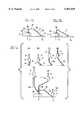
- the loop shape of the wire 3in this case may be a trapezoidal loop shape as shown in FIG. 4(a) or a triangular loop shape as shown in FIG. 4(b).
- the trapezoidal loop shown in FIG. 4(a)is formed by the process shown in FIG. 5.
- step (a) shown in FIG. 5a capillary 4 is lowered so that a ball (not shown) formed on the tip end of the wire 3 is bonded to a first bonding point A. This is done while a damper (not shown), which is located above the capillary 4 and can hold the wire when closed and feed the wire when opened, is opened. After this, the capillary 4 is raised to point B while delivering the wire 3.
- step (b)the capillary is moved horizontally in the opposite direction from the second bonding point G to point C.
- a reverse operationto move the capillary 4 in the direction opposite from the second bonding point G (for forming a loop in the wire) is referred to as a "reverse operation". Because of this reserve operation, the wire 3 assumes a shape that extends from point A to point C; and as a result, a kink 3a is formed in a portion of the wire 3.
- the wire 3 delivered out of the capillary in the process from point A to point Cforms the neck height portion 31 of the loop shown in FIG. 4(a).
- step (c)the capillary 4 is raised to point D while delivering the wire 3.
- step (d)the capillary 4 is again moved horizontally to point E in the opposite direction from the second bonding point G, i. e., another (or second) reverse operation is performed.
- the wire 3assumes a shape inclined From point C to point E, and a kink 3b is formed in a portion of the wire 3.
- the wire 3 delivered out of the capillary 4 in the process from point C to point Eforms the trapezoidal length portion 32 shown in FIG. 5(a).
- step (e)the capillary 4 is raised to point F while delivering the wire 3.
- the amount of wire 3 delivered out of the capillaryis equal to the inclined portion 33 shown in FIG. 5(a).
- the damper(again, not shown) is closed. Once the damper is closed, the wire 3 is not delivered even if the capillary 4 subsequently is moved.
- the capillary 4next makes a circular-arc motion (or a circular-art motion followed by a straight down motion) so that the capillary 4 is positioned at the second bonding point G, and the wire 3 is bonded to the second bonding point G, thus connecting the first and second bonding points A and G.
- the triangular loop shown in FIG. 4(b)is formed by the process shown in FIG. 6.
- the trapezoidal length portion 32 described in the above trapezoidal loop formationis not formed. Accordingly, the second reverse operation in step (d) in FIG. 5 is not performed.
- the steps (c), (d) and (e) in FIG. 6are replaced by the single process as shown in step (c) of FIG. 6.
- the steps (a) and (b)are the same as the steps (a) and (b) shown in FIG. 5, respectively; and after the first reverse operation in step (b) of FIG. 6, the capillary 4 is raised to point F while delivering the wire 3 in step (c).
- the capillary 4performs the operations steps (d) and (e) in the same manner as the operations done in the steps (f) and (g) shown in FIG. 5, so that the wire 3 is bonded to the second bonding point G.
- the triangular loop formation shown in FIG. 6is simpler than the trapezoidal loop formation shown in FIG. 5 and is therefore advantageous in that the loop formation is performed in a shorter time.
- the wire 3tends to come into contact with the edge portion of the semiconductor chip 2 when the triangular wire loop shape as shown in FIG. 4(b) is formed.
- the trapezoidal wire loop formationis employed so as to avoid the contact between the wire 3 and semiconductor chip 2.
- the kinks 3a and 3bare not more easily formed when locations of these kinks are set to be higher from the first bonding point A.
- the kink 3acan be formed relatively easier since the first reverse operation is formed when the capillary 4 is at the position as high as the bonding point A.
- the second reverse operation for forming the second kink 3b in step (d) in FIG. 5is performed with the capillary 4 in a high position which is far away from the first bonding point A.
- the portion of the wire in the vicinity of the kink 3bsee FIG.
- this portion of the wire in the vicinity of the kink 3bmay rise up or drop downward.
- the shape-retaining strength of the portion of the wire near the kink 3bis weak, the wire may bend when pressure from the outside is applied thereon.
- wire bendingmay easily be caused by external forces such as shocks or vibration of the wire 3 due to capillary contact or ultrasonic oscillation during bonding to the second bonding point G, or mold flow due to the injection of molding material during molding, etc.
- the object of the present inventionis to provide a wire bonding method which solves the problems with trapezoidal loops and makes it possible to form a stable wire loop shape which has a high shape-retaining strength.
- the object of the present inventionis accomplished by a unique method in which a first bonding point and a second bonding point are connected by a wire, and the method is characterized in that it comprises: a process in which the wire is connected to the first bonding point; a process of a first reverse operation in which the capillary is raised slightly and then caused to move slightly in the opposite direction from the second bonding point is performed; a process of a second reverse operation in which the capillary is raised and then caused to move in the opposite direction from the second bonding point is performed; a process is performed in which the capillary is raised and then caused to move toward the second bonding point; and a process is performed in which the capillary is raised delivering the wire, the capillary is moved toward the second bonding point, and then the wire is connected to the second bonding point.
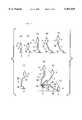
- FIG. 1a-1iis an explanatory diagram which illustrates steps of a wire bonding method according to one embodiment of the present invention
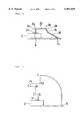
- FIG. 2is a diagram which illustrates the connected the wire
- FIG. 3is a diagram which illustrates the path of the capillary
- FIG. 4(a)shows the trapezoidal wire loop and FIG. 4(b) shows the triangular wire loop of the prior art
- FIG. 5a-5gshows the steps of the prior art to form the trapezoidal wire loop
- FIG. 6a-6eshows the steps of the prior art to form the triangular wire loop.
- FIGS. 1 through 3Constituting elements which are the same as or correspond to those in FIG. 4(a) and FIG. 5 will be labeled with the same symbols in the following description.
- the step (e) shown in FIG. 5 for the trapezoidal loopis changed to steps (e) through (g) of FIG. 1, and the remaining steps are the same as those shown in FIG. 5.
- the steps (a) through (d) in FIG. Icorrespond to the steps (a) through (d) in FIG. 5
- the steps (h) and (i) in FIG. 1correspond to the steps (f) and (g) in FIG. 5.
- step (a)the capillary 4 is lowered so that the ball (not shown) formed at the end of the wire 3 that passes through the capillary 4 is bonded to the first bonding point A. This is done while a damper (not shown), which can hold the wire 3 when closed and feed the wire 3 when opened, is opened. After bonding the ball (or wire) to the first bonding point A, the capillary 4 is raised to point B while delivering the wire 3.
- step (b)a reverse operation is performed.
- the capillary 4is moved horizontally to point C in the direction opposite from the second bonding point G.
- a kink 3ais formed in a portion of the wire 3 in the same manner as in a conventional method.
- the wire 3 delivered out of the capillary 4 during the process from point A to point Cforms a neck height portion 31 of the wire loop (see FIG. 2).
- step (c)the capillary 4 is raised to point D while delivering the wire 3.
- step (d)the capillary 4 is moved in the direction opposite from the second bonding point G.
- a second reverse operationis performed so that the capillary 4 is moved horizontally to point E.
- a kink 3bis formed in the wire 3.
- the wire 3 delivered out of the capillary 4 during the process from point C to Dforms the trapezoidal length portion 32 of the wire loop (see FIG. 2).
- step (e)the capillary 4 is raised to point F1 while delivering the wire 3. Then, in step (f), the capillary 4 is moved toward the second bonding point G. After this movement, as shown in step (g), the capillary 4 is raised to point F while delivering the wire 3.
- a kink 3cis formed in the wire 3.
- the length from the kink 3b to the kink 3ccorresponds to the first inclined portion 34 shown in FIG. 2, and the wire 3 delivered in step (g) forms the second inclined portion 35 shown in FIG. 2.
- the damper(not shown) is closed. Once the damper is thus closed, the wire 3 is not delivered out of the capillary 4 even if the capillary 4 is subsequently moved.
- the capillary 4is moved horizontally toward the second bonding point G and caused to perform a circular-arc motion (or a circular-arc motion followed by a straightly lowering motion) so that the capillary 4 is positioned at the second bonding point G; and then the wire 3 is bonded to the second bonding point G.
- the operation from point F to the second bonding point Ghas no direct connection with the gist of the present invention. Accordingly, it is possible to perform an operation similar to the operation disclosed in the conventional example or to perform some other type of operation.
- the inclined portion 33 shown in the prior art wire loop in FIG. 4(a)comprises two inclined portions: the first inclined portion 34 and the second inclined portion 35 as shown in FIG. 2.
- a kink 3cis formed in the inclined portion 33 so that the area of the kink 3b is stabilized.
- a stronger king 3bis obtained in a high position which is distant from the first bonding point A.
- a wire loop shapethat has a high shape retaining strength can be formed.
- the capillaryis raised slightly after a second reverse operation in which the capillary is moved in the opposite direction from the second bonding point; afterward, the capillary is moved to a position which is more or less above the first bonding point; and then the capillary is raised while delivering the wire. Accordingly, a kink is formed in the inclined portion of the trapezoidal loop. As a result, a stable loop shape can be obtained not only in the case of short loops with a short wiring distance but also in the case of long loops with a long wiring distance. Furthermore, a loop which has a high shape retention strength against pressure applied from the outside can be obtained. Thus, bending of the wire by external pressure can be prevented.
- the obtained loop shapehas a high shock absorption capability with respect to external forces such as shocks to the wire or vibration of the wire due to contact with the capillary, ultrasonic vibration during bonding to the second bonding point, or the flow of molding material caused by injection during molding, etc. Accordingly, bending of the wire can be prevented. Furthermore, a rising loop shape, which tends to be generated in loops on semiconductor devices which contain slight height difference between the first and second bonding points, can be suppressed by the kink formed in the inclined portion of the loop.
Landscapes
- Engineering & Computer Science (AREA)
- Computer Hardware Design (AREA)
- Microelectronics & Electronic Packaging (AREA)
- Power Engineering (AREA)
- Mechanical Engineering (AREA)
- Physics & Mathematics (AREA)
- Condensed Matter Physics & Semiconductors (AREA)
- General Physics & Mathematics (AREA)
- Manufacturing & Machinery (AREA)
- Wire Bonding (AREA)
Abstract
Description
Claims (2)
Applications Claiming Priority (2)
| Application Number | Priority Date | Filing Date | Title |
|---|---|---|---|
| JP01479897AJP3370539B2 (en) | 1997-01-13 | 1997-01-13 | Wire bonding method |
| JP9-014798 | 1997-01-13 |
Publications (1)
| Publication Number | Publication Date |
|---|---|
| US5961029Atrue US5961029A (en) | 1999-10-05 |
Family
ID=11871078
Family Applications (1)
| Application Number | Title | Priority Date | Filing Date |
|---|---|---|---|
| US09/005,789Expired - LifetimeUS5961029A (en) | 1997-01-13 | 1998-01-12 | Wire bonding method |
Country Status (4)
| Country | Link |
|---|---|
| US (1) | US5961029A (en) |
| JP (1) | JP3370539B2 (en) |
| KR (1) | KR100274820B1 (en) |
| TW (1) | TW388091B (en) |
Cited By (18)
| Publication number | Priority date | Publication date | Assignee | Title |
|---|---|---|---|---|
| US6161753A (en)* | 1999-11-01 | 2000-12-19 | Advanced Semiconductor Engineering, Inc. | Method of making a low-profile wire connection for stacked dies |
| US6176416B1 (en)* | 1999-07-02 | 2001-01-23 | Advanced Semiconductor Engineering, Inc. | Method of making low-profile wire connection |
| US6213384B1 (en)* | 1997-10-27 | 2001-04-10 | Kabushiki Kaisha Shinkawa | Wire bonding method |
| US6315190B1 (en)* | 1998-06-25 | 2001-11-13 | Kabushiki Kaisha Shinkawa | Wire bonding method |
| US6380634B1 (en)* | 1998-07-27 | 2002-04-30 | Texas Instruments Incorporated | Conductor wires and semiconductor device using them |
| US6391759B1 (en)* | 2000-04-27 | 2002-05-21 | Advanced Semiconductor Engineering, Inc. | Bonding method which prevents wire sweep and the wire structure thereof |
| US6457235B1 (en)* | 2000-06-09 | 2002-10-01 | Advanced Semiconductor Engineering, Inc. | Method of wire-bonding circuit chip to bonding pad |
| EP1422014A1 (en)* | 2002-11-21 | 2004-05-26 | Kaijo Corporation | Semiconductor device having a wire loop with a crushed part on a ball, loop wire bonding method and loop wire bonding apparatus for carrying out such method |
| US20050072833A1 (en)* | 2003-10-02 | 2005-04-07 | Wong Yam Mo | Method of forming low wire loops and wire loops formed using the method |
| US20050109819A1 (en)* | 2003-11-26 | 2005-05-26 | Kulicke & Soffa Industries, Inc. | Low loop height ball bonding method and apparatus |
| US20060032894A1 (en)* | 2004-08-13 | 2006-02-16 | Asm Technology Singapore Pte Ltd | Wire bond with improved shear strength |
| US20060151579A1 (en)* | 2005-01-11 | 2006-07-13 | Hiromi Fujisawa | Wire loop, semiconductor device having same and wire bonding method |
| US20060255101A1 (en)* | 2005-05-10 | 2006-11-16 | Mizuho Shirato | Wire loop, semiconductor device having same and wire bonding method |
| US20070015353A1 (en)* | 2005-07-14 | 2007-01-18 | Craig David M | Electrically connecting substrate with electrical device |
| US20070284416A1 (en)* | 2006-06-02 | 2007-12-13 | Yam Mo Wong | Wire bonding method for forming low-loop profiles |
| US20100147552A1 (en)* | 2007-04-02 | 2010-06-17 | Kulicke And Soffa Industries, Inc. | Method of forming bends in a wire loop |
| CN108074900A (en)* | 2016-11-15 | 2018-05-25 | 先进科技新加坡有限公司 | The conductor loop for forming the method for three-dimensional wire ring and being formed using this method |
| US10600756B1 (en) | 2017-02-15 | 2020-03-24 | United States Of America, As Represented By The Secretary Of The Navy | Wire bonding technique for integrated circuit board connections |
Citations (12)
| Publication number | Priority date | Publication date | Assignee | Title |
|---|---|---|---|---|
| US4327860A (en)* | 1980-01-03 | 1982-05-04 | Kulicke And Soffa Ind. Inc. | Method of making slack free wire interconnections |
| US4597522A (en)* | 1983-12-26 | 1986-07-01 | Kabushiki Kaisha Toshiba | Wire bonding method and device |
| US4932584A (en)* | 1986-08-08 | 1990-06-12 | Kabushiki Kaisha Shinkawa | Method of wire bonding |
| US5148964A (en)* | 1990-02-13 | 1992-09-22 | Kabushiki Kaisha Toshiba | Wire bonding method |
| US5156323A (en)* | 1991-02-27 | 1992-10-20 | Kabushiki Kaisha Shinkawa | Wire bonding method |
| US5158223A (en)* | 1990-06-08 | 1992-10-27 | Kabushiki Kaisha Toshiba | Wire bonding apparatus |
| JPH04318943A (en)* | 1991-04-17 | 1992-11-10 | Toshiba Corp | wire bonding equipment |
| US5192018A (en)* | 1991-02-27 | 1993-03-09 | Kabushiki Kaisha Shinkawa | Wire bonding method |
| JPH0560657A (en)* | 1991-09-02 | 1993-03-12 | Nippon Seiko Kk | Device for measuring pitch of outer ring raceway of double row ball bearing |
| US5205463A (en)* | 1992-06-05 | 1993-04-27 | Kulicke And Soffa Investments, Inc. | Method of making constant clearance flat link fine wire interconnections |
| US5259548A (en)* | 1991-06-19 | 1993-11-09 | Kabushiki Kaisha Shinkawa | Wire bonding method |
| US5452841A (en)* | 1993-07-23 | 1995-09-26 | Nippondenso Co., Ltd. | Wire bonding apparatus and method |
- 1997
- 1997-01-13JPJP01479897Apatent/JP3370539B2/ennot_activeExpired - Fee Related
- 1997-11-25TWTW086117647Apatent/TW388091B/enactive
- 1997-12-11KRKR1019970067918Apatent/KR100274820B1/ennot_activeExpired - Fee Related
- 1998
- 1998-01-12USUS09/005,789patent/US5961029A/ennot_activeExpired - Lifetime
Patent Citations (12)
| Publication number | Priority date | Publication date | Assignee | Title |
|---|---|---|---|---|
| US4327860A (en)* | 1980-01-03 | 1982-05-04 | Kulicke And Soffa Ind. Inc. | Method of making slack free wire interconnections |
| US4597522A (en)* | 1983-12-26 | 1986-07-01 | Kabushiki Kaisha Toshiba | Wire bonding method and device |
| US4932584A (en)* | 1986-08-08 | 1990-06-12 | Kabushiki Kaisha Shinkawa | Method of wire bonding |
| US5148964A (en)* | 1990-02-13 | 1992-09-22 | Kabushiki Kaisha Toshiba | Wire bonding method |
| US5158223A (en)* | 1990-06-08 | 1992-10-27 | Kabushiki Kaisha Toshiba | Wire bonding apparatus |
| US5156323A (en)* | 1991-02-27 | 1992-10-20 | Kabushiki Kaisha Shinkawa | Wire bonding method |
| US5192018A (en)* | 1991-02-27 | 1993-03-09 | Kabushiki Kaisha Shinkawa | Wire bonding method |
| JPH04318943A (en)* | 1991-04-17 | 1992-11-10 | Toshiba Corp | wire bonding equipment |
| US5259548A (en)* | 1991-06-19 | 1993-11-09 | Kabushiki Kaisha Shinkawa | Wire bonding method |
| JPH0560657A (en)* | 1991-09-02 | 1993-03-12 | Nippon Seiko Kk | Device for measuring pitch of outer ring raceway of double row ball bearing |
| US5205463A (en)* | 1992-06-05 | 1993-04-27 | Kulicke And Soffa Investments, Inc. | Method of making constant clearance flat link fine wire interconnections |
| US5452841A (en)* | 1993-07-23 | 1995-09-26 | Nippondenso Co., Ltd. | Wire bonding apparatus and method |
Cited By (36)
| Publication number | Priority date | Publication date | Assignee | Title |
|---|---|---|---|---|
| US6213384B1 (en)* | 1997-10-27 | 2001-04-10 | Kabushiki Kaisha Shinkawa | Wire bonding method |
| US6315190B1 (en)* | 1998-06-25 | 2001-11-13 | Kabushiki Kaisha Shinkawa | Wire bonding method |
| US6380634B1 (en)* | 1998-07-27 | 2002-04-30 | Texas Instruments Incorporated | Conductor wires and semiconductor device using them |
| US6176416B1 (en)* | 1999-07-02 | 2001-01-23 | Advanced Semiconductor Engineering, Inc. | Method of making low-profile wire connection |
| US6161753A (en)* | 1999-11-01 | 2000-12-19 | Advanced Semiconductor Engineering, Inc. | Method of making a low-profile wire connection for stacked dies |
| US6391759B1 (en)* | 2000-04-27 | 2002-05-21 | Advanced Semiconductor Engineering, Inc. | Bonding method which prevents wire sweep and the wire structure thereof |
| US6457235B1 (en)* | 2000-06-09 | 2002-10-01 | Advanced Semiconductor Engineering, Inc. | Method of wire-bonding circuit chip to bonding pad |
| US20040104477A1 (en)* | 2002-11-21 | 2004-06-03 | Hiromi Fujisawa | Wire loop, semiconductor device having same, wire bonding method and wire bonding apparatus |
| EP1422014A1 (en)* | 2002-11-21 | 2004-05-26 | Kaijo Corporation | Semiconductor device having a wire loop with a crushed part on a ball, loop wire bonding method and loop wire bonding apparatus for carrying out such method |
| US6933608B2 (en) | 2002-11-21 | 2005-08-23 | Kaijo Corporation | Wire loop, semiconductor device having same, wire bonding method and wire bonding apparatus |
| US20050189567A1 (en)* | 2002-11-21 | 2005-09-01 | Hiromi Fujisawa | Wire loop, semiconductor device having same, wire bonding method and wire bonding apparatus |
| CN100409422C (en)* | 2002-11-21 | 2008-08-06 | 株式会社海上 | Wire ring and semiconductor device thereof, wire bonding method and wire bonding device |
| US20050072833A1 (en)* | 2003-10-02 | 2005-04-07 | Wong Yam Mo | Method of forming low wire loops and wire loops formed using the method |
| US7494042B2 (en) | 2003-10-02 | 2009-02-24 | Asm Technology Singapore Pte. Ltd. | Method of forming low wire loops and wire loops formed using the method |
| US20050109819A1 (en)* | 2003-11-26 | 2005-05-26 | Kulicke & Soffa Industries, Inc. | Low loop height ball bonding method and apparatus |
| US7584881B2 (en) | 2003-11-26 | 2009-09-08 | Kulicke And Soffa Industries, Inc. | Low loop height ball bonding method and apparatus |
| US20080111252A1 (en)* | 2003-11-26 | 2008-05-15 | Kulicke And Soffa Industries, Inc. | Low loop height ball bonding method and apparatus |
| US7347352B2 (en)* | 2003-11-26 | 2008-03-25 | Kulicke And Soffa Industries, Inc. | Low loop height ball bonding method and apparatus |
| US7314157B2 (en)* | 2004-08-13 | 2008-01-01 | Asm Technology Singapore Pte Ltd | Wire bond with improved shear strength |
| US20060032894A1 (en)* | 2004-08-13 | 2006-02-16 | Asm Technology Singapore Pte Ltd | Wire bond with improved shear strength |
| US20060151579A1 (en)* | 2005-01-11 | 2006-07-13 | Hiromi Fujisawa | Wire loop, semiconductor device having same and wire bonding method |
| US7815095B2 (en) | 2005-01-11 | 2010-10-19 | Kaijo Corporation | Wire loop, semiconductor device having same and wire bonding method |
| US20060255101A1 (en)* | 2005-05-10 | 2006-11-16 | Mizuho Shirato | Wire loop, semiconductor device having same and wire bonding method |
| US8016182B2 (en) | 2005-05-10 | 2011-09-13 | Kaijo Corporation | Wire loop, semiconductor device having same and wire bonding method |
| TWI416672B (en)* | 2005-07-14 | 2013-11-21 | Hewlett Packard Development Co | Electrically connecting substrate with electrical device |
| US20070015353A1 (en)* | 2005-07-14 | 2007-01-18 | Craig David M | Electrically connecting substrate with electrical device |
| US7476608B2 (en)* | 2005-07-14 | 2009-01-13 | Hewlett-Packard Development Company, L.P. | Electrically connecting substrate with electrical device |
| US20090014850A1 (en)* | 2005-07-14 | 2009-01-15 | Craig David M | Electrically Connecting Substrate With Electrical Device |
| US7576439B2 (en) | 2005-07-14 | 2009-08-18 | Hewlett-Packard Development Company, L.P. | Electrically connecting substrate with electrical device |
| US20070284416A1 (en)* | 2006-06-02 | 2007-12-13 | Yam Mo Wong | Wire bonding method for forming low-loop profiles |
| US7780064B2 (en)* | 2006-06-02 | 2010-08-24 | Asm Technology Singapore Pte Ltd | Wire bonding method for forming low-loop profiles |
| US20100147552A1 (en)* | 2007-04-02 | 2010-06-17 | Kulicke And Soffa Industries, Inc. | Method of forming bends in a wire loop |
| US8063305B2 (en)* | 2007-04-02 | 2011-11-22 | Kulicke And Soffa Industries, Inc. | Method of forming bends in a wire loop |
| CN108074900A (en)* | 2016-11-15 | 2018-05-25 | 先进科技新加坡有限公司 | The conductor loop for forming the method for three-dimensional wire ring and being formed using this method |
| CN108074900B (en)* | 2016-11-15 | 2021-01-15 | 先进科技新加坡有限公司 | Method of forming three-dimensional wire loop and wire loop formed using the same |
| US10600756B1 (en) | 2017-02-15 | 2020-03-24 | United States Of America, As Represented By The Secretary Of The Navy | Wire bonding technique for integrated circuit board connections |
Also Published As
| Publication number | Publication date |
|---|---|
| TW388091B (en) | 2000-04-21 |
| JP3370539B2 (en) | 2003-01-27 |
| KR100274820B1 (en) | 2001-01-15 |
| KR19980070152A (en) | 1998-10-26 |
| JPH10199916A (en) | 1998-07-31 |
Similar Documents
| Publication | Publication Date | Title |
|---|---|---|
| US5989995A (en) | Semiconductor device and wire bonding method therefor | |
| US5961029A (en) | Wire bonding method | |
| US6933608B2 (en) | Wire loop, semiconductor device having same, wire bonding method and wire bonding apparatus | |
| US7815095B2 (en) | Wire loop, semiconductor device having same and wire bonding method | |
| US5967401A (en) | Wire bonding method | |
| US6112974A (en) | Wire bonding method | |
| US6222274B1 (en) | Bonding wire loop shape for a semiconductor device | |
| US6343733B1 (en) | Wire bonding method | |
| US6315190B1 (en) | Wire bonding method | |
| US6036080A (en) | Wire bonding method | |
| US6182885B1 (en) | Wire bonding method | |
| US6250539B1 (en) | Wire bonding method | |
| JPH10125708A (en) | Semiconductor device |
Legal Events
| Date | Code | Title | Description |
|---|---|---|---|
| AS | Assignment | Owner name:KABUSHIKI KAISHA SHINKAWA, JAPAN Free format text:ASSIGNMENT OF ASSIGNORS INTEREST;ASSIGNORS:NISHIURA, SHINICHI;MOCHIDA, TOORU;REEL/FRAME:008962/0477 Effective date:19980105 | |
| STCF | Information on status: patent grant | Free format text:PATENTED CASE | |
| FEPP | Fee payment procedure | Free format text:PAYOR NUMBER ASSIGNED (ORIGINAL EVENT CODE: ASPN); ENTITY STATUS OF PATENT OWNER: LARGE ENTITY | |
| FPAY | Fee payment | Year of fee payment:4 | |
| FPAY | Fee payment | Year of fee payment:8 | |
| FEPP | Fee payment procedure | Free format text:PAYER NUMBER DE-ASSIGNED (ORIGINAL EVENT CODE: RMPN); ENTITY STATUS OF PATENT OWNER: LARGE ENTITY Free format text:PAYOR NUMBER ASSIGNED (ORIGINAL EVENT CODE: ASPN); ENTITY STATUS OF PATENT OWNER: LARGE ENTITY | |
| FPAY | Fee payment | Year of fee payment:12 | |
| FEPP | Fee payment procedure | Free format text:PAT HOLDER NO LONGER CLAIMS SMALL ENTITY STATUS, ENTITY STATUS SET TO UNDISCOUNTED (ORIGINAL EVENT CODE: STOL); ENTITY STATUS OF PATENT OWNER: LARGE ENTITY |