US5960322A - Suppression of boron segregation for shallow source and drain junctions in semiconductors - Google Patents
Suppression of boron segregation for shallow source and drain junctions in semiconductorsDownload PDFInfo
- Publication number
- US5960322A US5960322AUS08/994,308US99430897AUS5960322AUS 5960322 AUS5960322 AUS 5960322AUS 99430897 AUS99430897 AUS 99430897AUS 5960322 AUS5960322 AUS 5960322A
- Authority
- US
- United States
- Prior art keywords
- screen
- gate
- layer
- dopant
- oxide layer
- Prior art date
- Legal status (The legal status is an assumption and is not a legal conclusion. Google has not performed a legal analysis and makes no representation as to the accuracy of the status listed.)
- Expired - Lifetime
Links
Images


Classifications
- H—ELECTRICITY
- H01—ELECTRIC ELEMENTS
- H01L—SEMICONDUCTOR DEVICES NOT COVERED BY CLASS H10
- H01L21/00—Processes or apparatus adapted for the manufacture or treatment of semiconductor or solid state devices or of parts thereof
- H01L21/02—Manufacture or treatment of semiconductor devices or of parts thereof
- H01L21/04—Manufacture or treatment of semiconductor devices or of parts thereof the devices having potential barriers, e.g. a PN junction, depletion layer or carrier concentration layer
- H01L21/18—Manufacture or treatment of semiconductor devices or of parts thereof the devices having potential barriers, e.g. a PN junction, depletion layer or carrier concentration layer the devices having semiconductor bodies comprising elements of Group IV of the Periodic Table or AIIIBV compounds with or without impurities, e.g. doping materials
- H01L21/26—Bombardment with radiation
- H01L21/263—Bombardment with radiation with high-energy radiation
- H01L21/265—Bombardment with radiation with high-energy radiation producing ion implantation
- H01L21/26506—Bombardment with radiation with high-energy radiation producing ion implantation in group IV semiconductors
- H01L21/26513—Bombardment with radiation with high-energy radiation producing ion implantation in group IV semiconductors of electrically active species
- H01L21/2652—Through-implantation
- H—ELECTRICITY
- H01—ELECTRIC ELEMENTS
- H01L—SEMICONDUCTOR DEVICES NOT COVERED BY CLASS H10
- H01L21/00—Processes or apparatus adapted for the manufacture or treatment of semiconductor or solid state devices or of parts thereof
- H01L21/02—Manufacture or treatment of semiconductor devices or of parts thereof
- H01L21/04—Manufacture or treatment of semiconductor devices or of parts thereof the devices having potential barriers, e.g. a PN junction, depletion layer or carrier concentration layer
- H01L21/18—Manufacture or treatment of semiconductor devices or of parts thereof the devices having potential barriers, e.g. a PN junction, depletion layer or carrier concentration layer the devices having semiconductor bodies comprising elements of Group IV of the Periodic Table or AIIIBV compounds with or without impurities, e.g. doping materials
- H01L21/26—Bombardment with radiation
- H01L21/263—Bombardment with radiation with high-energy radiation
- H01L21/265—Bombardment with radiation with high-energy radiation producing ion implantation
- H01L21/2658—Bombardment with radiation with high-energy radiation producing ion implantation of a molecular ion, e.g. decaborane
- H—ELECTRICITY
- H10—SEMICONDUCTOR DEVICES; ELECTRIC SOLID-STATE DEVICES NOT OTHERWISE PROVIDED FOR
- H10D—INORGANIC ELECTRIC SEMICONDUCTOR DEVICES
- H10D30/00—Field-effect transistors [FET]
- H10D30/01—Manufacture or treatment
- H10D30/021—Manufacture or treatment of FETs having insulated gates [IGFET]
- H10D30/0223—Manufacture or treatment of FETs having insulated gates [IGFET] having source and drain regions or source and drain extensions self-aligned to sides of the gate
- H10D30/0227—Manufacture or treatment of FETs having insulated gates [IGFET] having source and drain regions or source and drain extensions self-aligned to sides of the gate having both lightly-doped source and drain extensions and source and drain regions self-aligned to the sides of the gate, e.g. lightly-doped drain [LDD] MOSFET or double-diffused drain [DDD] MOSFET
- H—ELECTRICITY
- H10—SEMICONDUCTOR DEVICES; ELECTRIC SOLID-STATE DEVICES NOT OTHERWISE PROVIDED FOR
- H10D—INORGANIC ELECTRIC SEMICONDUCTOR DEVICES
- H10D64/00—Electrodes of devices having potential barriers
- H10D64/01—Manufacture or treatment
- H10D64/021—Manufacture or treatment using multiple gate spacer layers, e.g. bilayered sidewall spacers
- Y—GENERAL TAGGING OF NEW TECHNOLOGICAL DEVELOPMENTS; GENERAL TAGGING OF CROSS-SECTIONAL TECHNOLOGIES SPANNING OVER SEVERAL SECTIONS OF THE IPC; TECHNICAL SUBJECTS COVERED BY FORMER USPC CROSS-REFERENCE ART COLLECTIONS [XRACs] AND DIGESTS
- Y10—TECHNICAL SUBJECTS COVERED BY FORMER USPC
- Y10S—TECHNICAL SUBJECTS COVERED BY FORMER USPC CROSS-REFERENCE ART COLLECTIONS [XRACs] AND DIGESTS
- Y10S438/00—Semiconductor device manufacturing: process
- Y10S438/914—Doping
- Y10S438/917—Deep level dopants, e.g. gold, chromium, iron or nickel
Definitions
- the present inventionrelates generally to semiconductor manufacturing technology and more specifically to deep-submicron P-channel Metal-Oxide Semiconductor (MOS) transistor manufacturing.
- MOSMetal-Oxide Semiconductor
- CMOSDeep-submicron Complementary Metal-Oxide-Semiconductor
- ULSIultra-large scale integrated circuits.
- SCEshort channel effects
- a major problem related to source and drain junctionsis that the source and drain series resistance increases as the devices are scaled down, which degrade the device performance.
- shallow source and drain junctionsconsist of shallow source and drain extension junctions to suppress SCE, and relatively deep source and drain junctions to improve series resistance.
- the resistance from shallow source and drain extension junctionsis a large portion of the total series resistance. As extension junctions become shallower and shallower, the series resistance tends to become greater and greater. In order to make the source and drain series resistance low, high doping density is needed in the shallow extension junctions.
- the shallow source and drain extension junctions and the relatively deep source and drain junctionsare implemented by ion implantation of dopant through a screen oxide (Si0 2 ) layer.
- Implantation through an oxide layerresults in the deposition of recoiled oxygen into the silicon.
- This oxygenhas a tendency to reduce the interstitial silicon which is present in the implant-damaged substrate. This, in turn, suppresses the diffusion tail associated with the implanted dopant, which moves by an interstitialcy mechanism. This increases the series resistance.
- NMOSN-channel Metal-Oxide-Semiconductor
- Group V elementsare used as dopants.
- boron (B)is the most commonly used dopant for both the shallow extension junctions and the relatively deep source and drain junctions. Boron is incorporated into the silicon through ion implantation of either boron atoms or boron difluoride (BF 2 ).
- the dopantsneed to be activated by a thermal treatment-usually a rapid thermal annealing (RTA).
- RTArapid thermal annealing
- boron atomstend to segregate from the silicon substrate into the screen oxide layer during the RTA of dopant activation.
- Boron segregationresults in a decrease of boron concentration in the silicon substrate near its surface and therefore an increase of source and drain series resistance. This effect becomes more and more of a problem as device sizes are continuously scaled down and the extension and junction depths becomes shallower and shallower.
- the present inventionovercomes the problem that dopant atoms tend to segregate from silicon substrate into the screen oxide layer during the RTA of dopant activation by nitridizing the screen oxide layer into the oxynitride before the implantation of the dopant.
- the present inventionhas the advantage of suppressing boron loss in silicon through segregation into the screen oxide layer during the boron activation RTA.
- the present inventionalso has the advantage of providing advanced, deep submicron CMOS devices with overall ultra-shallow junctions which have low series resistance.
- FIG. 1is a cross-section of a semiconductor transistor gate area
- FIG. 2is the semiconductor of FIG. 1 after screen oxide layer deposition
- FIG. 3is the semiconductor of FIG. 2 after screen oxide layer nitridation
- FIG. 4is the semiconductor of FIG. 3 during shallow source and drain extension junction implantation
- FIG. 5is the semiconductor of FIG. 4 after conformal oxide layer deposition
- FIG. 6is the semiconductor of FIG. 5 after spacer etching
- FIG. 7is the semiconductor of FIG. 6 after screen oxide layer deposition
- FIG. 8is the semiconductor of FIG. 7 after screen oxide layer nitridation
- FIG. 9is the semiconductor of FIG. 8 during deep source and drain junction implantation
- FIG. 10is the semiconductor of FIG. 9 after rapid thermal annealing.
- FIG. 11is the semiconductor of FIG. 10 after removal of the screen oxynitride layer.
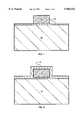
- FIG. 1therein is shown a cross-section of a partially processed semiconductor wafer.
- the semiconductor waferhas been processed to the point at which a silicon substrate 10 has a silicon dioxide (SiO 2 ) gate oxide layer 12 deposited on top.
- a silicon dioxide (SiO 2 ) gate oxide layer 12deposited on top.
- a polysilicon (polycrystalline silicon) gate 14is positioned over an area or well of N - silicon.
- FIG. 2therein is shown the silicon substrate 10 and the polysilicon gate 14 having a screen oxide layer 16 of silicon dioxide deposited thereon.
- FIG. 3therein is shown a screen oxynitride layer 18 after nitridation which converts the silicon dioxide of the screen oxide layer 16 of FIG. 2 into a silicon oxynitride.
- FIG. 4therein is shown the boron implantation 19 of the silicon substrate 10 to form the initial ultra-shallow, P-silicon source and drain junctions in the well of N - silicon. These initial junctions are designated as source and drain extension junctions 20 and 22. They are formed by ion implantation through the screen oxynitride layer 18.
- FIG. 5therein is shown a conformal oxide layer 24 deposited on the screen oxynitride layer 18.
- FIG. 6therein is shown the conformal oxide layer 24 and the screen oxynitride layer 18 after etching to form sidewall spacers and to expose the polysilicon gate 14 and the source and drain extension junctions 20 and 22.
- FIG. 7therein is shown another, second screen oxide layer 26 deposited over the semiconductor wafer to cover the polysilicon gate 14 and the source and drain extension junctions 20 and 22.
- FIG. 8therein is shown a second screen oxynitride layer 28 after nitridation which converts the silicon dioxide of the screen oxide layer 26 of FIG. 7 into silicon oxynitride.
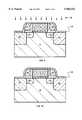
- FIG. 9therein is shown another, second boron implantation 29 of the silicon substrate 10 to form the relatively deep P-silicon source and drain junctions in the well of N - silicon. These junctions are designated as source and drain junctions 30 and 32, respectively, and are integral with the source and drain extension junctions 20 and 22.
- the source and drain junctions 30 and 32are formed by ion implantation through the screen oxynitride layer 28.
- FIG. 10therein is shown the deep-submicron CMOS transistor after the rapid thermal annealing for boron activation.
- FIG. 11therein is shown the second screen oxynitride layer 28 etched away and the transistor ready for the remaining conventional processing.
- the remaining conventional processingwould be evident to those skilled in the art as required to produce finished deep submicron (sub-0.1 micron) ultra large scale integrated (ULSI) circuit devices.
- the process flow for the present inventionstarts with the silicon substrate 10 having been processed with wells of N - silicon and the deposition of the silicon dioxide gate oxide layer 12 and the polysilicon gate 14.
- the screen oxide layer 16 of silicon dioxideis then deposited as shown in FIG. 2, generally by low pressure chemical vapor deposition (LPCVD).
- LPCVDlow pressure chemical vapor deposition
- a nitridation of the screen oxide layer 16is performed.
- the nitridationis a rapid thermal annealing process in a gaseous nitrogen compound ambient.
- the rapid thermal annealing temperaturewould be around 900° C. for 30 seconds.
- the gaseous nitrogen compoundsinclude ammonia (NH 3 ), nitric oxide (NO), and nitrous oxide (N 2 O).
- Furnace annealingcan also be used, but rapid thermal annealing is preferred for less doping redistribution.
- ammonia and nitric oxide rapid thermal annealingin particular are preferred, because they can incorporate more nitrogen into the screen oxide layer 16 with a peak near the interface with the silicon substrate 10.
- the pure oxide of the screen oxide layer 16will be turned into an oxynitride to form the screen oxynitride layer 18, as shown in FIG. 3.
- the fundamental principleis that nitrogen in oxides can significantly suppress boron diffusion and segregation into the oxides.
- a dopantis implanted through the screen oxynitride layer 18 into the silicon substrate 10 to form the ultra-shallow, P-silicon source and drain extension junctions 20 and 22, as shown in FIG. 4.
- the conduction-increasing boron (B) dopant for P-silicon formationis ion implanted as elemental boron or as boron difluoride (BF 2 ).
- the conformal oxide layer 24is deposited over the screen oxynitride layer 18, as shown in FIG. 5.
- the conformal oxide layer 24 and the screen oxynitride layer 18are then subject to an anisotropic reactive ion etch (RIE) process to arrive at the configuration shown in FIG. 6.
- RIEreactive ion etch
- the anisotropic etchuses the silicon of the silicon substrate 10 and of the polysilicon gate 14 as etch stops, and the etching continues until the silicon is exposed. This leaves the conformal oxide layer 24 as oxide spacers 24 against the oxynitride on the sides of and around the polysilicon gate 14.
- Another second screen oxide layer 26is then deposited again by LPCVD over the wafer, as shown in FIG. 7, and another nitridation is performed.
- the conditions of this second nitridationwould be the same as previously described for the first nitridation step. Again, this turns the pure oxide in the screen oxide layer 26 of FIG. 7 into oxynitride to form the second screen oxynitride layer 28, as shown in FIG. 8.
- boron (B) or boron difluoride (BF 2 )is ion implanted through the screen oxynitride layer 28 into the silicon substrate 10 as shown in FIG. 9. This time, the implantation of the source and drain junctions 30 and 32 proceeds to create relatively deep junctions as compared to the ultra-shallow extension junctions 20 and 22.
- the oxide layer 24absorbs the boron near the polysilicon gate 14 and prevents the shallow extension junctions 20 and 22 from getting significantly deeper.
- a final rapid thermal anneal of the present inventionis performed in a gaseous nitrogen (N 2 ) atmosphere for activation of the boron in the silicon substrate 10, as shown in FIG. 10.
- Typical conditionsare a temperature of about 1050° C. and a time of about 30 seconds. Because of the screen oxynitride layer 28 on the surface of silicon substrate 10 in the boron implanted region, the segregation of boron from these implanted regions will be significantly suppressed or even totally stopped. This boron retention will improve the conductivity of the implanted region consisting of the source and drain extension junctions and junctions 20, 22, 30, and 32. This reduces the series resistance and increases the drive current of ULSI circuit devices.
- a removal of the screen oxynitride layer 28is carried out after the above final rapid thermal anneal by conventional wet etching to arrive at the configuration shown in FIG. 11. After this step, process flow of the ULSI device fabrication is conventional.
Landscapes
- Physics & Mathematics (AREA)
- Engineering & Computer Science (AREA)
- High Energy & Nuclear Physics (AREA)
- General Physics & Mathematics (AREA)
- Toxicology (AREA)
- Condensed Matter Physics & Semiconductors (AREA)
- Health & Medical Sciences (AREA)
- Manufacturing & Machinery (AREA)
- Computer Hardware Design (AREA)
- Microelectronics & Electronic Packaging (AREA)
- Power Engineering (AREA)
- Spectroscopy & Molecular Physics (AREA)
- Insulated Gate Type Field-Effect Transistor (AREA)
Abstract
Description
Claims (11)
Priority Applications (1)
| Application Number | Priority Date | Filing Date | Title |
|---|---|---|---|
| US08/994,308US5960322A (en) | 1997-12-19 | 1997-12-19 | Suppression of boron segregation for shallow source and drain junctions in semiconductors |
Applications Claiming Priority (1)
| Application Number | Priority Date | Filing Date | Title |
|---|---|---|---|
| US08/994,308US5960322A (en) | 1997-12-19 | 1997-12-19 | Suppression of boron segregation for shallow source and drain junctions in semiconductors |
Publications (1)
| Publication Number | Publication Date |
|---|---|
| US5960322Atrue US5960322A (en) | 1999-09-28 |
Family
ID=25540528
Family Applications (1)
| Application Number | Title | Priority Date | Filing Date |
|---|---|---|---|
| US08/994,308Expired - LifetimeUS5960322A (en) | 1997-12-19 | 1997-12-19 | Suppression of boron segregation for shallow source and drain junctions in semiconductors |
Country Status (1)
| Country | Link |
|---|---|
| US (1) | US5960322A (en) |
Cited By (43)
| Publication number | Priority date | Publication date | Assignee | Title |
|---|---|---|---|---|
| US6214682B1 (en)* | 1999-05-27 | 2001-04-10 | Taiwan Semiconductor Manufacturing Company | Method for fabricating an ultra-shallow junction with low resistance using a rapid thermal anneal in ammonia to increase activation ratio and reduce diffusion of lightly doped source and drain regions |
| US20030134517A1 (en)* | 2000-01-20 | 2003-07-17 | Matsushita Electric Industrial Co., Ltd. | Semiconductor device and method for fabricating the same |
| US6660635B1 (en) | 2002-03-20 | 2003-12-09 | Taiwan Semiconductor Manufacturing Company | Pre-LDD wet clean recipe to gain channel length scaling margin beyond sub-0.1 μm |
| KR100425989B1 (en)* | 2002-08-22 | 2004-04-06 | 동부전자 주식회사 | Method For Manufacturing Semiconductor Devices |
| US6797559B2 (en)* | 2002-04-04 | 2004-09-28 | Samsung Electronics Co., Ltd. | Method of fabricating semiconductor device having metal conducting layer |
| US20040206950A1 (en)* | 2003-04-18 | 2004-10-21 | Agajan Suvkhanov | Ion recoil implantation and enhanced carrier mobility in CMOS device |
| US20040206951A1 (en)* | 2003-04-18 | 2004-10-21 | Mirabedini Mohammad R. | Ion implantation in channel region of CMOS device for enhanced carrier mobility |
| US20090081858A1 (en)* | 2007-09-26 | 2009-03-26 | Shu Qin | Sputtering-Less Ultra-Low Energy Ion Implantation |
| US8324059B2 (en) | 2011-04-25 | 2012-12-04 | United Microelectronics Corp. | Method of fabricating a semiconductor structure |
| US8426284B2 (en) | 2011-05-11 | 2013-04-23 | United Microelectronics Corp. | Manufacturing method for semiconductor structure |
| US8431460B2 (en) | 2011-05-27 | 2013-04-30 | United Microelectronics Corp. | Method for fabricating semiconductor device |
| US8445363B2 (en) | 2011-04-21 | 2013-05-21 | United Microelectronics Corp. | Method of fabricating an epitaxial layer |
| US8466502B2 (en) | 2011-03-24 | 2013-06-18 | United Microelectronics Corp. | Metal-gate CMOS device |
| US8476169B2 (en) | 2011-10-17 | 2013-07-02 | United Microelectronics Corp. | Method of making strained silicon channel semiconductor structure |
| US8481391B2 (en) | 2011-05-18 | 2013-07-09 | United Microelectronics Corp. | Process for manufacturing stress-providing structure and semiconductor device with such stress-providing structure |
| US8575043B2 (en) | 2011-07-26 | 2013-11-05 | United Microelectronics Corp. | Semiconductor device and manufacturing method thereof |
| US20130302964A1 (en)* | 2012-05-09 | 2013-11-14 | Samsung Electronics Co., Ltd. | Semiconductor device and method of fabricating the same |
| US8647953B2 (en) | 2011-11-17 | 2014-02-11 | United Microelectronics Corp. | Method for fabricating first and second epitaxial cap layers |
| US8647941B2 (en) | 2011-08-17 | 2014-02-11 | United Microelectronics Corp. | Method of forming semiconductor device |
| US8664069B2 (en) | 2012-04-05 | 2014-03-04 | United Microelectronics Corp. | Semiconductor structure and process thereof |
| US8674433B2 (en) | 2011-08-24 | 2014-03-18 | United Microelectronics Corp. | Semiconductor process |
| US8691659B2 (en) | 2011-10-26 | 2014-04-08 | United Microelectronics Corp. | Method for forming void-free dielectric layer |
| US8710632B2 (en) | 2012-09-07 | 2014-04-29 | United Microelectronics Corp. | Compound semiconductor epitaxial structure and method for fabricating the same |
| US8709930B2 (en) | 2011-11-25 | 2014-04-29 | United Microelectronics Corp. | Semiconductor process |
| US8716750B2 (en) | 2011-07-25 | 2014-05-06 | United Microelectronics Corp. | Semiconductor device having epitaxial structures |
| US8753902B1 (en) | 2013-03-13 | 2014-06-17 | United Microelectronics Corp. | Method of controlling etching process for forming epitaxial structure |
| US8754448B2 (en) | 2011-11-01 | 2014-06-17 | United Microelectronics Corp. | Semiconductor device having epitaxial layer |
| US8765546B1 (en) | 2013-06-24 | 2014-07-01 | United Microelectronics Corp. | Method for fabricating fin-shaped field-effect transistor |
| US8796695B2 (en) | 2012-06-22 | 2014-08-05 | United Microelectronics Corp. | Multi-gate field-effect transistor and process thereof |
| US8835243B2 (en) | 2012-05-04 | 2014-09-16 | United Microelectronics Corp. | Semiconductor process |
| US8853060B1 (en) | 2013-05-27 | 2014-10-07 | United Microelectronics Corp. | Epitaxial process |
| US8866230B2 (en) | 2012-04-26 | 2014-10-21 | United Microelectronics Corp. | Semiconductor devices |
| EP2718965A4 (en)* | 2011-06-09 | 2014-11-12 | Commissariat L Energie Atomique Et Aux Energies Alternatives | METHOD FOR MANUFACTURING FIELD EFFECT TRANSISTOR HAVING IMPLANTATION THROUGH SPACERS |
| US8895396B1 (en) | 2013-07-11 | 2014-11-25 | United Microelectronics Corp. | Epitaxial Process of forming stress inducing epitaxial layers in source and drain regions of PMOS and NMOS structures |
| US8951876B2 (en) | 2012-06-20 | 2015-02-10 | United Microelectronics Corp. | Semiconductor device and manufacturing method thereof |
| US8981487B2 (en) | 2013-07-31 | 2015-03-17 | United Microelectronics Corp. | Fin-shaped field-effect transistor (FinFET) |
| US9034705B2 (en) | 2013-03-26 | 2015-05-19 | United Microelectronics Corp. | Method of forming semiconductor device |
| US9064893B2 (en) | 2013-05-13 | 2015-06-23 | United Microelectronics Corp. | Gradient dopant of strained substrate manufacturing method of semiconductor device |
| US9076652B2 (en) | 2013-05-27 | 2015-07-07 | United Microelectronics Corp. | Semiconductor process for modifying shape of recess |
| US9117925B2 (en) | 2013-01-31 | 2015-08-25 | United Microelectronics Corp. | Epitaxial process |
| US9136348B2 (en) | 2012-03-12 | 2015-09-15 | United Microelectronics Corp. | Semiconductor structure and fabrication method thereof |
| US9202914B2 (en) | 2012-03-14 | 2015-12-01 | United Microelectronics Corporation | Semiconductor device and method for fabricating the same |
| US20240096986A1 (en)* | 2016-11-17 | 2024-03-21 | Taiwan Semiconductor Manufacturing Co., Ltd. | Method for forming semiconductor device |
Citations (5)
| Publication number | Priority date | Publication date | Assignee | Title |
|---|---|---|---|---|
| US5154946A (en)* | 1990-09-27 | 1992-10-13 | Motorola, Inc. | CMOS structure fabrication |
| US5476799A (en)* | 1990-09-07 | 1995-12-19 | Canon Kabushiki Kaisha | Process for preparing semiconductor device using a tunnel oxidized layer |
| US5510648A (en)* | 1994-01-04 | 1996-04-23 | Motorola, Inc. | Insulated gate semiconductor device and method of fabricating |
| US5525529A (en)* | 1994-11-16 | 1996-06-11 | Texas Instruments Incorporated | Method for reducing dopant diffusion |
| US5599726A (en)* | 1995-12-04 | 1997-02-04 | Chartered Semiconductor Manufacturing Pte Ltd | Method of making a conductive spacer lightly doped drain (LDD) for hot carrier effect (HCE) control |
- 1997
- 1997-12-19USUS08/994,308patent/US5960322A/ennot_activeExpired - Lifetime
Patent Citations (5)
| Publication number | Priority date | Publication date | Assignee | Title |
|---|---|---|---|---|
| US5476799A (en)* | 1990-09-07 | 1995-12-19 | Canon Kabushiki Kaisha | Process for preparing semiconductor device using a tunnel oxidized layer |
| US5154946A (en)* | 1990-09-27 | 1992-10-13 | Motorola, Inc. | CMOS structure fabrication |
| US5510648A (en)* | 1994-01-04 | 1996-04-23 | Motorola, Inc. | Insulated gate semiconductor device and method of fabricating |
| US5525529A (en)* | 1994-11-16 | 1996-06-11 | Texas Instruments Incorporated | Method for reducing dopant diffusion |
| US5599726A (en)* | 1995-12-04 | 1997-02-04 | Chartered Semiconductor Manufacturing Pte Ltd | Method of making a conductive spacer lightly doped drain (LDD) for hot carrier effect (HCE) control |
Non-Patent Citations (4)
| Title |
|---|
| Wolf, Stanley; Silicon Processing for the VLSI Era, vol. 1; p. 187, 305 8, 1986.* |
| Wolf, Stanley; Silicon Processing for the VLSI Era, vol. 1; p. 187, 305-8, 1986. |
| Wolf, Stanley; Silicon Processing for the VLSI Era, vol. 2; p. 212 14, 1990.* |
| Wolf, Stanley; Silicon Processing for the VLSI Era, vol. 2; p. 212-14, 1990. |
Cited By (64)
| Publication number | Priority date | Publication date | Assignee | Title |
|---|---|---|---|---|
| US6214682B1 (en)* | 1999-05-27 | 2001-04-10 | Taiwan Semiconductor Manufacturing Company | Method for fabricating an ultra-shallow junction with low resistance using a rapid thermal anneal in ammonia to increase activation ratio and reduce diffusion of lightly doped source and drain regions |
| US6962853B2 (en)* | 2000-01-20 | 2005-11-08 | Matsushita Electronic Industrial Co., Ltd. | Semiconductor device and method for fabricating the same |
| US20030134517A1 (en)* | 2000-01-20 | 2003-07-17 | Matsushita Electric Industrial Co., Ltd. | Semiconductor device and method for fabricating the same |
| US6660635B1 (en) | 2002-03-20 | 2003-12-09 | Taiwan Semiconductor Manufacturing Company | Pre-LDD wet clean recipe to gain channel length scaling margin beyond sub-0.1 μm |
| US6797559B2 (en)* | 2002-04-04 | 2004-09-28 | Samsung Electronics Co., Ltd. | Method of fabricating semiconductor device having metal conducting layer |
| KR100425989B1 (en)* | 2002-08-22 | 2004-04-06 | 동부전자 주식회사 | Method For Manufacturing Semiconductor Devices |
| US7129516B2 (en) | 2003-04-18 | 2006-10-31 | Lsi Logic Corporation | Ion recoil implantation and enhanced carrier mobility in CMOS device |
| US20050167654A1 (en)* | 2003-04-18 | 2005-08-04 | Lsi Logic Corporation | Ion recoil implantation and enhanced carrier mobility in CMOS device |
| US20040206951A1 (en)* | 2003-04-18 | 2004-10-21 | Mirabedini Mohammad R. | Ion implantation in channel region of CMOS device for enhanced carrier mobility |
| US6982229B2 (en) | 2003-04-18 | 2006-01-03 | Lsi Logic Corporation | Ion recoil implantation and enhanced carrier mobility in CMOS device |
| US20040206950A1 (en)* | 2003-04-18 | 2004-10-21 | Agajan Suvkhanov | Ion recoil implantation and enhanced carrier mobility in CMOS device |
| US20110212608A1 (en)* | 2007-09-26 | 2011-09-01 | Shu Qin | Sputtering-Less Ultra-Low Energy Ion Implantation |
| US7935618B2 (en)* | 2007-09-26 | 2011-05-03 | Micron Technology, Inc. | Sputtering-less ultra-low energy ion implantation |
| US20090081858A1 (en)* | 2007-09-26 | 2009-03-26 | Shu Qin | Sputtering-Less Ultra-Low Energy Ion Implantation |
| US8324088B2 (en) | 2007-09-26 | 2012-12-04 | Micron Technology, Inc. | Sputtering-less ultra-low energy ion implantation |
| US8709927B2 (en) | 2007-09-26 | 2014-04-29 | Micron Technology, Inc. | Methods of implanting dopant ions |
| US8592271B2 (en) | 2011-03-24 | 2013-11-26 | United Microelectronics Corp. | Metal-gate CMOS device and fabrication method thereof |
| US8466502B2 (en) | 2011-03-24 | 2013-06-18 | United Microelectronics Corp. | Metal-gate CMOS device |
| US8445363B2 (en) | 2011-04-21 | 2013-05-21 | United Microelectronics Corp. | Method of fabricating an epitaxial layer |
| US8324059B2 (en) | 2011-04-25 | 2012-12-04 | United Microelectronics Corp. | Method of fabricating a semiconductor structure |
| US8426284B2 (en) | 2011-05-11 | 2013-04-23 | United Microelectronics Corp. | Manufacturing method for semiconductor structure |
| US8481391B2 (en) | 2011-05-18 | 2013-07-09 | United Microelectronics Corp. | Process for manufacturing stress-providing structure and semiconductor device with such stress-providing structure |
| US8431460B2 (en) | 2011-05-27 | 2013-04-30 | United Microelectronics Corp. | Method for fabricating semiconductor device |
| US9070709B2 (en) | 2011-06-09 | 2015-06-30 | Commissariat A L'energie Atomique Et Aux Energies Alternatives | Method for producing a field effect transistor with implantation through the spacers |
| EP2718965A4 (en)* | 2011-06-09 | 2014-11-12 | Commissariat L Energie Atomique Et Aux Energies Alternatives | METHOD FOR MANUFACTURING FIELD EFFECT TRANSISTOR HAVING IMPLANTATION THROUGH SPACERS |
| US8716750B2 (en) | 2011-07-25 | 2014-05-06 | United Microelectronics Corp. | Semiconductor device having epitaxial structures |
| US8575043B2 (en) | 2011-07-26 | 2013-11-05 | United Microelectronics Corp. | Semiconductor device and manufacturing method thereof |
| US8647941B2 (en) | 2011-08-17 | 2014-02-11 | United Microelectronics Corp. | Method of forming semiconductor device |
| US8674433B2 (en) | 2011-08-24 | 2014-03-18 | United Microelectronics Corp. | Semiconductor process |
| US8476169B2 (en) | 2011-10-17 | 2013-07-02 | United Microelectronics Corp. | Method of making strained silicon channel semiconductor structure |
| US8853740B2 (en) | 2011-10-17 | 2014-10-07 | United Microelectronics Corp. | Strained silicon channel semiconductor structure |
| US8691659B2 (en) | 2011-10-26 | 2014-04-08 | United Microelectronics Corp. | Method for forming void-free dielectric layer |
| US8754448B2 (en) | 2011-11-01 | 2014-06-17 | United Microelectronics Corp. | Semiconductor device having epitaxial layer |
| US8927376B2 (en) | 2011-11-01 | 2015-01-06 | United Microelectronics Corp. | Semiconductor device and method of forming epitaxial layer |
| US8647953B2 (en) | 2011-11-17 | 2014-02-11 | United Microelectronics Corp. | Method for fabricating first and second epitaxial cap layers |
| US8709930B2 (en) | 2011-11-25 | 2014-04-29 | United Microelectronics Corp. | Semiconductor process |
| US9136348B2 (en) | 2012-03-12 | 2015-09-15 | United Microelectronics Corp. | Semiconductor structure and fabrication method thereof |
| US9312359B2 (en) | 2012-03-12 | 2016-04-12 | United Microelectronics Corp. | Semiconductor structure and fabrication method thereof |
| US9443970B2 (en) | 2012-03-14 | 2016-09-13 | United Microelectronics Corporation | Semiconductor device with epitaxial structures and method for fabricating the same |
| US9202914B2 (en) | 2012-03-14 | 2015-12-01 | United Microelectronics Corporation | Semiconductor device and method for fabricating the same |
| US8884346B2 (en) | 2012-04-05 | 2014-11-11 | United Microelectronics Corp. | Semiconductor structure |
| US8664069B2 (en) | 2012-04-05 | 2014-03-04 | United Microelectronics Corp. | Semiconductor structure and process thereof |
| US8866230B2 (en) | 2012-04-26 | 2014-10-21 | United Microelectronics Corp. | Semiconductor devices |
| US8835243B2 (en) | 2012-05-04 | 2014-09-16 | United Microelectronics Corp. | Semiconductor process |
| US20130302964A1 (en)* | 2012-05-09 | 2013-11-14 | Samsung Electronics Co., Ltd. | Semiconductor device and method of fabricating the same |
| US8927372B2 (en)* | 2012-05-09 | 2015-01-06 | Samsung Electronics Co., Ltd. | Semiconductor device and method of fabricating the same |
| KR20130125583A (en)* | 2012-05-09 | 2013-11-19 | 삼성전자주식회사 | Semiconductor device and method of manufacturing the same |
| US9269811B2 (en) | 2012-06-20 | 2016-02-23 | United Microelectronics Corp. | Spacer scheme for semiconductor device |
| US8951876B2 (en) | 2012-06-20 | 2015-02-10 | United Microelectronics Corp. | Semiconductor device and manufacturing method thereof |
| US8796695B2 (en) | 2012-06-22 | 2014-08-05 | United Microelectronics Corp. | Multi-gate field-effect transistor and process thereof |
| US8999793B2 (en) | 2012-06-22 | 2015-04-07 | United Microelectronics Corp. | Multi-gate field-effect transistor process |
| US8710632B2 (en) | 2012-09-07 | 2014-04-29 | United Microelectronics Corp. | Compound semiconductor epitaxial structure and method for fabricating the same |
| US9117925B2 (en) | 2013-01-31 | 2015-08-25 | United Microelectronics Corp. | Epitaxial process |
| US8753902B1 (en) | 2013-03-13 | 2014-06-17 | United Microelectronics Corp. | Method of controlling etching process for forming epitaxial structure |
| US9034705B2 (en) | 2013-03-26 | 2015-05-19 | United Microelectronics Corp. | Method of forming semiconductor device |
| US9064893B2 (en) | 2013-05-13 | 2015-06-23 | United Microelectronics Corp. | Gradient dopant of strained substrate manufacturing method of semiconductor device |
| US9076652B2 (en) | 2013-05-27 | 2015-07-07 | United Microelectronics Corp. | Semiconductor process for modifying shape of recess |
| US8853060B1 (en) | 2013-05-27 | 2014-10-07 | United Microelectronics Corp. | Epitaxial process |
| US9263579B2 (en) | 2013-05-27 | 2016-02-16 | United Microelectronics Corp. | Semiconductor process for modifying shape of recess |
| US8765546B1 (en) | 2013-06-24 | 2014-07-01 | United Microelectronics Corp. | Method for fabricating fin-shaped field-effect transistor |
| US8895396B1 (en) | 2013-07-11 | 2014-11-25 | United Microelectronics Corp. | Epitaxial Process of forming stress inducing epitaxial layers in source and drain regions of PMOS and NMOS structures |
| US8981487B2 (en) | 2013-07-31 | 2015-03-17 | United Microelectronics Corp. | Fin-shaped field-effect transistor (FinFET) |
| US20240096986A1 (en)* | 2016-11-17 | 2024-03-21 | Taiwan Semiconductor Manufacturing Co., Ltd. | Method for forming semiconductor device |
| US12433002B2 (en)* | 2016-11-17 | 2025-09-30 | Taiwan Semiconductor Manufacturing Company, Ltd. | Method for forming semiconductor device |
Similar Documents
| Publication | Publication Date | Title |
|---|---|---|
| US5960322A (en) | Suppression of boron segregation for shallow source and drain junctions in semiconductors | |
| US8916432B1 (en) | Methods to integrate SONOS into CMOS flow | |
| JP6562518B2 (en) | Integration of memory transistors into high-k, metal gate CMOS process flow | |
| US6103559A (en) | Method of making disposable channel masking for both source/drain and LDD implant and subsequent gate fabrication | |
| US5552332A (en) | Process for fabricating a MOSFET device having reduced reverse short channel effects | |
| US8679927B2 (en) | Integration of non-volatile charge trap memory devices and logic CMOS devices | |
| US6693013B2 (en) | Semiconductor transistor using L-shaped spacer and method of fabricating the same | |
| US6104063A (en) | Multiple spacer formation/removal technique for forming a graded junction | |
| JP4271920B2 (en) | Semiconductor device CMOS and method of manufacturing the same | |
| US20100176462A1 (en) | Method of simultaneously siliciding a polysilicon gate and source/drain of a semiconductor device, and related device | |
| US6372589B1 (en) | Method of forming ultra-shallow source/drain extension by impurity diffusion from doped dielectric spacer | |
| US6362085B1 (en) | Method for reducing gate oxide effective thickness and leakage current | |
| US5904517A (en) | Ultra thin high K spacer material for use in transistor fabrication | |
| EP1711959B1 (en) | Transistor with doped gate dielectric and method of manufacturing the same | |
| US20120045876A1 (en) | Method for manufacturing a semiconductor device | |
| US20020123212A1 (en) | Semiconductor device manufacturing method | |
| JP2007281280A (en) | Semiconductor device and manufacturing method thereof | |
| US7910422B2 (en) | Reducing gate CD bias in CMOS processing | |
| US7015107B2 (en) | Method of manufacturing semiconductor device | |
| TW202018777A (en) | Method for fabricating semiconductor device | |
| KR20180130434A (en) | Method of manufacturing semiconductor device | |
| US6541322B2 (en) | Method for preventing gate depletion effects of MOS transistor | |
| CN111211055A (en) | Semiconductor structure and method of forming the same | |
| US7208409B2 (en) | Integrated circuit metal silicide method | |
| JP2001119021A (en) | Method for manufacturing semiconductor device |
Legal Events
| Date | Code | Title | Description |
|---|---|---|---|
| AS | Assignment | Owner name:ADVANCED MICROS DEVICES, INC., CALIFORNIA Free format text:ASSIGNMENT OF ASSIGNORS INTEREST;ASSIGNORS:XIANG, XI;YEAP, GEOFFREY;KRISHNAN, SRINATH;AND OTHERS;REEL/FRAME:008917/0079 Effective date:19971218 | |
| AS | Assignment | Owner name:ADVANCED MICRO DEVICES, INC., CALIFORNIA Free format text:RE-RECORD TO CORRECT THE ASSIGNEE PREVIOUSLY RECORDED ON REEL 8917, FRAME 0079.;ASSIGNORS:XIANG, XI;YEAP, GEOFFREY;KRISHNAN, SRINATH;AND OTHERS;REEL/FRAME:009169/0242 Effective date:19971218 | |
| AS | Assignment | Owner name:ADVANCED MICRO DEVICES, INC., CALIFORNIA Free format text:;ASSIGNORS:XIANG, QI;YEAP, GEOFFREY;KRISHNAN, SRINATH;AND OTHERS;REEL/FRAME:009491/0394 Effective date:19971218 | |
| STCF | Information on status: patent grant | Free format text:PATENTED CASE | |
| FEPP | Fee payment procedure | Free format text:PAYOR NUMBER ASSIGNED (ORIGINAL EVENT CODE: ASPN); ENTITY STATUS OF PATENT OWNER: LARGE ENTITY Free format text:PAYER NUMBER DE-ASSIGNED (ORIGINAL EVENT CODE: RMPN); ENTITY STATUS OF PATENT OWNER: LARGE ENTITY | |
| FPAY | Fee payment | Year of fee payment:4 | |
| FPAY | Fee payment | Year of fee payment:8 | |
| AS | Assignment | Owner name:GLOBALFOUNDRIES INC., CAYMAN ISLANDS Free format text:AFFIRMATION OF PATENT ASSIGNMENT;ASSIGNOR:ADVANCED MICRO DEVICES, INC.;REEL/FRAME:023119/0083 Effective date:20090630 | |
| FPAY | Fee payment | Year of fee payment:12 | |
| AS | Assignment | Owner name:GLOBALFOUNDRIES U.S. INC., NEW YORK Free format text:RELEASE BY SECURED PARTY;ASSIGNOR:WILMINGTON TRUST, NATIONAL ASSOCIATION;REEL/FRAME:056987/0001 Effective date:20201117 |