US5960303A - Process of forming titanium silicide interconnects - Google Patents
Process of forming titanium silicide interconnectsDownload PDFInfo
- Publication number
- US5960303A US5960303AUS08/880,275US88027597AUS5960303AUS 5960303 AUS5960303 AUS 5960303AUS 88027597 AUS88027597 AUS 88027597AUS 5960303 AUS5960303 AUS 5960303A
- Authority
- US
- United States
- Prior art keywords
- layer
- titanium silicide
- titanium
- angstroms
- forming
- Prior art date
- Legal status (The legal status is an assumption and is not a legal conclusion. Google has not performed a legal analysis and makes no representation as to the accuracy of the status listed.)
- Expired - Lifetime
Links
Images


Classifications
- H—ELECTRICITY
- H10—SEMICONDUCTOR DEVICES; ELECTRIC SOLID-STATE DEVICES NOT OTHERWISE PROVIDED FOR
- H10D—INORGANIC ELECTRIC SEMICONDUCTOR DEVICES
- H10D64/00—Electrodes of devices having potential barriers
- H10D64/60—Electrodes characterised by their materials
- H10D64/66—Electrodes having a conductor capacitively coupled to a semiconductor by an insulator, e.g. MIS electrodes
- H10D64/671—Electrodes having a conductor capacitively coupled to a semiconductor by an insulator, e.g. MIS electrodes the conductor having lateral variation in doping or structure
- H—ELECTRICITY
- H01—ELECTRIC ELEMENTS
- H01L—SEMICONDUCTOR DEVICES NOT COVERED BY CLASS H10
- H01L21/00—Processes or apparatus adapted for the manufacture or treatment of semiconductor or solid state devices or of parts thereof
- H01L21/02—Manufacture or treatment of semiconductor devices or of parts thereof
- H01L21/04—Manufacture or treatment of semiconductor devices or of parts thereof the devices having potential barriers, e.g. a PN junction, depletion layer or carrier concentration layer
- H01L21/18—Manufacture or treatment of semiconductor devices or of parts thereof the devices having potential barriers, e.g. a PN junction, depletion layer or carrier concentration layer the devices having semiconductor bodies comprising elements of Group IV of the Periodic Table or AIIIBV compounds with or without impurities, e.g. doping materials
- H01L21/30—Treatment of semiconductor bodies using processes or apparatus not provided for in groups H01L21/20 - H01L21/26
- H01L21/31—Treatment of semiconductor bodies using processes or apparatus not provided for in groups H01L21/20 - H01L21/26 to form insulating layers thereon, e.g. for masking or by using photolithographic techniques; After treatment of these layers; Selection of materials for these layers
- H01L21/3205—Deposition of non-insulating-, e.g. conductive- or resistive-, layers on insulating layers; After-treatment of these layers
- H01L21/32051—Deposition of metallic or metal-silicide layers
- H01L21/32053—Deposition of metallic or metal-silicide layers of metal-silicide layers
- H—ELECTRICITY
- H01—ELECTRIC ELEMENTS
- H01L—SEMICONDUCTOR DEVICES NOT COVERED BY CLASS H10
- H01L21/00—Processes or apparatus adapted for the manufacture or treatment of semiconductor or solid state devices or of parts thereof
- H01L21/70—Manufacture or treatment of devices consisting of a plurality of solid state components formed in or on a common substrate or of parts thereof; Manufacture of integrated circuit devices or of parts thereof
- H01L21/71—Manufacture of specific parts of devices defined in group H01L21/70
- H01L21/768—Applying interconnections to be used for carrying current between separate components within a device comprising conductors and dielectrics
- H01L21/76838—Applying interconnections to be used for carrying current between separate components within a device comprising conductors and dielectrics characterised by the formation and the after-treatment of the conductors
- H01L21/76895—Local interconnects; Local pads, as exemplified by patent document EP0896365
- H—ELECTRICITY
- H10—SEMICONDUCTOR DEVICES; ELECTRIC SOLID-STATE DEVICES NOT OTHERWISE PROVIDED FOR
- H10D—INORGANIC ELECTRIC SEMICONDUCTOR DEVICES
- H10D30/00—Field-effect transistors [FET]
- H10D30/01—Manufacture or treatment
- H10D30/021—Manufacture or treatment of FETs having insulated gates [IGFET]
- H10D30/027—Manufacture or treatment of FETs having insulated gates [IGFET] of lateral single-gate IGFETs
- H10D30/0273—Manufacture or treatment of FETs having insulated gates [IGFET] of lateral single-gate IGFETs forming final gates or dummy gates after forming source and drain electrodes, e.g. contact first technology
- H—ELECTRICITY
- H01—ELECTRIC ELEMENTS
- H01L—SEMICONDUCTOR DEVICES NOT COVERED BY CLASS H10
- H01L21/00—Processes or apparatus adapted for the manufacture or treatment of semiconductor or solid state devices or of parts thereof
- H01L21/02—Manufacture or treatment of semiconductor devices or of parts thereof
- H01L21/04—Manufacture or treatment of semiconductor devices or of parts thereof the devices having potential barriers, e.g. a PN junction, depletion layer or carrier concentration layer
- H01L21/18—Manufacture or treatment of semiconductor devices or of parts thereof the devices having potential barriers, e.g. a PN junction, depletion layer or carrier concentration layer the devices having semiconductor bodies comprising elements of Group IV of the Periodic Table or AIIIBV compounds with or without impurities, e.g. doping materials
- H01L21/30—Treatment of semiconductor bodies using processes or apparatus not provided for in groups H01L21/20 - H01L21/26
- H01L21/31—Treatment of semiconductor bodies using processes or apparatus not provided for in groups H01L21/20 - H01L21/26 to form insulating layers thereon, e.g. for masking or by using photolithographic techniques; After treatment of these layers; Selection of materials for these layers
- H01L21/3205—Deposition of non-insulating-, e.g. conductive- or resistive-, layers on insulating layers; After-treatment of these layers
- H01L21/321—After treatment
- H01L21/32105—Oxidation of silicon-containing layers
- H—ELECTRICITY
- H01—ELECTRIC ELEMENTS
- H01L—SEMICONDUCTOR DEVICES NOT COVERED BY CLASS H10
- H01L21/00—Processes or apparatus adapted for the manufacture or treatment of semiconductor or solid state devices or of parts thereof
- H01L21/70—Manufacture or treatment of devices consisting of a plurality of solid state components formed in or on a common substrate or of parts thereof; Manufacture of integrated circuit devices or of parts thereof
- H01L21/71—Manufacture of specific parts of devices defined in group H01L21/70
- H01L21/768—Applying interconnections to be used for carrying current between separate components within a device comprising conductors and dielectrics
- H01L21/76838—Applying interconnections to be used for carrying current between separate components within a device comprising conductors and dielectrics characterised by the formation and the after-treatment of the conductors
- H01L21/76841—Barrier, adhesion or liner layers
- H01L21/7685—Barrier, adhesion or liner layers the layer covering a conductive structure
- H01L21/76852—Barrier, adhesion or liner layers the layer covering a conductive structure the layer also covering the sidewalls of the conductive structure
- H—ELECTRICITY
- H10—SEMICONDUCTOR DEVICES; ELECTRIC SOLID-STATE DEVICES NOT OTHERWISE PROVIDED FOR
- H10D—INORGANIC ELECTRIC SEMICONDUCTOR DEVICES
- H10D64/00—Electrodes of devices having potential barriers
- H10D64/20—Electrodes characterised by their shapes, relative sizes or dispositions
- H10D64/27—Electrodes not carrying the current to be rectified, amplified, oscillated or switched, e.g. gates
- H10D64/311—Gate electrodes for field-effect devices
- H10D64/411—Gate electrodes for field-effect devices for FETs
- H10D64/511—Gate electrodes for field-effect devices for FETs for IGFETs
- H10D64/517—Gate electrodes for field-effect devices for FETs for IGFETs characterised by the conducting layers
- H10D64/518—Gate electrodes for field-effect devices for FETs for IGFETs characterised by the conducting layers characterised by their lengths or sectional shapes
Definitions
- the present inventionrelates in general to the formation of titanium silicide interconnects, and, more particularly, to a method of forming titanium silicide interconnects having a thin layer of titanium nitride around the titanium silicide.
- interconnectsare required to provide the necessary electrical paths between field effect transistors and other devices fabricated on the semiconductor substrate and the external circuitry used to pass data to and from these devices.
- Titanium silicideTiSi 2
- TiSi 2Titanium silicide
- TiSi 2is susceptible to oxidation at high temperatures resulting in the formation of a thin layer of titanium dioxide (TiO 2 ) on the TiSi 2 .
- TiO 2 layersincrease the sheet resistance of the interconnect thereby increasing power dissipation and reducing the speed of the device.
- sheet resistanceis an electrical quantity measured on a thin layer and has the units of ohms/square. Further, such TiO 2 layers make it difficult to form good electrical contacts on the TiSi 2 interconnect and pose adhesion problems when subsequent layers are deposited on top of the interconnect line.
- the TiSi 2 interconnectis also susceptible to grain boundary grooving which increases the resistivity of the interconnect. Grain boundary grooving occurs during high temperature process steps subsequent to the formation of the TiSi 2 interconnect which may progress to a discontinuous interconnect and a failed device. Such a condition is known as agglomeration.
- a process of forming a titanium silicide interconnect structurecomprises providing at least one semiconductor layer.
- a patterned structureis formed over the at least one semiconductor layer.
- the patterned structurecomprises a layer of polysilicon and a layer of titanium silicide.
- a portion of the layer of titanium silicideis nitrified such that a layer of titanium nitride is formed.
- the layer of titanium nitridemay have a thickness in the range of about 50 Angstroms to about 200 Angstroms, and typically, approximately 150 Angstroms.
- Nitrifying a portion of the layer of titanium silicide such that a layer of titanium nitride is formedcomprises nitrifying substantially all of the exposed portions of the layer of titanium silicide such that the layer of titanium nitride is formed on substantially all of the exposed portions of the layer of titanium silicide.
- a process of forming a titanium silicide interconnect structurecomprises providing at least one semiconductor layer.
- a patterned structureis formed over the at least one semiconductor layer.
- the patterned structurecomprises a layer of polysilicon, a layer of titanium silicide, and a layer of insulating material.
- a portion of the layer of titanium silicideis nitrified such that a layer of titanium nitride is formed.
- the layer of titanium silicideis positioned between the layer of polysilicon and the layer of insulating material such that the layer of titanium silicide comprises at least one exposed side.
- Nitrifying a portion of the layer of titanium silicide such that a layer of titanium nitride is formedcomprises nitrifying the at least one exposed side of the layer of titanium silicide such that a layer of titanium nitride is formed on the at least one exposed side of the layer of titanium silicide.
- a process of forming a titanium silicide interconnect structurecomprises providing at least one semiconductor layer.
- a patterned structureis formed over the at least one semiconductor layer.
- the patterned structurecomprises a layer of polysilicon and a layer of titanium silicide.
- the layer of titanium silicideis annealed in the presence of a composition having a reactive nitrogen to convert a portion of the titanium silicide to a layer of titanium nitride having a thickness in the range of about 50 Angstroms to about 200 Angstroms.
- the layer of titanium silicideis annealed at a temperature ranging from about 500° C. to about 800° C.
- the composition having a reactive nitrogenis selected from the group consisting of NH 3 , N 2 H 4 and a plasma of N 2 gas.
- the patterned structurefurther comprises a layer of insulating material on the layer of titanium silicide.
- a process of forming a titanium silicide interconnect structurecomprises providing at least one semiconductor layer.
- a layer of polysiliconis formed over the at least one semiconductor layer.
- the layer of polysiliconhas a thickness in the range of about 500 Angstroms to about 1500 Angstroms.
- a layer of titanium silicideis formed over the layer of polysilicon.
- the layer of titanium silicidehas a thickness in the range of about 1000 Angstroms to about 2000 Angstroms.
- the layer of titanium silicide and the layer of polysiliconare patterned.
- a layer of titanium nitrideis formed on a portion of the layer of titanium silicide by annealing the layer of titanium silicide in the presence of a composition having a reactive nitrogen.
- the layer of titanium nitridehas a thickness in the range of about 50 Angstroms to about 200 Angstroms.
- a process of forming an interconnect structure for a field effect transistor having a self-aligned gatecomprises providing a substrate assembly having at least one semiconductor layer. A source, a drain and the self-aligned gate of the field effect transistor are formed in the at least one semiconductor layer. A patterned interconnect structure for the self-aligned gate is formed.
- the patterned interconnect structurecomprises a layer of polysilicon and a layer of titanium silicide. A portion of the layer of titanium silicide is nitrified such that a layer of titanium nitride is formed.
- a process of fabricating a wafercomprises providing a wafer having a substrate assembly.
- the substrate assemblyhas at least one semiconductor layer.
- a repeating series of sources, drains and gates for at least one field effect transistor on each of a plurality of individual dies on the waferis formed over the at least one semiconductor layer.
- a patterned interconnect structure for each of the field effect transistorsis formed on each of the plurality of individual dies on the wafer.
- the patterned interconnect structurecomprises a layer of polysilicon and a layer of titanium silicide. A portion of the layer of titanium silicide is nitrified such that a layer of titanium nitride is formed.
- FIGS. 1-3are enlarged, sectioned side views depicting the formation of a patterned interconnect structure for a MOSFET according to an aspect of the present invention
- FIG. 4is a schematic diagram of a pair of MOSFETS having their respective gates interconnected with the patterned interconnect structure of FIG. 3;
- FIG. 5is a schematic diagram of an integrated circuit with a pair of CMOS invertors interconnected with the patterned interconnect structure of FIG. 3;
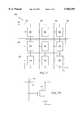
- FIG. 6is a schematic diagram of an SRAM array having a plurality of memory cells arranged in rows and columns;
- FIG. 6Ais a schematic diagram of a representative memory cell of the SRAM array of FIG. 6 with the patterned interconnect structure of FIG. 3;
- FIG. 7is a schematic diagram of a DRAM array having a plurality of memory cells arranged in rows and columns;
- FIG. 7Ais a schematic diagram of a representative memory cell of the DRAM array of FIG. 7 with the patterned interconnect structure of FIG. 3;
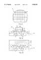
- FIG. 8is a top view of a wafer having the patterned interconnect structure of FIG. 3;
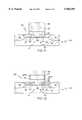
- FIG. 9is an enlarged, sectioned side view depicting the formation of a nitride layer encapsulating a portion of the patterned interconnect structure of FIG. 3;
- FIGS. 10 and 11are enlarged, sectioned side views depicting the formation of a patterned interconnect structure for a MOSFET according to an another aspect of the present invention.
- FIG. 12is an enlarged, sectioned side view depicting the formation of a nitride layer encapsulating a portion of the patterned interconnect structure of FIG. 11.
- the substrate assembly 10comprises a semiconductor layer 12, which is silicon in the illustrated embodiment, and may also include additional layers or structures which define active or operable portions of semiconductor devices (not shown).
- the semiconductor layer 12 of the substrate assembly 10may be formed on insulating material, sapphire or another base material.
- the semiconductor layer 12is doped with impurities to form a semiconductor of a first/p-type conductivity, or a second/n-type conductivity.
- MOSFETmetal oxide semiconductor field effect transistor
- the term MOSFETis a generic term for any field effect transistor in which a conductive material is formed over the gate insulating material of a field effect transistor.
- the conductive materialmay be metallic, conductive polysilicon or a similar conductive material.
- Polysiliconis typically used as the conductive material with MOSFETs having self-aligned gates to form the contact of the gate.
- titanium silicideis a material commonly used to form an interconnect with polysilicon. While the method of the present invention is described in conjunction with polysilicon as part of the gate structure of a MOSFET having a self-aligned gate, the method is suitable for any interconnect structure comprising polysilicon as part of the contact.
- the MOSFET 14 having a self-aligned gate (G)may be formed in accordance with the process described in copending application, U.S. Ser. No. 08/858,772, (Attorney Docket No. MIO 010 PA), A METHOD OF FORMING A FIELD EFFECT TRANSISTOR HAVING A SELF-ALIGNED GATE, filed May 20, 1997, by Donahue et al., herein incorporated by reference.
- the MOSFET 14is isolated by a pair of field oxide regions 16 between which a source 18 and a drain 20 are formed.
- a conductive layer 22contacts the source 18 and the drain 20 and defines the gate (G) of the MOSFET 14.
- a gate oxide layer 24is formed over semiconductor layer 12 and in conjunction with the conductive layer 22 defines the critical dimension for the self-aligned gate (G).
- a layer of polysilicon 26is formed over the semiconductor layer 12 by any conventional deposition technique, such as chemical vapor deposition (CVD) at a temperature ranging from about 600° C. to about 700° C., and typically from about 625° C. to about 650° C., for a predetermined period of time, to a thickness ranging from about 500 Angstroms to about 1500 Angstroms, and preferably about 1000 Angstroms.
- CVDchemical vapor deposition
- Silane gasSiH 4
- dichlorosilaneSiCl 2 H 2
- the layer of polysilicon 26must be doped to increase its conductivity and to also provide a good ohmic contact.
- phosphorous in the form of PH 3is used as a dopant due to its high solubility in silicon.
- the layer of polysilicon 26may be doped during the polysilicon deposition or after the layer 26 is formed by diffusion or ion implantation.
- a layer of titanium silicide 28is formed over the layer of polysilicon 26 to a thickness ranging from about 1000 Angstroms to about 2000 Angstroms, and preferably about 1500 Angstroms.
- the layer of titanium silicide 28is formed using any conventional deposition technique, such as through CVD in which titanium tetrachloride (TiCl 4 ) is combined with SiH 4 or SiCl 2 H 2 at a temperature ranging from about 500° C. to about 900° C., and preferably about 700° C. for a predetermined period of time, or through physical vapor deposition (PVD) in which titanium is sputtered on the layer of polysilicon 26 at a temperature ranging from about 300° C. to about 500° C. for a predetermined period of time.
- CVDchemical vapor deposition
- the annealmay be performed in an anneal furnace or a rapid thermal processor (RTP).
- the annealis performed in an oxygen free environment to prevent the formation of any undesired oxide layer.
- the layers of polysilicon 26 and titanium silicide 28are patterned using standard photolithographic masking and etching to form a patterned structure 30.
- the patterned structure 30may take the form of a gate structure for the transistor 14, a local interconnect for connecting the gates of two or more transistors 14, shown schematically in FIG. 4, or as an interconnect for connecting the gates of a plurality of transistors 14 in an integrated circuit 32, shown schematically in FIG. 5.
- the patterned structure 30may also be used in a typical static random access memory (SRAM) array 34 or in a typical dynamic random access memory (DRAM) array 36, as shown in FIGS. 6 and 7.
- the SRAM array 34 and the DRAM array 36comprise a plurality of memory cells 38 arranged in rows and columns.
- Each of the memory cells 38also comprise at least one transistor 14.
- each of the memory cells 38 of the SRAM array 34comprise a pair of access transistors 14, the gates of which are coupled to a respective row line 40 via the patterned structure 30 of FIG. 3.
- each of the memory cells 38 of the DRAM array 36comprise a switch transistor 14, the gate of which is coupled to a respective word line 42 via the patterned structure 30 of FIG. 3.
- the configuration of the patterned structure 30is dependent, in part, on the desired interconnection of the gates of the transistors 14 as well as the interconnection of the sources and drains of the transistors 14. It should also be apparent that other devices within the integrated circuit 32, the SRAM array 34 and the DRAM array 36, such as external contacts, other FET transistors, bipolar transistors, resistors, capacitors, and the like, may be interconnected via the patterned structure 30.
- the patterned structure 30may also be used in the fabrication of a wafer W as shown in FIG. 8.
- the wafer Wincludes a plurality of individual dies 43. Wafer masks (not shown) are used to apply a desired circuit structure on each of the individual dies 43.
- the desired circuit structuremay comprise any of the above described structures, i.e. the integrated circuit 32, the SRAM array 34 or the DRAM array 36, with the appropriate patterned structure 30.
- the wafer Wis processed using standard wafer fabrication techniques.
- an outer or exposed portion 28A of the layer of titanium silicide 28is nitrified to form a layer of titanium nitride 44 to a thickness ranging from about 50 Angstroms to about 200 Angstroms, and preferably about 150 Angstroms.
- the layer of titanium nitride 44is formed by exposing the patterned structure 30 to a composition of reactive ambient of nitrogen, such as ammonia (NH 3 ), hydrazine (N 2 H 4 ) or a plasma of nitrogen gas (N 2 ), at a temperature ranging from about 500° C. to about 800° C., and preferably about 650° C., for a predetermined period of time.
- This high temperature reactionmay be performed in an annealing furnace or a RTP.
- the environmentmust also be oxygen-free to prevent the formation of an undesired oxide layer.
- the layer of titanium nitride 44encapsulates the layer of titanium silicide 28 and increases the chemical and thermal stability of the patterned structure 30. Titanium nitride is more stable than titanium silicide and does not readily oxidize. The layer of titanium nitride provides an effective chemical barrier to prevent the diffusion of oxygen and other elements across the titanium nitride/titanium silicide interface. Titanium nitride also has a relatively low resistance and does not adversely affect the conductivity of the patterned structure/interconnect 30. The layer of titanium nitride 44 also increases the thermal stability of the patterned structure 30 making the layer of titanium silicide 28 more resistant to agglomeration.
- an insulating layer 46is formed over the layer of titanium silicide 28, as shown in FIG. 10, to increase the eventual height of the patterned structure 30.
- the insulating layer 46may comprise titanium dioxide, silicon dioxide insulation material, boron glass, phosphorus glass, boron/phosphorus glass, or any other material which is an insulator. The thickness of the insulating layer 46 is dependent on the desired height of the patterned structure 30.
- the exposed sides 28B of the layer of titanium silicide 28are nitrified to form the layer of titanium nitride 44 in the same manner as described above.
- the layer of titanium nitride 44encapsulates the exposed sides 28B of the layer of titanium silicide 28, thereby increasing the chemical and thermal stability of the patterned structure 30 in the same manner as described above.
Landscapes
- Engineering & Computer Science (AREA)
- Physics & Mathematics (AREA)
- Condensed Matter Physics & Semiconductors (AREA)
- General Physics & Mathematics (AREA)
- Manufacturing & Machinery (AREA)
- Computer Hardware Design (AREA)
- Microelectronics & Electronic Packaging (AREA)
- Power Engineering (AREA)
- Internal Circuitry In Semiconductor Integrated Circuit Devices (AREA)
- Electrodes Of Semiconductors (AREA)
Abstract
Description
Claims (23)
Priority Applications (1)
| Application Number | Priority Date | Filing Date | Title |
|---|---|---|---|
| US08/880,275US5960303A (en) | 1997-06-23 | 1997-06-23 | Process of forming titanium silicide interconnects |
Applications Claiming Priority (1)
| Application Number | Priority Date | Filing Date | Title |
|---|---|---|---|
| US08/880,275US5960303A (en) | 1997-06-23 | 1997-06-23 | Process of forming titanium silicide interconnects |
Publications (1)
| Publication Number | Publication Date |
|---|---|
| US5960303Atrue US5960303A (en) | 1999-09-28 |
Family
ID=25375931
Family Applications (1)
| Application Number | Title | Priority Date | Filing Date |
|---|---|---|---|
| US08/880,275Expired - LifetimeUS5960303A (en) | 1997-06-23 | 1997-06-23 | Process of forming titanium silicide interconnects |
Country Status (1)
| Country | Link |
|---|---|
| US (1) | US5960303A (en) |
Cited By (10)
| Publication number | Priority date | Publication date | Assignee | Title |
|---|---|---|---|---|
| US6166425A (en)* | 1997-07-16 | 2000-12-26 | Nec Corporation | Semiconductor device having a resistance element with a reduced area |
| US6214714B1 (en)* | 1999-06-25 | 2001-04-10 | Applied Materials, Inc. | Method of titanium/titanium nitride integration |
| US6218274B1 (en)* | 1997-10-28 | 2001-04-17 | Sony Corporation | Semiconductor device and manufacturing method thereof |
| US6218238B1 (en)* | 1998-09-11 | 2001-04-17 | United Microelectronics Corp. | Method of fabricating DRAM capacitor |
| US6391760B1 (en)* | 1998-12-08 | 2002-05-21 | United Microelectronics Corp. | Method of fabricating local interconnect |
| US6455906B2 (en)* | 1999-08-30 | 2002-09-24 | Micron Technology, Inc. | Gate stack structure with conductive silicide segment that has substantially etched nitride and/or oxynitride defects protruding from its sidewalls |
| US6524952B1 (en) | 1999-06-25 | 2003-02-25 | Applied Materials, Inc. | Method of forming a titanium silicide layer on a substrate |
| US6607979B1 (en)* | 1999-09-30 | 2003-08-19 | Nec Corporation | Semiconductor device and method of producing the same |
| US20040061184A1 (en)* | 2002-09-30 | 2004-04-01 | Jiong-Ping Lu | Nickel silicide - silicon nitride adhesion through surface passivation |
| US20090309142A1 (en)* | 2008-06-11 | 2009-12-17 | Micron Technology, Inc. | Imager devices having differing gate stack sidewall spacers, method for forming such imager devices, and systems including such imager devices |
Citations (10)
| Publication number | Priority date | Publication date | Assignee | Title |
|---|---|---|---|---|
| US5202287A (en)* | 1989-01-06 | 1993-04-13 | International Business Machines Corporation | Method for a two step selective deposition of refractory metals utilizing SiH4 reduction and H2 reduction |
| US5236868A (en)* | 1990-04-20 | 1993-08-17 | Applied Materials, Inc. | Formation of titanium nitride on semiconductor wafer by reaction of titanium with nitrogen-bearing gas in an integrated processing system |
| US5250467A (en)* | 1991-03-29 | 1993-10-05 | Applied Materials, Inc. | Method for forming low resistance and low defect density tungsten contacts to silicon semiconductor wafer |
| US5272666A (en)* | 1991-10-18 | 1993-12-21 | Lattice Semiconductor Corporation | Programmable semiconductor antifuse structure and method of fabricating |
| US5275715A (en)* | 1992-01-23 | 1994-01-04 | Micron Technology Inc. | Electroplating process for enhancing the conformality of titanium and titanium nitride films in the manufacture of integrated circuits and structures produced thereby |
| US5360996A (en)* | 1991-07-24 | 1994-11-01 | Applied Materials, Inc. | Titanium nitride/titanium silicide multiple layer barrier with preferential (111) crystallographic orientation on titanium nitride surface |
| US5365111A (en)* | 1992-12-23 | 1994-11-15 | Advanced Micro Devices, Inc. | Stable local interconnect/active area silicide structure for VLSI applications |
| US5483104A (en)* | 1990-01-12 | 1996-01-09 | Paradigm Technology, Inc. | Self-aligning contact and interconnect structure |
| US5504038A (en)* | 1995-05-25 | 1996-04-02 | United Microelectronics Corporation | Method for selective tungsten sidewall and bottom contact formation |
| US5545592A (en)* | 1995-02-24 | 1996-08-13 | Advanced Micro Devices, Inc. | Nitrogen treatment for metal-silicide contact |
- 1997
- 1997-06-23USUS08/880,275patent/US5960303A/ennot_activeExpired - Lifetime
Patent Citations (11)
| Publication number | Priority date | Publication date | Assignee | Title |
|---|---|---|---|---|
| US5202287A (en)* | 1989-01-06 | 1993-04-13 | International Business Machines Corporation | Method for a two step selective deposition of refractory metals utilizing SiH4 reduction and H2 reduction |
| US5483104A (en)* | 1990-01-12 | 1996-01-09 | Paradigm Technology, Inc. | Self-aligning contact and interconnect structure |
| US5236868A (en)* | 1990-04-20 | 1993-08-17 | Applied Materials, Inc. | Formation of titanium nitride on semiconductor wafer by reaction of titanium with nitrogen-bearing gas in an integrated processing system |
| US5250467A (en)* | 1991-03-29 | 1993-10-05 | Applied Materials, Inc. | Method for forming low resistance and low defect density tungsten contacts to silicon semiconductor wafer |
| US5360996A (en)* | 1991-07-24 | 1994-11-01 | Applied Materials, Inc. | Titanium nitride/titanium silicide multiple layer barrier with preferential (111) crystallographic orientation on titanium nitride surface |
| US5272666A (en)* | 1991-10-18 | 1993-12-21 | Lattice Semiconductor Corporation | Programmable semiconductor antifuse structure and method of fabricating |
| US5275715A (en)* | 1992-01-23 | 1994-01-04 | Micron Technology Inc. | Electroplating process for enhancing the conformality of titanium and titanium nitride films in the manufacture of integrated circuits and structures produced thereby |
| US5365111A (en)* | 1992-12-23 | 1994-11-15 | Advanced Micro Devices, Inc. | Stable local interconnect/active area silicide structure for VLSI applications |
| US5451545A (en)* | 1992-12-23 | 1995-09-19 | Advanced Micro Devices, Inc. | Process for forming stable local interconnect/active area silicide structure VLSI applications |
| US5545592A (en)* | 1995-02-24 | 1996-08-13 | Advanced Micro Devices, Inc. | Nitrogen treatment for metal-silicide contact |
| US5504038A (en)* | 1995-05-25 | 1996-04-02 | United Microelectronics Corporation | Method for selective tungsten sidewall and bottom contact formation |
Cited By (22)
| Publication number | Priority date | Publication date | Assignee | Title |
|---|---|---|---|---|
| US6166425A (en)* | 1997-07-16 | 2000-12-26 | Nec Corporation | Semiconductor device having a resistance element with a reduced area |
| US6218274B1 (en)* | 1997-10-28 | 2001-04-17 | Sony Corporation | Semiconductor device and manufacturing method thereof |
| US6218238B1 (en)* | 1998-09-11 | 2001-04-17 | United Microelectronics Corp. | Method of fabricating DRAM capacitor |
| US6391760B1 (en)* | 1998-12-08 | 2002-05-21 | United Microelectronics Corp. | Method of fabricating local interconnect |
| US6524952B1 (en) | 1999-06-25 | 2003-02-25 | Applied Materials, Inc. | Method of forming a titanium silicide layer on a substrate |
| US6214714B1 (en)* | 1999-06-25 | 2001-04-10 | Applied Materials, Inc. | Method of titanium/titanium nitride integration |
| US6326690B2 (en) | 1999-06-25 | 2001-12-04 | Applied Materials, Inc. | Method of titanium/titanium nitride integration |
| US6686275B2 (en) | 1999-08-30 | 2004-02-03 | Micron Technology, Inc. | Method of selectively removing metal nitride or metal oxynitride extrusions from a semmiconductor structure |
| US6743720B2 (en) | 1999-08-30 | 2004-06-01 | Micron Technology, Inc. | Method of manufacturing a portion of a memory by selectively etching to remove metal nitride or metal oxynitride extrusions |
| US7211200B2 (en) | 1999-08-30 | 2007-05-01 | Micron Technology, Inc. | Manufacture and cleaning of a semiconductor |
| US6455906B2 (en)* | 1999-08-30 | 2002-09-24 | Micron Technology, Inc. | Gate stack structure with conductive silicide segment that has substantially etched nitride and/or oxynitride defects protruding from its sidewalls |
| US6693354B2 (en) | 1999-08-30 | 2004-02-17 | Micron Technology Inc. | Semiconductor structure with substantially etched nitride defects protruding therefrom |
| US6703303B2 (en) | 1999-08-30 | 2004-03-09 | Micron Technology Inc. | Method of manufacturing a portion of a memory |
| US6933580B2 (en) | 1999-08-30 | 2005-08-23 | Micron Technology, Inc. | Semiconductor structure with substantially etched oxynitride defects protruding therefrom |
| US20030151021A1 (en)* | 1999-08-30 | 2003-08-14 | Gary Chen | Manufacture and cleaning of a semiconductor |
| US20040124530A1 (en)* | 1999-08-30 | 2004-07-01 | Gary Chen | Semiconductor structure with substantially etched oxynitride defects protruding therefrom |
| US6607979B1 (en)* | 1999-09-30 | 2003-08-19 | Nec Corporation | Semiconductor device and method of producing the same |
| US6831008B2 (en)* | 2002-09-30 | 2004-12-14 | Texas Instruments Incorporated | Nickel silicide—silicon nitride adhesion through surface passivation |
| US20050090087A1 (en)* | 2002-09-30 | 2005-04-28 | Jiong-Ping Lu | Nickel silicide - silicon nitride adhesion through surface passivation |
| US20040061184A1 (en)* | 2002-09-30 | 2004-04-01 | Jiong-Ping Lu | Nickel silicide - silicon nitride adhesion through surface passivation |
| US20090309142A1 (en)* | 2008-06-11 | 2009-12-17 | Micron Technology, Inc. | Imager devices having differing gate stack sidewall spacers, method for forming such imager devices, and systems including such imager devices |
| US8129764B2 (en) | 2008-06-11 | 2012-03-06 | Aptina Imaging Corporation | Imager devices having differing gate stack sidewall spacers, method for forming such imager devices, and systems including such imager devices |
Similar Documents
| Publication | Publication Date | Title |
|---|---|---|
| US8003526B2 (en) | Low resistance metal silicide local interconnects and a method of making | |
| US5767004A (en) | Method for forming a low impurity diffusion polysilicon layer | |
| US6524953B1 (en) | Asymmetric, double-sided self-aligned silicide and method of forming the same | |
| US5326722A (en) | Polysilicon contact | |
| US7316954B2 (en) | Methods of fabricating integrated circuit devices that utilize doped poly-Si1−xGex conductive plugs as interconnects | |
| JP3688734B2 (en) | Method of manufacturing part of integrated circuit and structure thereof | |
| EP0503904A2 (en) | Contact structure of an interconnection layer placed on a surface having steps and SRAM having a multilayer interconnection and manufacturing method thereof | |
| US6281101B1 (en) | Process of forming metal silicide interconnects | |
| US4985746A (en) | Semiconductor device and method of production | |
| KR100192017B1 (en) | Manufacturing Method of Semiconductor Device | |
| JP3246442B2 (en) | Method for manufacturing semiconductor device | |
| US5960303A (en) | Process of forming titanium silicide interconnects | |
| KR970077674A (en) | Manufacturing method of semiconductor integrated circuit device | |
| EP0647969A1 (en) | Method of forming contacts in the memory region and the peripheral region of an IC | |
| US4859278A (en) | Fabrication of high resistive loads utilizing a single level polycide process | |
| US5622884A (en) | Method for manufacturing a semiconductor memory cell and a polysilicon load resistor of the semiconductor memory cell | |
| US5190886A (en) | Semiconductor device and method of production | |
| KR0161380B1 (en) | Transistor of semiconductor device and manufacturing method thereof | |
| US20010023978A1 (en) | Semiconductor device and manufacturing method thereof | |
| KR0144413B1 (en) | Semiconductor device and manufacturing method | |
| KR100351895B1 (en) | Method for forming bitline in semiconductor device | |
| US6197672B1 (en) | Method for forming polycide dual gate | |
| JPH08107153A (en) | Manufacture of semiconductor device | |
| JPH02203565A (en) | Semiconductor device and its manufacture | |
| US20010003671A1 (en) | Method for manufacturing semiconductor device having refractory metal silicide film |
Legal Events
| Date | Code | Title | Description |
|---|---|---|---|
| AS | Assignment | Owner name:MICRON TECHNOLOGY, INC., IDAHO Free format text:ASSIGNMENT OF ASSIGNORS INTEREST;ASSIGNOR:HILL, CHRISTOPHER W.;REEL/FRAME:008614/0267 Effective date:19970619 | |
| STCF | Information on status: patent grant | Free format text:PATENTED CASE | |
| CC | Certificate of correction | ||
| FPAY | Fee payment | Year of fee payment:4 | |
| FPAY | Fee payment | Year of fee payment:8 | |
| FPAY | Fee payment | Year of fee payment:12 | |
| AS | Assignment | Owner name:U.S. BANK NATIONAL ASSOCIATION, AS COLLATERAL AGENT, CALIFORNIA Free format text:SECURITY INTEREST;ASSIGNOR:MICRON TECHNOLOGY, INC.;REEL/FRAME:038669/0001 Effective date:20160426 Owner name:U.S. BANK NATIONAL ASSOCIATION, AS COLLATERAL AGEN Free format text:SECURITY INTEREST;ASSIGNOR:MICRON TECHNOLOGY, INC.;REEL/FRAME:038669/0001 Effective date:20160426 | |
| AS | Assignment | Owner name:MORGAN STANLEY SENIOR FUNDING, INC., AS COLLATERAL AGENT, MARYLAND Free format text:PATENT SECURITY AGREEMENT;ASSIGNOR:MICRON TECHNOLOGY, INC.;REEL/FRAME:038954/0001 Effective date:20160426 Owner name:MORGAN STANLEY SENIOR FUNDING, INC., AS COLLATERAL Free format text:PATENT SECURITY AGREEMENT;ASSIGNOR:MICRON TECHNOLOGY, INC.;REEL/FRAME:038954/0001 Effective date:20160426 | |
| AS | Assignment | Owner name:U.S. BANK NATIONAL ASSOCIATION, AS COLLATERAL AGENT, CALIFORNIA Free format text:CORRECTIVE ASSIGNMENT TO CORRECT THE REPLACE ERRONEOUSLY FILED PATENT #7358718 WITH THE CORRECT PATENT #7358178 PREVIOUSLY RECORDED ON REEL 038669 FRAME 0001. ASSIGNOR(S) HEREBY CONFIRMS THE SECURITY INTEREST;ASSIGNOR:MICRON TECHNOLOGY, INC.;REEL/FRAME:043079/0001 Effective date:20160426 Owner name:U.S. BANK NATIONAL ASSOCIATION, AS COLLATERAL AGEN Free format text:CORRECTIVE ASSIGNMENT TO CORRECT THE REPLACE ERRONEOUSLY FILED PATENT #7358718 WITH THE CORRECT PATENT #7358178 PREVIOUSLY RECORDED ON REEL 038669 FRAME 0001. ASSIGNOR(S) HEREBY CONFIRMS THE SECURITY INTEREST;ASSIGNOR:MICRON TECHNOLOGY, INC.;REEL/FRAME:043079/0001 Effective date:20160426 | |
| AS | Assignment | Owner name:MICRON TECHNOLOGY, INC., IDAHO Free format text:RELEASE BY SECURED PARTY;ASSIGNOR:U.S. BANK NATIONAL ASSOCIATION, AS COLLATERAL AGENT;REEL/FRAME:047243/0001 Effective date:20180629 | |
| AS | Assignment | Owner name:MICRON TECHNOLOGY, INC., IDAHO Free format text:RELEASE BY SECURED PARTY;ASSIGNOR:MORGAN STANLEY SENIOR FUNDING, INC., AS COLLATERAL AGENT;REEL/FRAME:050937/0001 Effective date:20190731 |