US5959923A - Digital computer having a system for sequentially refreshing an expandable dynamic RAM memory circuit - Google Patents
Digital computer having a system for sequentially refreshing an expandable dynamic RAM memory circuitDownload PDFInfo
- Publication number
- US5959923A US5959923AUS08/058,822US5882293AUS5959923AUS 5959923 AUS5959923 AUS 5959923AUS 5882293 AUS5882293 AUS 5882293AUS 5959923 AUS5959923 AUS 5959923A
- Authority
- US
- United States
- Prior art keywords
- memory
- refresh
- memory banks
- slots
- group
- Prior art date
- Legal status (The legal status is an assumption and is not a legal conclusion. Google has not performed a legal analysis and makes no representation as to the accuracy of the status listed.)
- Expired - Lifetime
Links
Images


Classifications
- G—PHYSICS
- G11—INFORMATION STORAGE
- G11C—STATIC STORES
- G11C11/00—Digital stores characterised by the use of particular electric or magnetic storage elements; Storage elements therefor
- G11C11/21—Digital stores characterised by the use of particular electric or magnetic storage elements; Storage elements therefor using electric elements
- G11C11/34—Digital stores characterised by the use of particular electric or magnetic storage elements; Storage elements therefor using electric elements using semiconductor devices
- G11C11/40—Digital stores characterised by the use of particular electric or magnetic storage elements; Storage elements therefor using electric elements using semiconductor devices using transistors
- G11C11/401—Digital stores characterised by the use of particular electric or magnetic storage elements; Storage elements therefor using electric elements using semiconductor devices using transistors forming cells needing refreshing or charge regeneration, i.e. dynamic cells
- G11C11/406—Management or control of the refreshing or charge-regeneration cycles
Definitions
- the inventionrelates to computer memory systems and, more particularly, to the refresh of DRAM storage elements in such memories.
- Data processing systems for computersuse memory to store information. More specifically, the data processor of a computer stores individual units of information consisting of a specific number of bits representing binary digits at specific locations within a memory unit. The locations within the memory where data bits are stored, are specified by addresses. Each address consists of a specific number of bits and the total number of bits available for address information defines the total number of memory locations that can be addressed within the computer. The total number of addressable memory locations, in turn, provides a limit to the amount of information that can be stored and accessed by the data processor. This limitation in memory limits the capability of the data processor in performing its data processing functions.
- ROMread only memory
- RAMrandom access memory
- a typical RAMconsists of a plurality of memory cells, an address decoder, read/write control circuitry and a memory output register. While there are many variations in the structure of and interconnection between the basic elements of RAMs which are utilized to separate different RAM designs into numerous classifications, RAMs may be separated into two distinct types based on the structure of the memory cells used in the memory unit--the "static" RAM (or “SRAM”) and the “dynamic” RAM (or “DRAM”).
- SRAMstatic RAM
- DRAMdynamic RAM
- each memory cell of a DRAMincludes a microscopic "storage" capacitor consisting of two conductive layers separated by an insulator.
- the memory cell of a DRAMstores a single bit of information in the microscopic capacitor as the presence or absence of an electric charge in that capacitor.
- a charged capacitorgenerally represents a "1”
- a discharged capacitorgenerally represents a "0".
- a single transistoris used to control charging the storage capacitor.
- each memory cellSince the electric charge stored in the storage capacitor of a memory cell will gradually leak away, the stored information must be periodically rewritten into the cell before the charge completely leaks out. This periodic rewriting of the information previously stored in the memory cell is called "refreshing" the memory.
- the frequency at which a memory cell must be refreshedvaries depending on the rate of leakage in the control transistor. In a typical DRAM, each memory cell must be refreshed every two, four or eight milliseconds.
- the DRAMis often used due to certain advantages over the SRAM. For example, because the DRAM requires only a single control transistor while the SRAM requires 4 to 6 transistors, the DRAM occupies a much smaller area on the silicon substrate than the SRAM and is less expensive to manufacture. Furthermore, the DRAM consumes less power than a SRAM. Thus, DRAMS are particularly attractive in most microcomputer systems where space and power consumption are at a premium.
- both memory accessi.e. writing to or reading from a memory cell
- refresh operationsare controlled by a combination of a pair of signals called a row address strobe (or "RAS") signal and a column address strobe (or "CAS”) signal, respectively.
- RASrow address strobe
- CAScolumn address strobe
- the RAS and CAS signalsare used to select the particular memory cell to be accessed.
- Some DRAMsalso require manipulation of both the RAS and CAS signals to perform a refresh cycle. Other DRAMs may be refreshed by activating only the RAS signal.
- any attempt to simultaneously refresh all of the DRAM SIMMSwould require a substantial amount of power to simultaneously provide a RAS signal to every row of every memory bank in the memory unit. Since there is a plurality of memory banks, the refresh power requirement for refreshing all memory banks simultaneously would generate a large power surge, resulting in possible electromagnetic interference problems, as well as require an excessive amount of power service.
- the staggered refresh circuitwould generate a row address to all of the memory banks and generate a RAS pulse to instruct the DRAMs to latch the row address to each of the banks in turn.
- any number of memory slots included in a memory unitmay have a memory bank installed therein.
- a systemincorporates a memory unit having eight slots which are each capable of having a memory bank installed therein, and if only four of the slots actually have memory banks installed, a refresh cycle which sequentially issues a memory refresh signal to each slot would be inefficient. It would be preferable that the memory refresh sequence would issue refresh signals only to those slots in which memory banks had been installed. Not only would such a capability improve the efficiency of the refresh sequence, it would improve access to the memory unit as well.
- a flexible memory refresh sequencewould also be advantageous when the memory unit of a computer is upgraded or otherwise modified after the initial configuration of the computer system.
- a memory unit consisting of a single memory cardmay initially have memory banks installed in only four out of the eight available slots typically provided on a memory card. Increased memory requirements in the computer system may later require that additional memory banks be installed.
- the memory refresh sequenceis designed based upon the initial memory configuration, changes such as memory upgrades would require resequencing of the refresh signals in order to keep them operating at optimum efficiency.
- it would be desirable to provide a refresh sequence controllerwhich would maximize the ease with which the refresh sequence can be modified so that efficiency of the refresh sequence is maximized for any particular memory unit configuration.
- the system of the present inventionis a digital computer which includes a computer system having at least one memory unit that may comprise a memory card with a plurality of slots each capable of receiving a dynamic random access memory bank therein and which includes a memory refresh system for controlling the refresh of the memory banks.
- the memory refresh systemincludes an independent memory refresh sequence controller for each memory card included in the memory unit and means for sequentially refreshing the memory banks by the generation of refresh signals. Each memory refresh sequence controller selectively controls the order in which the memory banks installed on the corresponding memory card are refreshed such that the refresh sequence for the memory unit is operated efficiently.
- each memory refresh sequence controllercontrols at least one multi-stage shift register for issuing refresh signals to memory banks installed on the corresponding memory card and at least one multi-stage shift register for providing wait cycles during which refresh signals are being generated by other memory refresh circuits included in the memory refresh system.
- Each memory refresh controllerincludes a series of inputs which vary depending on the configuration of the memory unit installed in the particular computer system so that the refresh sequence of each independent memory refresh controller varies depending on the configuration of the installed memory unit.
- the present inventionis a digital computer which includes a system for controlling the refresh operation of a memory unit comprised of at least one memory card having a series of dynamic RAM memory banks installed therein.
- the systemincludes means for sequentially refreshing the dynamic RAM memory banks and means for selectively controlling the order in which the dynamic RAM memory banks are refreshed.
- the selective control meansadjusts the order in which the memory banks are refreshed based on the number of memory.
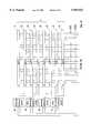
- FIG. 1is a block diagram of a computer system having a DRAM memory refresh system constructed in accordance with the teachings of the present invention
- FIG. 2is a schematic diagram illustrating the interconnection of the memory refresh system and a memory unit comprised of a pair of memory cards;
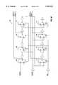
- FIG. 3is a schematic diagram of the memory refresh module of the memory refresh system of FIG. 2;
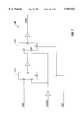
- FIG. 4is a schematic diagram of the memory refresh sequence controller of the refresh signal generating means of FIG. 3;
- FIG. 5Ais a schematic diagram of a first four stage shift register for generating refresh signals RAS 0-3 included as part of the refresh signal generating means of FIG. 3;
- FIG. 5Bis a schematic diagram of a second four stage shift register for generating refresh signals RAS 4-7 included as part of the refresh signal generating means of FIG. 3;
- FIG. 6Ais a schematic diagram of a first four stary shift register for generating wait cycles included as part of the refresh signal generating means of FIG. 3;
- FIG. 6Bis a schematic diagram of a second four stage shift register for generating wait cycles included as part of the refresh signal generating means of FIG. 3;
- FIG. 7is a schematic diagram of the RAS signal synchronizing circuit of FIG. 3.
- a data processor for use in a digital computer systemmay be comprised of any number of interconnected components.
- a computer system incorporating the memory refresh modulewhich is the subject of the present invention may include a data processor 6 comprised of a microprocessor 10 such as a Model 80386 microprocessor manufactured by Intel Corporation of Santa Clara, Calif., a first coprocessor 12 such as a Model 80387 coprocessor, also manufactured by Intel Corporation and a second coprocessor 14 such as a Model 3167 coprocessor manufactured by the Weitek Company.
- the microprocessor 10, first coprocessor 12 and second coprocessor 14are interconnected with each other via an address, data and control bus 16 of conventional design.
- Data/ECCdata flow and error correction code
- Control and address signals from the data processor 6 to the memory unit 8are transmitted by a memory and bus (or “memory/bus") controller 20.
- the data/ECC controller 18 and the memory/bus controller 20transmit and receive memory data, memory address signals and memory control signals to and from the memory unit 8 via the memory connector 22.
- the memory unit 8is comprised of at least one memory card having a series of slots provided thereon for receiving memory banks 26a-26h comprised of DRAM memory components.
- Datais stored in 64 bit blocks, but because the processor and ECC circuitry only handle 32 bit double words, interleaving is used to handle the entry and retrieval of each pair of 32 bit double words comprising a 64 bit block (actually each 32 bit data word comprises 39 bits, since with ECC each word also includes 7 syndrome bits, so that a total 78 bit block is formed) in the form of 2 interleaved banks of 32 bit double words, one odd and one even.
- Each interleave controller 24a-24dmultiplexes eight bits of data (exclusive of parity or ECC syndrome bits) between the memory connector 22 and the memory banks 26a-26h. In other words, for a read command, each interleave controllers 24a-24d access eight even data bits from an even memory bank and eight odd data bits from an odd memory bank.
- a RAS, CAS and refresh controller 32(which includes the memory refresh modules 34a and 34b) receives encoded control signals from the memory connector 22 and, in turn, transmits decoded control signals, i.e. the previously discussed RAS and CAS signals, to the memory banks 26a-26h as they are needed to access a data location.
- the RAS, CAS and refresh controller 32also generates refresh signals to the memory banks 26a-26h as is more fully discussed below.
- the memory unit 8is comprised of a pair of memory cards 8a and 8b, respectively.
- Each memory card 8a, 8bhas a series of eight slots, into each of which a memory bank has been installed therein.
- the memory unit 8includes a series of sixteen memory banks herein identified as memory banks 0-15 evenly divided between the memory cards 8a, 8b.
- each memory bank 0-15is comprised of one side of a double-sided SIMM.
- the memory unit 8may be comprised of one, two or more memory cards and further that the memory banks 26a-26h installed on said memory cards may be comprised of single-sided SIMMs, double-sided SIMMs or any combination thereof. It is further contemplated that the memory refresh sequence generated by the memory refresh modules 34a and 34b included as part of the RAS, CAS and refresh controller 32 may be easily modified such that numerous combinations of the number of memory cards and/or combinations of single and/or double sided SIMMs may be installed in the memory unit 8 without detrimentally affecting the efficiency of the memory refresh sequence.
- FIG. 1illustrates a single RAS, CAS and refresh controller 32 which includes a single memory refresh means for refreshing a memory unit comprised of a single memory card, a memory unit comprised of a pair of memory cards may be refreshed by the installation of a second RAS, CAS and refresh controller 32 which includes a second memory refresh means.
- Each memory refresh module 34a, 34b of a single memory refresh meanshas five inputs: RAS, CLOCK, REF, A8 13 16 ⁇ and FIRST which, as described below, will generate a series of refresh signals RAS 0-7 to each series of memory banks associated therewith.
- a RAS signalis generated by the memory/bus controller 20 by conventional means and is transmitted to the corresponding memory refresh modules 34a or 34b via the memory connector 22 and the RAS input.
- the RAS signalis asserted at the beginning of the refresh sequence and stays high a sufficient time to refresh a DRAM. Accordingly, the width of the RAS input pulse will vary depending on the physical characteristics of the DRAMs installed in the memory banks.
- Each memory refresh module 34a, 34balso receives a clocking signal generated by a clock circuit 36.
- the clock circuit 36generates a series of pulses separated by a time period sufficient to permit, as is more fully described below, a shift register to advance.
- a refresh (or "REF") signalis also generated by the memory/bus controller 20 by conventional means and is transmitted to the corresponding memory refresh modules 34a or 34b via the memory connector 22 and the REF input.
- the REF signalbrings the memory refresh module 34a, 34b out of reset, thereby permitting the refresh sequence to commence. Accordingly, the period of the REF signal is selected to be the same as the period of time after which the DRAMs installed in the memory banks 8a, 8b require refreshing.
- each memory refresh module 34a, 34bThe final two inputs to each memory refresh module 34a, 34b are the A8 -- 16 ⁇ and FIRST input signals FIRST-A and FIRST-B which are selectively tied to a high or low voltage. These inputs vary depending upon the configuration of the memory unit 8 installed. Depending on the states of the A8 -- 16 ⁇ and the corresponding FIRST input FIRST-A or FIRST-B, the sequence in which the memory banks associated with the memory refresh module 34a, 34b will vary. As a result, the memory refresh module 34a, 34b will modify the memory refresh sequence depending on the particular configuration of the number of memory cards included in the memory unit 8 as well as the number of memory banks installed in each memory card 8a, 8b.
- the A 8 -- 16 ⁇ input to the memory refresh module 34a, 34bindicates whether the memory unit 8 includes one or two memory cards.
- a "1" input on the A8 -- 16 ⁇ inputindicates that the memory unit 8 is comprised of a single memory card 8a or 8b and a "0" on the A8 -- 16 ⁇ input indicates that the memory unit 8 includes both the memory card 8a and the memory card 8b.
- FIRST inputs FIRST-A and FIRST-Bare provided to the memory refresh module 34a, 34b, respectively, to indicate to the respective memory refresh module 34a, 34b whether that refresh controller is controlling refresh in the "low" memory banks (hereby designated as memory banks 0-7 ) corresponding to the memory card 8a or the "high” memory banks (hereby designated as memory banks 8-15 ) corresponding to the memory card 8b.
- Each memory refresh module 34a, 34bhas a series of 8 outputs designated as outputs RAS 0-7 which control the sequential refresh of the memory banks tied to the respective memory refresh module 34a, 34b.
- the order in which the RAS signals are generated and the order in which the memory banks 0-15 are refresheddepends on the states of the A8 -- 16 ⁇ , FIRST-A and FIRST-B signals.
- each memory refresh moduleis such that when A8 -- 16 ⁇ is high, i.e. the memory unit 8 includes only one memory card, the eight RAS outputs of the memory refresh module are generated sequentially, thereby refreshing the corresponding memory banks sequentially.
- A8 -- 16 ⁇goes low, i.e. the memory unit 8 includes a pair of memory cards, the RAS outputs of the memory refresh module 34a, 34b change dramatically.
- wait cycles during which no outputs are producedwill be interspersed between certain RAS outputs of the memory refresh module depending on whether the memory refresh module is refreshing the lower or upper memory banks, thereby changing the sequence that the memory banks are refreshed.
- each memory refresh module 34a, 34butilizes the A8 -- 16 ⁇ and FIRST signals to determine which section of the memory the refresh controller 32 is responsible for. As a result, identical memory refresh modules 34a, 34b may be utilized for both the low and high memory cards without requiring any interconnections between the two.
- the bank refresh order and assignment of bank numbersare selected so that no penalty is paid for using single sided SIMMs.
- the memory refresh module 34a, 34bsequentially refresh only those memory banks actually installed. For example, if the memory unit 8 includes single-sided SIMMs installed in the banks 0, 1, 2, 3 of the memory card 8a and the bank 8 of the memory card 8b, shortening the length of the REF pulse to 5 CLOCK cycles will refresh only those memory banks.
- the memory banks 0, 1, 2, 3 and 8, 9, 10, 11are installed whether single-sided or double-sided SIMMs are utilized.
- the memory banks 4, 5, 6, 7 and 12, 13, 14, 15, on the other hand,are installed only when double-sided SIMMs are utilized. Accordingly, when double-sided SIMMs are installed, the memory refresh module will first sequentially refresh all of the first sides of the SIMMs and then sequentially refresh all of the second sides of the SIMMs. On the other hand, when single-sided SIMMs are installed and the refresh pulse width is shortened by one-half, the memory refresh module generates a refresh sequence comprising only the sequential refresh of all of those memory banks corresponding to the first sides of the SIMMs.
- Each memory refresh module 34a, 34bincludes a RAS synchronizing circuit 38 for synchronizing the RAS signals and the clock pulses; a memory refresh sequence controller 40; a first refresh circuit 42 which transmits refresh signals RAS 0-3 to the memory banks tied to those signals; a second refresh circuit 44 which transmits refresh signals RAS 4-7 to those memory banks tied thereto; and first and second wait circuits 46, 48 for inserting a series of wait cycles where the memory refresh module does not generate a refresh signal to a memory bank.
- wait cyclesare generated by systems having plural memory refresh modules for refreshing a memory unit having plural memory cards such that no two memory refresh modules will be refreshing memory banks simultaneously.
- the memory cards 8a, 8brequire periodic refresh. Refreshing of the memory cards 8a, 8b commences upon the generation of the REF signal by the memory refresh modules 34a, 34b.
- the refresh signalis a pulse of length equal to the time required to refresh a DRAM installed in a memory bank multiplied by the total number of slots 26a-26h which have been filled by memory banks.
- the REF signalremains high during the entire refreshing sequence and goes low between refresh cycles.
- the RAS signalwhich is a pulse of length equal to the time required to refresh a memory bank, is generated by the memory refresh module 34.
- the RAS signalis input to the RAS synchronizing circuit 38 along with a periodic clock pulse (CLOCK) generated by the clock circuit 36 of conventional design.
- the RAS synchronizing circuit 38synchronizes the RAS signal with a clock pulse and outputs a synchronized RAS signal ("SYNC") to the memory refresh sequence controller 40 and the first wait circuit 46.
- the first wait circuit 46outputs a pulse (“FWBU”) to the memory refresh sequence controller 40 after a period of time equal to the length of four RAS pulses have elapsed.
- the FWBU pulsedoesn't matter to the memory refresh sequence controller 40 and, upon receipt of the SYNC pulse, the memory refresh sequence controller 40 generates a signal ("FSHBU") to the first refresh circuit 42 to begin generating RAS pulses to the memory card. If, however the A8 -- 16 ⁇ signal is low and the FIRST signal is high, the memory refresh sequence controller 40 will not generate the FSHBU signal until receiving the FWBU pulse from the first wait circuit 46.
- the first refresh circuit 42generates five sequential pulses of a width equal to a RAS pulse.
- the first four pulses(“RAS 0-3") are transmitted to the memory card for sequentially refreshing three memory banks.
- the fifth pulse(“OUT-5") is transmitted to the memory refresh sequence controller 40 and the second wait circuit 48.
- the second wait circuit 48outputs a pulse ("SWBU”) to the memory refresh sequence controller 40 after a period of time equal to the length of four RAS pulses have elapsed.
- the SWBU pulsedoesn't matter to the memory refresh sequence controller 40 and, upon receipt of the OUT-5 pulse, the memory refresh sequence controller 40 will generate a SSHBU signal to the second refresh circuit 44 to begin generating additional RAS pulses to the memory card. If the A8 -- 16 ⁇ signal is low, however, the FIRST signal doesn't matter and the memory refresh sequence controller 40 will not generate the SSHBU signal until receiving the SWBU pulse from the second wait circuit 48.
- the second refresh circuit 44generates five sequential pulses of a width equal to a RAS pulse.
- the first four pulses(“RAS 4-7") are transmitted to the memory card for sequentially refreshing four memory banks.
- the fifth pulseis left unconnected.
- RAS-7has been transmitted to the memory card, all banks on that memory card have been refreshed and the memory refresh modules 34a, 34b will not generate any additional refresh pulses until the REF signal resets the refresh circuits 42, 44 and the wait circuits 46, 48 by going low, and then going high to indicate the beginning of the next refresh cycle.
- the memory refresh sequence controller 40is comprised of a series of logic gates of conventional design interconnected as herein described. Both the A8 -- 16 ⁇ and FIRST signals are each input into an OR gate 50 and a NOR gate 52.
- the output of the OR gate 50is, in turn, provided as a first input to an AND gate 54 and the SYNC output from the RAS synchronizing circuit 38 is provided as a second input to the AND gate 54.
- the output of the NOR gate 52is provided as a first input to an AND gate 56 and the FWBU output from the first wait circuit 46 is provided as a second input to the AND gate 56.
- the outputs of the AND gates 54, 56are input to a NOR gate 58 and the output of the NOR gate 58, after being inverted by an invertor 60, is the FSHBU signal to be supplied to the first refresh circuit 42 to begin generation of four RAS pulses for refreshing memory banks, either immediately or after four wait cycles, depending on the state of the A8 -- 16 ⁇ and FIRST signals.
- the first refresh circuit 42provides the OUT-5 signal as a first input to an AND gate 62 and the A8 -- 16 ⁇ signal is provided as a second input to the AND gate 62.
- the A8 -- 16-- input, after being inverted by an invertor 64is provided as a first input to an AND gate 66 and the SWBU output from the second wait circuit 48 is provided as a second input to the AND gate 66.
- the outputs of the AND gates 62 and 66are input into a NOR gate 68 and the output of the NOR gate 68, after being inverted by an invertor 70 is provided as the SSHBU input to the second refresh circuit 44.
- the SSHBU signalwill be transmitted to the second refresh circuit 44, thereby beginning the generation of the second set of four RAS pulses for refreshing additional memory banks, either upon receipt of the OUT-5 signal indicating the generation of RAS pulses by the first refresh circuit 42 has been completed, or upon receipt of the SWBU signal indicating that four wait cycles during which a second memory refresh module has generated RAS pulses has been completed, depending on the state of the A8 -- 16 ⁇ signal.
- the first refresh circuit 42is a four-stage shift register comprised of a series of type D latches 50, 52, 54, 56, 58, 60, 62 and 64 tied together in series.
- the CLOCK signalis tied to a clock ("E" or “EN”) terminal of each latch 50-64 and the REF signal is tied to a reset (or "R") terminal of each latch 50-64.
- the FSHBU output of the memory refresh sequence controller 40is tied to a D input of the latch 50.
- each latch 50-62As the Q output of each latch 50-62 is tied to a D input of each successive latch 52-64, the high output from the latch 50 is shifted to the outputs of the latches 52-64 in sequence.
- the RAS-0 signalis provided by the output of latch 50, the RAS-1 signal by the output of the latch 54, the RAS-2 signal by the output of the latch 58 and the RAS-3 signal by the output of the latch 62.
- the output of the latch 64is tied to the memory refresh sequence controller 40 to indicate that the first refresh circuit 42 has generated the appropriate RAS pulses.
- the second refresh circuit 44is a four-stage shift register comprised of a series of type D latches 66, 68, 70, 72, 74, 76, 78 and 80 tied together in series.
- the CLOCK signalis tied to a clock ("E" or "EN") terminal of each latch 66-80 and the REF signal is tied to a reset (or "R") terminal of each latch 66-80.
- the SSHBU output of the memory refresh sequence controller 40is tied to a D input of the latch 66.
- each latch 66-78As a Q output of each latch 66-78 is tied to a D input of each successive latch 68-80, the high output from the latch 66 is shifted to the outputs of the latches 68-80 in sequence.
- the RAS-4 signalis provided by the Q output of the latch 66, the RAS-5 signal by the Q output of the latch 70, the RAS-6 signal by the Q output of the latch 74 and the RAS-7 signal by the Q output of the latch 78.
- the Q output of the latch 80is unconnected.
- the first wait circuit 46is a four-stage shift register comprised of a series of type D latches 82, 84, 86, 88, 90, 92, 94 and 96 tied together in series.
- the CLOCK signalis tied to a clock ("E" or “EN") terminal of each latch 82-96 and the REF signal is tied to a reset (or "R") terminal of each latch 82-96.
- the SYNC output of the RAS synchronizing circuit 38is tied to a D input of the latch 82.
- the first wait circuit 46is constructed identically to the four stage shift registers which comprise the first and second refresh circuits 42 and 44, respectively, except that only a Q output of the latch 96, which is tied to the memory refresh sequence controller 40 as the FWBU signal, is output from the first wait circuit 46.
- a Q output of the latch 96which is tied to the memory refresh sequence controller 40 as the FWBU signal, is output from the first wait circuit 46.
- the second wait circuit 48is a four-stage shift register comprised of a series of type D latches 98, 100, 102, 104, 106, 108, 110 and 112 tied together in series.
- the CLOCK signalis tied to a clock ("E" or “EN”) terminal of each latch 98-112 and the REF signal is tied to a reset (or "R") terminal of each latch 98-112.
- the OUT-5 signal from the first refresh circuit 42is tied to a D input of the latch 98. When the OUT- 5 signal indicating that the first four memory banks have been refreshed by the first refresh circuit 42 goes high, the second wait circuit 48 begins a second wait cycle.
- the second wait circuit 48is constructed identically to the four stage shift registers which comprise the first and second refresh circuits 42 and 44, respectively, except that only a Q output of the latch 112, which is tied to the memory refresh sequence controller 40 as the SWBU input, is output from the second wait circuit 48.
- a Q output of the latch 112which is tied to the memory refresh sequence controller 40 as the SWBU input, is output from the second wait circuit 48.
- the RAS synchronizing circuit 38is comprised of a pair of type D latches 114 and 116 with a Q output of the latch 114 tied to a D input of the latch 116.
- the CLOCK signalis tied to a "E" terminal of the latch 114, and to an "EN" terminal of latch 116.
- the REF signalis tied to a R terminal of the latches 114, 116.
- the RAS signalis input into a D input of latch 114 and the SYNC signal, which is the RAS signal synchronized with the CLOCK signal is output from a Q output of latch 116.
- a system for sequentially refreshing an expandable dynamic RAM memorywhich is easily adapted for optimum efficiency regardless of the size and/or configuration of the memory unit.
- the systemmay include a plural number of independent refresh sequence controllers such that the generation of refresh signals by one refresh sequence controller is not affected by the operation of any other refresh sequence controller.
- the refresh sequence generated by each independent refresh sequence controlleris readily modified based on the number of memory cards included in the memory unit and on which of those memory cards are being serviced by the particular refresh sequence controller.
Landscapes
- Engineering & Computer Science (AREA)
- Microelectronics & Electronic Packaging (AREA)
- Computer Hardware Design (AREA)
- Dram (AREA)
- Memory System (AREA)
Abstract
Description
______________________________________SER. NO. TITLE INVENTOR FILING DATE______________________________________490,003 Method and Apparatus for Zeller, et al. 03/07/90 Performing Multi-Master Bus Pipelining529,985 Processor and Cache Holman, et al. 05/25/90 Controller Interface Lock Jumper540,983 Error Correction Code Matteson, et al. 06/19/90 Pipeline For Interleaved Memory541,103 Computer System Having Holman 06/19/90 A Selectable Cache Subsystem540,651 Address Enabling System Durkin, et al. 06/19/90 And Method For Memory Modules532,046 Multiple DRAM Holman 05/25/90 Assemblies Using a Single PCB532,045 Power On Coordination Holman, 05/25/90 System And Method For Lunsford Multiple Processors530,137 Dual Path Memory Gaskins, et al. 05/25/90 Retrieval System for an Interleaved Dynamic RAM Memory Unit516,628 Digital Computer Having Longwell, et al. 04/30/90 an Error Correction Code (ECC) System with Comparator Integrated Into Re-Encoder516,606 Shared Logic For Error Longwell, et al. 04/30/90 Correction Syndrome Encoding______________________________________
______________________________________ FIRST-A orA8.sub.-- 16 FIRST-B ORDER OR RAS SIGNAL GENERATION______________________________________1 0 0 1 2 3 4 5 6 71 1 0 1 2 3 4 5 6 7______________________________________A8.sub.-- 16 FIRST-A or FIRST B ORDER OF BANK REFRESH______________________________________1 0 0 1 2 3 4 5 6 71 1 8 9 10 11 12 13 14 15______________________________________
______________________________________A8.sub.-- 16 FST-A FST-B ORDER OF RAS SIGNAL GENERATION______________________________________0 1 -- 0 1 2 3w w w w 4 5 6 7w w w w 0 -- 0w w w w 0 1 2 3w w w w 4 5 6 7______________________________________A8.sub.-- 16 FST-A FST-B ORDER OF BANK REFRESH______________________________________0 1 -- 0 1 2 3w w w w 4 5 6 7w w w w 0 -- 0w w w w 8 9 10 11w w w w 12 13 14______________________________________ 15 w = wait cycle
Claims (21)
Priority Applications (1)
| Application Number | Priority Date | Filing Date | Title |
|---|---|---|---|
| US08/058,822US5959923A (en) | 1990-06-19 | 1993-05-07 | Digital computer having a system for sequentially refreshing an expandable dynamic RAM memory circuit |
Applications Claiming Priority (2)
| Application Number | Priority Date | Filing Date | Title |
|---|---|---|---|
| US54004990A | 1990-06-19 | 1990-06-19 | |
| US08/058,822US5959923A (en) | 1990-06-19 | 1993-05-07 | Digital computer having a system for sequentially refreshing an expandable dynamic RAM memory circuit |
Related Parent Applications (1)
| Application Number | Title | Priority Date | Filing Date |
|---|---|---|---|
| US54004990AContinuation | 1990-06-19 | 1990-06-19 |
Publications (1)
| Publication Number | Publication Date |
|---|---|
| US5959923Atrue US5959923A (en) | 1999-09-28 |
Family
ID=24153771
Family Applications (1)
| Application Number | Title | Priority Date | Filing Date |
|---|---|---|---|
| US08/058,822Expired - LifetimeUS5959923A (en) | 1990-06-19 | 1993-05-07 | Digital computer having a system for sequentially refreshing an expandable dynamic RAM memory circuit |
Country Status (4)
| Country | Link |
|---|---|
| US (1) | US5959923A (en) |
| EP (1) | EP0465050B1 (en) |
| JP (1) | JPH04229487A (en) |
| DE (1) | DE69127518T2 (en) |
Cited By (40)
| Publication number | Priority date | Publication date | Assignee | Title |
|---|---|---|---|---|
| US6389497B1 (en)* | 1999-01-22 | 2002-05-14 | Analog Devices, Inc. | DRAM refresh monitoring and cycle accurate distributed bus arbitration in a multi-processing environment |
| US20020116555A1 (en)* | 2000-12-20 | 2002-08-22 | Jeffrey Somers | Method and apparatus for efficiently moving portions of a memory block |
| US6446159B2 (en)* | 1997-06-12 | 2002-09-03 | Matsushita Electric Industrial Co., Ltd. | Semiconductor circuit and method of controlling the same |
| US6493250B2 (en)* | 2000-12-28 | 2002-12-10 | Intel Corporation | Multi-tier point-to-point buffered memory interface |
| US20030185085A1 (en)* | 2002-03-26 | 2003-10-02 | Tetsuya Kaneko | Memory embedded logic integrated circuit mounting memory circuits having different performances on the same ship |
| US6633952B2 (en)* | 2000-10-03 | 2003-10-14 | Broadcom Corporation | Programmable refresh scheduler for embedded DRAMs |
| US6766413B2 (en) | 2001-03-01 | 2004-07-20 | Stratus Technologies Bermuda Ltd. | Systems and methods for caching with file-level granularity |
| US20040184337A1 (en)* | 2003-02-13 | 2004-09-23 | Andreas Jakobs | Memory module having a plurality of integrated memory components |
| US6862689B2 (en) | 2001-04-12 | 2005-03-01 | Stratus Technologies Bermuda Ltd. | Method and apparatus for managing session information |
| US6874102B2 (en) | 2001-03-05 | 2005-03-29 | Stratus Technologies Bermuda Ltd. | Coordinated recalibration of high bandwidth memories in a multiprocessor computer |
| US6941415B1 (en)* | 2000-08-21 | 2005-09-06 | Micron Technology, Inc. | DRAM with hidden refresh |
| US20070183243A1 (en)* | 2006-02-07 | 2007-08-09 | Nec Corporation | Memory synchronization method and refresh control circuit |
| US20080028136A1 (en)* | 2006-07-31 | 2008-01-31 | Schakel Keith R | Method and apparatus for refresh management of memory modules |
| US20090043954A1 (en)* | 2007-08-08 | 2009-02-12 | Hiroaki Tachibana | Information Recording/Playback Apparatus and Memory Control Method |
| US20100157709A1 (en)* | 2008-12-19 | 2010-06-24 | Samsung Electronics Co., Ltd. | Semiconductor memory device having shared temperature control circuit |
| US9171585B2 (en) | 2005-06-24 | 2015-10-27 | Google Inc. | Configurable memory circuit system and method |
| US20160027491A1 (en)* | 2014-07-28 | 2016-01-28 | SK Hynix Inc. | Refresh circuit |
| US9507739B2 (en) | 2005-06-24 | 2016-11-29 | Google Inc. | Configurable memory circuit system and method |
| US10013371B2 (en) | 2005-06-24 | 2018-07-03 | Google Llc | Configurable memory circuit system and method |
| US11017833B2 (en) | 2018-05-24 | 2021-05-25 | Micron Technology, Inc. | Apparatuses and methods for pure-time, self adopt sampling for row hammer refresh sampling |
| US11069393B2 (en) | 2019-06-04 | 2021-07-20 | Micron Technology, Inc. | Apparatuses and methods for controlling steal rates |
| US11081160B2 (en) | 2018-07-02 | 2021-08-03 | Micron Technology, Inc. | Apparatus and methods for triggering row hammer address sampling |
| US11222683B2 (en) | 2018-12-21 | 2022-01-11 | Micron Technology, Inc. | Apparatuses and methods for staggered timing of targeted refresh operations |
| US11222686B1 (en) | 2020-11-12 | 2022-01-11 | Micron Technology, Inc. | Apparatuses and methods for controlling refresh timing |
| US11227649B2 (en) | 2019-04-04 | 2022-01-18 | Micron Technology, Inc. | Apparatuses and methods for staggered timing of targeted refresh operations |
| US11264079B1 (en) | 2020-12-18 | 2022-03-01 | Micron Technology, Inc. | Apparatuses and methods for row hammer based cache lockdown |
| US11270750B2 (en) | 2018-12-03 | 2022-03-08 | Micron Technology, Inc. | Semiconductor device performing row hammer refresh operation |
| US11302377B2 (en) | 2019-10-16 | 2022-04-12 | Micron Technology, Inc. | Apparatuses and methods for dynamic targeted refresh steals |
| US11302374B2 (en) | 2019-08-23 | 2022-04-12 | Micron Technology, Inc. | Apparatuses and methods for dynamic refresh allocation |
| US11309010B2 (en) | 2020-08-14 | 2022-04-19 | Micron Technology, Inc. | Apparatuses, systems, and methods for memory directed access pause |
| US11315619B2 (en) | 2017-01-30 | 2022-04-26 | Micron Technology, Inc. | Apparatuses and methods for distributing row hammer refresh events across a memory device |
| US11348631B2 (en) | 2020-08-19 | 2022-05-31 | Micron Technology, Inc. | Apparatuses, systems, and methods for identifying victim rows in a memory device which cannot be simultaneously refreshed |
| US11380382B2 (en) | 2020-08-19 | 2022-07-05 | Micron Technology, Inc. | Refresh logic circuit layout having aggressor detector circuit sampling circuit and row hammer refresh control circuit |
| US11532346B2 (en) | 2018-10-31 | 2022-12-20 | Micron Technology, Inc. | Apparatuses and methods for access based refresh timing |
| US11557331B2 (en) | 2020-09-23 | 2023-01-17 | Micron Technology, Inc. | Apparatuses and methods for controlling refresh operations |
| US11610622B2 (en) | 2019-06-05 | 2023-03-21 | Micron Technology, Inc. | Apparatuses and methods for staggered timing of skipped refresh operations |
| US11615831B2 (en)* | 2019-02-26 | 2023-03-28 | Micron Technology, Inc. | Apparatuses and methods for memory mat refresh sequencing |
| US12002501B2 (en) | 2018-12-26 | 2024-06-04 | Micron Technology, Inc. | Apparatuses and methods for distributed targeted refresh operations |
| US12112787B2 (en) | 2022-04-28 | 2024-10-08 | Micron Technology, Inc. | Apparatuses and methods for access based targeted refresh operations |
| US12125514B2 (en) | 2022-04-28 | 2024-10-22 | Micron Technology, Inc. | Apparatuses and methods for access based refresh operations |
Citations (14)
| Publication number | Priority date | Publication date | Assignee | Title |
|---|---|---|---|---|
| US4185323A (en)* | 1978-07-20 | 1980-01-22 | Honeywell Information Systems Inc. | Dynamic memory system which includes apparatus for performing refresh operations in parallel with normal memory operations |
| US4249247A (en)* | 1979-01-08 | 1981-02-03 | Ncr Corporation | Refresh system for dynamic RAM memory |
| US4357686A (en)* | 1980-09-24 | 1982-11-02 | Sperry Corporation | Hidden memory refresh |
| US4403308A (en)* | 1980-01-17 | 1983-09-06 | Cii Honeywell Bull | Apparatus for and method of refreshing MOS memory |
| US4556952A (en)* | 1981-08-12 | 1985-12-03 | International Business Machines Corporation | Refresh circuit for dynamic memory of a data processor employing a direct memory access controller |
| US4594656A (en)* | 1982-06-14 | 1986-06-10 | Moffett Richard C | Memory refresh apparatus |
| US4601018A (en)* | 1985-01-29 | 1986-07-15 | Allen Baum | Banked memory circuit |
| US4625301A (en)* | 1983-11-30 | 1986-11-25 | Tandy Corporation | Dynamic memory refresh circuit |
| US4691303A (en)* | 1985-10-31 | 1987-09-01 | Sperry Corporation | Refresh system for multi-bank semiconductor memory |
| US4706221A (en)* | 1983-01-31 | 1987-11-10 | Sharp Kabushiki Kaisha | Refreshing of dynamic RAM |
| US4723204A (en)* | 1982-07-07 | 1988-02-02 | Gte Automatic Electric Incorporated | Dynamic RAM refresh circuit |
| US4725987A (en)* | 1985-10-23 | 1988-02-16 | Eastman Kodak Company | Architecture for a fast frame store using dynamic RAMS |
| US4773044A (en)* | 1986-11-21 | 1988-09-20 | Advanced Micro Devices, Inc | Array-word-organized display memory and address generator with time-multiplexed address bus |
| US4800530A (en)* | 1986-08-19 | 1989-01-24 | Kabushiki Kasiha Toshiba | Semiconductor memory system with dynamic random access memory cells |
Family Cites Families (2)
| Publication number | Priority date | Publication date | Assignee | Title |
|---|---|---|---|---|
| CA1234224A (en)* | 1985-05-28 | 1988-03-15 | Boleslav Sykora | Computer memory management system |
| JPH01211397A (en)* | 1988-02-19 | 1989-08-24 | Nec Corp | Refresh device for storage device |
- 1991
- 1991-06-19EPEP91305568Apatent/EP0465050B1/ennot_activeExpired - Lifetime
- 1991-06-19JPJP3147601Apatent/JPH04229487A/enactivePending
- 1991-06-19DEDE69127518Tpatent/DE69127518T2/ennot_activeExpired - Lifetime
- 1993
- 1993-05-07USUS08/058,822patent/US5959923A/ennot_activeExpired - Lifetime
Patent Citations (14)
| Publication number | Priority date | Publication date | Assignee | Title |
|---|---|---|---|---|
| US4185323A (en)* | 1978-07-20 | 1980-01-22 | Honeywell Information Systems Inc. | Dynamic memory system which includes apparatus for performing refresh operations in parallel with normal memory operations |
| US4249247A (en)* | 1979-01-08 | 1981-02-03 | Ncr Corporation | Refresh system for dynamic RAM memory |
| US4403308A (en)* | 1980-01-17 | 1983-09-06 | Cii Honeywell Bull | Apparatus for and method of refreshing MOS memory |
| US4357686A (en)* | 1980-09-24 | 1982-11-02 | Sperry Corporation | Hidden memory refresh |
| US4556952A (en)* | 1981-08-12 | 1985-12-03 | International Business Machines Corporation | Refresh circuit for dynamic memory of a data processor employing a direct memory access controller |
| US4594656A (en)* | 1982-06-14 | 1986-06-10 | Moffett Richard C | Memory refresh apparatus |
| US4723204A (en)* | 1982-07-07 | 1988-02-02 | Gte Automatic Electric Incorporated | Dynamic RAM refresh circuit |
| US4706221A (en)* | 1983-01-31 | 1987-11-10 | Sharp Kabushiki Kaisha | Refreshing of dynamic RAM |
| US4625301A (en)* | 1983-11-30 | 1986-11-25 | Tandy Corporation | Dynamic memory refresh circuit |
| US4601018A (en)* | 1985-01-29 | 1986-07-15 | Allen Baum | Banked memory circuit |
| US4725987A (en)* | 1985-10-23 | 1988-02-16 | Eastman Kodak Company | Architecture for a fast frame store using dynamic RAMS |
| US4691303A (en)* | 1985-10-31 | 1987-09-01 | Sperry Corporation | Refresh system for multi-bank semiconductor memory |
| US4800530A (en)* | 1986-08-19 | 1989-01-24 | Kabushiki Kasiha Toshiba | Semiconductor memory system with dynamic random access memory cells |
| US4773044A (en)* | 1986-11-21 | 1988-09-20 | Advanced Micro Devices, Inc | Array-word-organized display memory and address generator with time-multiplexed address bus |
Cited By (62)
| Publication number | Priority date | Publication date | Assignee | Title |
|---|---|---|---|---|
| US6446159B2 (en)* | 1997-06-12 | 2002-09-03 | Matsushita Electric Industrial Co., Ltd. | Semiconductor circuit and method of controlling the same |
| US6389497B1 (en)* | 1999-01-22 | 2002-05-14 | Analog Devices, Inc. | DRAM refresh monitoring and cycle accurate distributed bus arbitration in a multi-processing environment |
| US20060013054A1 (en)* | 2000-08-21 | 2006-01-19 | Ryan Kevin J | DRAM with hidden refresh |
| US20070011397A1 (en)* | 2000-08-21 | 2007-01-11 | Ryan Kevin J | Dram with hidden refresh |
| US7117299B2 (en) | 2000-08-21 | 2006-10-03 | Micron Technology, Inc. | DRAM with hidden refresh |
| US6941415B1 (en)* | 2000-08-21 | 2005-09-06 | Micron Technology, Inc. | DRAM with hidden refresh |
| US6898663B2 (en) | 2000-10-03 | 2005-05-24 | Broadcom Corporation | Programmable refresh scheduler for embedded DRAMs |
| US6633952B2 (en)* | 2000-10-03 | 2003-10-14 | Broadcom Corporation | Programmable refresh scheduler for embedded DRAMs |
| US20040034735A1 (en)* | 2000-10-03 | 2004-02-19 | Broadcom Corporation | Programmable refresh scheduler for embedded DRAMs |
| US20020116555A1 (en)* | 2000-12-20 | 2002-08-22 | Jeffrey Somers | Method and apparatus for efficiently moving portions of a memory block |
| US6948010B2 (en) | 2000-12-20 | 2005-09-20 | Stratus Technologies Bermuda Ltd. | Method and apparatus for efficiently moving portions of a memory block |
| US6493250B2 (en)* | 2000-12-28 | 2002-12-10 | Intel Corporation | Multi-tier point-to-point buffered memory interface |
| US6766413B2 (en) | 2001-03-01 | 2004-07-20 | Stratus Technologies Bermuda Ltd. | Systems and methods for caching with file-level granularity |
| US6874102B2 (en) | 2001-03-05 | 2005-03-29 | Stratus Technologies Bermuda Ltd. | Coordinated recalibration of high bandwidth memories in a multiprocessor computer |
| US6862689B2 (en) | 2001-04-12 | 2005-03-01 | Stratus Technologies Bermuda Ltd. | Method and apparatus for managing session information |
| US6950367B2 (en)* | 2002-03-26 | 2005-09-27 | Kabushiki Kaisha Toshiba | Memory embedded logic integrated circuit mounting memory circuits having different performances on the same chip |
| US20030185085A1 (en)* | 2002-03-26 | 2003-10-02 | Tetsuya Kaneko | Memory embedded logic integrated circuit mounting memory circuits having different performances on the same ship |
| US20040184337A1 (en)* | 2003-02-13 | 2004-09-23 | Andreas Jakobs | Memory module having a plurality of integrated memory components |
| US7120077B2 (en)* | 2003-02-13 | 2006-10-10 | Infineon Technologies Ag | Memory module having a plurality of integrated memory components |
| US9507739B2 (en) | 2005-06-24 | 2016-11-29 | Google Inc. | Configurable memory circuit system and method |
| US10013371B2 (en) | 2005-06-24 | 2018-07-03 | Google Llc | Configurable memory circuit system and method |
| US9171585B2 (en) | 2005-06-24 | 2015-10-27 | Google Inc. | Configurable memory circuit system and method |
| US20070183243A1 (en)* | 2006-02-07 | 2007-08-09 | Nec Corporation | Memory synchronization method and refresh control circuit |
| US7474581B2 (en)* | 2006-02-07 | 2009-01-06 | Nec Corporation | Memory synchronization method and refresh control circuit |
| US20130132661A1 (en)* | 2006-07-31 | 2013-05-23 | Google Inc. | Method and apparatus for refresh management of memory modules |
| US20080028136A1 (en)* | 2006-07-31 | 2008-01-31 | Schakel Keith R | Method and apparatus for refresh management of memory modules |
| US20090043954A1 (en)* | 2007-08-08 | 2009-02-12 | Hiroaki Tachibana | Information Recording/Playback Apparatus and Memory Control Method |
| US8174921B2 (en)* | 2008-12-19 | 2012-05-08 | Samsung Electronics Co., Ltd. | Semiconductor memory device having shared temperature control circuit |
| US20100157709A1 (en)* | 2008-12-19 | 2010-06-24 | Samsung Electronics Co., Ltd. | Semiconductor memory device having shared temperature control circuit |
| US9747970B2 (en)* | 2014-07-28 | 2017-08-29 | SK Hynix Inc. | Refresh circuit |
| US20160027491A1 (en)* | 2014-07-28 | 2016-01-28 | SK Hynix Inc. | Refresh circuit |
| US11315619B2 (en) | 2017-01-30 | 2022-04-26 | Micron Technology, Inc. | Apparatuses and methods for distributing row hammer refresh events across a memory device |
| US11017833B2 (en) | 2018-05-24 | 2021-05-25 | Micron Technology, Inc. | Apparatuses and methods for pure-time, self adopt sampling for row hammer refresh sampling |
| US11626152B2 (en) | 2018-05-24 | 2023-04-11 | Micron Technology, Inc. | Apparatuses and methods for pure-time, self adopt sampling for row hammer refresh sampling |
| US11081160B2 (en) | 2018-07-02 | 2021-08-03 | Micron Technology, Inc. | Apparatus and methods for triggering row hammer address sampling |
| US11532346B2 (en) | 2018-10-31 | 2022-12-20 | Micron Technology, Inc. | Apparatuses and methods for access based refresh timing |
| US11955158B2 (en) | 2018-10-31 | 2024-04-09 | Micron Technology, Inc. | Apparatuses and methods for access based refresh timing |
| US11315620B2 (en) | 2018-12-03 | 2022-04-26 | Micron Technology, Inc. | Semiconductor device performing row hammer refresh operation |
| US11270750B2 (en) | 2018-12-03 | 2022-03-08 | Micron Technology, Inc. | Semiconductor device performing row hammer refresh operation |
| US11935576B2 (en) | 2018-12-03 | 2024-03-19 | Micron Technology, Inc. | Semiconductor device performing row hammer refresh operation |
| US11222683B2 (en) | 2018-12-21 | 2022-01-11 | Micron Technology, Inc. | Apparatuses and methods for staggered timing of targeted refresh operations |
| US12002501B2 (en) | 2018-12-26 | 2024-06-04 | Micron Technology, Inc. | Apparatuses and methods for distributed targeted refresh operations |
| US11615831B2 (en)* | 2019-02-26 | 2023-03-28 | Micron Technology, Inc. | Apparatuses and methods for memory mat refresh sequencing |
| US11309012B2 (en) | 2019-04-04 | 2022-04-19 | Micron Technology, Inc. | Apparatuses and methods for staggered timing of targeted refresh operations |
| US11227649B2 (en) | 2019-04-04 | 2022-01-18 | Micron Technology, Inc. | Apparatuses and methods for staggered timing of targeted refresh operations |
| US11798610B2 (en) | 2019-06-04 | 2023-10-24 | Micron Technology, Inc. | Apparatuses and methods for controlling steal rates |
| US11069393B2 (en) | 2019-06-04 | 2021-07-20 | Micron Technology, Inc. | Apparatuses and methods for controlling steal rates |
| US11610622B2 (en) | 2019-06-05 | 2023-03-21 | Micron Technology, Inc. | Apparatuses and methods for staggered timing of skipped refresh operations |
| US11302374B2 (en) | 2019-08-23 | 2022-04-12 | Micron Technology, Inc. | Apparatuses and methods for dynamic refresh allocation |
| US11417383B2 (en) | 2019-08-23 | 2022-08-16 | Micron Technology, Inc. | Apparatuses and methods for dynamic refresh allocation |
| US11302377B2 (en) | 2019-10-16 | 2022-04-12 | Micron Technology, Inc. | Apparatuses and methods for dynamic targeted refresh steals |
| US11715512B2 (en) | 2019-10-16 | 2023-08-01 | Micron Technology, Inc. | Apparatuses and methods for dynamic targeted refresh steals |
| US11309010B2 (en) | 2020-08-14 | 2022-04-19 | Micron Technology, Inc. | Apparatuses, systems, and methods for memory directed access pause |
| US11380382B2 (en) | 2020-08-19 | 2022-07-05 | Micron Technology, Inc. | Refresh logic circuit layout having aggressor detector circuit sampling circuit and row hammer refresh control circuit |
| US11749331B2 (en) | 2020-08-19 | 2023-09-05 | Micron Technology, Inc. | Refresh modes for performing various refresh operation types |
| US11348631B2 (en) | 2020-08-19 | 2022-05-31 | Micron Technology, Inc. | Apparatuses, systems, and methods for identifying victim rows in a memory device which cannot be simultaneously refreshed |
| US11557331B2 (en) | 2020-09-23 | 2023-01-17 | Micron Technology, Inc. | Apparatuses and methods for controlling refresh operations |
| US11222686B1 (en) | 2020-11-12 | 2022-01-11 | Micron Technology, Inc. | Apparatuses and methods for controlling refresh timing |
| US11810612B2 (en) | 2020-12-18 | 2023-11-07 | Micron Technology, Inc. | Apparatuses and methods for row hammer based cache lockdown |
| US11264079B1 (en) | 2020-12-18 | 2022-03-01 | Micron Technology, Inc. | Apparatuses and methods for row hammer based cache lockdown |
| US12112787B2 (en) | 2022-04-28 | 2024-10-08 | Micron Technology, Inc. | Apparatuses and methods for access based targeted refresh operations |
| US12125514B2 (en) | 2022-04-28 | 2024-10-22 | Micron Technology, Inc. | Apparatuses and methods for access based refresh operations |
Also Published As
| Publication number | Publication date |
|---|---|
| DE69127518D1 (en) | 1997-10-09 |
| DE69127518T2 (en) | 1998-04-02 |
| EP0465050A1 (en) | 1992-01-08 |
| JPH04229487A (en) | 1992-08-18 |
| EP0465050B1 (en) | 1997-09-03 |
Similar Documents
| Publication | Publication Date | Title |
|---|---|---|
| US5959923A (en) | Digital computer having a system for sequentially refreshing an expandable dynamic RAM memory circuit | |
| US5261068A (en) | Dual path memory retrieval system for an interleaved dynamic RAM memory unit | |
| US6088760A (en) | Addressing system in a multi-port RAM having main and cache memories | |
| US6167487A (en) | Multi-port RAM having functionally identical ports | |
| US4542454A (en) | Apparatus for controlling access to a memory | |
| US7120754B2 (en) | Synchronous DRAM with selectable internal prefetch size | |
| US7180816B2 (en) | Address coding method and address decoder for reducing sensing noise during refresh operation of memory device | |
| US20230005525A1 (en) | Apparatuses and methods for generating refresh addresses | |
| US6118721A (en) | Random access memory with divided memory banks and data read/write architecture therefor | |
| KR19990028991A (en) | Pipeline Address Memory and Devices and Methods Using Them | |
| US20090097346A1 (en) | Memory with independent access and precharge | |
| CN109196585A (en) | For controlling the device and method of wordline and sense amplifier | |
| US5640527A (en) | Apparatus and method for address pipelining of dynamic random access memory utilizing transparent page address latches to reduce wait states | |
| US5765182A (en) | Interleaving memory on separate boards | |
| US6754135B2 (en) | Reduced latency wide-I/O burst architecture | |
| JP3319421B2 (en) | Semiconductor integrated circuit device | |
| US4796222A (en) | Memory structure for nonsequential storage of block bytes in multi-bit chips | |
| US5802586A (en) | Cache memory having a read-modify-write operation and simultaneous burst read and write operations and a method therefor | |
| US6101579A (en) | Multi-port memory device having masking registers | |
| US5778415A (en) | Apparatus, systems and methods for controlling electronic memories | |
| US6469951B2 (en) | Semiconductor memory having an overlaid bus structure | |
| KR0167629B1 (en) | Memory Circuitry Performing Sequential Access Operations | |
| US7787311B2 (en) | Memory with programmable address strides for accessing and precharging during the same access cycle | |
| US6628565B2 (en) | Predecode column architecture and method | |
| EP0924707A2 (en) | Synchronous dynamic random access memory architecture for sequential burst mode |
Legal Events
| Date | Code | Title | Description |
|---|---|---|---|
| STPP | Information on status: patent application and granting procedure in general | Free format text:APPLICATION UNDERGOING PREEXAM PROCESSING | |
| FEPP | Fee payment procedure | Free format text:PAYOR NUMBER ASSIGNED (ORIGINAL EVENT CODE: ASPN); ENTITY STATUS OF PATENT OWNER: LARGE ENTITY | |
| FPAY | Fee payment | Year of fee payment:4 | |
| FPAY | Fee payment | Year of fee payment:8 | |
| FPAY | Fee payment | Year of fee payment:12 | |
| AS | Assignment | Owner name:BANK OF AMERICA, N.A., AS ADMINISTRATIVE AGENT, TE Free format text:PATENT SECURITY AGREEMENT (ABL);ASSIGNORS:DELL INC.;APPASSURE SOFTWARE, INC.;ASAP SOFTWARE EXPRESS, INC.;AND OTHERS;REEL/FRAME:031898/0001 Effective date:20131029 Owner name:BANK OF AMERICA, N.A., AS COLLATERAL AGENT, NORTH CAROLINA Free format text:PATENT SECURITY AGREEMENT (TERM LOAN);ASSIGNORS:DELL INC.;APPASSURE SOFTWARE, INC.;ASAP SOFTWARE EXPRESS, INC.;AND OTHERS;REEL/FRAME:031899/0261 Effective date:20131029 Owner name:BANK OF NEW YORK MELLON TRUST COMPANY, N.A., AS FIRST LIEN COLLATERAL AGENT, TEXAS Free format text:PATENT SECURITY AGREEMENT (NOTES);ASSIGNORS:APPASSURE SOFTWARE, INC.;ASAP SOFTWARE EXPRESS, INC.;BOOMI, INC.;AND OTHERS;REEL/FRAME:031897/0348 Effective date:20131029 Owner name:BANK OF AMERICA, N.A., AS ADMINISTRATIVE AGENT, TEXAS Free format text:PATENT SECURITY AGREEMENT (ABL);ASSIGNORS:DELL INC.;APPASSURE SOFTWARE, INC.;ASAP SOFTWARE EXPRESS, INC.;AND OTHERS;REEL/FRAME:031898/0001 Effective date:20131029 Owner name:BANK OF NEW YORK MELLON TRUST COMPANY, N.A., AS FI Free format text:PATENT SECURITY AGREEMENT (NOTES);ASSIGNORS:APPASSURE SOFTWARE, INC.;ASAP SOFTWARE EXPRESS, INC.;BOOMI, INC.;AND OTHERS;REEL/FRAME:031897/0348 Effective date:20131029 Owner name:BANK OF AMERICA, N.A., AS COLLATERAL AGENT, NORTH Free format text:PATENT SECURITY AGREEMENT (TERM LOAN);ASSIGNORS:DELL INC.;APPASSURE SOFTWARE, INC.;ASAP SOFTWARE EXPRESS, INC.;AND OTHERS;REEL/FRAME:031899/0261 Effective date:20131029 | |
| AS | Assignment | Owner name:WYSE TECHNOLOGY L.L.C., CALIFORNIA Free format text:RELEASE BY SECURED PARTY;ASSIGNOR:BANK OF AMERICA, N.A., AS ADMINISTRATIVE AGENT;REEL/FRAME:040065/0216 Effective date:20160907 Owner name:CREDANT TECHNOLOGIES, INC., TEXAS Free format text:RELEASE BY SECURED PARTY;ASSIGNOR:BANK OF AMERICA, N.A., AS ADMINISTRATIVE AGENT;REEL/FRAME:040065/0216 Effective date:20160907 Owner name:DELL MARKETING L.P., TEXAS Free format text:RELEASE BY SECURED PARTY;ASSIGNOR:BANK OF AMERICA, N.A., AS ADMINISTRATIVE AGENT;REEL/FRAME:040065/0216 Effective date:20160907 Owner name:DELL SOFTWARE INC., CALIFORNIA Free format text:RELEASE BY SECURED PARTY;ASSIGNOR:BANK OF AMERICA, N.A., AS ADMINISTRATIVE AGENT;REEL/FRAME:040065/0216 Effective date:20160907 Owner name:DELL INC., TEXAS Free format text:RELEASE BY SECURED PARTY;ASSIGNOR:BANK OF AMERICA, N.A., AS ADMINISTRATIVE AGENT;REEL/FRAME:040065/0216 Effective date:20160907 Owner name:APPASSURE SOFTWARE, INC., VIRGINIA Free format text:RELEASE BY SECURED PARTY;ASSIGNOR:BANK OF AMERICA, N.A., AS ADMINISTRATIVE AGENT;REEL/FRAME:040065/0216 Effective date:20160907 Owner name:COMPELLANT TECHNOLOGIES, INC., MINNESOTA Free format text:RELEASE BY SECURED PARTY;ASSIGNOR:BANK OF AMERICA, N.A., AS ADMINISTRATIVE AGENT;REEL/FRAME:040065/0216 Effective date:20160907 Owner name:DELL USA L.P., TEXAS Free format text:RELEASE BY SECURED PARTY;ASSIGNOR:BANK OF AMERICA, N.A., AS ADMINISTRATIVE AGENT;REEL/FRAME:040065/0216 Effective date:20160907 Owner name:SECUREWORKS, INC., GEORGIA Free format text:RELEASE BY SECURED PARTY;ASSIGNOR:BANK OF AMERICA, N.A., AS ADMINISTRATIVE AGENT;REEL/FRAME:040065/0216 Effective date:20160907 Owner name:FORCE10 NETWORKS, INC., CALIFORNIA Free format text:RELEASE BY SECURED PARTY;ASSIGNOR:BANK OF AMERICA, N.A., AS ADMINISTRATIVE AGENT;REEL/FRAME:040065/0216 Effective date:20160907 Owner name:ASAP SOFTWARE EXPRESS, INC., ILLINOIS Free format text:RELEASE BY SECURED PARTY;ASSIGNOR:BANK OF AMERICA, N.A., AS ADMINISTRATIVE AGENT;REEL/FRAME:040065/0216 Effective date:20160907 Owner name:DELL PRODUCTS L.P., TEXAS Free format text:RELEASE BY SECURED PARTY;ASSIGNOR:BANK OF AMERICA, N.A., AS ADMINISTRATIVE AGENT;REEL/FRAME:040065/0216 Effective date:20160907 Owner name:PEROT SYSTEMS CORPORATION, TEXAS Free format text:RELEASE BY SECURED PARTY;ASSIGNOR:BANK OF AMERICA, N.A., AS ADMINISTRATIVE AGENT;REEL/FRAME:040065/0216 Effective date:20160907 | |
| AS | Assignment | Owner name:FORCE10 NETWORKS, INC., CALIFORNIA Free format text:RELEASE BY SECURED PARTY;ASSIGNOR:BANK OF AMERICA, N.A., AS COLLATERAL AGENT;REEL/FRAME:040040/0001 Effective date:20160907 Owner name:WYSE TECHNOLOGY L.L.C., CALIFORNIA Free format text:RELEASE BY SECURED PARTY;ASSIGNOR:BANK OF AMERICA, N.A., AS COLLATERAL AGENT;REEL/FRAME:040040/0001 Effective date:20160907 Owner name:ASAP SOFTWARE EXPRESS, INC., ILLINOIS Free format text:RELEASE BY SECURED PARTY;ASSIGNOR:BANK OF AMERICA, N.A., AS COLLATERAL AGENT;REEL/FRAME:040040/0001 Effective date:20160907 Owner name:DELL USA L.P., TEXAS Free format text:RELEASE BY SECURED PARTY;ASSIGNOR:BANK OF AMERICA, N.A., AS COLLATERAL AGENT;REEL/FRAME:040040/0001 Effective date:20160907 Owner name:PEROT SYSTEMS CORPORATION, TEXAS Free format text:RELEASE BY SECURED PARTY;ASSIGNOR:BANK OF AMERICA, N.A., AS COLLATERAL AGENT;REEL/FRAME:040040/0001 Effective date:20160907 Owner name:APPASSURE SOFTWARE, INC., VIRGINIA Free format text:RELEASE BY SECURED PARTY;ASSIGNOR:BANK OF AMERICA, N.A., AS COLLATERAL AGENT;REEL/FRAME:040040/0001 Effective date:20160907 Owner name:DELL INC., TEXAS Free format text:RELEASE BY SECURED PARTY;ASSIGNOR:BANK OF AMERICA, N.A., AS COLLATERAL AGENT;REEL/FRAME:040040/0001 Effective date:20160907 Owner name:DELL MARKETING L.P., TEXAS Free format text:RELEASE BY SECURED PARTY;ASSIGNOR:BANK OF AMERICA, N.A., AS COLLATERAL AGENT;REEL/FRAME:040040/0001 Effective date:20160907 Owner name:COMPELLENT TECHNOLOGIES, INC., MINNESOTA Free format text:RELEASE BY SECURED PARTY;ASSIGNOR:BANK OF AMERICA, N.A., AS COLLATERAL AGENT;REEL/FRAME:040040/0001 Effective date:20160907 Owner name:CREDANT TECHNOLOGIES, INC., TEXAS Free format text:RELEASE BY SECURED PARTY;ASSIGNOR:BANK OF AMERICA, N.A., AS COLLATERAL AGENT;REEL/FRAME:040040/0001 Effective date:20160907 Owner name:SECUREWORKS, INC., GEORGIA Free format text:RELEASE BY SECURED PARTY;ASSIGNOR:BANK OF AMERICA, N.A., AS COLLATERAL AGENT;REEL/FRAME:040040/0001 Effective date:20160907 Owner name:DELL PRODUCTS L.P., TEXAS Free format text:RELEASE BY SECURED PARTY;ASSIGNOR:BANK OF AMERICA, N.A., AS COLLATERAL AGENT;REEL/FRAME:040040/0001 Effective date:20160907 Owner name:DELL SOFTWARE INC., CALIFORNIA Free format text:RELEASE BY SECURED PARTY;ASSIGNOR:BANK OF AMERICA, N.A., AS COLLATERAL AGENT;REEL/FRAME:040040/0001 Effective date:20160907 Owner name:DELL PRODUCTS L.P., TEXAS Free format text:RELEASE BY SECURED PARTY;ASSIGNOR:BANK OF NEW YORK MELLON TRUST COMPANY, N.A., AS COLLATERAL AGENT;REEL/FRAME:040065/0618 Effective date:20160907 Owner name:PEROT SYSTEMS CORPORATION, TEXAS Free format text:RELEASE BY SECURED PARTY;ASSIGNOR:BANK OF NEW YORK MELLON TRUST COMPANY, N.A., AS COLLATERAL AGENT;REEL/FRAME:040065/0618 Effective date:20160907 Owner name:DELL MARKETING L.P., TEXAS Free format text:RELEASE BY SECURED PARTY;ASSIGNOR:BANK OF NEW YORK MELLON TRUST COMPANY, N.A., AS COLLATERAL AGENT;REEL/FRAME:040065/0618 Effective date:20160907 Owner name:DELL SOFTWARE INC., CALIFORNIA Free format text:RELEASE BY SECURED PARTY;ASSIGNOR:BANK OF NEW YORK MELLON TRUST COMPANY, N.A., AS COLLATERAL AGENT;REEL/FRAME:040065/0618 Effective date:20160907 Owner name:WYSE TECHNOLOGY L.L.C., CALIFORNIA Free format text:RELEASE BY SECURED PARTY;ASSIGNOR:BANK OF NEW YORK MELLON TRUST COMPANY, N.A., AS COLLATERAL AGENT;REEL/FRAME:040065/0618 Effective date:20160907 Owner name:SECUREWORKS, INC., GEORGIA Free format text:RELEASE BY SECURED PARTY;ASSIGNOR:BANK OF NEW YORK MELLON TRUST COMPANY, N.A., AS COLLATERAL AGENT;REEL/FRAME:040065/0618 Effective date:20160907 Owner name:DELL INC., TEXAS Free format text:RELEASE BY SECURED PARTY;ASSIGNOR:BANK OF NEW YORK MELLON TRUST COMPANY, N.A., AS COLLATERAL AGENT;REEL/FRAME:040065/0618 Effective date:20160907 Owner name:FORCE10 NETWORKS, INC., CALIFORNIA Free format text:RELEASE BY SECURED PARTY;ASSIGNOR:BANK OF NEW YORK MELLON TRUST COMPANY, N.A., AS COLLATERAL AGENT;REEL/FRAME:040065/0618 Effective date:20160907 Owner name:CREDANT TECHNOLOGIES, INC., TEXAS Free format text:RELEASE BY SECURED PARTY;ASSIGNOR:BANK OF NEW YORK MELLON TRUST COMPANY, N.A., AS COLLATERAL AGENT;REEL/FRAME:040065/0618 Effective date:20160907 Owner name:COMPELLENT TECHNOLOGIES, INC., MINNESOTA Free format text:RELEASE BY SECURED PARTY;ASSIGNOR:BANK OF NEW YORK MELLON TRUST COMPANY, N.A., AS COLLATERAL AGENT;REEL/FRAME:040065/0618 Effective date:20160907 Owner name:APPASSURE SOFTWARE, INC., VIRGINIA Free format text:RELEASE BY SECURED PARTY;ASSIGNOR:BANK OF NEW YORK MELLON TRUST COMPANY, N.A., AS COLLATERAL AGENT;REEL/FRAME:040065/0618 Effective date:20160907 Owner name:ASAP SOFTWARE EXPRESS, INC., ILLINOIS Free format text:RELEASE BY SECURED PARTY;ASSIGNOR:BANK OF NEW YORK MELLON TRUST COMPANY, N.A., AS COLLATERAL AGENT;REEL/FRAME:040065/0618 Effective date:20160907 Owner name:DELL USA L.P., TEXAS Free format text:RELEASE BY SECURED PARTY;ASSIGNOR:BANK OF NEW YORK MELLON TRUST COMPANY, N.A., AS COLLATERAL AGENT;REEL/FRAME:040065/0618 Effective date:20160907 | |
| AS | Assignment | Owner name:CREDIT SUISSE AG, CAYMAN ISLANDS BRANCH, AS COLLATERAL AGENT, NORTH CAROLINA Free format text:SECURITY AGREEMENT;ASSIGNORS:ASAP SOFTWARE EXPRESS, INC.;AVENTAIL LLC;CREDANT TECHNOLOGIES, INC.;AND OTHERS;REEL/FRAME:040134/0001 Effective date:20160907 Owner name:THE BANK OF NEW YORK MELLON TRUST COMPANY, N.A., AS NOTES COLLATERAL AGENT, TEXAS Free format text:SECURITY AGREEMENT;ASSIGNORS:ASAP SOFTWARE EXPRESS, INC.;AVENTAIL LLC;CREDANT TECHNOLOGIES, INC.;AND OTHERS;REEL/FRAME:040136/0001 Effective date:20160907 Owner name:CREDIT SUISSE AG, CAYMAN ISLANDS BRANCH, AS COLLAT Free format text:SECURITY AGREEMENT;ASSIGNORS:ASAP SOFTWARE EXPRESS, INC.;AVENTAIL LLC;CREDANT TECHNOLOGIES, INC.;AND OTHERS;REEL/FRAME:040134/0001 Effective date:20160907 Owner name:THE BANK OF NEW YORK MELLON TRUST COMPANY, N.A., A Free format text:SECURITY AGREEMENT;ASSIGNORS:ASAP SOFTWARE EXPRESS, INC.;AVENTAIL LLC;CREDANT TECHNOLOGIES, INC.;AND OTHERS;REEL/FRAME:040136/0001 Effective date:20160907 | |
| AS | Assignment | Owner name:WYSE TECHNOLOGY L.L.C., CALIFORNIA Free format text:RELEASE BY SECURED PARTY;ASSIGNOR:CREDIT SUISSE AG, CAYMAN ISLANDS BRANCH;REEL/FRAME:058216/0001 Effective date:20211101 Owner name:SCALEIO LLC, MASSACHUSETTS Free format text:RELEASE BY SECURED PARTY;ASSIGNOR:CREDIT SUISSE AG, CAYMAN ISLANDS BRANCH;REEL/FRAME:058216/0001 Effective date:20211101 Owner name:MOZY, INC., WASHINGTON Free format text:RELEASE BY SECURED PARTY;ASSIGNOR:CREDIT SUISSE AG, CAYMAN ISLANDS BRANCH;REEL/FRAME:058216/0001 Effective date:20211101 Owner name:MAGINATICS LLC, CALIFORNIA Free format text:RELEASE BY SECURED PARTY;ASSIGNOR:CREDIT SUISSE AG, CAYMAN ISLANDS BRANCH;REEL/FRAME:058216/0001 Effective date:20211101 Owner name:FORCE10 NETWORKS, INC., CALIFORNIA Free format text:RELEASE BY SECURED PARTY;ASSIGNOR:CREDIT SUISSE AG, CAYMAN ISLANDS BRANCH;REEL/FRAME:058216/0001 Effective date:20211101 Owner name:EMC IP HOLDING COMPANY LLC, TEXAS Free format text:RELEASE BY SECURED PARTY;ASSIGNOR:CREDIT SUISSE AG, CAYMAN ISLANDS BRANCH;REEL/FRAME:058216/0001 Effective date:20211101 Owner name:EMC CORPORATION, MASSACHUSETTS Free format text:RELEASE BY SECURED PARTY;ASSIGNOR:CREDIT SUISSE AG, CAYMAN ISLANDS BRANCH;REEL/FRAME:058216/0001 Effective date:20211101 Owner name:DELL SYSTEMS CORPORATION, TEXAS Free format text:RELEASE BY SECURED PARTY;ASSIGNOR:CREDIT SUISSE AG, CAYMAN ISLANDS BRANCH;REEL/FRAME:058216/0001 Effective date:20211101 Owner name:DELL SOFTWARE INC., CALIFORNIA Free format text:RELEASE BY SECURED PARTY;ASSIGNOR:CREDIT SUISSE AG, CAYMAN ISLANDS BRANCH;REEL/FRAME:058216/0001 Effective date:20211101 Owner name:DELL PRODUCTS L.P., TEXAS Free format text:RELEASE BY SECURED PARTY;ASSIGNOR:CREDIT SUISSE AG, CAYMAN ISLANDS BRANCH;REEL/FRAME:058216/0001 Effective date:20211101 Owner name:DELL MARKETING L.P., TEXAS Free format text:RELEASE BY SECURED PARTY;ASSIGNOR:CREDIT SUISSE AG, CAYMAN ISLANDS BRANCH;REEL/FRAME:058216/0001 Effective date:20211101 Owner name:DELL INTERNATIONAL, L.L.C., TEXAS Free format text:RELEASE BY SECURED PARTY;ASSIGNOR:CREDIT SUISSE AG, CAYMAN ISLANDS BRANCH;REEL/FRAME:058216/0001 Effective date:20211101 Owner name:DELL USA L.P., TEXAS Free format text:RELEASE BY SECURED PARTY;ASSIGNOR:CREDIT SUISSE AG, CAYMAN ISLANDS BRANCH;REEL/FRAME:058216/0001 Effective date:20211101 Owner name:CREDANT TECHNOLOGIES, INC., TEXAS Free format text:RELEASE BY SECURED PARTY;ASSIGNOR:CREDIT SUISSE AG, CAYMAN ISLANDS BRANCH;REEL/FRAME:058216/0001 Effective date:20211101 Owner name:AVENTAIL LLC, CALIFORNIA Free format text:RELEASE BY SECURED PARTY;ASSIGNOR:CREDIT SUISSE AG, CAYMAN ISLANDS BRANCH;REEL/FRAME:058216/0001 Effective date:20211101 Owner name:ASAP SOFTWARE EXPRESS, INC., ILLINOIS Free format text:RELEASE BY SECURED PARTY;ASSIGNOR:CREDIT SUISSE AG, CAYMAN ISLANDS BRANCH;REEL/FRAME:058216/0001 Effective date:20211101 | |
| AS | Assignment | Owner name:SCALEIO LLC, MASSACHUSETTS Free format text:RELEASE OF SECURITY INTEREST IN PATENTS PREVIOUSLY RECORDED AT REEL/FRAME (040136/0001);ASSIGNOR:THE BANK OF NEW YORK MELLON TRUST COMPANY, N.A., AS NOTES COLLATERAL AGENT;REEL/FRAME:061324/0001 Effective date:20220329 Owner name:EMC IP HOLDING COMPANY LLC (ON BEHALF OF ITSELF AND AS SUCCESSOR-IN-INTEREST TO MOZY, INC.), TEXAS Free format text:RELEASE OF SECURITY INTEREST IN PATENTS PREVIOUSLY RECORDED AT REEL/FRAME (040136/0001);ASSIGNOR:THE BANK OF NEW YORK MELLON TRUST COMPANY, N.A., AS NOTES COLLATERAL AGENT;REEL/FRAME:061324/0001 Effective date:20220329 Owner name:EMC CORPORATION (ON BEHALF OF ITSELF AND AS SUCCESSOR-IN-INTEREST TO MAGINATICS LLC), MASSACHUSETTS Free format text:RELEASE OF SECURITY INTEREST IN PATENTS PREVIOUSLY RECORDED AT REEL/FRAME (040136/0001);ASSIGNOR:THE BANK OF NEW YORK MELLON TRUST COMPANY, N.A., AS NOTES COLLATERAL AGENT;REEL/FRAME:061324/0001 Effective date:20220329 Owner name:DELL MARKETING CORPORATION (SUCCESSOR-IN-INTEREST TO FORCE10 NETWORKS, INC. AND WYSE TECHNOLOGY L.L.C.), TEXAS Free format text:RELEASE OF SECURITY INTEREST IN PATENTS PREVIOUSLY RECORDED AT REEL/FRAME (040136/0001);ASSIGNOR:THE BANK OF NEW YORK MELLON TRUST COMPANY, N.A., AS NOTES COLLATERAL AGENT;REEL/FRAME:061324/0001 Effective date:20220329 Owner name:DELL PRODUCTS L.P., TEXAS Free format text:RELEASE OF SECURITY INTEREST IN PATENTS PREVIOUSLY RECORDED AT REEL/FRAME (040136/0001);ASSIGNOR:THE BANK OF NEW YORK MELLON TRUST COMPANY, N.A., AS NOTES COLLATERAL AGENT;REEL/FRAME:061324/0001 Effective date:20220329 Owner name:DELL INTERNATIONAL L.L.C., TEXAS Free format text:RELEASE OF SECURITY INTEREST IN PATENTS PREVIOUSLY RECORDED AT REEL/FRAME (040136/0001);ASSIGNOR:THE BANK OF NEW YORK MELLON TRUST COMPANY, N.A., AS NOTES COLLATERAL AGENT;REEL/FRAME:061324/0001 Effective date:20220329 Owner name:DELL USA L.P., TEXAS Free format text:RELEASE OF SECURITY INTEREST IN PATENTS PREVIOUSLY RECORDED AT REEL/FRAME (040136/0001);ASSIGNOR:THE BANK OF NEW YORK MELLON TRUST COMPANY, N.A., AS NOTES COLLATERAL AGENT;REEL/FRAME:061324/0001 Effective date:20220329 Owner name:DELL MARKETING L.P. (ON BEHALF OF ITSELF AND AS SUCCESSOR-IN-INTEREST TO CREDANT TECHNOLOGIES, INC.), TEXAS Free format text:RELEASE OF SECURITY INTEREST IN PATENTS PREVIOUSLY RECORDED AT REEL/FRAME (040136/0001);ASSIGNOR:THE BANK OF NEW YORK MELLON TRUST COMPANY, N.A., AS NOTES COLLATERAL AGENT;REEL/FRAME:061324/0001 Effective date:20220329 Owner name:DELL MARKETING CORPORATION (SUCCESSOR-IN-INTEREST TO ASAP SOFTWARE EXPRESS, INC.), TEXAS Free format text:RELEASE OF SECURITY INTEREST IN PATENTS PREVIOUSLY RECORDED AT REEL/FRAME (040136/0001);ASSIGNOR:THE BANK OF NEW YORK MELLON TRUST COMPANY, N.A., AS NOTES COLLATERAL AGENT;REEL/FRAME:061324/0001 Effective date:20220329 | |
| AS | Assignment | Owner name:SCALEIO LLC, MASSACHUSETTS Free format text:RELEASE OF SECURITY INTEREST IN PATENTS PREVIOUSLY RECORDED AT REEL/FRAME (045455/0001);ASSIGNOR:THE BANK OF NEW YORK MELLON TRUST COMPANY, N.A., AS NOTES COLLATERAL AGENT;REEL/FRAME:061753/0001 Effective date:20220329 Owner name:EMC IP HOLDING COMPANY LLC (ON BEHALF OF ITSELF AND AS SUCCESSOR-IN-INTEREST TO MOZY, INC.), TEXAS Free format text:RELEASE OF SECURITY INTEREST IN PATENTS PREVIOUSLY RECORDED AT REEL/FRAME (045455/0001);ASSIGNOR:THE BANK OF NEW YORK MELLON TRUST COMPANY, N.A., AS NOTES COLLATERAL AGENT;REEL/FRAME:061753/0001 Effective date:20220329 Owner name:EMC CORPORATION (ON BEHALF OF ITSELF AND AS SUCCESSOR-IN-INTEREST TO MAGINATICS LLC), MASSACHUSETTS Free format text:RELEASE OF SECURITY INTEREST IN PATENTS PREVIOUSLY RECORDED AT REEL/FRAME (045455/0001);ASSIGNOR:THE BANK OF NEW YORK MELLON TRUST COMPANY, N.A., AS NOTES COLLATERAL AGENT;REEL/FRAME:061753/0001 Effective date:20220329 Owner name:DELL MARKETING CORPORATION (SUCCESSOR-IN-INTEREST TO FORCE10 NETWORKS, INC. AND WYSE TECHNOLOGY L.L.C.), TEXAS Free format text:RELEASE OF SECURITY INTEREST IN PATENTS PREVIOUSLY RECORDED AT REEL/FRAME (045455/0001);ASSIGNOR:THE BANK OF NEW YORK MELLON TRUST COMPANY, N.A., AS NOTES COLLATERAL AGENT;REEL/FRAME:061753/0001 Effective date:20220329 Owner name:DELL PRODUCTS L.P., TEXAS Free format text:RELEASE OF SECURITY INTEREST IN PATENTS PREVIOUSLY RECORDED AT REEL/FRAME (045455/0001);ASSIGNOR:THE BANK OF NEW YORK MELLON TRUST COMPANY, N.A., AS NOTES COLLATERAL AGENT;REEL/FRAME:061753/0001 Effective date:20220329 Owner name:DELL INTERNATIONAL L.L.C., TEXAS Free format text:RELEASE OF SECURITY INTEREST IN PATENTS PREVIOUSLY RECORDED AT REEL/FRAME (045455/0001);ASSIGNOR:THE BANK OF NEW YORK MELLON TRUST COMPANY, N.A., AS NOTES COLLATERAL AGENT;REEL/FRAME:061753/0001 Effective date:20220329 Owner name:DELL USA L.P., TEXAS Free format text:RELEASE OF SECURITY INTEREST IN PATENTS PREVIOUSLY RECORDED AT REEL/FRAME (045455/0001);ASSIGNOR:THE BANK OF NEW YORK MELLON TRUST COMPANY, N.A., AS NOTES COLLATERAL AGENT;REEL/FRAME:061753/0001 Effective date:20220329 Owner name:DELL MARKETING L.P. (ON BEHALF OF ITSELF AND AS SUCCESSOR-IN-INTEREST TO CREDANT TECHNOLOGIES, INC.), TEXAS Free format text:RELEASE OF SECURITY INTEREST IN PATENTS PREVIOUSLY RECORDED AT REEL/FRAME (045455/0001);ASSIGNOR:THE BANK OF NEW YORK MELLON TRUST COMPANY, N.A., AS NOTES COLLATERAL AGENT;REEL/FRAME:061753/0001 Effective date:20220329 Owner name:DELL MARKETING CORPORATION (SUCCESSOR-IN-INTEREST TO ASAP SOFTWARE EXPRESS, INC.), TEXAS Free format text:RELEASE OF SECURITY INTEREST IN PATENTS PREVIOUSLY RECORDED AT REEL/FRAME (045455/0001);ASSIGNOR:THE BANK OF NEW YORK MELLON TRUST COMPANY, N.A., AS NOTES COLLATERAL AGENT;REEL/FRAME:061753/0001 Effective date:20220329 |