US5959640A - Display controllers - Google Patents
Display controllersDownload PDFInfo
- Publication number
- US5959640A US5959640AUS08/782,847US78284797AUS5959640AUS 5959640 AUS5959640 AUS 5959640AUS 78284797 AUS78284797 AUS 78284797AUS 5959640 AUS5959640 AUS 5959640A
- Authority
- US
- United States
- Prior art keywords
- display
- memory
- memory access
- data
- line
- Prior art date
- Legal status (The legal status is an assumption and is not a legal conclusion. Google has not performed a legal analysis and makes no representation as to the accuracy of the status listed.)
- Expired - Lifetime
Links
- 238000012546transferMethods0.000claimsabstractdescription20
- 230000004044responseEffects0.000claimsdescription8
- 230000000694effectsEffects0.000claimsdescription5
- 239000004973liquid crystal related substanceSubstances0.000claimsdescription3
- 230000001419dependent effectEffects0.000claimsdescription2
- 230000001360synchronised effectEffects0.000description5
- 238000005516engineering processMethods0.000description3
- 238000000034methodMethods0.000description3
- 230000003287optical effectEffects0.000description3
- 238000010586diagramMethods0.000description2
- 229910052710siliconInorganic materials0.000description2
- 239000010703siliconSubstances0.000description2
- 230000003044adaptive effectEffects0.000description1
- 230000004075alterationEffects0.000description1
- 238000013459approachMethods0.000description1
- 230000003190augmentative effectEffects0.000description1
- 230000006837decompressionEffects0.000description1
- 238000013461designMethods0.000description1
- -1digital micromirrorsInorganic materials0.000description1
- 230000009977dual effectEffects0.000description1
- 238000009434installationMethods0.000description1
- 238000013507mappingMethods0.000description1
- 239000000463materialSubstances0.000description1
- 239000011159matrix materialSubstances0.000description1
- 229910021420polycrystalline siliconInorganic materials0.000description1
- 238000012913prioritisationMethods0.000description1
Images


Classifications
- G—PHYSICS
- G09—EDUCATION; CRYPTOGRAPHY; DISPLAY; ADVERTISING; SEALS
- G09G—ARRANGEMENTS OR CIRCUITS FOR CONTROL OF INDICATING DEVICES USING STATIC MEANS TO PRESENT VARIABLE INFORMATION
- G09G3/00—Control arrangements or circuits, of interest only in connection with visual indicators other than cathode-ray tubes
- G09G3/20—Control arrangements or circuits, of interest only in connection with visual indicators other than cathode-ray tubes for presentation of an assembly of a number of characters, e.g. a page, by composing the assembly by combination of individual elements arranged in a matrix no fixed position being assigned to or needed to be assigned to the individual characters or partial characters
- G09G3/34—Control arrangements or circuits, of interest only in connection with visual indicators other than cathode-ray tubes for presentation of an assembly of a number of characters, e.g. a page, by composing the assembly by combination of individual elements arranged in a matrix no fixed position being assigned to or needed to be assigned to the individual characters or partial characters by control of light from an independent source
- G09G3/36—Control arrangements or circuits, of interest only in connection with visual indicators other than cathode-ray tubes for presentation of an assembly of a number of characters, e.g. a page, by composing the assembly by combination of individual elements arranged in a matrix no fixed position being assigned to or needed to be assigned to the individual characters or partial characters by control of light from an independent source using liquid crystals
- G09G3/3611—Control of matrices with row and column drivers
- G—PHYSICS
- G09—EDUCATION; CRYPTOGRAPHY; DISPLAY; ADVERTISING; SEALS
- G09G—ARRANGEMENTS OR CIRCUITS FOR CONTROL OF INDICATING DEVICES USING STATIC MEANS TO PRESENT VARIABLE INFORMATION
- G09G3/00—Control arrangements or circuits, of interest only in connection with visual indicators other than cathode-ray tubes
- G09G3/20—Control arrangements or circuits, of interest only in connection with visual indicators other than cathode-ray tubes for presentation of an assembly of a number of characters, e.g. a page, by composing the assembly by combination of individual elements arranged in a matrix no fixed position being assigned to or needed to be assigned to the individual characters or partial characters
- G—PHYSICS
- G09—EDUCATION; CRYPTOGRAPHY; DISPLAY; ADVERTISING; SEALS
- G09G—ARRANGEMENTS OR CIRCUITS FOR CONTROL OF INDICATING DEVICES USING STATIC MEANS TO PRESENT VARIABLE INFORMATION
- G09G5/00—Control arrangements or circuits for visual indicators common to cathode-ray tube indicators and other visual indicators
- G09G5/001—Arbitration of resources in a display system, e.g. control of access to frame buffer by video controller and/or main processor
- G—PHYSICS
- G09—EDUCATION; CRYPTOGRAPHY; DISPLAY; ADVERTISING; SEALS
- G09G—ARRANGEMENTS OR CIRCUITS FOR CONTROL OF INDICATING DEVICES USING STATIC MEANS TO PRESENT VARIABLE INFORMATION
- G09G5/00—Control arrangements or circuits for visual indicators common to cathode-ray tube indicators and other visual indicators
- G09G5/36—Control arrangements or circuits for visual indicators common to cathode-ray tube indicators and other visual indicators characterised by the display of a graphic pattern, e.g. using an all-points-addressable [APA] memory
- G09G5/39—Control of the bit-mapped memory
- G—PHYSICS
- G09—EDUCATION; CRYPTOGRAPHY; DISPLAY; ADVERTISING; SEALS
- G09G—ARRANGEMENTS OR CIRCUITS FOR CONTROL OF INDICATING DEVICES USING STATIC MEANS TO PRESENT VARIABLE INFORMATION
- G09G2360/00—Aspects of the architecture of display systems
- G09G2360/12—Frame memory handling
- G09G2360/122—Tiling
- G—PHYSICS
- G09—EDUCATION; CRYPTOGRAPHY; DISPLAY; ADVERTISING; SEALS
- G09G—ARRANGEMENTS OR CIRCUITS FOR CONTROL OF INDICATING DEVICES USING STATIC MEANS TO PRESENT VARIABLE INFORMATION
- G09G3/00—Control arrangements or circuits, of interest only in connection with visual indicators other than cathode-ray tubes
- G09G3/20—Control arrangements or circuits, of interest only in connection with visual indicators other than cathode-ray tubes for presentation of an assembly of a number of characters, e.g. a page, by composing the assembly by combination of individual elements arranged in a matrix no fixed position being assigned to or needed to be assigned to the individual characters or partial characters
- G09G3/2007—Display of intermediate tones
- G09G3/2018—Display of intermediate tones by time modulation using two or more time intervals
- G—PHYSICS
- G09—EDUCATION; CRYPTOGRAPHY; DISPLAY; ADVERTISING; SEALS
- G09G—ARRANGEMENTS OR CIRCUITS FOR CONTROL OF INDICATING DEVICES USING STATIC MEANS TO PRESENT VARIABLE INFORMATION
- G09G3/00—Control arrangements or circuits, of interest only in connection with visual indicators other than cathode-ray tubes
- G09G3/20—Control arrangements or circuits, of interest only in connection with visual indicators other than cathode-ray tubes for presentation of an assembly of a number of characters, e.g. a page, by composing the assembly by combination of individual elements arranged in a matrix no fixed position being assigned to or needed to be assigned to the individual characters or partial characters
- G09G3/2007—Display of intermediate tones
- G09G3/2044—Display of intermediate tones using dithering
- G09G3/2051—Display of intermediate tones using dithering with use of a spatial dither pattern
Definitions
- This inventionrelates to display controllers for controlling displays which are capable of storing one or more lines of data, and to systems incorporating said controllers.
- this inventionrelates to display controllers for controlling LCD panel displays.
- the synchronous operationalso places rigid constraints on the timing of memory access and may necessitate the use of fast and expensive memory such as VRAM if the host or other memory interfaces require rapid memory access, or if there are increased numbers of other interfaces, such as a pen interface, an image decompression unit, a video source, another host or another display.
- fast and expensive memorysuch as VRAM if the host or other memory interfaces require rapid memory access, or if there are increased numbers of other interfaces, such as a pen interface, an image decompression unit, a video source, another host or another display.
- There exist computer graphics systemswhich attempt to provide greater flexibility and access by the host by providing a frame or half-frame buffer, often referred to as a "frame accelerator", which receives data from the device memory before it is sent to the display, and which acts as a buffer between host accesses and the display access.
- frame acceleratoroften referred to as a "frame accelerator”
- EP-A-0228135describes an arrangement for programmable sharing of display memory between a CRT display and one or more other resources.
- the data transferis essentially synchronous and, in certain modes, display process and update accesses to the memory may be interleaved under software control.
- non-CRT displayshave an inherent line storage ability prior to display, (for example, a data register within the LCD column driver devices), and that this fact can be used to advantage because it allows re-synchronisation of data transfer to different clocks.
- TNtwisted nematic
- STNsupertwist nematic
- the optical effectworks on the RMS average of the voltages seen during a time frame.
- Serially accessed line registersbuild up a store of data during the previous line time, and non-uniformity in the data transfer is acceptable.
- Variation in the line synchronisation timemanifests as optical differences in the LCD; most LCDs of this type can tolerate up to 5% variation in line synchronisation time with "one off" variations of typically 50-100%.
- AMLCDactive matrix LCDs
- the line access timeis relatively unimportant and thus non-uniformities both within the line and also between lines can be tolerated.
- a minimum line access timemust be allowed, for the pixel drive voltage to stabilise, but the frame rate can be altered by typically 50-100% without significant optical interference.
- the voltage holding ratio of the materialmay be seen as infinite and so non-uniform data transfer can be tolerated.
- the inventionthus applies broadly to non-CRT displays which have an inherent or associated register or storage facility, including the technologies referred to above, as well as many others, such as "On Silicon” technologies, for example LC over silicon, digital micromirrors, poly-Si light valves, etc.
- an asynchronous arbitration and memory access protocolmay allocate the memory access effectively between the display and other memory users.
- a display controller for non-CRT displayswhich provides effective access to the memory by the display and one or more other users, and which may be implemented with low speed, low cost, volume memory.
- the controllermay have a substantially reduced gate count compared to circuits derived from CRT displays, and a consequently reduced current consumption.
- this inventionprovides a display controller for a display system comprising:
- a memory meansfor storing data to be displayed
- a display meanshaving associated therewith means capable of storing one or more lines or parts thereof of data to be displayed
- memory access control meansfor arbitrating between competing requests for memory access by said display means and one or more of the other interface means to interleave memory accesses by said display means and said one or more other interface means, and operable in use to effect non-uniform or asynchronous data transfer from said memory means to said display means.
- embodiments of a display controller in accordance with this inventionallow interleaving to be driven by competing requests for memory access rather than by software control. This means that the controller is far more flexible and allows “dynamic" interleaving, that is interleaving only when required by the competing requests.
- the non-uniform data transfermay be effected synchronously if the clock speed is high enough.
- the buffer meansmay form part of the display means or part of the controller.
- the memory access control meanspreferably implements a prioritisation technique in which it determines the relative priority of requests for memory access, and arbitrates between said requests on the basis of said priority.
- the memory access control meanspreferably provides interleaved access to said memory means by said display means and one or more other interface means throughout at least a substantial proportion of the line period of said display means.
- the interleave ratiomay be fixed or variable. Thus where a variable interleave ratio is implemented, the ratio may be set by determining, during each line period, the proportion of the current line of data that has been accessed, and adjusting the interleave ratio in accordance with the proportion of the current line of data still to be accessed.
- the memory access control meansWhilst various forms of non-uniform or non-synchronous transfer may be employed, it is preferred for the memory access control means to use an asynchronous handshake in response to a request for memory access by said means or a request for memory access by said other interface means.
- the inventionalso extends in other aspects to display systems incorporating the display controller described above, and to methods of controlling memory access and data transfer as implemented in the above apparatus.
- this inventionprovides a display system comprising:
- a memory meansfor storing data to be displayed
- a display meanscapable of storing one or more lines or parts thereof of data to be displayed, and requiring access to said memory means;
- one or more interface meansalso requiring access to said memory means
- memory access control meansfor arbitrating between competing requests for memory access by said display means and said other interface means to interleave memory accesses by said display means and said one or more other interface means, and operable in use to effect non-uniform or asynchronous data transfer from said memory means to said display means.
- Said display meanspreferably comprises a liquid crystal display.
- said display meansincludes line or column drive means for applying to said display means line or column drive data, and further includes shift register means for storing said one or more lines or parts thereof prior to transfer to said line or column drive means.
- said memory access control meansis operable to apply a fixed interleave ratio of accesses by said display means and said one or more interface means to said memory means in response to competing requests for memory access from said display means and said one or more interface means.
- said memory access control meansis operable to apply a variable interleave ratio of accesses by said display means and said one or more interface means to said memory means, which is dependent in a given line period on the proportion of the current line of data still to be transferred to said display means.
- the memory access meansmay also be operable in a given line period to provide one or more of said other interface means with limited period priority access to said memory means, provided the resultant balance of the line period is sufficient to allow substantially the whole of the line of display data to be accessed within said line period.
- FIG. 1is a block diagram of an embodiment of an LCD panel controller in accordance with this invention.
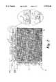
- FIG. 2is a schematic diagram illustrating the internal structure of a typical LCD panel
- FIGS. 3(a) to 3(c)are waveforms illustrating the memory cycles of the display driver and the host for different conditions, for an embodiment of LCD panel controller implementing a fixed interleave ratio.
- the LCD panel controller 10comprises a display driver 12 driving a display panel 14, a memory/interface block 16, a frame memory 18 and a host computer 20.
- the memory interface block 16implements an asynchronous transfer protocol for memory access and arbitration between requests for memory access by the display driver 12 and one or more other interfaces shown in the memory/interface block 16.
- the LCD panel 14has a line input buffer which stores a line of data before displaying it.
- the displaymay receive the data in a single block or several smaller blocks, provided the full line of data is in the buffer by the end of the line period, when it is clocked into the display electrodes by the line sync pulse.
- a conventional LCD display panel 14which typically comprises an LCD element 15 with row select logic and level drivers 17, a column line shift register 19 and column data latch and level drivers 21.
- the row drivers 17are simpler and step a select voltage level down the rows of the element 15, effectively selecting a single row at a time, on each line sync pulse.
- the column drivers 21hold the column drive data on the level drivers for a whole line period by latching the data once it has been shifted into the shift register 19 above. Once the data has been latched across by the line sync pulse, the next line of data can be shifted into the register.
- the display panel 14has an inherent line storage facility in the form of the shift register 19 and, within certain limits, the shift register can accept data for the next line to be displayed at any point within the preceding line period.
- the frame memory 18is augmented by an inking plane 18 1 to minimise the need to manipulate data.
- a page of text annotated with manuscript notes via the pen input devicerequires only the inking plane 18 1 to be modified to include the manuscript notes.
- the display driver 12comprises a control signal generator 24 which provides the correct clock and synchronisation signals to the display panel 14 and increments an address generator 26 after each transfer from memory.
- the control signal generator 24also initiates requests for data from the frame memory 18 via a memory arbiter 28, using an asynchronous request-acknowledge protocol as to be described below.
- datais transferred from the frame memory 18 via the memory arbiter 28 to a data mixer 30 which combines data from the frame memory 18 and the inking plane 18 1 , into a single data word corresponding to the output value of the particular pixel to be displayed.
- the output from the data mixer 30is passed to a greyscale generator 32 which generates a spatio-temporal dither where the LCD panel 14 does not have an inherent greyscale capability.
- the output from the greyscale generator 32is a binary data bit corresponding to the drive of each pixel. This is then supplied to the LCD panel 14 where it is stored temporarily in the column line shift register 19 until the line of data is complete and the control signal generator outputs a line sync pulse to cause the new line of pixels to be displayed.
- the memory/interface block 16also includes two further interfaces, namely a host interface 34 connected to the host computer 20, and a pen access 36.
- the host interface 34allows the host 20 to read or write from one to four pixels of data into the frame memory/inking plane 18,18 1 .
- the host interface 34maps an arbitrary (x,y) address to the physical memory address and also maps the data position within the sixty-four bit word.
- the pen access 36provides a single pixel write access to the inking plane 181 given a (x,y) pointer. Both the host interface 34 and the pen access 36 may initiate data requests from the memory arbiter 28 using an asynchronous request-acknowledge protocol.
- This particular examplestores data in the memory and operates on a "dual scan" basis, where data for two rows, separated by half the display screen, is clocked simultaneously into the upper and lower column drivers of the display panel 14. For ease of installation only one set of column drivers is shown in FIG. 2.
- the datais stored in the frame memory/inking plane 18, 18 1 , in an interleaved form.
- the database between the frame memory 18 and the memory arbiter 28is sixty-four bits wide with thirty-two bits for the upper screen and thirty-two bits for the lower screen at each address. Within each thirty-two bit word, data for four pixels is stored, with four bits for the frame memory 18 plane, and four bits for the inking plane 18 1 .
- the frame datais actually interleaved, the hardware address mapping described makes it appear as a continuous two-dimensional plane to the remaining interfaces.
- the memory arbiter 28provides an asynchronous bus control using a two-line four-phase asynchronous request-acknowledge protocol for the display driver 12, the host interface 34 and the pen access 36.
- the arbiter 28arbitrates and ensures that for each line period, the display driver has access to the memory for sufficient memory cycles to make up the line of data. This may be achieved in two ways, either by implementing a fixed interleave ratio between the display memory accesses and non-display memory accesses in response to competing requests. Alternatively this may be achieved by implementing a variable interleave ratio which may be modified through each line period in accordance with the proportion of the line of data sent to the display.
- the interleave ratiois selected taking into account the timing of the line period and the memory access cycles to ensure that, in the worst case, where there is a constant demand for memory access from the other memory users, the display driver 12 is allowed sufficient memory access cycles during each line period to make up a complete line of data for the display.
- the arbitermight typically provide 2:1 interleaving for display:non-display memory access cycles, but a different fixed ratio could apply for other combinations and displays and memory.
- the arbiter 28includes means which, during each line period, determines how much of each line of data to be set to the display has already been accessed and/or how much is still to come. The arbiter then modifies the interleave ratio which initially is set at a lower level than the fixed ratio referred to above. The proportion of the line of data is monitored and at stages through the line period, if it becomes apparent that there is still greater than a preset target proportion of the line left to access, the interleave ratio implemented by the arbiter is increased.
- the arbiter 28may initially apply a 1:1 ratio for display:non-display accesses at the beginning of each line period, and then increase this through the line period 2:1,3:1 etc., as the end of the line period approaches.
- FIG. 3(a)shows the display driver access and host access for a normal fixed interleave ratio mode for a period in which no host access is required.
- the data for the LCD panel 14is read as quickly as possible in consecutive memory accesses and fed in a burst into the panel shift register during the first portion of each line period, with the controller idling for the rest of the line period, thereby reducing quiescent current consumption.
- FIG. 3(b)shows the worst case, where the host requires continuous access to the memory in an arrangement with a fixed 2:1 interleaving ratio.
- the controllerprovides 2:1 interleaving for most of the line period with a short burst of continuous access for the host at the end of each line period, when the input buffer/shift register of the LCD panel is already full.
- the interleavingis driven by the competing memory requests and this ensures that the interleaving is applied only when required, thus providing a flexible and dynamic interleaving scheme.
- the arbiter 28allows substantially immediate access to any interface requesting access and this will continue until there is a competing request from another interface whereupon the arbiter will apply the relevant interleave ratio.
- the memory arbiterimplements a "priority burst access" mode in which it detects that the host requires only a small number of accesses (six in this example).
- the arbiterinterrupts the control signal generator 20 and allows the host immediate access.
- the arbitereffectively prioritises requests for data access by the host and grants immediate access, provided this will leave sufficient time for substantially all of the remainder of the display line to be accessed within the remainder of the line period.
Landscapes
- Engineering & Computer Science (AREA)
- Physics & Mathematics (AREA)
- Computer Hardware Design (AREA)
- General Physics & Mathematics (AREA)
- Theoretical Computer Science (AREA)
- Multimedia (AREA)
- Chemical & Material Sciences (AREA)
- Crystallography & Structural Chemistry (AREA)
- Liquid Crystal Display Device Control (AREA)
- Digital Computer Display Output (AREA)
- Control Of Indicators Other Than Cathode Ray Tubes (AREA)
Abstract
Description
This invention relates to display controllers for controlling displays which are capable of storing one or more lines of data, and to systems incorporating said controllers. In particular, but not exclusively, this invention relates to display controllers for controlling LCD panel displays.
Conventional LCD panel drivers have in the past been derived from controllers designed for cathode ray tubes (CRTs), which are designed to provide a constant pixel output and which thus require a uniform data transfer. Consequently these have been synchronous devices requiring permanent clocks and fast memory access. With more complex displays requiring higher bandwidth, an increasing proportion of the gate count becomes dedicated to generating the clock signals and maintaining stability of the clock signal throughout the circuit. This contributes significantly to the power consumption of the display system. Also, most CRT controllers and the LCD drivers derived therefrom are built with backwards compatibility so that the display can handle earlier graphics adapters, and this means that, whilst a significant proportion of the logic is not actually used in most applications, this still contributes to the gate count. The synchronous operation also places rigid constraints on the timing of memory access and may necessitate the use of fast and expensive memory such as VRAM if the host or other memory interfaces require rapid memory access, or if there are increased numbers of other interfaces, such as a pen interface, an image decompression unit, a video source, another host or another display. There exist computer graphics systems which attempt to provide greater flexibility and access by the host by providing a frame or half-frame buffer, often referred to as a "frame accelerator", which receives data from the device memory before it is sent to the display, and which acts as a buffer between host accesses and the display access. However, these systems require additional memory which increases their cost. EP-A-0228135 describes an arrangement for programmable sharing of display memory between a CRT display and one or more other resources. In this arrangement, the data transfer is essentially synchronous and, in certain modes, display process and update accesses to the memory may be interleaved under software control.
As portable computing appliances become more widespread, there is a growing need for low power consumption display controllers which can use a moderate speed memory whilst providing a good level of memory access to other memory users, and which can be manufactured relatively economically, without requiring significant amounts of additional memory.
We have realised that many non-CRT displays have an inherent line storage ability prior to display, (for example, a data register within the LCD column driver devices), and that this fact can be used to advantage because it allows re-synchronisation of data transfer to different clocks. For example in twisted nematic (TN) or supertwist nematic (STN) LCDs, the optical effect works on the RMS average of the voltages seen during a time frame. Serially accessed line registers build up a store of data during the previous line time, and non-uniformity in the data transfer is acceptable. Variation in the line synchronisation time manifests as optical differences in the LCD; most LCDs of this type can tolerate up to 5% variation in line synchronisation time with "one off" variations of typically 50-100%.
In active matrix LCDs (AMLCD) the liquid crystal is driven on the voltage applied. The line access time is relatively unimportant and thus non-uniformities both within the line and also between lines can be tolerated. A minimum line access time must be allowed, for the pixel drive voltage to stabilise, but the frame rate can be altered by typically 50-100% without significant optical interference.
In bistable technologies the voltage holding ratio of the material may be seen as infinite and so non-uniform data transfer can be tolerated.
The invention thus applies broadly to non-CRT displays which have an inherent or associated register or storage facility, including the technologies referred to above, as well as many others, such as "On Silicon" technologies, for example LC over silicon, digital micromirrors, poly-Si light valves, etc.
Thus, in such displays, an asynchronous arbitration and memory access protocol may allocate the memory access effectively between the display and other memory users. On this basis, we have developed a display controller for non-CRT displays which provides effective access to the memory by the display and one or more other users, and which may be implemented with low speed, low cost, volume memory. The controller may have a substantially reduced gate count compared to circuits derived from CRT displays, and a consequently reduced current consumption.
Accordingly, in one aspect, this invention provides a display controller for a display system comprising:
a memory means for storing data to be displayed,
a display means having associated therewith means capable of storing one or more lines or parts thereof of data to be displayed,
one or more other interface means requiring access to said memory means,
memory access control means for arbitrating between competing requests for memory access by said display means and one or more of the other interface means to interleave memory accesses by said display means and said one or more other interface means, and operable in use to effect non-uniform or asynchronous data transfer from said memory means to said display means.
By using non-uniform or asynchronous data transfer many of the constraints on timing imposed by synchronous operation are removed, allowing a flexible and optimised memory access by the display and other memory users, minimising the impact on the performance and design constraints of the display or the other memory interfaces.
As compared with EP-A-0228135, embodiments of a display controller in accordance with this invention allow interleaving to be driven by competing requests for memory access rather than by software control. This means that the controller is far more flexible and allows "dynamic" interleaving, that is interleaving only when required by the competing requests.
The non-uniform data transfer may be effected synchronously if the clock speed is high enough. The buffer means may form part of the display means or part of the controller.
The memory access control means preferably implements a prioritisation technique in which it determines the relative priority of requests for memory access, and arbitrates between said requests on the basis of said priority. In the event of competing requests for memory access, the memory access control means preferably provides interleaved access to said memory means by said display means and one or more other interface means throughout at least a substantial proportion of the line period of said display means. The interleave ratio may be fixed or variable. Thus where a variable interleave ratio is implemented, the ratio may be set by determining, during each line period, the proportion of the current line of data that has been accessed, and adjusting the interleave ratio in accordance with the proportion of the current line of data still to be accessed.
Whilst various forms of non-uniform or non-synchronous transfer may be employed, it is preferred for the memory access control means to use an asynchronous handshake in response to a request for memory access by said means or a request for memory access by said other interface means.
The invention also extends in other aspects to display systems incorporating the display controller described above, and to methods of controlling memory access and data transfer as implemented in the above apparatus.
Thus, in a further aspect, this invention provides a display system comprising:
a memory means for storing data to be displayed;
a display means capable of storing one or more lines or parts thereof of data to be displayed, and requiring access to said memory means;
one or more interface means also requiring access to said memory means, and
memory access control means for arbitrating between competing requests for memory access by said display means and said other interface means to interleave memory accesses by said display means and said one or more other interface means, and operable in use to effect non-uniform or asynchronous data transfer from said memory means to said display means.
Said display means preferably comprises a liquid crystal display. In a typical arrangement, said display means includes line or column drive means for applying to said display means line or column drive data, and further includes shift register means for storing said one or more lines or parts thereof prior to transfer to said line or column drive means.
In one arrangement, said memory access control means is operable to apply a fixed interleave ratio of accesses by said display means and said one or more interface means to said memory means in response to competing requests for memory access from said display means and said one or more interface means.
In another arrangement said memory access control means is operable to apply a variable interleave ratio of accesses by said display means and said one or more interface means to said memory means, which is dependent in a given line period on the proportion of the current line of data still to be transferred to said display means.
The memory access means may also be operable in a given line period to provide one or more of said other interface means with limited period priority access to said memory means, provided the resultant balance of the line period is sufficient to allow substantially the whole of the line of display data to be accessed within said line period.
Whilst the invention has been described above, it extends to any inventive combination of features set out above or in the following description.
The invention may be performed in various ways and, by way of example only, an embodiment thereof will now be described in detail, reference being made to the accompanying drawings in which:
FIG. 1 is a block diagram of an embodiment of an LCD panel controller in accordance with this invention;
FIG. 2 is a schematic diagram illustrating the internal structure of a typical LCD panel;
FIGS. 3(a) to 3(c) are waveforms illustrating the memory cycles of the display driver and the host for different conditions, for an embodiment of LCD panel controller implementing a fixed interleave ratio.
TheLCD panel controller 10 comprises adisplay driver 12 driving adisplay panel 14, a memory/interface block 16, aframe memory 18 and ahost computer 20. Thememory interface block 16 implements an asynchronous transfer protocol for memory access and arbitration between requests for memory access by thedisplay driver 12 and one or more other interfaces shown in the memory/interface block 16. In this example, theLCD panel 14 has a line input buffer which stores a line of data before displaying it. The display may receive the data in a single block or several smaller blocks, provided the full line of data is in the buffer by the end of the line period, when it is clocked into the display electrodes by the line sync pulse.
Referring to FIG. 2, a conventionalLCD display panel 14 which typically comprises anLCD element 15 with row select logic andlevel drivers 17, a columnline shift register 19 and column data latch andlevel drivers 21. Therow drivers 17 are simpler and step a select voltage level down the rows of theelement 15, effectively selecting a single row at a time, on each line sync pulse. Thecolumn drivers 21 hold the column drive data on the level drivers for a whole line period by latching the data once it has been shifted into theshift register 19 above. Once the data has been latched across by the line sync pulse, the next line of data can be shifted into the register. Thus thedisplay panel 14 has an inherent line storage facility in the form of theshift register 19 and, within certain limits, the shift register can accept data for the next line to be displayed at any point within the preceding line period.
In this example of LCD panel controller, which has apen input device 22, theframe memory 18 is augmented by an inkingplane 181 to minimise the need to manipulate data. In this way, a page of text annotated with manuscript notes via the pen input device requires only the inkingplane 181 to be modified to include the manuscript notes.
Thedisplay driver 12 comprises acontrol signal generator 24 which provides the correct clock and synchronisation signals to thedisplay panel 14 and increments anaddress generator 26 after each transfer from memory. Thecontrol signal generator 24 also initiates requests for data from theframe memory 18 via amemory arbiter 28, using an asynchronous request-acknowledge protocol as to be described below. In response to such requests, data is transferred from theframe memory 18 via thememory arbiter 28 to adata mixer 30 which combines data from theframe memory 18 and the inkingplane 181, into a single data word corresponding to the output value of the particular pixel to be displayed. The output from thedata mixer 30 is passed to agreyscale generator 32 which generates a spatio-temporal dither where theLCD panel 14 does not have an inherent greyscale capability. The output from thegreyscale generator 32 is a binary data bit corresponding to the drive of each pixel. This is then supplied to theLCD panel 14 where it is stored temporarily in the columnline shift register 19 until the line of data is complete and the control signal generator outputs a line sync pulse to cause the new line of pixels to be displayed. The memory/interface block 16 also includes two further interfaces, namely ahost interface 34 connected to thehost computer 20, and apen access 36. Thehost interface 34 allows thehost 20 to read or write from one to four pixels of data into the frame memory/inkingplane host interface 34 maps an arbitrary (x,y) address to the physical memory address and also maps the data position within the sixty-four bit word. Thepen access 36 provides a single pixel write access to the inkingplane 181 given a (x,y) pointer. Both thehost interface 34 and thepen access 36 may initiate data requests from thememory arbiter 28 using an asynchronous request-acknowledge protocol.
This particular example stores data in the memory and operates on a "dual scan" basis, where data for two rows, separated by half the display screen, is clocked simultaneously into the upper and lower column drivers of thedisplay panel 14. For ease of installation only one set of column drivers is shown in FIG. 2. The data is stored in the frame memory/inkingplane frame memory 18 and thememory arbiter 28 is sixty-four bits wide with thirty-two bits for the upper screen and thirty-two bits for the lower screen at each address. Within each thirty-two bit word, data for four pixels is stored, with four bits for theframe memory 18 plane, and four bits for the inkingplane 181. Although in this example the frame data is actually interleaved, the hardware address mapping described makes it appear as a continuous two-dimensional plane to the remaining interfaces.
In operation, thememory arbiter 28 provides an asynchronous bus control using a two-line four-phase asynchronous request-acknowledge protocol for thedisplay driver 12, thehost interface 34 and thepen access 36.
In the event of competing requests for memory access from two or more of thecontrol signal generator 24, thehost interface 34 and thepen access 36, thearbiter 28 arbitrates and ensures that for each line period, the display driver has access to the memory for sufficient memory cycles to make up the line of data. This may be achieved in two ways, either by implementing a fixed interleave ratio between the display memory accesses and non-display memory accesses in response to competing requests. Alternatively this may be achieved by implementing a variable interleave ratio which may be modified through each line period in accordance with the proportion of the line of data sent to the display.
In the first arrangement, the interleave ratio is selected taking into account the timing of the line period and the memory access cycles to ensure that, in the worst case, where there is a constant demand for memory access from the other memory users, thedisplay driver 12 is allowed sufficient memory access cycles during each line period to make up a complete line of data for the display. Thus, in this example the arbiter might typically provide 2:1 interleaving for display:non-display memory access cycles, but a different fixed ratio could apply for other combinations and displays and memory.
In the variable or adaptive implementation, thearbiter 28 includes means which, during each line period, determines how much of each line of data to be set to the display has already been accessed and/or how much is still to come. The arbiter then modifies the interleave ratio which initially is set at a lower level than the fixed ratio referred to above. The proportion of the line of data is monitored and at stages through the line period, if it becomes apparent that there is still greater than a preset target proportion of the line left to access, the interleave ratio implemented by the arbiter is increased. Thus, for example, thearbiter 28 may initially apply a 1:1 ratio for display:non-display accesses at the beginning of each line period, and then increase this through the line period 2:1,3:1 etc., as the end of the line period approaches.
FIG. 3(a) shows the display driver access and host access for a normal fixed interleave ratio mode for a period in which no host access is required. Here the data for theLCD panel 14 is read as quickly as possible in consecutive memory accesses and fed in a burst into the panel shift register during the first portion of each line period, with the controller idling for the rest of the line period, thereby reducing quiescent current consumption.
FIG. 3(b) shows the worst case, where the host requires continuous access to the memory in an arrangement with a fixed 2:1 interleaving ratio. Here the controller provides 2:1 interleaving for most of the line period with a short burst of continuous access for the host at the end of each line period, when the input buffer/shift register of the LCD panel is already full.
It will be appreciated that the interleaving is driven by the competing memory requests and this ensures that the interleaving is applied only when required, thus providing a flexible and dynamic interleaving scheme. When there are no longer any competing requests, thearbiter 28 allows substantially immediate access to any interface requesting access and this will continue until there is a competing request from another interface whereupon the arbiter will apply the relevant interleave ratio.
Finally, in FIG. 3(c) the memory arbiter implements a "priority burst access" mode in which it detects that the host requires only a small number of accesses (six in this example). The arbiter interrupts thecontrol signal generator 20 and allows the host immediate access. We have found that, even though this may mean that the complete line of display driver accesses take longer than the nominal line period, and thus disturb the line to line timing, no effect is seen, even with aberrations of up to +/- 20%, provided that the extended accesses are limited and occur randomly. In this last mode, the arbiter effectively prioritises requests for data access by the host and grants immediate access, provided this will leave sufficient time for substantially all of the remainder of the display line to be accessed within the remainder of the line period.
Claims (12)
1. A display controller for a display system comprising:
a memory means for storing data to be displayed,
a display means having associated therewith means for storing one or more lines or parts thereof of data to be displayed,
one or more other interface means requiring access to said memory means,
memory access control means for arbitrating between competing requests for memory access by said display means and one or more of the other interface means to interleave memory accesses by said display means and said one or more other interface means, and operable in use to effect non-uniform or asynchronous data transfer from said memory means to said display means.
2. A display controller according to claim 1, wherein said memory access control means determines the relative priority of requests for memory access, and arbitrates between said requests on the basis of said priority.
3. A display controller according to claim 1, wherein said memory access control means is operable to provide a fixed interleave ratio between accesses by said display means and accesses by said one or more interface means, in response to competing requests for memory access by said display means and said one or more other interface means.
4. A display controller according to claim 1, wherein said memory access control means is operable to provide a variable interleave ratio between accesses by said display means and accesses by said one or more interface means, in response to competing requests for memory access by said display means and said one or more other interface means.
5. A display controller according to claim 4, wherein said memory access control means includes means for determining, during each line period, a proportion of a current line of data that has been accessed for transfer to said display means, and means for adjusting an interleave ratio in accordance with the proportion of said current line of data still to be accessed.
6. A display controller according to claim 1, wherein said memory access control means uses an asynchronous handshake in response to a request for memory access by said display means or a request for memory access by said other interface means.
7. A display system comprising:
a memory means for storing data to be displayed;
a display means for storing one or more lines or parts thereof of data to be displayed, and requiring access to said memory means;
one or more interface means also requiring access to said memory means, and
memory access control means for arbitrating between competing requests for memory access by said display means and said other interface means to interleave memory accesses by said display means and said one or more other interface means, and operable in use to effect non-uniform or asynchronous data transfer from said memory means to said display means.
8. A display system according to claim 7, wherein said display means comprises a liquid crystal display.
9. A display system according to claim 7, wherein said display means includes line or column drive means for applying to said display means line or column drive data, and further includes shift register means for storing said one or more lines or parts thereof prior to transfer to said line or column drive means.
10. A display system according to claim 7, wherein said memory access control means is operable to apply a fixed interleave ratio of accesses by said display means and said one or more interface means to said memory means in response to competing requests for memory access from said display means and said one or more interface means.
11. A display system according to claim 7, wherein said memory access control means is operable to apply a variable interleave ratio of accesses by said display means and said one or more interface means to said memory means which is dependent in a given line period on the proportion of the current line of data still to be transferred to said display means.
12. A display system according to claim 7, wherein said memory access means is also operable in a given line period to provide one or more of said other interface means with limited period priority access to said memory means, provided a resultant balance of the line period is sufficient to allow substantially a whole of a line of display data to be accessed within said line period.
Priority Applications (3)
| Application Number | Priority Date | Filing Date | Title |
|---|---|---|---|
| EP96300452AEP0786756B1 (en) | 1996-01-23 | 1996-01-23 | Data transfer arbitration for display controller |
| US08/782,847US5959640A (en) | 1996-01-23 | 1997-01-13 | Display controllers |
| JP00840997AJP3926417B2 (en) | 1996-01-23 | 1997-01-21 | Display control device |
Applications Claiming Priority (2)
| Application Number | Priority Date | Filing Date | Title |
|---|---|---|---|
| EP96300452AEP0786756B1 (en) | 1996-01-23 | 1996-01-23 | Data transfer arbitration for display controller |
| US08/782,847US5959640A (en) | 1996-01-23 | 1997-01-13 | Display controllers |
Publications (1)
| Publication Number | Publication Date |
|---|---|
| US5959640Atrue US5959640A (en) | 1999-09-28 |
Family
ID=26143538
Family Applications (1)
| Application Number | Title | Priority Date | Filing Date |
|---|---|---|---|
| US08/782,847Expired - LifetimeUS5959640A (en) | 1996-01-23 | 1997-01-13 | Display controllers |
Country Status (3)
| Country | Link |
|---|---|
| US (1) | US5959640A (en) |
| EP (1) | EP0786756B1 (en) |
| JP (1) | JP3926417B2 (en) |
Cited By (27)
| Publication number | Priority date | Publication date | Assignee | Title |
|---|---|---|---|---|
| US6618048B1 (en) | 1999-10-28 | 2003-09-09 | Nintendo Co., Ltd. | 3D graphics rendering system for performing Z value clamping in near-Z range to maximize scene resolution of visually important Z components |
| US6636214B1 (en) | 2000-08-23 | 2003-10-21 | Nintendo Co., Ltd. | Method and apparatus for dynamically reconfiguring the order of hidden surface processing based on rendering mode |
| US20040027356A1 (en)* | 2002-08-08 | 2004-02-12 | Satoshi Takamura | Liquid crystal display control device |
| US6700586B1 (en) | 2000-08-23 | 2004-03-02 | Nintendo Co., Ltd. | Low cost graphics with stitching processing hardware support for skeletal animation |
| US6707458B1 (en) | 2000-08-23 | 2004-03-16 | Nintendo Co., Ltd. | Method and apparatus for texture tiling in a graphics system |
| US6717577B1 (en) | 1999-10-28 | 2004-04-06 | Nintendo Co., Ltd. | Vertex cache for 3D computer graphics |
| US20040160384A1 (en)* | 2003-02-18 | 2004-08-19 | Eric Jeffrey | Hardware method for arranging dual-STN display data in a single memory bank to eliminate a half frame buffer |
| US6811489B1 (en) | 2000-08-23 | 2004-11-02 | Nintendo Co., Ltd. | Controller interface for a graphics system |
| US6867781B1 (en) | 2000-08-23 | 2005-03-15 | Nintendo Co., Ltd. | Graphics pipeline token synchronization |
| US6940516B1 (en)* | 2000-09-28 | 2005-09-06 | Rockwell Automation Technologies, Inc. | Method and apparatus for video underflow detection in a raster engine |
| US20050239401A1 (en)* | 2004-03-30 | 2005-10-27 | Nicholas Nam | Multi-video interface for a mobile device |
| US7002591B1 (en) | 2000-08-23 | 2006-02-21 | Nintendo Co., Ltd. | Method and apparatus for interleaved processing of direct and indirect texture coordinates in a graphics system |
| US7023413B1 (en)* | 1997-10-24 | 2006-04-04 | Canon Kabushiki Kaisha | Memory controller and liquid crystal display apparatus using the same |
| US7034828B1 (en) | 2000-08-23 | 2006-04-25 | Nintendo Co., Ltd. | Recirculating shade tree blender for a graphics system |
| US7061502B1 (en) | 2000-08-23 | 2006-06-13 | Nintendo Co., Ltd. | Method and apparatus for providing logical combination of N alpha operations within a graphics system |
| US7075545B2 (en) | 2000-08-23 | 2006-07-11 | Nintendo Co., Ltd. | Graphics system with embedded frame buffer having reconfigurable pixel formats |
| US7100118B1 (en)* | 1999-03-05 | 2006-08-29 | Amulet Technologies, Llc | Graphical user interface engine for embedded systems |
| US7119813B1 (en) | 2000-06-02 | 2006-10-10 | Nintendo Co., Ltd. | Variable bit field encoding |
| US7184059B1 (en) | 2000-08-23 | 2007-02-27 | Nintendo Co., Ltd. | Graphics system with copy out conversions between embedded frame buffer and main memory |
| US7196710B1 (en) | 2000-08-23 | 2007-03-27 | Nintendo Co., Ltd. | Method and apparatus for buffering graphics data in a graphics system |
| US7205999B2 (en) | 2000-08-23 | 2007-04-17 | Nintendo Co., Ltd. | Method and apparatus for environment-mapped bump-mapping in a graphics system |
| US7215339B1 (en) | 2000-09-28 | 2007-05-08 | Rockwell Automation Technologies, Inc. | Method and apparatus for video underflow detection in a raster engine |
| US7307640B2 (en) | 2000-08-23 | 2007-12-11 | Nintendo Co., Ltd. | Method and apparatus for efficient generation of texture coordinate displacements for implementing emboss-style bump mapping in a graphics rendering system |
| CN100399412C (en)* | 2005-05-24 | 2008-07-02 | 乐金电子(昆山)电脑有限公司 | LCD module interface device and method |
| US7538772B1 (en) | 2000-08-23 | 2009-05-26 | Nintendo Co., Ltd. | Graphics processing system with enhanced memory controller |
| US7576748B2 (en) | 2000-11-28 | 2009-08-18 | Nintendo Co. Ltd. | Graphics system with embedded frame butter having reconfigurable pixel formats |
| US9256531B2 (en) | 2012-06-19 | 2016-02-09 | Samsung Electronics Co., Ltd. | Memory system and SoC including linear addresss remapping logic |
Citations (11)
| Publication number | Priority date | Publication date | Assignee | Title |
|---|---|---|---|---|
| US4511965A (en)* | 1983-03-21 | 1985-04-16 | Zenith Electronics Corporation | Video ram accessing system |
| EP0182454A2 (en)* | 1984-07-23 | 1986-05-28 | Texas Instruments Incorporated | Video system controller with a row address override circuit |
| EP0228135A2 (en)* | 1985-12-30 | 1987-07-08 | Koninklijke Philips Electronics N.V. | Programmable sharing of display memory between update and display processes in a raster scan video controller |
| US4815033A (en)* | 1985-12-10 | 1989-03-21 | Advanced Micro Devices, Inc. | Method and apparatus for accessing a color palette synchronously during refreshing of a monitor and asynchronously during updating of the palette |
| US4858107A (en)* | 1985-03-11 | 1989-08-15 | General Electric Company | Computer device display system using conditionally asynchronous memory accessing by video display controller |
| US5001652A (en)* | 1987-03-20 | 1991-03-19 | International Business Machines Corporation | Memory arbitration for video subsystems |
| FR2677158A1 (en)* | 1991-05-27 | 1992-12-04 | Guth Claude | Column control circuit for a matrix screen |
| EP0546780A1 (en)* | 1991-12-10 | 1993-06-16 | Xerox Corporation | AM TFT LCD universal controller |
| US5335322A (en)* | 1992-03-31 | 1994-08-02 | Vlsi Technology, Inc. | Computer display system using system memory in place or dedicated display memory and method therefor |
| US5450542A (en)* | 1993-11-30 | 1995-09-12 | Vlsi Technology, Inc. | Bus interface with graphics and system paths for an integrated memory system |
| US5563623A (en)* | 1994-11-23 | 1996-10-08 | Motorola, Inc. | Method and apparatus for driving an active addressed display |
- 1996
- 1996-01-23EPEP96300452Apatent/EP0786756B1/ennot_activeExpired - Lifetime
- 1997
- 1997-01-13USUS08/782,847patent/US5959640A/ennot_activeExpired - Lifetime
- 1997-01-21JPJP00840997Apatent/JP3926417B2/ennot_activeExpired - Fee Related
Patent Citations (11)
| Publication number | Priority date | Publication date | Assignee | Title |
|---|---|---|---|---|
| US4511965A (en)* | 1983-03-21 | 1985-04-16 | Zenith Electronics Corporation | Video ram accessing system |
| EP0182454A2 (en)* | 1984-07-23 | 1986-05-28 | Texas Instruments Incorporated | Video system controller with a row address override circuit |
| US4858107A (en)* | 1985-03-11 | 1989-08-15 | General Electric Company | Computer device display system using conditionally asynchronous memory accessing by video display controller |
| US4815033A (en)* | 1985-12-10 | 1989-03-21 | Advanced Micro Devices, Inc. | Method and apparatus for accessing a color palette synchronously during refreshing of a monitor and asynchronously during updating of the palette |
| EP0228135A2 (en)* | 1985-12-30 | 1987-07-08 | Koninklijke Philips Electronics N.V. | Programmable sharing of display memory between update and display processes in a raster scan video controller |
| US5001652A (en)* | 1987-03-20 | 1991-03-19 | International Business Machines Corporation | Memory arbitration for video subsystems |
| FR2677158A1 (en)* | 1991-05-27 | 1992-12-04 | Guth Claude | Column control circuit for a matrix screen |
| EP0546780A1 (en)* | 1991-12-10 | 1993-06-16 | Xerox Corporation | AM TFT LCD universal controller |
| US5335322A (en)* | 1992-03-31 | 1994-08-02 | Vlsi Technology, Inc. | Computer display system using system memory in place or dedicated display memory and method therefor |
| US5450542A (en)* | 1993-11-30 | 1995-09-12 | Vlsi Technology, Inc. | Bus interface with graphics and system paths for an integrated memory system |
| US5563623A (en)* | 1994-11-23 | 1996-10-08 | Motorola, Inc. | Method and apparatus for driving an active addressed display |
Non-Patent Citations (1)
| Title |
|---|
| European Search Report, Application No. EP 96 30 0452, dated Jul. 9, 1996 by Examiner L. Farricella, 2 pages.* |
Cited By (42)
| Publication number | Priority date | Publication date | Assignee | Title |
|---|---|---|---|---|
| US7023413B1 (en)* | 1997-10-24 | 2006-04-04 | Canon Kabushiki Kaisha | Memory controller and liquid crystal display apparatus using the same |
| US20070106928A1 (en)* | 1999-03-05 | 2007-05-10 | Amulet Technologies, Llc | Graphical user interface engine for embedded systems |
| US7100118B1 (en)* | 1999-03-05 | 2006-08-29 | Amulet Technologies, Llc | Graphical user interface engine for embedded systems |
| US6618048B1 (en) | 1999-10-28 | 2003-09-09 | Nintendo Co., Ltd. | 3D graphics rendering system for performing Z value clamping in near-Z range to maximize scene resolution of visually important Z components |
| US6717577B1 (en) | 1999-10-28 | 2004-04-06 | Nintendo Co., Ltd. | Vertex cache for 3D computer graphics |
| US7119813B1 (en) | 2000-06-02 | 2006-10-10 | Nintendo Co., Ltd. | Variable bit field encoding |
| US7538772B1 (en) | 2000-08-23 | 2009-05-26 | Nintendo Co., Ltd. | Graphics processing system with enhanced memory controller |
| US6707458B1 (en) | 2000-08-23 | 2004-03-16 | Nintendo Co., Ltd. | Method and apparatus for texture tiling in a graphics system |
| US6867781B1 (en) | 2000-08-23 | 2005-03-15 | Nintendo Co., Ltd. | Graphics pipeline token synchronization |
| US7317459B2 (en) | 2000-08-23 | 2008-01-08 | Nintendo Co., Ltd. | Graphics system with copy out conversions between embedded frame buffer and main memory for producing a streaming video image as a texture on a displayed object image |
| US8098255B2 (en) | 2000-08-23 | 2012-01-17 | Nintendo Co., Ltd. | Graphics processing system with enhanced memory controller |
| US7002591B1 (en) | 2000-08-23 | 2006-02-21 | Nintendo Co., Ltd. | Method and apparatus for interleaved processing of direct and indirect texture coordinates in a graphics system |
| US7995069B2 (en) | 2000-08-23 | 2011-08-09 | Nintendo Co., Ltd. | Graphics system with embedded frame buffer having reconfigurable pixel formats |
| US7034828B1 (en) | 2000-08-23 | 2006-04-25 | Nintendo Co., Ltd. | Recirculating shade tree blender for a graphics system |
| US7061502B1 (en) | 2000-08-23 | 2006-06-13 | Nintendo Co., Ltd. | Method and apparatus for providing logical combination of N alpha operations within a graphics system |
| US7701461B2 (en) | 2000-08-23 | 2010-04-20 | Nintendo Co., Ltd. | Method and apparatus for buffering graphics data in a graphics system |
| US7075545B2 (en) | 2000-08-23 | 2006-07-11 | Nintendo Co., Ltd. | Graphics system with embedded frame buffer having reconfigurable pixel formats |
| US6636214B1 (en) | 2000-08-23 | 2003-10-21 | Nintendo Co., Ltd. | Method and apparatus for dynamically reconfiguring the order of hidden surface processing based on rendering mode |
| US6700586B1 (en) | 2000-08-23 | 2004-03-02 | Nintendo Co., Ltd. | Low cost graphics with stitching processing hardware support for skeletal animation |
| US7176919B2 (en) | 2000-08-23 | 2007-02-13 | Nintendo Co., Ltd. | Recirculating shade tree blender for a graphics system |
| US7184059B1 (en) | 2000-08-23 | 2007-02-27 | Nintendo Co., Ltd. | Graphics system with copy out conversions between embedded frame buffer and main memory |
| US7196710B1 (en) | 2000-08-23 | 2007-03-27 | Nintendo Co., Ltd. | Method and apparatus for buffering graphics data in a graphics system |
| US7205999B2 (en) | 2000-08-23 | 2007-04-17 | Nintendo Co., Ltd. | Method and apparatus for environment-mapped bump-mapping in a graphics system |
| US7307640B2 (en) | 2000-08-23 | 2007-12-11 | Nintendo Co., Ltd. | Method and apparatus for efficient generation of texture coordinate displacements for implementing emboss-style bump mapping in a graphics rendering system |
| US6811489B1 (en) | 2000-08-23 | 2004-11-02 | Nintendo Co., Ltd. | Controller interface for a graphics system |
| US7307638B2 (en) | 2000-08-23 | 2007-12-11 | Nintendo Co., Ltd. | Method and apparatus for interleaved processing of direct and indirect texture coordinates in a graphics system |
| US7215339B1 (en) | 2000-09-28 | 2007-05-08 | Rockwell Automation Technologies, Inc. | Method and apparatus for video underflow detection in a raster engine |
| US6940516B1 (en)* | 2000-09-28 | 2005-09-06 | Rockwell Automation Technologies, Inc. | Method and apparatus for video underflow detection in a raster engine |
| US7576748B2 (en) | 2000-11-28 | 2009-08-18 | Nintendo Co. Ltd. | Graphics system with embedded frame butter having reconfigurable pixel formats |
| US20040027356A1 (en)* | 2002-08-08 | 2004-02-12 | Satoshi Takamura | Liquid crystal display control device |
| US7064764B2 (en) | 2002-08-08 | 2006-06-20 | Oki Electric Industry Co., Ltd. | Liquid crystal display control device |
| US20040160384A1 (en)* | 2003-02-18 | 2004-08-19 | Eric Jeffrey | Hardware method for arranging dual-STN display data in a single memory bank to eliminate a half frame buffer |
| US7480484B2 (en) | 2004-03-30 | 2009-01-20 | Omnivision Technologies, Inc | Multi-video interface for a mobile device |
| US20050239401A1 (en)* | 2004-03-30 | 2005-10-27 | Nicholas Nam | Multi-video interface for a mobile device |
| CN100399412C (en)* | 2005-05-24 | 2008-07-02 | 乐金电子(昆山)电脑有限公司 | LCD module interface device and method |
| US9256531B2 (en) | 2012-06-19 | 2016-02-09 | Samsung Electronics Co., Ltd. | Memory system and SoC including linear addresss remapping logic |
| US10817199B2 (en) | 2012-06-19 | 2020-10-27 | Samsung Electronics Co., Ltd. | Memory system and SoC including linear address remapping logic |
| US11169722B2 (en) | 2012-06-19 | 2021-11-09 | Samsung Electronics Co., Ltd. | Memory system and SoC including linear address remapping logic |
| US11573716B2 (en) | 2012-06-19 | 2023-02-07 | Samsung Electronics Co., Ltd. | Memory system and SoC including linear address remapping logic |
| US11681449B2 (en) | 2012-06-19 | 2023-06-20 | Samsung Electronics Co., Ltd. | Memory system and SoC including linear address remapping logic |
| US11704031B2 (en) | 2012-06-19 | 2023-07-18 | Samsung Electronics Co., Ltd. | Memory system and SOC including linear address remapping logic |
| US12001698B2 (en) | 2012-06-19 | 2024-06-04 | Samsung Electronics Co., Ltd. | Memory system and SoC including linear address remapping logic |
Also Published As
| Publication number | Publication date |
|---|---|
| EP0786756A1 (en) | 1997-07-30 |
| JP3926417B2 (en) | 2007-06-06 |
| JPH09305373A (en) | 1997-11-28 |
| EP0786756B1 (en) | 2009-03-25 |
Similar Documents
| Publication | Publication Date | Title |
|---|---|---|
| US5959640A (en) | Display controllers | |
| JP2868650B2 (en) | Display device | |
| US7633474B2 (en) | Liquid crystal display and driving method thereof | |
| US6067071A (en) | Method and apparatus for expanding graphics images for LCD panels | |
| US5488385A (en) | Multiple concurrent display system | |
| US5874928A (en) | Method and apparatus for driving a plurality of displays simultaneously | |
| US6181312B1 (en) | Drive circuit for an active matrix liquid crystal display device | |
| KR920000355B1 (en) | Color display device | |
| US8223138B2 (en) | Partial frame memory FPR display device and writing and reading method thereof | |
| JPH11352938A (en) | Liquid crystal display device, driving method thereof, and scanning line driving circuit | |
| JP3126360B2 (en) | Display system and display control method thereof | |
| US6329975B1 (en) | Liquid-crystal display device with improved interface control | |
| US5754170A (en) | Transparent blocking of CRT refresh fetches during video overlay using dummy fetches | |
| JPH10133172A (en) | Drive circuit for simple matrix display device | |
| EP0918278B1 (en) | Circuit for simultaneous driving of liquid crystal display panel and television | |
| US6078316A (en) | Display memory cache | |
| KR100796748B1 (en) | Liquid crystal display and its driving device | |
| US5606336A (en) | Display control apparatus | |
| US5905483A (en) | Display control apparatus | |
| KR100472478B1 (en) | Method and apparatus for controlling memory access | |
| US8026921B2 (en) | Driving method, driving circuit and driving apparatus for a display system | |
| KR20040038411A (en) | Liquid crystal display and method of driving the same | |
| KR100495814B1 (en) | Thin Film Transistor Liquid Crystal Display Driving System | |
| JPH07129126A (en) | Image display device | |
| JPH06324650A (en) | Display driving device |
Legal Events
| Date | Code | Title | Description |
|---|---|---|---|
| AS | Assignment | Owner name:HEWLETT-PACKARD COMPANY, CALIFORNIA Free format text:ASSIGNMENT OF ASSIGNORS INTEREST;ASSIGNOR:HEWLETT-PACKARD LIMITED;REEL/FRAME:008418/0287 Effective date:19970218 | |
| STCF | Information on status: patent grant | Free format text:PATENTED CASE | |
| AS | Assignment | Owner name:HEWLETT-PACKARD COMPANY, COLORADO Free format text:MERGER;ASSIGNOR:HEWLETT-PACKARD COMPANY;REEL/FRAME:011523/0469 Effective date:19980520 | |
| FEPP | Fee payment procedure | Free format text:PAYOR NUMBER ASSIGNED (ORIGINAL EVENT CODE: ASPN); ENTITY STATUS OF PATENT OWNER: LARGE ENTITY | |
| FPAY | Fee payment | Year of fee payment:4 | |
| FPAY | Fee payment | Year of fee payment:8 | |
| FPAY | Fee payment | Year of fee payment:12 | |
| AS | Assignment | Owner name:HEWLETT-PACKARD DEVELOPMENT COMPANY, L.P., TEXAS Free format text:ASSIGNMENT OF ASSIGNORS INTEREST;ASSIGNOR:HEWLETT-PACKARD COMPANY;REEL/FRAME:026945/0699 Effective date:20030131 |