US5959444A - MOS transistor circuit and method for biasing a voltage generator - Google Patents
MOS transistor circuit and method for biasing a voltage generatorDownload PDFInfo
- Publication number
- US5959444A US5959444AUS08/989,698US98969897AUS5959444AUS 5959444 AUS5959444 AUS 5959444AUS 98969897 AUS98969897 AUS 98969897AUS 5959444 AUS5959444 AUS 5959444A
- Authority
- US
- United States
- Prior art keywords
- bias
- voltage
- node
- coupled
- transistor
- Prior art date
- Legal status (The legal status is an assumption and is not a legal conclusion. Google has not performed a legal analysis and makes no representation as to the accuracy of the status listed.)
- Expired - Lifetime
Links
Images

Classifications
- G—PHYSICS
- G05—CONTROLLING; REGULATING
- G05F—SYSTEMS FOR REGULATING ELECTRIC OR MAGNETIC VARIABLES
- G05F3/00—Non-retroactive systems for regulating electric variables by using an uncontrolled element, or an uncontrolled combination of elements, such element or such combination having self-regulating properties
- G05F3/02—Regulating voltage or current
- G05F3/08—Regulating voltage or current wherein the variable is DC
- G05F3/10—Regulating voltage or current wherein the variable is DC using uncontrolled devices with non-linear characteristics
- G05F3/16—Regulating voltage or current wherein the variable is DC using uncontrolled devices with non-linear characteristics being semiconductor devices
- G05F3/20—Regulating voltage or current wherein the variable is DC using uncontrolled devices with non-linear characteristics being semiconductor devices using diode- transistor combinations
- G05F3/205—Substrate bias-voltage generators
- G—PHYSICS
- G05—CONTROLLING; REGULATING
- G05F—SYSTEMS FOR REGULATING ELECTRIC OR MAGNETIC VARIABLES
- G05F3/00—Non-retroactive systems for regulating electric variables by using an uncontrolled element, or an uncontrolled combination of elements, such element or such combination having self-regulating properties
- G05F3/02—Regulating voltage or current
- G05F3/08—Regulating voltage or current wherein the variable is DC
- G05F3/10—Regulating voltage or current wherein the variable is DC using uncontrolled devices with non-linear characteristics
- G05F3/16—Regulating voltage or current wherein the variable is DC using uncontrolled devices with non-linear characteristics being semiconductor devices
- G05F3/20—Regulating voltage or current wherein the variable is DC using uncontrolled devices with non-linear characteristics being semiconductor devices using diode- transistor combinations
- G05F3/24—Regulating voltage or current wherein the variable is DC using uncontrolled devices with non-linear characteristics being semiconductor devices using diode- transistor combinations wherein the transistors are of the field-effect type only
- G05F3/242—Regulating voltage or current wherein the variable is DC using uncontrolled devices with non-linear characteristics being semiconductor devices using diode- transistor combinations wherein the transistors are of the field-effect type only with compensation for device parameters, e.g. channel width modulation, threshold voltage, processing, or external variations, e.g. temperature, loading, supply voltage
- G05F3/247—Regulating voltage or current wherein the variable is DC using uncontrolled devices with non-linear characteristics being semiconductor devices using diode- transistor combinations wherein the transistors are of the field-effect type only with compensation for device parameters, e.g. channel width modulation, threshold voltage, processing, or external variations, e.g. temperature, loading, supply voltage producing a voltage or current as a predetermined function of the supply voltage
Definitions
- the present inventionrelates generally to voltage generator circuits, and more specifically to a low power voltage generator circuit which utilizes the body effect of tracking transistors to ensure complementary drive transistors are never simultaneously turned ON.
- FIG. 1is a schematic of a conventional bias and equilibration voltage generator circuit 10 utilized in a conventional DRAM to generate the bias and equilibration voltage V CC /2.
- the voltage generator circuit 10includes a PMOS feedback transistor 12 which presents a variable resistance between a supply voltage V CC and a first bias node 14 in response to an output voltage on an output node 26 applied to its gate.
- the voltage generator circuit 10further includes a bias circuit 15 comprising an NMOS diode-coupled transistor 16 coupled between the first bias node 14 and a tracking node 17, and a PMOS diode-coupled transistor 18 coupled between the tracking node 17 and a second bias node 20.
- each diode-coupled transistor 16 and 18has its gate coupled to its drain and exhibits a current-voltage relationship that approximates a diode having a threshold voltage equal to the threshold voltage of the transistor.
- the threshold voltages of the diode-coupled transistors 16 and 18are designated as V tn1 and V tp1 , respectively.
- the diode-coupled transistors 16 and 18maintain a voltage differential between the first and second bias nodes 14 and 20 of approximately V tn1 +V tp1 .
- the diode-coupled transistor 18has its back-bias terminal coupled to its source in order to minimize its threshold voltage V tp1 , as will be explained in more detail below.
- An NMOS feedback transistor 22presents a variable resistance between the second bias node 20 and ground, or another suitable reference voltage, in response to the voltage on the output node 26 applied to its gate.
- the voltage generator circuit 10further includes an NMOS drive transistor 24 presenting a variable resistance between the supply voltage V CC and the output node 26 in response to the voltage on the first bias node 14 applied to its gate, and a PMOS drive transistor 28 presenting a variable resistance between the output node 26 and ground in response to the voltage on the second bias node 20 applied to its gate.
- the driver transistors 24 and 28are typically formed having larger current driving capacities than the transistors 12. 16. 18, and 22 to provide sufficient current for driving loads coupled to the output node 26.
- large current driving capacityenables the transistors 24 and 28 to quickly return the voltage on the output node 26 to the desired output voltage in response to load variations.
- the larger current driving capacity of the transistors 24 and 28may be achieved for example by increasing the respective channel widths of the transistors.
- the transistors 16, 18, 24, and 28have threshold voltages V tn1 , V tp1 , V tn2 , and V tp2 , as shown in FIG. 1. These threshold voltages determine the value of the output voltage developed by the generator circuit 10 on output node 26. In the bias and equilibration circuit 10, the desired output voltage on the node 26 is V CC /2, and the respective threshold voltages are selected accordingly. In addition, the threshold voltages ideally have values which ensure the NMOS drive transistor 24 and PMOS drive transistor 28 do not simultaneously present relatively low resistances between their respective sources and drains.
- the diode-coupled transistors 16 and 18 and driver transistors 24 and 28are formed such that the summation of the threshold voltages of the diode-coupled transistors 16 and 18 is less than the summation of the threshold voltages of the drive transistors 24 and 28: V tn1 +V tp1 ⁇ V tn2 +V tp2 .
- V tn1 +V tp1 ⁇ V tn2 +V tp2One skilled in the art will realize a finite current may flow through the drive transistors 24 and 28 even when the threshold voltages satisfy the desired relationship, but when the threshold voltages are so selected the power dissipated due to such finite current is typically negligible.
- the feedback transistor 12drives the voltage on the first bias node 14 toward the supply voltage V CC in response to the decreasing voltage on node 26.
- the NMOS drive transistor 24drives the voltage on the output node 26 toward the supply voltage V CC .
- the feedback transistor 12drives the voltage on the first bias node 14 back to the bias voltage until the quiescent operating condition is once again established.
- the feedback transistor 22 and drive transistor 28operate similar to transistors 12 and 24 to restore the desired output voltage.
- the feedback transistor 22drives the voltage on the second bias node 20 toward ground in response to the increasing voltage on node 26.
- the PMOS drive transistor 28drives the voltage on the output node 26 toward ground.
- the feedback transistor 22drives the voltage on the second bias node 20 back to the bias voltage until the quiescent operating condition is again established.
- the diode-coupled transistors 16 and 18be formed having respective threshold voltages satisfying the relationship V tn1 +V tp1 ⁇ V tn2 +V tp2 , which may be difficult to do.
- the threshold voltages of the diode-coupled transistors 16 and 18may be reduced in a variety of ways, including varying the channel width of the transistors, and varying the doping concentration in various regions of the transistors. Reducing the threshold voltages of the diode-coupled transistors 16 and 18 through either of these methods, however, may result in undesirable additional process steps when forming the voltage generator circuit 10.
- Another method of reducing the threshold voltage of a MOS transistoris utilizing the "body effect" of the transistor by coupling the back-bias voltage terminal of the transistor to its source.
- the body effect of a MOS transistoris the variation in the threshold voltage of the transistor as a function of the voltage across the source-substrate junction of the transistor.
- the threshold voltage of a MOS transistorincreases as the source-substrate voltage increases, and decreases as the source-substrate voltage decreases.
- the body effect of the transistor 18is utilized to lower its threshold voltage V tp1 by coupling its back-bias terminal to its source such that the source-substrate voltage of the transistor is approximately zero.
- the back-bias voltage terminal of both the diode-coupled transistors 16 and 18may not be simultaneously coupled to their respective sources because the threshold voltages of other transistors formed in the semiconductor substrate containing the voltage generator circuit 10 may be undesirably affected.
- one of the diode-coupled transistors 16 and 18is formed in a well region, and it is this transistor whose back-bias voltage terminal is coupled to its source. In the embodiment of FIG.
- the voltage generator circuit 10is formed in a p-type semiconductor substrate with the diode-coupled transistor 16 formed in the substrate and the diode-coupled transistor 18 formed in an n-well region.
- the back-bias voltage terminal of the transistor 18is coupled to its source while the back-bias voltage terminal of the transistor 16 is typically coupled to a negative voltage source, such as a -1.2 volt substrate pump circuit, or to ground.
- the transistor 18has the threshold voltage V tp1 , corresponding to a zero source-substrate voltage
- the transistor 16has the threshold voltage V tn1 corresponding to the voltage on the node 17 (approximately V CC /2 under quiescent operating conditions).
- the voltage on the node 17increases the threshold voltage V tn1 , relative to the value for zero source-substrate voltage, which makes it more difficult to ensure V tn1 +V tp1 is less than V tn2 +V tp2 as desired.
- a voltage generator circuitincludes a first drive MOS transistor having a first signal terminal adapted to receive a supply voltage, a gate terminal coupled to a first bias node, and a second signal terminal coupled to an output node.
- a second drive MOS transistorhas a first signal terminal coupled to the output node, a second signal terminal adapted to receive a reference voltage, and a gate terminal coupled to a second bias node.
- a feedback circuitis coupled to the output node, and is adapted to receive the supply and reference voltages. The feedback circuit develops first and second bias voltages on the first and second bias nodes, respectively, in response to a signal on the output node.
- a bias circuitincludes a first diode-coupled MOS bias transistor of a first conductivity type having its source coupled to the first bias node and drain coupled to a tracking node.
- a second diode-coupled MOS bias transistor of a second conductivity typehas its source coupled to the second bias node and drain coupled to the tracking node.
- One of the first and second MOS bias transistorsis formed in a well region in semiconductor substrate and has its source coupled to its substrate.
- FIG. 1is a schematic of a conventional bias and equilibration voltage generator circuit.
- FIG. 2is a schematic of a bias and equilibration voltage generator circuit according to one embodiment of the present invention.
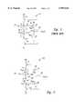
- FIG. 3is a block diagram of a memory device including the bias and equilibration voltage generator circuit of FIG. 2.
- FIG. 4is a block diagram of a computer system including the memory device of FIG. 4.
- FIG. 2is a schematic of a bias and equilibration voltage generator circuit 100 according to one embodiment of the present invention.
- the voltage generator circuit 100includes an improved bias circuit 102 which reduces the voltage differential between the bias nodes 14 and 20 and ensures that drive MOS transistors 24 and 28 do not simultaneously present low resistances for the reasons previously discussed with reference to FIG. 1.
- the bias circuit 102includes a PMOS diode-coupled transistor 104 and an NMOS diode-coupled transistor 106 coupled respectively between the control nodes 14 and 20.
- the back-bias voltage terminal of the PMOS diode-coupled transistor 104is coupled to the bias node 14, causing the source-substrate voltage of the transistor 104 to be approximately zero.
- the PMOS diode-coupled transistor 104has a threshold voltage V' tp1 corresponding to the threshold voltage for zero source-substrate voltage.
- the NMOS diode-coupled transistor 106has its source coupled to the bias node 20, its drain coupled to a tracking node 105, and its back-bias voltage terminal (not shown in FIG. 2) typically coupled to a negative voltage source or to ground.
- the transistorhas a reduced threshold voltage V' tn1 relative to the threshold voltage V tn1 of the diode-coupled transistor 16.
- the threshold voltage V' tn1is reduced due to a corresponding reduction in the source-substrate voltage of the transistor 106.
- the source-substrate voltage of the transistor 106is reduced relative to the transistor 16 of the prior art circuit 10 because the positions of the PMOS transistor 104 and the NMOS transistor 106 are reversed relative to the positions of the PMOS transistor 18 and the NMOS transistor 16 in the prior art circuit 10.
- the source of the transistor 106is at a voltage that is V' tp1 lower than the voltage on the source of the transistor 16 in the prior art circuit 10 of FIG. 1.
- the reduced source voltagereduces the source-to-substrate voltage, thereby reducing the threshold voltage of the NMOS transistor 106.
- the reduced threshold voltage V' tn1 of the NMOS diode-coupled transistor 106ensures the threshold voltages of the transistors 24. 28, 104, and 106 satisfy the relationship V' tp1 +V' tn1 ⁇ V tn2 +V tp2 as required to prevent the drive transistors 24 and 28 from simultaneously presenting low resistances.
- the reduction in the threshold voltage V' tn1 of the NMOS diode-coupled transistor 106is accomplished without requiring additional process steps while forming the voltage generator circuit 100.
- the voltage generator circuit 100is formed in a p-type semiconductor substrate.
- the PMOS transistor 104has its source coupled to the n-well to minimize the threshold voltage V' tp1 .
- the circuit 100may also be formed in an n-type semiconductor substrate.
- the NMOS transistor 106is formed in a p-well with its source coupled to the p-well, and the substrate of the PMOS transistor 104 would typically be coupled to the supply voltage V CC .
- FIG. 3is a block diagram of a memory device 150 including the voltage generator circuit 100.
- the memory device 150includes a memory-cell array 152 having a number of memory cells 154 arranged in rows and columns. one of which is shown.
- the memory-cell array 152further includes a word line WL associated with each row of memory cells 154, and a pair of complementary digit lines DL and DL associated with each column of memory cells, as shown for the illustrated memory cell 154.
- Each memory cell 154includes an access transistor 156 having its gate coupled to the associated word line WL, its drain coupled to one of the associated digit lines DL and DL, and its source coupled to one terminal of an associated storage capacitor 158. The other terminal of the storage capacitor 158 receives the output voltage V CC /2 from the voltage generator circuit 100.
- the voltage generator circuit 100also provides the reference voltage V CC /2 to a number of equilibration circuits 156 in the memory-cell array 152, one of which is shown.
- Each equilibration circuit 156is coupled between the digit lines DL and DL associated with a column of memory cells, and includes transistors 160 and 162 coupled as shown to receive the reference voltage V CC /2 and an equilibration signal EQ.
- the transistors 160 and 162turn ON coupling the digit lines DL and DL to the reference voltage V CC /2 and biasing the digit lines at this voltage.
- the detailed illustration of the memory cell 154 and equilibration circuit 156are merely to illustrate a typical application of the voltage generator circuit 100 in the memory device 150.
- One skilled in the artwill understand the operation of these components during data transfer operations of the memory device 150, and thus, for the sake of brevity, a more detailed explanation of these components during such data transfer operations is not provided.
- the memory device 150further includes an address decoder 164 which receives an address on an address bus, decodes that address, and activates the memory cell corresponding to the decoded memory address.
- a control circuit 166receives control signals on a control bus and controls operation of the memory-cell array 152 during data transfer operations.
- a read/write circuit 168is coupled to a data bus and transfers data between the data bus and the memory-cell array 152 during read/write data transfer operations.
- external circuitryprovides address, control, and data signals on respective busses to the memory device 150.
- the external circuitryprovides a memory address on the address bus and control signals on the control bus.
- the address decoder 164provides a decoded memory address to the memory-cell array 152 while the control circuit 166 provides control signals to the memory-cell array 152 in response to the control signals on the control bus.
- the control signals from the control circuit 166control the memory-cell array 152 so that the memory-cell array provides the addressed data to the read/write circuit 168.
- the read/write circuit 168then provides this data on the data bus for use by the external circuitry.
- the external circuitryprovides a memory address on the address bus, control signals on the control bus, and data on the data bus.
- the address decoder 164decodes the memory address on the address bus and provides a decoded address to the memory-cell array 152.
- the read/write circuit 168provides the data on the data bus to the memory-cell array 152 and this data is stored in the addressed memory cells in the memory-cell array 152 under control of the control circuit 166.
- FIG. 4is a block diagram of a computer system 200 including the memory device 150 of FIG. 3.
- the computer system 200includes computer circuitry 202 for performing various computing functions, such as executing specific software to perform specific calculations or tasks.
- the computer system 200includes one or more input devices 204, such as a keyboard or a mouse, coupled to the computer circuitry 202 to allow an operator to interface with the computer system 200.
- the computer system 200also includes one or more output devices 206 coupled to the computer circuitry 202, such output devices typically being a printer or a video terminal.
- One or more data storage devices 208are also typically coupled to the computer circuitry 202 to store data or retrieve data from external storage media (not shown).
- Examples of typical data storage devices 208include hard and floppy disks, tape cassettes, and compact disk read only memories ("CD-ROMs").
- the computer circuitry 202is typically coupled to the memory device 150 through a control bus, a data bus, and an address bus to provide for writing data to and reading data from the memory device 150.
Landscapes
- Engineering & Computer Science (AREA)
- Physics & Mathematics (AREA)
- Microelectronics & Electronic Packaging (AREA)
- Nonlinear Science (AREA)
- Electromagnetism (AREA)
- General Physics & Mathematics (AREA)
- Radar, Positioning & Navigation (AREA)
- Automation & Control Theory (AREA)
- Semiconductor Integrated Circuits (AREA)
- Dram (AREA)
Abstract
Description
Claims (29)
Priority Applications (2)
| Application Number | Priority Date | Filing Date | Title |
|---|---|---|---|
| US08/989,698US5959444A (en) | 1997-12-12 | 1997-12-12 | MOS transistor circuit and method for biasing a voltage generator |
| US09/260,184US6026033A (en) | 1997-12-12 | 1999-03-01 | MOS transistor circuit and method for biasing a voltage generator |
Applications Claiming Priority (1)
| Application Number | Priority Date | Filing Date | Title |
|---|---|---|---|
| US08/989,698US5959444A (en) | 1997-12-12 | 1997-12-12 | MOS transistor circuit and method for biasing a voltage generator |
Related Child Applications (1)
| Application Number | Title | Priority Date | Filing Date |
|---|---|---|---|
| US09/260,184DivisionUS6026033A (en) | 1997-12-12 | 1999-03-01 | MOS transistor circuit and method for biasing a voltage generator |
Publications (1)
| Publication Number | Publication Date |
|---|---|
| US5959444Atrue US5959444A (en) | 1999-09-28 |
Family
ID=25535382
Family Applications (2)
| Application Number | Title | Priority Date | Filing Date |
|---|---|---|---|
| US08/989,698Expired - LifetimeUS5959444A (en) | 1997-12-12 | 1997-12-12 | MOS transistor circuit and method for biasing a voltage generator |
| US09/260,184Expired - LifetimeUS6026033A (en) | 1997-12-12 | 1999-03-01 | MOS transistor circuit and method for biasing a voltage generator |
Family Applications After (1)
| Application Number | Title | Priority Date | Filing Date |
|---|---|---|---|
| US09/260,184Expired - LifetimeUS6026033A (en) | 1997-12-12 | 1999-03-01 | MOS transistor circuit and method for biasing a voltage generator |
Country Status (1)
| Country | Link |
|---|---|
| US (2) | US5959444A (en) |
Cited By (6)
| Publication number | Priority date | Publication date | Assignee | Title |
|---|---|---|---|---|
| US6087813A (en)* | 1998-11-19 | 2000-07-11 | Mitsubishi Denki Kabushiki Kaisha | Internal voltage generation circuit capable of stably generating internal voltage with low power consumption |
| US6265858B1 (en)* | 1999-07-28 | 2001-07-24 | Hyundai Electronics Industries Co., Ltd. | Voltage adjusting circuit |
| US6320453B1 (en) | 1998-02-18 | 2001-11-20 | Micron Technology, Inc. | Method and circuit for lowering standby current in an integrated circuit |
| US20040189345A1 (en)* | 2003-03-28 | 2004-09-30 | Industrial Technology Research Institute | Mixed-voltage I/O design with novel floating N-well and gate-tracking circuits |
| US20050007190A1 (en)* | 2002-04-17 | 2005-01-13 | Renesas Technology Corp. | Potential generating circuit capable of correctly controlling output potential |
| US20120140413A1 (en)* | 2009-07-08 | 2012-06-07 | Callisto France | Dual-performance low noise amplifier for satellite-based radiofrequency communication |
Families Citing this family (2)
| Publication number | Priority date | Publication date | Assignee | Title |
|---|---|---|---|---|
| US7782731B2 (en)* | 2001-07-23 | 2010-08-24 | Joseph Reid Henrichs | Optical hard disk drive having a phase-change microhead array chip |
| US9774324B2 (en)* | 2014-12-05 | 2017-09-26 | Intel Corporation | Biasing scheme for high voltage circuits using low voltage devices |
Citations (10)
| Publication number | Priority date | Publication date | Assignee | Title |
|---|---|---|---|---|
| US34290A (en)* | 1862-02-04 | Improvement in construction of walls of buildings | ||
| US4663584A (en)* | 1985-06-10 | 1987-05-05 | Kabushiki Kaisha Toshiba | Intermediate potential generation circuit |
| US4670706A (en)* | 1985-03-27 | 1987-06-02 | Mitsubishi Denki Kabushiki Kaisha | Constant voltage generating circuit |
| US4788455A (en)* | 1985-08-09 | 1988-11-29 | Mitsubishi Denki Kabushiki Kaisha | CMOS reference voltage generator employing separate reference circuits for each output transistor |
| US4812735A (en)* | 1987-01-14 | 1989-03-14 | Kabushiki Kaisha Toshiba | Intermediate potential generating circuit |
| US4906914A (en)* | 1987-12-18 | 1990-03-06 | Kabushiki Kaisha Toshiba | Intermediate potential generation circuit for generating a potential intermediate between a power source potential and ground potential |
| US5008609A (en)* | 1989-06-06 | 1991-04-16 | Mitsubishi Denki Kabushiki Kaisha | Voltage generating circuit for semiconductor device |
| US5369354A (en)* | 1992-10-14 | 1994-11-29 | Mitsubishi Denki Kabushiki Kaisha | Intermediate voltage generating circuit having low output impedance |
| US5717324A (en)* | 1995-12-11 | 1998-02-10 | Mitsubishi Denki Kabushiki Kaisha | Intermediate potential generation circuit |
| US5757225A (en)* | 1995-09-04 | 1998-05-26 | Mitsubishi Denki Kabushiki Kaisha | Voltage generation circuit that can stably generate intermediate potential independent of threshold voltage |
Family Cites Families (4)
| Publication number | Priority date | Publication date | Assignee | Title |
|---|---|---|---|---|
| KR940017214A (en)* | 1992-12-24 | 1994-07-26 | 가나이 쓰토무 | Reference voltage generator |
| JPH06223568A (en)* | 1993-01-29 | 1994-08-12 | Mitsubishi Electric Corp | Intermediate potential generator |
| KR0142970B1 (en)* | 1995-06-24 | 1998-08-17 | 김광호 | Reference voltage generation circuit of semiconductor memory device |
| DE19602125C2 (en)* | 1996-01-22 | 1998-03-12 | Siemens Ag | Circuit simulation method for computer-aided determination of the transient response of a quartz resonator circuit |
- 1997
- 1997-12-12USUS08/989,698patent/US5959444A/ennot_activeExpired - Lifetime
- 1999
- 1999-03-01USUS09/260,184patent/US6026033A/ennot_activeExpired - Lifetime
Patent Citations (13)
| Publication number | Priority date | Publication date | Assignee | Title |
|---|---|---|---|---|
| US34290A (en)* | 1862-02-04 | Improvement in construction of walls of buildings | ||
| USRE34290E (en) | 1985-03-27 | 1993-06-22 | Mitsubishi Denki K.K. | Constant voltage generating circuit |
| US4670706A (en)* | 1985-03-27 | 1987-06-02 | Mitsubishi Denki Kabushiki Kaisha | Constant voltage generating circuit |
| US4670706B1 (en)* | 1985-03-27 | 1989-07-25 | ||
| US4663584A (en)* | 1985-06-10 | 1987-05-05 | Kabushiki Kaisha Toshiba | Intermediate potential generation circuit |
| US4663584B1 (en)* | 1985-06-10 | 1996-05-21 | Toshiba Kk | Intermediate potential generation circuit |
| US4788455A (en)* | 1985-08-09 | 1988-11-29 | Mitsubishi Denki Kabushiki Kaisha | CMOS reference voltage generator employing separate reference circuits for each output transistor |
| US4812735A (en)* | 1987-01-14 | 1989-03-14 | Kabushiki Kaisha Toshiba | Intermediate potential generating circuit |
| US4906914A (en)* | 1987-12-18 | 1990-03-06 | Kabushiki Kaisha Toshiba | Intermediate potential generation circuit for generating a potential intermediate between a power source potential and ground potential |
| US5008609A (en)* | 1989-06-06 | 1991-04-16 | Mitsubishi Denki Kabushiki Kaisha | Voltage generating circuit for semiconductor device |
| US5369354A (en)* | 1992-10-14 | 1994-11-29 | Mitsubishi Denki Kabushiki Kaisha | Intermediate voltage generating circuit having low output impedance |
| US5757225A (en)* | 1995-09-04 | 1998-05-26 | Mitsubishi Denki Kabushiki Kaisha | Voltage generation circuit that can stably generate intermediate potential independent of threshold voltage |
| US5717324A (en)* | 1995-12-11 | 1998-02-10 | Mitsubishi Denki Kabushiki Kaisha | Intermediate potential generation circuit |
Cited By (11)
| Publication number | Priority date | Publication date | Assignee | Title |
|---|---|---|---|---|
| US6320453B1 (en) | 1998-02-18 | 2001-11-20 | Micron Technology, Inc. | Method and circuit for lowering standby current in an integrated circuit |
| US6373755B1 (en)* | 1998-02-18 | 2002-04-16 | Micron Technology, Inc. | Method and circuit for lowering standby current in an integrated circuit |
| US6462610B1 (en) | 1998-02-18 | 2002-10-08 | Micron Technology, Inc. | Method and circuit for lowering standby current in an integrated circuit |
| US6087813A (en)* | 1998-11-19 | 2000-07-11 | Mitsubishi Denki Kabushiki Kaisha | Internal voltage generation circuit capable of stably generating internal voltage with low power consumption |
| US6265858B1 (en)* | 1999-07-28 | 2001-07-24 | Hyundai Electronics Industries Co., Ltd. | Voltage adjusting circuit |
| US20050007190A1 (en)* | 2002-04-17 | 2005-01-13 | Renesas Technology Corp. | Potential generating circuit capable of correctly controlling output potential |
| US6937088B2 (en)* | 2002-04-17 | 2005-08-30 | Renesas Technology Corp. | Potential generating circuit capable of correctly controlling output potential |
| US20040189345A1 (en)* | 2003-03-28 | 2004-09-30 | Industrial Technology Research Institute | Mixed-voltage I/O design with novel floating N-well and gate-tracking circuits |
| US6838908B2 (en)* | 2003-03-28 | 2005-01-04 | Industrial Technology Research Institute | Mixed-voltage I/O design with novel floating N-well and gate-tracking circuits |
| US20120140413A1 (en)* | 2009-07-08 | 2012-06-07 | Callisto France | Dual-performance low noise amplifier for satellite-based radiofrequency communication |
| US8885340B2 (en)* | 2009-07-08 | 2014-11-11 | Callisto France | Dual-performance low noise amplifier for satellite-based radiofrequency communication |
Also Published As
| Publication number | Publication date |
|---|---|
| US6026033A (en) | 2000-02-15 |
Similar Documents
| Publication | Publication Date | Title |
|---|---|---|
| US5726946A (en) | Semiconductor integrated circuit device having hierarchical power source arrangement | |
| EP0136811B1 (en) | Bit line load and column circuitry for a semiconductor memory | |
| US7382674B2 (en) | Static random access memory (SRAM) with clamped source potential in standby mode | |
| US5436552A (en) | Clamping circuit for clamping a reference voltage at a predetermined level | |
| US6044011A (en) | Static-random-access-memory cell | |
| JP3085073B2 (en) | Static RAM | |
| KR0155078B1 (en) | Semiconductor circuit having cmos circuit for use in strong electric field | |
| US5404329A (en) | Boosting circuit improved to operate in a wider range of power supply voltage, and a semiconductor memory and a semiconductor integrated circuit device using the same | |
| CN101286360A (en) | semiconductor integrated circuit | |
| US6493282B2 (en) | Semiconductor integrated circuit | |
| GB2162394A (en) | Mos static ram | |
| US5708599A (en) | Semiconductor memory device capable of reducing power consumption | |
| KR100468549B1 (en) | Circuit comprising a decoder and a plurality of drive circuits | |
| US5373473A (en) | Amplifier circuit and semiconductor memory device employing the same | |
| US5959444A (en) | MOS transistor circuit and method for biasing a voltage generator | |
| US4860257A (en) | Level shifter for an input/output bus in a CMOS dynamic ram | |
| US5677889A (en) | Static type semiconductor device operable at a low voltage with small power consumption | |
| US6707707B2 (en) | SRAM power-up system and method | |
| EP0411818B1 (en) | Current sensing amplifier for a memory | |
| US5973975A (en) | Method and circuit for sharing sense amplifier drivers | |
| JP4259739B2 (en) | Semiconductor memory device | |
| KR0126908B1 (en) | Static semiconductor memory device | |
| EP0462866B1 (en) | Semiconductor memory device | |
| KR100190366B1 (en) | Semiconductor memory device and power supply method | |
| EP0200500A2 (en) | CMOS memory bias systems |
Legal Events
| Date | Code | Title | Description |
|---|---|---|---|
| AS | Assignment | Owner name:MICRON TECHNOLOGY, INC., IDAHO Free format text:ASSIGNMENT OF ASSIGNORS INTEREST;ASSIGNOR:CASPER, STEPHEN L.;REEL/FRAME:009228/0602 Effective date:19980526 | |
| STCF | Information on status: patent grant | Free format text:PATENTED CASE | |
| FEPP | Fee payment procedure | Free format text:PAYER NUMBER DE-ASSIGNED (ORIGINAL EVENT CODE: RMPN); ENTITY STATUS OF PATENT OWNER: LARGE ENTITY Free format text:PAYOR NUMBER ASSIGNED (ORIGINAL EVENT CODE: ASPN); ENTITY STATUS OF PATENT OWNER: LARGE ENTITY | |
| FPAY | Fee payment | Year of fee payment:4 | |
| FPAY | Fee payment | Year of fee payment:8 | |
| FPAY | Fee payment | Year of fee payment:12 | |
| AS | Assignment | Owner name:U.S. BANK NATIONAL ASSOCIATION, AS COLLATERAL AGENT, CALIFORNIA Free format text:SECURITY INTEREST;ASSIGNOR:MICRON TECHNOLOGY, INC.;REEL/FRAME:038669/0001 Effective date:20160426 Owner name:U.S. BANK NATIONAL ASSOCIATION, AS COLLATERAL AGEN Free format text:SECURITY INTEREST;ASSIGNOR:MICRON TECHNOLOGY, INC.;REEL/FRAME:038669/0001 Effective date:20160426 | |
| AS | Assignment | Owner name:MORGAN STANLEY SENIOR FUNDING, INC., AS COLLATERAL AGENT, MARYLAND Free format text:PATENT SECURITY AGREEMENT;ASSIGNOR:MICRON TECHNOLOGY, INC.;REEL/FRAME:038954/0001 Effective date:20160426 Owner name:MORGAN STANLEY SENIOR FUNDING, INC., AS COLLATERAL Free format text:PATENT SECURITY AGREEMENT;ASSIGNOR:MICRON TECHNOLOGY, INC.;REEL/FRAME:038954/0001 Effective date:20160426 | |
| AS | Assignment | Owner name:U.S. BANK NATIONAL ASSOCIATION, AS COLLATERAL AGENT, CALIFORNIA Free format text:CORRECTIVE ASSIGNMENT TO CORRECT THE REPLACE ERRONEOUSLY FILED PATENT #7358718 WITH THE CORRECT PATENT #7358178 PREVIOUSLY RECORDED ON REEL 038669 FRAME 0001. ASSIGNOR(S) HEREBY CONFIRMS THE SECURITY INTEREST;ASSIGNOR:MICRON TECHNOLOGY, INC.;REEL/FRAME:043079/0001 Effective date:20160426 Owner name:U.S. BANK NATIONAL ASSOCIATION, AS COLLATERAL AGEN Free format text:CORRECTIVE ASSIGNMENT TO CORRECT THE REPLACE ERRONEOUSLY FILED PATENT #7358718 WITH THE CORRECT PATENT #7358178 PREVIOUSLY RECORDED ON REEL 038669 FRAME 0001. ASSIGNOR(S) HEREBY CONFIRMS THE SECURITY INTEREST;ASSIGNOR:MICRON TECHNOLOGY, INC.;REEL/FRAME:043079/0001 Effective date:20160426 | |
| AS | Assignment | Owner name:MICRON TECHNOLOGY, INC., IDAHO Free format text:RELEASE BY SECURED PARTY;ASSIGNOR:U.S. BANK NATIONAL ASSOCIATION, AS COLLATERAL AGENT;REEL/FRAME:047243/0001 Effective date:20180629 | |
| AS | Assignment | Owner name:MICRON TECHNOLOGY, INC., IDAHO Free format text:RELEASE BY SECURED PARTY;ASSIGNOR:MORGAN STANLEY SENIOR FUNDING, INC., AS COLLATERAL AGENT;REEL/FRAME:050937/0001 Effective date:20190731 |