US5958100A - Process of making a glass semiconductor package - Google Patents
Process of making a glass semiconductor packageDownload PDFInfo
- Publication number
- US5958100A US5958100AUS08/692,883US69288396AUS5958100AUS 5958100 AUS5958100 AUS 5958100AUS 69288396 AUS69288396 AUS 69288396AUS 5958100 AUS5958100 AUS 5958100A
- Authority
- US
- United States
- Prior art keywords
- glass
- group
- magnesium
- semiconductor package
- sealing
- Prior art date
- Legal status (The legal status is an assumption and is not a legal conclusion. Google has not performed a legal analysis and makes no representation as to the accuracy of the status listed.)
- Expired - Lifetime
Links
Images


Classifications
- H—ELECTRICITY
- H01—ELECTRIC ELEMENTS
- H01L—SEMICONDUCTOR DEVICES NOT COVERED BY CLASS H10
- H01L23/00—Details of semiconductor or other solid state devices
- H01L23/28—Encapsulations, e.g. encapsulating layers, coatings, e.g. for protection
- H01L23/29—Encapsulations, e.g. encapsulating layers, coatings, e.g. for protection characterised by the material, e.g. carbon
- H01L23/291—Oxides or nitrides or carbides, e.g. ceramics, glass
- H—ELECTRICITY
- H01—ELECTRIC ELEMENTS
- H01L—SEMICONDUCTOR DEVICES NOT COVERED BY CLASS H10
- H01L2224/00—Indexing scheme for arrangements for connecting or disconnecting semiconductor or solid-state bodies and methods related thereto as covered by H01L24/00
- H01L2224/01—Means for bonding being attached to, or being formed on, the surface to be connected, e.g. chip-to-package, die-attach, "first-level" interconnects; Manufacturing methods related thereto
- H01L2224/42—Wire connectors; Manufacturing methods related thereto
- H01L2224/47—Structure, shape, material or disposition of the wire connectors after the connecting process
- H01L2224/48—Structure, shape, material or disposition of the wire connectors after the connecting process of an individual wire connector
- H01L2224/4805—Shape
- H01L2224/4809—Loop shape
- H01L2224/48091—Arched
- H—ELECTRICITY
- H01—ELECTRIC ELEMENTS
- H01L—SEMICONDUCTOR DEVICES NOT COVERED BY CLASS H10
- H01L24/00—Arrangements for connecting or disconnecting semiconductor or solid-state bodies; Methods or apparatus related thereto
- H01L24/01—Means for bonding being attached to, or being formed on, the surface to be connected, e.g. chip-to-package, die-attach, "first-level" interconnects; Manufacturing methods related thereto
- H01L24/42—Wire connectors; Manufacturing methods related thereto
- H01L24/47—Structure, shape, material or disposition of the wire connectors after the connecting process
- H01L24/48—Structure, shape, material or disposition of the wire connectors after the connecting process of an individual wire connector
- H—ELECTRICITY
- H01—ELECTRIC ELEMENTS
- H01L—SEMICONDUCTOR DEVICES NOT COVERED BY CLASS H10
- H01L2924/00—Indexing scheme for arrangements or methods for connecting or disconnecting semiconductor or solid-state bodies as covered by H01L24/00
- H01L2924/0001—Technical content checked by a classifier
- H01L2924/00014—Technical content checked by a classifier the subject-matter covered by the group, the symbol of which is combined with the symbol of this group, being disclosed without further technical details
- H—ELECTRICITY
- H01—ELECTRIC ELEMENTS
- H01L—SEMICONDUCTOR DEVICES NOT COVERED BY CLASS H10
- H01L2924/00—Indexing scheme for arrangements or methods for connecting or disconnecting semiconductor or solid-state bodies as covered by H01L24/00
- H01L2924/01—Chemical elements
- H01L2924/01012—Magnesium [Mg]
- H—ELECTRICITY
- H01—ELECTRIC ELEMENTS
- H01L—SEMICONDUCTOR DEVICES NOT COVERED BY CLASS H10
- H01L2924/00—Indexing scheme for arrangements or methods for connecting or disconnecting semiconductor or solid-state bodies as covered by H01L24/00
- H01L2924/01—Chemical elements
- H01L2924/01079—Gold [Au]
- H—ELECTRICITY
- H01—ELECTRIC ELEMENTS
- H01L—SEMICONDUCTOR DEVICES NOT COVERED BY CLASS H10
- H01L2924/00—Indexing scheme for arrangements or methods for connecting or disconnecting semiconductor or solid-state bodies as covered by H01L24/00
- H01L2924/095—Indexing scheme for arrangements or methods for connecting or disconnecting semiconductor or solid-state bodies as covered by H01L24/00 with a principal constituent of the material being a combination of two or more materials provided in the groups H01L2924/013 - H01L2924/0715
- H01L2924/097—Glass-ceramics, e.g. devitrified glass
- H01L2924/09701—Low temperature co-fired ceramic [LTCC]
- H—ELECTRICITY
- H01—ELECTRIC ELEMENTS
- H01L—SEMICONDUCTOR DEVICES NOT COVERED BY CLASS H10
- H01L2924/00—Indexing scheme for arrangements or methods for connecting or disconnecting semiconductor or solid-state bodies as covered by H01L24/00
- H01L2924/10—Details of semiconductor or other solid state devices to be connected
- H01L2924/11—Device type
- H01L2924/14—Integrated circuits
- H—ELECTRICITY
- H01—ELECTRIC ELEMENTS
- H01L—SEMICONDUCTOR DEVICES NOT COVERED BY CLASS H10
- H01L2924/00—Indexing scheme for arrangements or methods for connecting or disconnecting semiconductor or solid-state bodies as covered by H01L24/00
- H01L2924/15—Details of package parts other than the semiconductor or other solid state devices to be connected
- H01L2924/181—Encapsulation
- Y—GENERAL TAGGING OF NEW TECHNOLOGICAL DEVELOPMENTS; GENERAL TAGGING OF CROSS-SECTIONAL TECHNOLOGIES SPANNING OVER SEVERAL SECTIONS OF THE IPC; TECHNICAL SUBJECTS COVERED BY FORMER USPC CROSS-REFERENCE ART COLLECTIONS [XRACs] AND DIGESTS
- Y10—TECHNICAL SUBJECTS COVERED BY FORMER USPC
- Y10S—TECHNICAL SUBJECTS COVERED BY FORMER USPC CROSS-REFERENCE ART COLLECTIONS [XRACs] AND DIGESTS
- Y10S65/00—Glass manufacturing
- Y10S65/11—Encapsulating
Definitions
- This inventionrelates to processes of making semiconductor packages, and more particularly to processes of making glass hermetically sealed semiconductor packages.
- hermetic packagesare generally formed from ceramic or metal components bonded together and hermetically sealed with glass or metal.
- Nonhermetic packagesare generally formed from ceramic, metal or plastic components and are usually bonded together and sealed with epoxy.
- Nonhermetic packagesare also formed by molding a plastic body about the semiconductor device.
- a typical ceramic type hermetic packageis illustrated in Karpman, U.S. Pat. No. 5,117,279. Examples of nonhermetic molded plastic and epoxy sealed packages are illustrated in Nambu et al., U.S. Pat. No. 4,777,520 and Mahulikar et al., U.S. Pat. No. 5,155,299, respectively.
- the hermetic packages presently in useare much more expensive to produce or procure than are nonhermetic packages.
- Package costis particularly important for high density surface mounting, automated mounting and other forms of mass production and assembly of printed circuit boards.
- Nonhermetic molded plastic packagesare the least costly to produce and have been widely adopted for use in mass production of large scale integrated circuits and other semiconductor devices.
- Plastic packages, however, like other nonhermetic packages,are not adequate for many semiconductor applications because they do not adequately protect the semiconductor device from its operating environment.
- molded plastic packageshave insufficient thermal conductivity for use in higher power circuits that generate a large quantity of heat during operation. It is desireable to combine the low production/procurement cost and versatility of molded plastic packages with the hermeticity and high thermal conductivity of ceramic or metal glass sealed hermetic packages.
- hermetic seals in ceramic packagesoften require high temperature processing. For example, high temperatures are often necessary to form a hermetic glass seal between the base and lid of the ceramic package housing.
- the glass sealing processis typically performed at temperatures of 400° C. to 500° C. and heating times of one to two hours. The relatively high temperatures and heating times are required to cause the glass layer to flow to form the hermetic seal.
- the high temperature sealing processcan cause oxidation of metals used to form electrical leads and other semiconductor components.
- FischerU.S. Pat. No. 3,596,136, discloses a glass dome formed of moldable glass for increasing the transmission of the electrolumniscent light emitted by a diode.
- the process disclosed in Fischer for molding the glass over the diodedoes not seal the diode from the external environment.
- Fischeris disadvantageous, particularly for mass production, because the device or mold is heated to melt the solid glass bead that is placed on the device or into the mold.
- a moldable glass semiconductor packagehas been invented using these new low sealing temperature glasses.
- the inventioncombines the hermeticity of glass sealed ceramic packages with the low cost, ease of manufacture and versatility of molded plastic packages. Although these glass packages are not wholly impervious to moisture and, therefore, not totally hermetic, the glass remains impervious to moisture beyond the useful life of most semiconductor devices, including those used in military operations under the most demanding operating conditions and performance requirements. Consequently, these glass packages, as a practical matter, provide a hermetic seal for the life of the semiconductor device packaged therein.
- the general purpose and principal object of the inventionis to provide a process of making a hermetically sealed moldable glass semiconductor package that is less costly than ceramic and metal packages.
- Another objectis to provide a process of making a hermetically sealed moldable glass semiconductor package using glasses having a sealing temperature not over 350° C. and a CTE not over 110 ⁇ 10 -7 /°C.
- Another objectis to provide a process of making a glass semiconductor package that can accommodate various sizes of semiconductor and other electronic devices and elements.
- Another objectis to provide a process of making a vibration resistance semiconductor package to reduce bondwire breakage and joint crackage at electrical connections.
- Another objectis to provide a process of making a semiconductor package whose coefficient of thermal expansion can be varied so as to be compatible with different semiconductor devices and substrate materials.
- Another objectis to provide a process of making a glass semiconductor package that eliminates the sealing process used for ceramic packages to reduce porosity in the ceramic package materials.
- Another objectis to provide a process of making a semiconductor package that does not require the use of quartz or other fillers presently used in epoxy/plastic packages and thereby eliminate the risk of damaging bondwires, electrical connections and other components of the semiconductor device caused by filler particles.
- a process of making glass semiconductor packageswhich comprises encapsulating or overlaying an electronic device with a body of molten thermoplastic glass that is solidified by cooling.
- the body of moldable thermoplastic glassmay be formed by variety of processes, such as injection molding, cerdip or blob top chip coating.
- the moldable thermoplastic glassis impervious to moisture for the useable life of the electronic device, has a sealing temperature not over 350° C. and has a coefficient of thermal expansion not over 110 ⁇ 10 -7 /°C.
- the moldable glassmay be either tin-phosphorus oxyfluoride sealing glass or lead sealing glass.
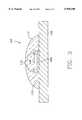
- FIG. 1is a cross-section view of a glass semiconductor package formed using the preferred embodiment of the invention.
- FIG. 2is a top view of a leadframe assembly.
- FIG. 3is a cross-section view of a glass blob top semiconductor package formed using another embodiment of the invention.
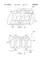
- FIG. 4is a top perspective view of a glass cerdip single in line memory module (SIMM) semiconductor package formed using another embodiment of the invention.
- SIMMsingle in line memory module
- FIG. 5is a top view of a glass blob top single in line memory module (SIMM) semiconductor package illustrating the use of another embodiment of the invention.
- SIMMsingle in line memory module
- FIG. 1is a cross-section of a glass semiconductor package 2 fabricated using the method of the present invention.
- a die 4representing a semiconductor, integrated circuit or other electronic device, is mounted on and bonded to a substrate 6 by a bonding layer 8.
- a plurality of external leads 10are disposed around the perimeter of the die 4. Each external lead 10 has an inner end 12 and an outer end 14. Bondwires 16 electrically connect the die 4 to the inner end 12 of each external lead 10.
- the die 4, substrate 6, bonding layer 8 and inner end 12 of each external lead 10are encapsulated in a body 18 of molten glass that solidfies as it cools to form the glass semiconductor package 2.
- the bondwires 16may be connected to the die 4 and the inner end 12 of each external lead 10 in any conventional manner such as soldering, gold ball bonding or wedge bonding.
- the substrate 6may be made of any suitable material such as fiberglass reinforced board or the die attach pad on a standard leadframe.
- the bonding layer 8may be made of thermal epoxy, thermal resin, sealing glass or other suitable material. Preferably, the bonding layer 8 has a sealing temperature above the sealing temperature of the body 18.
- the body 18is made of moldable thermoplastic glass having a sealing temperature not over 350° C. and a CTE not over 110 ⁇ 10 -7 .
- the glassmay be either tin-phosphorus oxyfluoride glass of the type described in U.S. Pat. No. 5,089,446, incorporated herein by reference, or lead glass of the type described in U.S. Pat. No. 5,089,445, incorporated herein by reference.
- the CTEs of these glassesmay be varied by changing the type and quantity of additives to the base materials to match the CTEs of the components of different types of electronic devices to be packaged. This ability to match CTEs reduces the risk of damaging the electronic device during packaging and, thereby, increases the reliability of such devices. Further, the low sealing temperatures of these glasses minimizes damage to and oxidation of electrical leads and other semiconductor components.
- a prefabricated leadframe 20includes substrate 6, external leads 10 and leadframe rails 22.
- Die 4is mounted on and bonded to substrate 6 with a bonding layer 8 made of thermal epoxy, thermal resin, sealing glass or other suitable material, to form a leadframe assembly 24.
- Die 4is then electrically connected to the inner end 12 of the external leads 10 by bondwires 16.
- bondwires 16can be electrically connected to the inner end 12 of the external leads 10 by a wire bond (as shown), by a tape-automated-bond (TAB) bond or by bonding directly to the external leads 10.
- TABtape-automated-bond
- the leadframe assembly 24is placed into a mold shaped to form a body 18.
- Molten thermoplastic glasshaving a sealing temperature of not more than 350° C. and a CTE of not more than 110 ⁇ 10 -7 is melted and injected into the mold.
- the molten glassis then allowed to cool (or actively cooled) and solidify to form the body 18 which encapsulates the die 4, substrate 6, bondwires 16 and inner end 12 of the external leads 10.
- the leadframe assembly 24is then removed from the mold and the leadframe rails 22 severed from the other components, leaving the completed glass semiconductor package 2.
- This process of making glass semiconductor packagesis particularly advantageous because it may be implemented with fixtures and injection molding equipment currently used for molded thermoset plastic packages or injection molding equipment currently used in the plastics industries.
- FIG. 3illustrates a blob top glass semiconductor package 102.
- a die 104is mounted and bonded to a substrate 106 by a bonding layer 108.
- Substrate 106has a metalized surface 110.
- Bondwires 112electrically connect the die 104 with the metalized surface 110 of the substrate 108.
- the die 104, bonding layer 108 and bondwires 112are encapsulated in a body 114.
- the body 114is formed by overlaying the die 104 and bondwires 112 with a blob of molten glass which solidifies as it cools.
- the body 114is made of glass having a sealing temperature not over 350° C. and a CTE not over 110 ⁇ 10 -7 , and may consist of the tin-phosphorus oxyfluoride or lead glasses referenced above.
- FIG. 4illustrates a glass semiconductor package 202 formed by immersing a single in line memory module (SIMM) 204 or similar assembly in molten glass of the type previously described.
- a plurality of electronic devices 206are mounted on a substrate 208.
- a plurality of electrical contacts 210corresponding to and located adjacent to the electronic devices 206, are mounted along the edge of the substrate 208.
- a plurality of bondwires 212electrically connect the electronic devices 206 to the contacts 210.
- the electronic devices 206 and a portion of the bondwires 212 and the substrate 208are immersed in molten glass. The glass contacting these parts cools forming a thin hermetically sealed body 214.
- the thickness of the bodymay be varied depending upon the temperature of the parts and the length and number of immersions.
- the electronic devices 206, a portion of the bondwires 212 and a portion of the substrate 206may be overlaid with a body of molten glass 216.
Landscapes
- Engineering & Computer Science (AREA)
- Chemical & Material Sciences (AREA)
- Ceramic Engineering (AREA)
- Physics & Mathematics (AREA)
- Condensed Matter Physics & Semiconductors (AREA)
- General Physics & Mathematics (AREA)
- Computer Hardware Design (AREA)
- Microelectronics & Electronic Packaging (AREA)
- Power Engineering (AREA)
- Structures Or Materials For Encapsulating Or Coating Semiconductor Devices Or Solid State Devices (AREA)
Abstract
Description
Claims (2)
Priority Applications (1)
| Application Number | Priority Date | Filing Date | Title |
|---|---|---|---|
| US08/692,883US5958100A (en) | 1993-06-03 | 1996-07-31 | Process of making a glass semiconductor package |
Applications Claiming Priority (3)
| Application Number | Priority Date | Filing Date | Title |
|---|---|---|---|
| US7258793A | 1993-06-03 | 1993-06-03 | |
| US22053494A | 1994-03-13 | 1994-03-13 | |
| US08/692,883US5958100A (en) | 1993-06-03 | 1996-07-31 | Process of making a glass semiconductor package |
Related Parent Applications (1)
| Application Number | Title | Priority Date | Filing Date |
|---|---|---|---|
| US22053494AContinuation | 1993-06-03 | 1994-03-13 |
Publications (1)
| Publication Number | Publication Date |
|---|---|
| US5958100Atrue US5958100A (en) | 1999-09-28 |
Family
ID=26753526
Family Applications (1)
| Application Number | Title | Priority Date | Filing Date |
|---|---|---|---|
| US08/692,883Expired - LifetimeUS5958100A (en) | 1993-06-03 | 1996-07-31 | Process of making a glass semiconductor package |
Country Status (1)
| Country | Link |
|---|---|
| US (1) | US5958100A (en) |
Cited By (58)
| Publication number | Priority date | Publication date | Assignee | Title |
|---|---|---|---|---|
| US6335548B1 (en) | 1999-03-15 | 2002-01-01 | Gentex Corporation | Semiconductor radiation emitter package |
| US20020066966A1 (en)* | 2000-08-17 | 2002-06-06 | Farnworth Warren M. | Stereolithographic methods for fabricating hermetic semiconductor device packages and semiconductor devices including stereolithographically fabricated hermetic packages |
| US6441943B1 (en) | 1997-04-02 | 2002-08-27 | Gentex Corporation | Indicators and illuminators using a semiconductor radiation emitter package |
| US6521916B2 (en) | 1999-03-15 | 2003-02-18 | Gentex Corporation | Radiation emitter device having an encapsulant with different zones of thermal conductivity |
| US20030042581A1 (en)* | 2001-08-29 | 2003-03-06 | Fee Setho Sing | Packaged microelectronic devices and methods of forming same |
| US6558600B1 (en) | 2000-05-04 | 2003-05-06 | Micron Technology, Inc. | Method for packaging microelectronic substrates |
| US6564979B2 (en) | 2001-07-18 | 2003-05-20 | Micron Technology, Inc. | Method and apparatus for dispensing adhesive on microelectronic substrate supports |
| US6576494B1 (en) | 2000-06-28 | 2003-06-10 | Micron Technology, Inc. | Recessed encapsulated microelectronic devices and methods for formation |
| US6622380B1 (en) | 2002-02-12 | 2003-09-23 | Micron Technology, Inc. | Methods for manufacturing microelectronic devices and methods for mounting microelectronic packages to circuit boards |
| US6639360B2 (en) | 2001-01-31 | 2003-10-28 | Gentex Corporation | High power radiation emitter device and heat dissipating package for electronic components |
| US6638595B2 (en) | 2000-06-28 | 2003-10-28 | Micron Technology, Inc. | Method and apparatus for reduced flash encapsulation of microelectronic devices |
| US6653173B2 (en) | 2000-06-16 | 2003-11-25 | Micron Technology, Inc. | Method and apparatus for packaging a microelectronic die |
| US6656769B2 (en) | 2000-05-08 | 2003-12-02 | Micron Technology, Inc. | Method and apparatus for distributing mold material in a mold for packaging microelectronic devices |
| US20030222333A1 (en)* | 2002-06-04 | 2003-12-04 | Bolken Todd O. | Sealed electronic device packages with transparent coverings |
| US20040026773A1 (en)* | 2002-08-08 | 2004-02-12 | Koon Eng Meow | Packaged microelectronic components |
| US20040026776A1 (en)* | 2002-08-08 | 2004-02-12 | Brand Joseph M. | Microelectronic devices and methods for manufacturing and operating packaged microelectronic device assemblies |
| US20040031621A1 (en)* | 2002-08-19 | 2004-02-19 | Heng Puah Kia | Packaged microelectronic component assemblies |
| US20040038447A1 (en)* | 2002-08-21 | 2004-02-26 | Corisis David J | Packaged microelectronic devices and methods for assembling microelectronic devices |
| US20040055783A1 (en)* | 2002-09-03 | 2004-03-25 | Hitachi, Ltd. | Automotive electronic control unit |
| US20040100772A1 (en)* | 2002-11-22 | 2004-05-27 | Chye Lim Thiam | Packaged microelectronic component assemblies |
| US20040113549A1 (en)* | 2001-01-31 | 2004-06-17 | Roberts John K | High power radiation emitter device and heat dissipating package for electronic components |
| US20040155331A1 (en)* | 2003-02-11 | 2004-08-12 | Blaine Thurgood | Packaged microelectronic devices and methods for packaging microelectronic devices |
| US20040173899A1 (en)* | 2003-03-04 | 2004-09-09 | Peng Neo Chee | Microelectronic component assemblies employing lead frames having reduced-thickness inner lengths |
| US6796028B2 (en) | 2000-08-23 | 2004-09-28 | Micron Technology, Inc. | Method of Interconnecting substrates for electrical coupling of microelectronic components |
| US6838760B1 (en) | 2000-08-28 | 2005-01-04 | Micron Technology, Inc. | Packaged microelectronic devices with interconnecting units |
| US20050019988A1 (en)* | 2002-04-04 | 2005-01-27 | Tongbi Jiang | Method and apparatus for attaching microelectronic substrates and support members |
| US20050093174A1 (en)* | 2003-10-31 | 2005-05-05 | Seng Eric T.S. | Reduced footprint packaged microelectronic components and methods for manufacturing such microelectronic components |
| US6921860B2 (en) | 2003-03-18 | 2005-07-26 | Micron Technology, Inc. | Microelectronic component assemblies having exposed contacts |
| US6979595B1 (en) | 2000-08-24 | 2005-12-27 | Micron Technology, Inc. | Packaged microelectronic devices with pressure release elements and methods for manufacturing and using such packaged microelectronic devices |
| US20060017177A1 (en)* | 2004-07-23 | 2006-01-26 | Seng Eric T S | Microelectronic component assemblies with recessed wire bonds and methods of making same |
| US20060046346A1 (en)* | 2004-09-01 | 2006-03-02 | Benson Peter A | Methods for packaging microfeature devices and microfeature devices formed by such methods |
| US20060043461A1 (en)* | 2002-11-20 | 2006-03-02 | Stmicroelectronics S.R.L. | Process for manufacturing a byte selection transistor for a matrix of non volatile memory cells and corresponding structure |
| US20060133044A1 (en)* | 2004-12-16 | 2006-06-22 | Seoul Semiconductor Co., Ltd. | Leadframe and packaged light emitting diode |
| US20070031998A1 (en)* | 2000-08-16 | 2007-02-08 | Micron Technology, Inc. | Method and apparatus for removing encapsulating material from a packaged microelectronic device |
| US20070148820A1 (en)* | 2005-12-22 | 2007-06-28 | Micron Technology, Inc. | Microelectronic devices and methods for manufacturing microelectronic devices |
| US20070155048A1 (en)* | 2005-12-29 | 2007-07-05 | Micron Technology, Inc. | Methods for packaging microelectronic devices and microelectronic devices formed using such methods |
| US7259451B2 (en) | 2003-08-29 | 2007-08-21 | Micron Technology, Inc. | Invertible microfeature device packages |
| US20070228577A1 (en)* | 2006-03-29 | 2007-10-04 | Micron Technology, Inc. | Packaged microelectronic devices recessed in support member cavities, and associated methods |
| US20070284993A1 (en)* | 2004-10-07 | 2007-12-13 | Seoul Semiconductor Co., Ltd. | Side Illumination Lens and Luminescent Device Using the Same |
| US20080023721A1 (en)* | 2004-09-10 | 2008-01-31 | Seoul Semiconductor Co., Ltd. | Light Emitting Diode Package Having Multiple Molding Resins |
| US20080068845A1 (en)* | 2006-08-03 | 2008-03-20 | Toyoda Gosei Co., Ltd. | Optical device and method for making the same |
| US20080224329A1 (en)* | 2007-03-13 | 2008-09-18 | Micron Technology, Inc. | Packaged microelectronic devices and methods for manufacturing packaged microelectronic devices |
| US20080292825A1 (en)* | 2002-03-08 | 2008-11-27 | International Business Machines Corporation | Low temperature melt-processing of organic-inorganic hybrid |
| US7518237B2 (en) | 2005-02-08 | 2009-04-14 | Micron Technology, Inc. | Microfeature systems including adhered microfeature workpieces and support members |
| US7518234B1 (en)* | 2002-10-03 | 2009-04-14 | The United States Of America As Represented By The Administrator Of The National Aeronautics And Space Admistration | MEMS direct chip attach packaging methodologies and apparatuses for harsh environments |
| US20090315053A1 (en)* | 2006-08-29 | 2009-12-24 | Seoul Semiconductor Co., Ltd. | Light emitting device |
| US20100012958A1 (en)* | 2006-09-22 | 2010-01-21 | Koninklijke Philips Electronics N V | Light emitting device with tension relaxation |
| US7671459B2 (en) | 2006-02-08 | 2010-03-02 | Micron Technologies, Inc. | Microelectronic devices, stacked microelectronic devices, and methods for manufacturing such devices |
| US7745944B2 (en) | 2005-08-31 | 2010-06-29 | Micron Technology, Inc. | Microelectronic devices having intermediate contacts for connection to interposer substrates, and associated methods of packaging microelectronic devices with intermediate contacts |
| US7807505B2 (en) | 2005-08-30 | 2010-10-05 | Micron Technology, Inc. | Methods for wafer-level packaging of microfeature devices and microfeature devices formed using such methods |
| US7833456B2 (en) | 2007-02-23 | 2010-11-16 | Micron Technology, Inc. | Systems and methods for compressing an encapsulant adjacent a semiconductor workpiece |
| US7910385B2 (en) | 2006-05-12 | 2011-03-22 | Micron Technology, Inc. | Method of fabricating microelectronic devices |
| US8070329B1 (en) | 2005-02-11 | 2011-12-06 | Gentex Corporation | Light emitting optical systems and assemblies and systems incorporating the same |
| US8230690B1 (en)* | 2008-05-20 | 2012-07-31 | Nader Salessi | Modular LED lamp |
| CN102956509A (en)* | 2011-08-31 | 2013-03-06 | 飞思卡尔半导体公司 | Power device and method for packaging same |
| US8841768B2 (en) | 2012-07-23 | 2014-09-23 | Infineon Technologies Ag | Chip package and a method for manufacturing a chip package |
| US9111869B2 (en) | 2011-07-29 | 2015-08-18 | Semtech Corporation | Glass/ceramics replacement of epoxy for high temperature hermetically sealed non-axial electronic packages |
| US10012375B1 (en) | 2008-05-20 | 2018-07-03 | Nader Salessi | Modular LED lamp |
Citations (32)
| Publication number | Priority date | Publication date | Assignee | Title |
|---|---|---|---|---|
| US2961350A (en)* | 1958-04-28 | 1960-11-22 | Bell Telephone Labor Inc | Glass coating of circuit elements |
| US2998558A (en)* | 1959-10-19 | 1961-08-29 | Pacific Semiconductors Inc | Semiconductor device and method of manufacturing same |
| US3325586A (en)* | 1963-03-05 | 1967-06-13 | Fairchild Camera Instr Co | Circuit element totally encapsulated in glass |
| US3442999A (en)* | 1965-08-03 | 1969-05-06 | Cassella Farbwerke Mainkur Ag | Process for the production of chipboards |
| US3493405A (en)* | 1967-08-07 | 1970-02-03 | Gen Electric | Semiconductor encapsulation glass |
| US3596136A (en)* | 1969-05-13 | 1971-07-27 | Rca Corp | Optical semiconductor device with glass dome |
| US3639975A (en)* | 1969-07-30 | 1972-02-08 | Gen Electric | Glass encapsulated semiconductor device fabrication process |
| US3763300A (en)* | 1969-11-19 | 1973-10-02 | Motorola Inc | Method of encapsulating articles |
| US4046540A (en)* | 1973-02-19 | 1977-09-06 | Imperial Chemical Industries Limited | Glass injection moulding process |
| US4133690A (en)* | 1975-04-22 | 1979-01-09 | Jenaer Glaswerk Schott & Gen. | Glass composition for passivating semiconductor surfaces |
| US4285730A (en)* | 1979-10-05 | 1981-08-25 | Corning Glass Works | Moldable glasses |
| US4323654A (en)* | 1981-03-26 | 1982-04-06 | Corning Glass Works | Moldable glass compositions |
| US4337182A (en)* | 1981-03-26 | 1982-06-29 | Phillips Petroleum Company | Poly (arylene sulfide) composition suitable for use in semi-conductor encapsulation |
| US4362819A (en)* | 1980-02-26 | 1982-12-07 | Corning Glass Works | Moldable fluoroaluminophosphate glasses |
| US4532222A (en)* | 1983-03-21 | 1985-07-30 | Olin Corporation | Reinforced glass composites |
| US4641418A (en)* | 1982-08-30 | 1987-02-10 | International Rectifier Corporation | Molding process for semiconductor devices and lead frame structure therefor |
| US4777520A (en)* | 1986-03-27 | 1988-10-11 | Oki Electric Industry Co. Ltd. | Heat-resistant plastic semiconductor device |
| US4818730A (en)* | 1984-09-19 | 1989-04-04 | Olin Corporation | Sealing glass composite |
| US4855808A (en)* | 1987-03-25 | 1989-08-08 | Tower Steven A | Hermetic glass chip carrier |
| US4857483A (en)* | 1986-04-30 | 1989-08-15 | Sgs-Thomson Microelectronics S.A. | Method for the encapsulation of integrated circuits |
| US4897509A (en)* | 1987-04-27 | 1990-01-30 | Corning Incorporated | Glass-ceramics for electronic packaging |
| US4996170A (en)* | 1990-07-30 | 1991-02-26 | Motorola, Inc. | Molding process for encapsulating semiconductor devices using a thixotropic compound |
| US5013360A (en)* | 1989-09-15 | 1991-05-07 | Vlsi Packaging Materials, Inc. | Sealing glass compositions |
| US5018003A (en)* | 1988-10-20 | 1991-05-21 | Mitsubishi Denki Kabushiki Kaisha | Lead frame and semiconductor device |
| US5080980A (en)* | 1989-09-04 | 1992-01-14 | Shinko Electric Industries Co., Ltd. | Ceramic package for semiconductor device |
| US5086334A (en)* | 1989-12-08 | 1992-02-04 | Cray Research Inc. | Chip carrier |
| US5089445A (en)* | 1990-10-09 | 1992-02-18 | Corning Incorporated | Fusion sealing materials |
| US5089446A (en)* | 1990-10-09 | 1992-02-18 | Corning Incorporated | Sealing materials and glasses |
| US5122862A (en)* | 1989-03-15 | 1992-06-16 | Ngk Insulators, Ltd. | Ceramic lid for sealing semiconductor element and method of manufacturing the same |
| US5155299A (en)* | 1988-10-05 | 1992-10-13 | Olin Corporation | Aluminum alloy semiconductor packages |
| US5177279A (en)* | 1990-10-23 | 1993-01-05 | Mobil Oil Corporation | Integrated process for converting methanol to gasoline and distillates |
| WO1996020501A1 (en)* | 1994-12-27 | 1996-07-04 | National Semiconductor Corporation | An integrated circuit package encapsulated by fiber laden molding material and its method of manufacturing |
- 1996
- 1996-07-31USUS08/692,883patent/US5958100A/ennot_activeExpired - Lifetime
Patent Citations (32)
| Publication number | Priority date | Publication date | Assignee | Title |
|---|---|---|---|---|
| US2961350A (en)* | 1958-04-28 | 1960-11-22 | Bell Telephone Labor Inc | Glass coating of circuit elements |
| US2998558A (en)* | 1959-10-19 | 1961-08-29 | Pacific Semiconductors Inc | Semiconductor device and method of manufacturing same |
| US3325586A (en)* | 1963-03-05 | 1967-06-13 | Fairchild Camera Instr Co | Circuit element totally encapsulated in glass |
| US3442999A (en)* | 1965-08-03 | 1969-05-06 | Cassella Farbwerke Mainkur Ag | Process for the production of chipboards |
| US3493405A (en)* | 1967-08-07 | 1970-02-03 | Gen Electric | Semiconductor encapsulation glass |
| US3596136A (en)* | 1969-05-13 | 1971-07-27 | Rca Corp | Optical semiconductor device with glass dome |
| US3639975A (en)* | 1969-07-30 | 1972-02-08 | Gen Electric | Glass encapsulated semiconductor device fabrication process |
| US3763300A (en)* | 1969-11-19 | 1973-10-02 | Motorola Inc | Method of encapsulating articles |
| US4046540A (en)* | 1973-02-19 | 1977-09-06 | Imperial Chemical Industries Limited | Glass injection moulding process |
| US4133690A (en)* | 1975-04-22 | 1979-01-09 | Jenaer Glaswerk Schott & Gen. | Glass composition for passivating semiconductor surfaces |
| US4285730A (en)* | 1979-10-05 | 1981-08-25 | Corning Glass Works | Moldable glasses |
| US4362819A (en)* | 1980-02-26 | 1982-12-07 | Corning Glass Works | Moldable fluoroaluminophosphate glasses |
| US4323654A (en)* | 1981-03-26 | 1982-04-06 | Corning Glass Works | Moldable glass compositions |
| US4337182A (en)* | 1981-03-26 | 1982-06-29 | Phillips Petroleum Company | Poly (arylene sulfide) composition suitable for use in semi-conductor encapsulation |
| US4641418A (en)* | 1982-08-30 | 1987-02-10 | International Rectifier Corporation | Molding process for semiconductor devices and lead frame structure therefor |
| US4532222A (en)* | 1983-03-21 | 1985-07-30 | Olin Corporation | Reinforced glass composites |
| US4818730A (en)* | 1984-09-19 | 1989-04-04 | Olin Corporation | Sealing glass composite |
| US4777520A (en)* | 1986-03-27 | 1988-10-11 | Oki Electric Industry Co. Ltd. | Heat-resistant plastic semiconductor device |
| US4857483A (en)* | 1986-04-30 | 1989-08-15 | Sgs-Thomson Microelectronics S.A. | Method for the encapsulation of integrated circuits |
| US4855808A (en)* | 1987-03-25 | 1989-08-08 | Tower Steven A | Hermetic glass chip carrier |
| US4897509A (en)* | 1987-04-27 | 1990-01-30 | Corning Incorporated | Glass-ceramics for electronic packaging |
| US5155299A (en)* | 1988-10-05 | 1992-10-13 | Olin Corporation | Aluminum alloy semiconductor packages |
| US5018003A (en)* | 1988-10-20 | 1991-05-21 | Mitsubishi Denki Kabushiki Kaisha | Lead frame and semiconductor device |
| US5122862A (en)* | 1989-03-15 | 1992-06-16 | Ngk Insulators, Ltd. | Ceramic lid for sealing semiconductor element and method of manufacturing the same |
| US5080980A (en)* | 1989-09-04 | 1992-01-14 | Shinko Electric Industries Co., Ltd. | Ceramic package for semiconductor device |
| US5013360A (en)* | 1989-09-15 | 1991-05-07 | Vlsi Packaging Materials, Inc. | Sealing glass compositions |
| US5086334A (en)* | 1989-12-08 | 1992-02-04 | Cray Research Inc. | Chip carrier |
| US4996170A (en)* | 1990-07-30 | 1991-02-26 | Motorola, Inc. | Molding process for encapsulating semiconductor devices using a thixotropic compound |
| US5089446A (en)* | 1990-10-09 | 1992-02-18 | Corning Incorporated | Sealing materials and glasses |
| US5089445A (en)* | 1990-10-09 | 1992-02-18 | Corning Incorporated | Fusion sealing materials |
| US5177279A (en)* | 1990-10-23 | 1993-01-05 | Mobil Oil Corporation | Integrated process for converting methanol to gasoline and distillates |
| WO1996020501A1 (en)* | 1994-12-27 | 1996-07-04 | National Semiconductor Corporation | An integrated circuit package encapsulated by fiber laden molding material and its method of manufacturing |
Cited By (184)
| Publication number | Priority date | Publication date | Assignee | Title |
|---|---|---|---|---|
| US6441943B1 (en) | 1997-04-02 | 2002-08-27 | Gentex Corporation | Indicators and illuminators using a semiconductor radiation emitter package |
| US7342707B2 (en) | 1997-04-02 | 2008-03-11 | Gentex Corporation | Indicators and illuminators using a semiconductor radiation emitter package |
| US6335548B1 (en) | 1999-03-15 | 2002-01-01 | Gentex Corporation | Semiconductor radiation emitter package |
| US7253448B2 (en) | 1999-03-15 | 2007-08-07 | Gentex Corporation | Semiconductor radiation emitter package |
| US20050077623A1 (en)* | 1999-03-15 | 2005-04-14 | Roberts John K. | Semiconductor radiation emitter package |
| US6521916B2 (en) | 1999-03-15 | 2003-02-18 | Gentex Corporation | Radiation emitter device having an encapsulant with different zones of thermal conductivity |
| US6828170B2 (en) | 1999-03-15 | 2004-12-07 | Gentex Corporation | Method of making a semiconductor radiation emitter package |
| US6849867B2 (en) | 1999-03-15 | 2005-02-01 | Gentex Corporation | Method of making radiation emitter devices |
| US20050133810A1 (en)* | 1999-03-15 | 2005-06-23 | Roberts John K. | Opto-electronic assembly having an encapsulant with at least two different functional zones |
| US20030168670A1 (en)* | 1999-03-15 | 2003-09-11 | Roberts John K. | Method of making radiation emitter devices |
| US6558600B1 (en) | 2000-05-04 | 2003-05-06 | Micron Technology, Inc. | Method for packaging microelectronic substrates |
| US20030209831A1 (en)* | 2000-05-04 | 2003-11-13 | Williams Vernon M. | Method and apparatus for packaging microelectronic substrates |
| US6656769B2 (en) | 2000-05-08 | 2003-12-02 | Micron Technology, Inc. | Method and apparatus for distributing mold material in a mold for packaging microelectronic devices |
| US6677675B2 (en) | 2000-06-16 | 2004-01-13 | Micron Technology, Inc. | Microelectronic devices and microelectronic die packages |
| US6653173B2 (en) | 2000-06-16 | 2003-11-25 | Micron Technology, Inc. | Method and apparatus for packaging a microelectronic die |
| US6683388B2 (en) | 2000-06-16 | 2004-01-27 | Micron Technology, Inc. | Method and apparatus for packaging a microelectronic die |
| US6664139B2 (en) | 2000-06-16 | 2003-12-16 | Micron Technology, Inc. | Method and apparatus for packaging a microelectronic die |
| US6576494B1 (en) | 2000-06-28 | 2003-06-10 | Micron Technology, Inc. | Recessed encapsulated microelectronic devices and methods for formation |
| US6819003B2 (en) | 2000-06-28 | 2004-11-16 | Micron Technology Inc. | Recessed encapsulated microelectronic devices and methods for formation |
| US6841423B2 (en) | 2000-06-28 | 2005-01-11 | Micron Technology, Inc. | Methods for formation of recessed encapsulated microelectronic devices |
| US6638595B2 (en) | 2000-06-28 | 2003-10-28 | Micron Technology, Inc. | Method and apparatus for reduced flash encapsulation of microelectronic devices |
| US6644949B2 (en) | 2000-06-28 | 2003-11-11 | Micron Technology, Inc. | Apparatus for reduced flash encapsulation of microelectronic devices |
| US7273769B1 (en) | 2000-08-16 | 2007-09-25 | Micron Technology, Inc. | Method and apparatus for removing encapsulating material from a packaged microelectronic device |
| US7405487B2 (en) | 2000-08-16 | 2008-07-29 | Micron Technology, Inc. | Method and apparatus for removing encapsulating material from a packaged microelectronic device |
| US20070031998A1 (en)* | 2000-08-16 | 2007-02-08 | Micron Technology, Inc. | Method and apparatus for removing encapsulating material from a packaged microelectronic device |
| US20050040505A1 (en)* | 2000-08-17 | 2005-02-24 | Farnworth Warren M. | Substantially hermetic packages for semiconductor devices and substantially hermetically packaged, semiconductor devices |
| US6791164B2 (en) | 2000-08-17 | 2004-09-14 | Micron Technology, Inc. | Stereolithographic methods for fabricating hermetic semiconductor device packages and semiconductor devices including stereolithographically fabricated hermetic packages |
| US20050009245A1 (en)* | 2000-08-17 | 2005-01-13 | Farnworth Warren M. | Stereolithographic methods for fabricating hermetic semiconductor device packages and semiconductor devices including stereolithographically fabricated hermetic packages |
| US6951779B2 (en) | 2000-08-17 | 2005-10-04 | Micron Technology, Inc. | Stereolithographic methods for fabricating hermetic semiconductor device packages and semiconductor devices including stereolithographically fabricated hermetic packages |
| US20020066966A1 (en)* | 2000-08-17 | 2002-06-06 | Farnworth Warren M. | Stereolithographic methods for fabricating hermetic semiconductor device packages and semiconductor devices including stereolithographically fabricated hermetic packages |
| US6890801B2 (en) | 2000-08-17 | 2005-05-10 | Micron Technology, Inc. | Stereolithographic methods for fabricating hermetic semiconductor device packages and semiconductor devices including stereolithographically fabricated hermetic packages |
| US6514798B2 (en) | 2000-08-17 | 2003-02-04 | Micron Technology, Inc. | Stereolithographic methods for fabricating hermetic semiconductor device packages and semiconductor devices including stereolithographically fabricated hermetic packages |
| US6593171B2 (en) | 2000-08-17 | 2003-07-15 | Micron Technology, Inc. | Stereolithographic methods for fabricating hermetic semiconductor device packages and semiconductor devices including stereolithographically fabricated hermetic packages |
| US6432752B1 (en) | 2000-08-17 | 2002-08-13 | Micron Technology, Inc. | Stereolithographic methods for fabricating hermetic semiconductor device packages and semiconductor devices including stereolithographically fabricated hermetic packages |
| US6770514B2 (en) | 2000-08-17 | 2004-08-03 | Micron Technology, Inc. | Stereolithographic methods for fabricating hermetic semiconductor device packages and semiconductor devices including stereolithographically fabricated hermetic packages |
| US20040014259A1 (en)* | 2000-08-17 | 2004-01-22 | Farnworth Warren M. | Stereolithographic methods for fabricating hermetic semiconductor device packages and semiconductor devices including stereolithographically fabricated hermetic packages |
| US20030129787A1 (en)* | 2000-08-17 | 2003-07-10 | Farnworth Warren M. | Stereolithographic methods for fabricating hermetic semiconductor device packages and semiconductor devices including stereolithographically fabricated hermetic packages |
| US6983551B2 (en) | 2000-08-23 | 2006-01-10 | Micron Technology, Inc. | Interconnecting substrates for electrical coupling of microelectronic components |
| US6982386B2 (en) | 2000-08-23 | 2006-01-03 | Micron Technology, Inc. | Interconnecting substrates for electrical coupling of microelectronic components |
| US6796028B2 (en) | 2000-08-23 | 2004-09-28 | Micron Technology, Inc. | Method of Interconnecting substrates for electrical coupling of microelectronic components |
| US7049685B2 (en) | 2000-08-24 | 2006-05-23 | Micron Technology, Inc. | Packaged microelectronic devices with pressure release elements and methods for manufacturing and using such packaged microelectronic devices |
| US6979595B1 (en) | 2000-08-24 | 2005-12-27 | Micron Technology, Inc. | Packaged microelectronic devices with pressure release elements and methods for manufacturing and using such packaged microelectronic devices |
| US7101737B2 (en) | 2000-08-28 | 2006-09-05 | Micron Technology, Inc. | Method of encapsulating interconnecting units in packaged microelectronic devices |
| US6838760B1 (en) | 2000-08-28 | 2005-01-04 | Micron Technology, Inc. | Packaged microelectronic devices with interconnecting units |
| US7332376B2 (en) | 2000-08-28 | 2008-02-19 | Micron Technology, Inc. | Method of encapsulating packaged microelectronic devices with a barrier |
| US6639360B2 (en) | 2001-01-31 | 2003-10-28 | Gentex Corporation | High power radiation emitter device and heat dissipating package for electronic components |
| US20040113549A1 (en)* | 2001-01-31 | 2004-06-17 | Roberts John K | High power radiation emitter device and heat dissipating package for electronic components |
| US7489031B2 (en) | 2001-01-31 | 2009-02-10 | Gentex Corporation | High power radiation emitter device and heat dissipating package for electronic components |
| US20060244118A1 (en)* | 2001-01-31 | 2006-11-02 | Gentex Corporation | High power radiation emitter device and heat dissipating package for electronic components |
| US7075112B2 (en) | 2001-01-31 | 2006-07-11 | Gentex Corporation | High power radiation emitter device and heat dissipating package for electronic components |
| US6564979B2 (en) | 2001-07-18 | 2003-05-20 | Micron Technology, Inc. | Method and apparatus for dispensing adhesive on microelectronic substrate supports |
| US20030042581A1 (en)* | 2001-08-29 | 2003-03-06 | Fee Setho Sing | Packaged microelectronic devices and methods of forming same |
| US6876066B2 (en) | 2001-08-29 | 2005-04-05 | Micron Technology, Inc. | Packaged microelectronic devices and methods of forming same |
| US20050023655A1 (en)* | 2001-08-29 | 2005-02-03 | Fee Setho Sing | Packaged microelectronic devices and methods of forming same |
| US6943450B2 (en) | 2001-08-29 | 2005-09-13 | Micron Technology, Inc. | Packaged microelectronic devices and methods of forming same |
| US6622380B1 (en) | 2002-02-12 | 2003-09-23 | Micron Technology, Inc. | Methods for manufacturing microelectronic devices and methods for mounting microelectronic packages to circuit boards |
| US7122905B2 (en) | 2002-02-12 | 2006-10-17 | Micron Technology, Inc. | Microelectronic devices and methods for mounting microelectronic packages to circuit boards |
| US20080292825A1 (en)* | 2002-03-08 | 2008-11-27 | International Business Machines Corporation | Low temperature melt-processing of organic-inorganic hybrid |
| US8123997B2 (en)* | 2002-03-08 | 2012-02-28 | International Business Machines Corporation | Low temperature melt-processing of organic-inorganic hybrid |
| US8574953B2 (en) | 2002-03-08 | 2013-11-05 | International Business Machines Corporation | Low temperature melt-processing of organic-inorganic hybrid |
| US20070020811A1 (en)* | 2002-04-04 | 2007-01-25 | Micron Technology, Inc. | Method and apparatus for attaching microelectronic substrates and support members |
| US20050019988A1 (en)* | 2002-04-04 | 2005-01-27 | Tongbi Jiang | Method and apparatus for attaching microelectronic substrates and support members |
| US7615871B2 (en) | 2002-04-04 | 2009-11-10 | Micron Technology, Inc. | Method and apparatus for attaching microelectronic substrates and support members |
| US7091064B2 (en) | 2002-04-04 | 2006-08-15 | Micron Technology, Inc. | Method and apparatus for attaching microelectronic substrates and support members |
| US7109588B2 (en) | 2002-04-04 | 2006-09-19 | Micron Technology, Inc. | Method and apparatus for attaching microelectronic substrates and support members |
| US20050116355A1 (en)* | 2002-06-04 | 2005-06-02 | Bolken Todd O. | Packages for image sensitive electronic devices |
| US7419854B2 (en) | 2002-06-04 | 2008-09-02 | Micron Technology, Inc. | Methods for packaging image sensitive electronic devices |
| US20060267169A1 (en)* | 2002-06-04 | 2006-11-30 | Bolken Todd O | Image sensitive electronic device packages |
| US6906403B2 (en)* | 2002-06-04 | 2005-06-14 | Micron Technology, Inc. | Sealed electronic device packages with transparent coverings |
| US7195940B2 (en) | 2002-06-04 | 2007-03-27 | Micron Technology, Inc. | Methods for packaging image sensitive electronic devices |
| US20030222333A1 (en)* | 2002-06-04 | 2003-12-04 | Bolken Todd O. | Sealed electronic device packages with transparent coverings |
| US7553688B2 (en) | 2002-06-04 | 2009-06-30 | Micron Technology, Inc. | Methods for packaging image sensitive electronic devices |
| US20030232461A1 (en)* | 2002-06-04 | 2003-12-18 | Bolken Todd O. | Methods for packaging image sensitive electronic devices |
| US20060046351A1 (en)* | 2002-06-04 | 2006-03-02 | Bolken Todd O | Methods for packaging image sensitive electronic devices |
| US7387902B2 (en) | 2002-06-04 | 2008-06-17 | Micron Technology, Inc. | Methods for packaging image sensitive electronic devices |
| US20060051891A1 (en)* | 2002-06-04 | 2006-03-09 | Bolken Todd O | Methods for packaging image sensitive electronic devices |
| US20060051892A1 (en)* | 2002-06-04 | 2006-03-09 | Bolken Todd O | Methods for packaging image sensitive electronic devices |
| US6836009B2 (en) | 2002-08-08 | 2004-12-28 | Micron Technology, Inc. | Packaged microelectronic components |
| US20040026773A1 (en)* | 2002-08-08 | 2004-02-12 | Koon Eng Meow | Packaged microelectronic components |
| US20060040422A1 (en)* | 2002-08-08 | 2006-02-23 | Micron Technology, Inc. | Microelectronic devices and methods for manufacturing and operating packaged microelectronic device |
| US7067905B2 (en) | 2002-08-08 | 2006-06-27 | Micron Technology, Inc. | Packaged microelectronic devices including first and second casings |
| US7306974B2 (en) | 2002-08-08 | 2007-12-11 | Micron Technology, Inc. | Microelectronic devices and methods for manufacturing and operating packaged microelectronic device assemblies |
| US20050026325A1 (en)* | 2002-08-08 | 2005-02-03 | Koon Eng Meow | Packaged microelectronic components |
| US7195957B2 (en) | 2002-08-08 | 2007-03-27 | Micron Technology, Inc. | Packaged microelectronic components |
| US20080067642A1 (en)* | 2002-08-08 | 2008-03-20 | Micron Technology, Inc. | Packaged microelectronic components |
| US8637973B2 (en) | 2002-08-08 | 2014-01-28 | Micron Technology, Inc. | Packaged microelectronic components with terminals exposed through encapsulant |
| US9418872B2 (en) | 2002-08-08 | 2016-08-16 | Micron Technology, Inc. | Packaged microelectronic components |
| US20040026776A1 (en)* | 2002-08-08 | 2004-02-12 | Brand Joseph M. | Microelectronic devices and methods for manufacturing and operating packaged microelectronic device assemblies |
| US20040191964A1 (en)* | 2002-08-19 | 2004-09-30 | Heng Puah Kia | Packaged microelectronic component assemblies |
| US6781066B2 (en) | 2002-08-19 | 2004-08-24 | Micron Technology, Inc. | Packaged microelectronic component assemblies |
| US6933170B2 (en) | 2002-08-19 | 2005-08-23 | Micron Technology, Inc. | Packaged microelectronic component assemblies |
| US20040031621A1 (en)* | 2002-08-19 | 2004-02-19 | Heng Puah Kia | Packaged microelectronic component assemblies |
| US6924550B2 (en) | 2002-08-21 | 2005-08-02 | Micron Technology, Inc. | Packaged microelectronic devices and methods for assembling microelectronic devices |
| US20040038447A1 (en)* | 2002-08-21 | 2004-02-26 | Corisis David J | Packaged microelectronic devices and methods for assembling microelectronic devices |
| US6740546B2 (en) | 2002-08-21 | 2004-05-25 | Micron Technology, Inc. | Packaged microelectronic devices and methods for assembling microelectronic devices |
| US20040188820A1 (en)* | 2002-08-21 | 2004-09-30 | Corisis David J | Packaged microelectronic devices and methods for assembling microelectronic devices |
| US7439452B2 (en)* | 2002-09-03 | 2008-10-21 | Hitachi, Ltd. | Multi-chip module packaging with thermal expansion coefficiencies |
| US20040055783A1 (en)* | 2002-09-03 | 2004-03-25 | Hitachi, Ltd. | Automotive electronic control unit |
| US7518234B1 (en)* | 2002-10-03 | 2009-04-14 | The United States Of America As Represented By The Administrator Of The National Aeronautics And Space Admistration | MEMS direct chip attach packaging methodologies and apparatuses for harsh environments |
| US20060043461A1 (en)* | 2002-11-20 | 2006-03-02 | Stmicroelectronics S.R.L. | Process for manufacturing a byte selection transistor for a matrix of non volatile memory cells and corresponding structure |
| US6951982B2 (en) | 2002-11-22 | 2005-10-04 | Micron Technology, Inc. | Packaged microelectronic component assemblies |
| US20040100772A1 (en)* | 2002-11-22 | 2004-05-27 | Chye Lim Thiam | Packaged microelectronic component assemblies |
| US20040155331A1 (en)* | 2003-02-11 | 2004-08-12 | Blaine Thurgood | Packaged microelectronic devices and methods for packaging microelectronic devices |
| US6879050B2 (en) | 2003-02-11 | 2005-04-12 | Micron Technology, Inc. | Packaged microelectronic devices and methods for packaging microelectronic devices |
| US7691680B2 (en) | 2003-03-04 | 2010-04-06 | Micron Technologies, Inc. | Method of fabricating microelectronic component assemblies employing lead frames having reduced-thickness inner lengths |
| US7057281B2 (en) | 2003-03-04 | 2006-06-06 | Micron Technology Inc. | Microelectronic component assemblies employing lead frames having reduced-thickness inner lengths |
| US20040173899A1 (en)* | 2003-03-04 | 2004-09-09 | Peng Neo Chee | Microelectronic component assemblies employing lead frames having reduced-thickness inner lengths |
| US20080233684A1 (en)* | 2003-03-04 | 2008-09-25 | Micron Technology, Inc. | Microelectronic component assemblies employing lead frames having reduced-thickness inner lengths |
| US7425470B2 (en) | 2003-03-04 | 2008-09-16 | Micron Technology, Inc. | Microelectronic component assemblies employing lead frames having reduced-thickness inner lengths |
| US6921860B2 (en) | 2003-03-18 | 2005-07-26 | Micron Technology, Inc. | Microelectronic component assemblies having exposed contacts |
| US7368810B2 (en) | 2003-08-29 | 2008-05-06 | Micron Technology, Inc. | Invertible microfeature device packages |
| US7259451B2 (en) | 2003-08-29 | 2007-08-21 | Micron Technology, Inc. | Invertible microfeature device packages |
| US20050093174A1 (en)* | 2003-10-31 | 2005-05-05 | Seng Eric T.S. | Reduced footprint packaged microelectronic components and methods for manufacturing such microelectronic components |
| US7218001B2 (en) | 2003-10-31 | 2007-05-15 | Micron Technology, Inc. | Reduced footprint packaged microelectronic components and methods for manufacturing such microelectronic components |
| US7691726B2 (en) | 2003-10-31 | 2010-04-06 | Micron Technology, Inc. | Reduced footprint packaged microelectronic components and methods for manufacturing such microelectronic components |
| US7365424B2 (en) | 2004-07-23 | 2008-04-29 | Micron Technology, Inc. | Microelectronic component assemblies with recessed wire bonds and methods of making same |
| US7250328B2 (en) | 2004-07-23 | 2007-07-31 | Micron Technology, Inc. | Microelectronic component assemblies with recessed wire bonds and methods of making same |
| US20060017177A1 (en)* | 2004-07-23 | 2006-01-26 | Seng Eric T S | Microelectronic component assemblies with recessed wire bonds and methods of making same |
| US20060208366A1 (en)* | 2004-07-23 | 2006-09-21 | Micron Technology, Inc. | Microelectronic component assemblies with recessed wire bonds and methods of making same |
| US7696003B2 (en) | 2004-07-23 | 2010-04-13 | Micron Technology, Inc. | Microelectronic component assemblies with recessed wire bonds and methods of making same |
| US20060046346A1 (en)* | 2004-09-01 | 2006-03-02 | Benson Peter A | Methods for packaging microfeature devices and microfeature devices formed by such methods |
| US7579684B2 (en) | 2004-09-01 | 2009-08-25 | Micron Technology, Inc. | Methods for packing microfeature devices and microfeature devices formed by such methods |
| US20060205116A1 (en)* | 2004-09-01 | 2006-09-14 | Micron Technology, Inc. | Methods for packaging microfeature devices and microfeature devices formed by such methods |
| US7157310B2 (en) | 2004-09-01 | 2007-01-02 | Micron Technology, Inc. | Methods for packaging microfeature devices and microfeature devices formed by such methods |
| US7855395B2 (en) | 2004-09-10 | 2010-12-21 | Seoul Semiconductor Co., Ltd. | Light emitting diode package having multiple molding resins on a light emitting diode die |
| US20080303052A1 (en)* | 2004-09-10 | 2008-12-11 | Seoul Semiconductor Co., Ltd. | Light emitting diode package having multiple molding resins |
| US7737463B2 (en) | 2004-09-10 | 2010-06-15 | Seoul Semiconductor Co., Ltd. | Light emitting diode package with a heat sink support ring and having multiple molding resins, wherein secondary molding resin with higher hardness than primary molding resin and which covers primary molding resin that covers LED die |
| US20080023721A1 (en)* | 2004-09-10 | 2008-01-31 | Seoul Semiconductor Co., Ltd. | Light Emitting Diode Package Having Multiple Molding Resins |
| US20100220485A1 (en)* | 2004-10-07 | 2010-09-02 | Seoul Semiconductor Co., Ltd. | Side illumination lens and luminescent device using the same |
| US7748873B2 (en) | 2004-10-07 | 2010-07-06 | Seoul Semiconductor Co., Ltd. | Side illumination lens and luminescent device using the same |
| US7901113B2 (en) | 2004-10-07 | 2011-03-08 | Seoul Semiconductor Co., Ltd. | Side illumination lens and luminescent device using the same |
| US20070284993A1 (en)* | 2004-10-07 | 2007-12-13 | Seoul Semiconductor Co., Ltd. | Side Illumination Lens and Luminescent Device Using the Same |
| US20060133044A1 (en)* | 2004-12-16 | 2006-06-22 | Seoul Semiconductor Co., Ltd. | Leadframe and packaged light emitting diode |
| US7361940B2 (en)* | 2004-12-16 | 2008-04-22 | Seoul Semiconductor Co., Ltd. | Leadframe and packaged light emitting diode |
| US7518237B2 (en) | 2005-02-08 | 2009-04-14 | Micron Technology, Inc. | Microfeature systems including adhered microfeature workpieces and support members |
| US8278751B2 (en) | 2005-02-08 | 2012-10-02 | Micron Technology, Inc. | Methods of adhering microfeature workpieces, including a chip, to a support member |
| US9064973B2 (en) | 2005-02-08 | 2015-06-23 | Micron Technology, Inc. | Die attached to a support member by a plurality of adhesive members |
| US8070329B1 (en) | 2005-02-11 | 2011-12-06 | Gentex Corporation | Light emitting optical systems and assemblies and systems incorporating the same |
| US8704380B2 (en) | 2005-08-30 | 2014-04-22 | Micron Technology, Inc. | Methods for wafer-level packaging of microfeature devices and microfeature devices formed using such methods |
| US7807505B2 (en) | 2005-08-30 | 2010-10-05 | Micron Technology, Inc. | Methods for wafer-level packaging of microfeature devices and microfeature devices formed using such methods |
| US8319332B2 (en) | 2005-08-31 | 2012-11-27 | Micron Technology, Inc. | Microelectronic devices having intermediate contacts for connection to interposer substrates, and associated methods of packaging microelectronic devices with intermediate contacts |
| US7745944B2 (en) | 2005-08-31 | 2010-06-29 | Micron Technology, Inc. | Microelectronic devices having intermediate contacts for connection to interposer substrates, and associated methods of packaging microelectronic devices with intermediate contacts |
| US8703599B2 (en) | 2005-08-31 | 2014-04-22 | Micron Technology, Inc. | Microelectronic devices having intermediate contacts for connection to interposer substrates, and associated methods of packaging microelectronic devices with intermediate contacts |
| US20100224989A1 (en)* | 2005-08-31 | 2010-09-09 | Micron Technology, Inc. | Microelectronic devices having intermediate contacts for connection to interposer substrates, and associated methods of packaging microelectronic devices with intermediate contacts |
| US20070148820A1 (en)* | 2005-12-22 | 2007-06-28 | Micron Technology, Inc. | Microelectronic devices and methods for manufacturing microelectronic devices |
| US20100276814A1 (en)* | 2005-12-29 | 2010-11-04 | Micron Technology, Inc. | Methods for packaging microelectronic devices and microelectronic devices formed using such methods |
| US8203213B2 (en) | 2005-12-29 | 2012-06-19 | Micron Technology, Inc. | Methods for packaging microelectronic devices and microelectronic devices formed using such methods |
| US20070155048A1 (en)* | 2005-12-29 | 2007-07-05 | Micron Technology, Inc. | Methods for packaging microelectronic devices and microelectronic devices formed using such methods |
| US8772947B2 (en) | 2005-12-29 | 2014-07-08 | Micron Technology, Inc. | Methods for packaging microelectronic devices and microelectronic devices formed using such methods |
| US7759221B2 (en) | 2005-12-29 | 2010-07-20 | Micron Technology, Inc. | Methods for packaging microelectronic devices and microelectronic devices formed using such methods |
| US7671459B2 (en) | 2006-02-08 | 2010-03-02 | Micron Technologies, Inc. | Microelectronic devices, stacked microelectronic devices, and methods for manufacturing such devices |
| US9362141B2 (en) | 2006-02-28 | 2016-06-07 | Micron Technology, Inc. | Microelectronic devices, stacked microelectronic devices, and methods for manufacturing such devices |
| US20100117212A1 (en)* | 2006-02-28 | 2010-05-13 | Micron Technology, Inc. | Microelectronic devices, stacked microelectronic devices, and methods for manufacturing such devices |
| US8450839B2 (en) | 2006-02-28 | 2013-05-28 | Micron Technology, Inc. | Microelectronic devices, stacked microelectronic devices, and methods for manufacturing such devices |
| US10211114B2 (en) | 2006-02-28 | 2019-02-19 | Micron Technology, Inc. | Microelectronic devices, stacked microelectronic devices, and methods for manufacturing such devices |
| US9768121B2 (en) | 2006-02-28 | 2017-09-19 | Micron Technology, Inc. | Microelectronic devices, stacked microelectronic devices, and methods for manufacturing such devices |
| US8441132B2 (en) | 2006-03-29 | 2013-05-14 | Micron Technology, Inc. | Packaged microelectronic devices recessed in support member cavities, and associated methods |
| US8202754B2 (en) | 2006-03-29 | 2012-06-19 | Micron Technology, Inc. | Packaged microelectronic devices recessed in support member cavities, and associated methods |
| US20070228577A1 (en)* | 2006-03-29 | 2007-10-04 | Micron Technology, Inc. | Packaged microelectronic devices recessed in support member cavities, and associated methods |
| US8975745B2 (en) | 2006-03-29 | 2015-03-10 | Micron Technology, Inc. | Packaged microelectronic devices recessed in support member cavities, and associated methods |
| US20110169154A1 (en)* | 2006-05-12 | 2011-07-14 | Micron Technology, Inc. | Microelectronic devices and methods for manufacturing microelectronic devices |
| US8138613B2 (en) | 2006-05-12 | 2012-03-20 | Micron Technology, Inc. | Microelectronic devices |
| US7910385B2 (en) | 2006-05-12 | 2011-03-22 | Micron Technology, Inc. | Method of fabricating microelectronic devices |
| US8490431B2 (en)* | 2006-08-03 | 2013-07-23 | Toyoda Gosei Co., Ltd. | Optical device and method for making the same |
| US20080068845A1 (en)* | 2006-08-03 | 2008-03-20 | Toyoda Gosei Co., Ltd. | Optical device and method for making the same |
| US20090315053A1 (en)* | 2006-08-29 | 2009-12-24 | Seoul Semiconductor Co., Ltd. | Light emitting device |
| US8674380B2 (en) | 2006-08-29 | 2014-03-18 | Seoul Semiconductor Co., Ltd. | Light emitting device having plural light emitting diodes and plural phosphors for emitting different wavelengths of light |
| US8188492B2 (en) | 2006-08-29 | 2012-05-29 | Seoul Semiconductor Co., Ltd. | Light emitting device having plural light emitting diodes and at least one phosphor for emitting different wavelengths of light |
| US20100012958A1 (en)* | 2006-09-22 | 2010-01-21 | Koninklijke Philips Electronics N V | Light emitting device with tension relaxation |
| US8044421B2 (en) | 2006-09-22 | 2011-10-25 | Koninklijke Philips Electronics N.V. | Light emitting device with tension relaxation |
| US7833456B2 (en) | 2007-02-23 | 2010-11-16 | Micron Technology, Inc. | Systems and methods for compressing an encapsulant adjacent a semiconductor workpiece |
| US20110233740A1 (en)* | 2007-03-13 | 2011-09-29 | Micron Technology, Inc. | Packaged microelectronic devices and methods for manufacturing packaged microelectronic devices |
| US8866272B2 (en) | 2007-03-13 | 2014-10-21 | Micron Technology, Inc. | Packaged microelectronic devices and methods for manufacturing packaged microelectronic devices |
| US7955898B2 (en) | 2007-03-13 | 2011-06-07 | Micron Technology, Inc. | Packaged microelectronic devices and methods for manufacturing packaged microelectronic devices |
| US9812415B2 (en) | 2007-03-13 | 2017-11-07 | Micron Technology, Inc. | Packaged microelectronic devices and methods for manufacturing packaged microelectronic devices |
| US10163826B2 (en) | 2007-03-13 | 2018-12-25 | Micron Technology, Inc. | Packaged microelectronic devices and methods for manufacturing packaged microelectronic devices |
| US20080224329A1 (en)* | 2007-03-13 | 2008-09-18 | Micron Technology, Inc. | Packaged microelectronic devices and methods for manufacturing packaged microelectronic devices |
| US10692827B2 (en) | 2007-03-13 | 2020-06-23 | Micron Technology, Inc. | Packaged microelectronic devices and methods for manufacturing packaged microelectronic devices |
| US8230690B1 (en)* | 2008-05-20 | 2012-07-31 | Nader Salessi | Modular LED lamp |
| US10012375B1 (en) | 2008-05-20 | 2018-07-03 | Nader Salessi | Modular LED lamp |
| US9111869B2 (en) | 2011-07-29 | 2015-08-18 | Semtech Corporation | Glass/ceramics replacement of epoxy for high temperature hermetically sealed non-axial electronic packages |
| CN102956509A (en)* | 2011-08-31 | 2013-03-06 | 飞思卡尔半导体公司 | Power device and method for packaging same |
| US20140191383A1 (en)* | 2011-08-31 | 2014-07-10 | Freescale Semiconductor, Inc. | Power device and method of packaging same |
| US8841768B2 (en) | 2012-07-23 | 2014-09-23 | Infineon Technologies Ag | Chip package and a method for manufacturing a chip package |
Similar Documents
| Publication | Publication Date | Title |
|---|---|---|
| US5958100A (en) | Process of making a glass semiconductor package | |
| US4480262A (en) | Semiconductor casing | |
| US6601294B1 (en) | Method for making a packaged semiconductor device | |
| US4594770A (en) | Method of making semiconductor casing | |
| KR100806479B1 (en) | Semiconductor device and its manufacturing method | |
| US4897508A (en) | Metal electronic package | |
| US5450283A (en) | Thermally enhanced semiconductor device having exposed backside and method for making the same | |
| US6284569B1 (en) | Method of manufacturing a flexible integrated circuit package utilizing an integrated carrier ring/stiffener | |
| US6387732B1 (en) | Methods of attaching a semiconductor chip to a leadframe with a footprint of about the same size as the chip and packages formed thereby | |
| US7061082B2 (en) | Semiconductor die with attached heat sink and transfer mold | |
| US5715593A (en) | Method of making plastic-packaged semiconductor integrated circuit | |
| JPH05175264A (en) | Method of manufacturing semiconductor device, molding apparatus used therefor, and molding material | |
| US4916518A (en) | Plastic encapsulated semiconductor device and method for manufacturing the same | |
| US6281045B1 (en) | Semiconductor apparatus, manufacturing method thereof and electronic apparatus | |
| JP3281859B2 (en) | Manufacturing method of hybrid integrated circuit device | |
| US5789270A (en) | Method for assembling a heat sink to a die paddle | |
| KR100431501B1 (en) | High-power package structure for reducing thickness and manufacturing cost thereof and method for fabricating the same | |
| CA1304172C (en) | Metal electronic package | |
| JPH03265161A (en) | Resin-encapsulated semiconductor device | |
| JPH08288319A (en) | Method for manufacturing semiconductor device | |
| JPH09298262A (en) | Semiconductor device and manufacturing method thereof | |
| HK1118952B (en) | Low profile ball grid array (bga) package with exposed die and method of making same | |
| HK1118952A1 (en) | Low profile ball grid array (bga) package with exposed die and method of making same | |
| HK1008112A1 (en) | Process of assembling an electronic package | |
| JPS61285729A (en) | Manufacture of semiconductor device and resin mold member used therefor |
Legal Events
| Date | Code | Title | Description |
|---|---|---|---|
| STCF | Information on status: patent grant | Free format text:PATENTED CASE | |
| FEPP | Fee payment procedure | Free format text:PAYOR NUMBER ASSIGNED (ORIGINAL EVENT CODE: ASPN); ENTITY STATUS OF PATENT OWNER: LARGE ENTITY | |
| FPAY | Fee payment | Year of fee payment:4 | |
| FPAY | Fee payment | Year of fee payment:8 | |
| FPAY | Fee payment | Year of fee payment:12 | |
| AS | Assignment | Owner name:U.S. BANK NATIONAL ASSOCIATION, AS COLLATERAL AGENT, CALIFORNIA Free format text:SECURITY INTEREST;ASSIGNOR:MICRON TECHNOLOGY, INC.;REEL/FRAME:038669/0001 Effective date:20160426 Owner name:U.S. BANK NATIONAL ASSOCIATION, AS COLLATERAL AGEN Free format text:SECURITY INTEREST;ASSIGNOR:MICRON TECHNOLOGY, INC.;REEL/FRAME:038669/0001 Effective date:20160426 | |
| AS | Assignment | Owner name:MORGAN STANLEY SENIOR FUNDING, INC., AS COLLATERAL AGENT, MARYLAND Free format text:PATENT SECURITY AGREEMENT;ASSIGNOR:MICRON TECHNOLOGY, INC.;REEL/FRAME:038954/0001 Effective date:20160426 Owner name:MORGAN STANLEY SENIOR FUNDING, INC., AS COLLATERAL Free format text:PATENT SECURITY AGREEMENT;ASSIGNOR:MICRON TECHNOLOGY, INC.;REEL/FRAME:038954/0001 Effective date:20160426 | |
| AS | Assignment | Owner name:U.S. BANK NATIONAL ASSOCIATION, AS COLLATERAL AGENT, CALIFORNIA Free format text:CORRECTIVE ASSIGNMENT TO CORRECT THE REPLACE ERRONEOUSLY FILED PATENT #7358718 WITH THE CORRECT PATENT #7358178 PREVIOUSLY RECORDED ON REEL 038669 FRAME 0001. ASSIGNOR(S) HEREBY CONFIRMS THE SECURITY INTEREST;ASSIGNOR:MICRON TECHNOLOGY, INC.;REEL/FRAME:043079/0001 Effective date:20160426 Owner name:U.S. BANK NATIONAL ASSOCIATION, AS COLLATERAL AGEN Free format text:CORRECTIVE ASSIGNMENT TO CORRECT THE REPLACE ERRONEOUSLY FILED PATENT #7358718 WITH THE CORRECT PATENT #7358178 PREVIOUSLY RECORDED ON REEL 038669 FRAME 0001. ASSIGNOR(S) HEREBY CONFIRMS THE SECURITY INTEREST;ASSIGNOR:MICRON TECHNOLOGY, INC.;REEL/FRAME:043079/0001 Effective date:20160426 | |
| AS | Assignment | Owner name:MICRON TECHNOLOGY, INC., IDAHO Free format text:RELEASE BY SECURED PARTY;ASSIGNOR:U.S. BANK NATIONAL ASSOCIATION, AS COLLATERAL AGENT;REEL/FRAME:047243/0001 Effective date:20180629 | |
| AS | Assignment | Owner name:MICRON TECHNOLOGY, INC., IDAHO Free format text:RELEASE BY SECURED PARTY;ASSIGNOR:MORGAN STANLEY SENIOR FUNDING, INC., AS COLLATERAL AGENT;REEL/FRAME:050937/0001 Effective date:20190731 |