US5956352A - Adjustable filter for error detecting and correcting system - Google Patents
Adjustable filter for error detecting and correcting systemDownload PDFInfo
- Publication number
- US5956352A US5956352AUS08/710,482US71048296AUS5956352AUS 5956352 AUS5956352 AUS 5956352AUS 71048296 AUS71048296 AUS 71048296AUS 5956352 AUS5956352 AUS 5956352A
- Authority
- US
- United States
- Prior art keywords
- error
- data
- memory
- filter
- command
- Prior art date
- Legal status (The legal status is an assumption and is not a legal conclusion. Google has not performed a legal analysis and makes no representation as to the accuracy of the status listed.)
- Expired - Lifetime
Links
Images


Classifications
- G—PHYSICS
- G11—INFORMATION STORAGE
- G11C—STATIC STORES
- G11C29/00—Checking stores for correct operation ; Subsequent repair; Testing stores during standby or offline operation
- G11C29/70—Masking faults in memories by using spares or by reconfiguring
- G11C29/78—Masking faults in memories by using spares or by reconfiguring using programmable devices
- G11C29/80—Masking faults in memories by using spares or by reconfiguring using programmable devices with improved layout
- G—PHYSICS
- G06—COMPUTING OR CALCULATING; COUNTING
- G06F—ELECTRIC DIGITAL DATA PROCESSING
- G06F11/00—Error detection; Error correction; Monitoring
- G06F11/07—Responding to the occurrence of a fault, e.g. fault tolerance
- G06F11/08—Error detection or correction by redundancy in data representation, e.g. by using checking codes
- G06F11/10—Adding special bits or symbols to the coded information, e.g. parity check, casting out 9's or 11's
- G06F11/1008—Adding special bits or symbols to the coded information, e.g. parity check, casting out 9's or 11's in individual solid state devices
- G06F11/1012—Adding special bits or symbols to the coded information, e.g. parity check, casting out 9's or 11's in individual solid state devices using codes or arrangements adapted for a specific type of error
- G06F11/1024—Identification of the type of error
- G—PHYSICS
- G11—INFORMATION STORAGE
- G11C—STATIC STORES
- G11C29/00—Checking stores for correct operation ; Subsequent repair; Testing stores during standby or offline operation
- G11C29/70—Masking faults in memories by using spares or by reconfiguring
- G11C29/78—Masking faults in memories by using spares or by reconfiguring using programmable devices
- G11C29/80—Masking faults in memories by using spares or by reconfiguring using programmable devices with improved layout
- G11C29/812—Masking faults in memories by using spares or by reconfiguring using programmable devices with improved layout using a reduced amount of fuses
Definitions
- the present inventionrelates to a memory system having error correcting and detecting (EDC) circuitry, for use in an electronic computing system. More particularly, the invention relates to an electronic data processing system having a user-configurable filter for selectively masking errors encountered in reading and writing data to and from a memory module in the system.
- EDCerror correcting and detecting
- RAMrandom access memory
- CSRscontrol and status registers
- a typical CSRmight be provided with some of the following items: an indication of what type of error occurred, the memory address that was being written to or read from when the error occurred, a number of check bits associated with the data that was being written to or read from memory when the error occurred, and specialized error correcting signals called "syndromes" associated with the data that was being written or read at the time of the memory error.
- CSRsare useful in solving memory problems in many applications, there are other applications in which further improvement would be helpful. Specifically, a need to minimize memory size usually mandates that only a small number of CSRs are utilized. Typically, one CSR is provided for each "memory module", wherein a memory module comprises a collection of cooperating memory banks. Each time a new memory error occurs, the data associated with that error is written into the CSR associated with the memory module where the error occurred. If at the time of the new memory error the CSR already contains data corresponding to a previous error, the previous data would be effectively deleted, or "written-over". Accordingly, a CSR at any given time is more likely to contain data associated with a frequently occurring memory error then data from an infrequent error.
- One approach to this problemmight be to record a CSR's contents each time a memory error occurs in an alternate storage location, such as non-volatile memory, and to search these alternate storage locations for errors of interest.
- This approachis not as efficient as might be desired, however, since recording the CSR contents in the alternate storage location takes additional time, which may well delay the operation of the memory.
- this approachis also inefficient since it requires the alternate storage location to provide a large amount of memory to accommodate the frequently-occurring errors, even if the error of real interest is an infrequent error such as a one-time error.
- the present inventionis directed at the problems set forth above.
- the inventioncomprises a filter system that selectively keeps a user-selected memory error from being recorded in a CSR associated with the memory module where the error occurred.
- the inventionhelps to preserve the contents of a CSR by keeping information associated with a relatively frequent known memory error from overwriting data already stored in the CSR.
- the system of the inventionmakes use of a command and data register that receives data and commands from a CPU bus; a CSR; an error detecting and correcting circuit, including a check bit generator, an error detecting circuit, and an error correcting circuit; a memory module; and filter logic.
- the CSR of the present inventionincludes a filter control register, which is not written-over when memory errors occur.
- the filter control registeris structured to receive and store a user-specified pattern of bits, which are stored in the filter control register by writing those bits to the CPU bus. These bits identify a specific memory error that the user desires to filter. In other words, when the error identified in the filter control register occurs, information associated with that error is prevented from being stored in the CSR.
- the contents of the filter control registerare delivered to the filter logic. Each time a memory error occurs, certain bits of the filter control register are compared to syndrome bits associated with the error, and certain other bits of the filter control register are compared to memory bank identifying bits produced by the error detecting circuit. If the contents of the filter control register correspond to the syndrome and the memory bank associated with the memory error that has occurred, the filter logic provides a signal to the CSR that effectively prevents the CSR from storing information associated with that error.
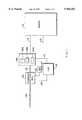
- FIG. 1is a block electrical schematic diagram illustrating the read/write path of a memory of the present invention
- FIG. 2is a diagram illustrating a representative CSR of the present invention.
- FIG. 3is an electrical schematic diagram illustrating filter logic 300 of the present invention.
- the system of the inventionmakes use of a CPU bus 100 that is electrically connected to a command and data register 102 and a CSR 103.
- the command register 102 and the CSR 103are electrically connected by a data and command bus 104.
- the CSR 103includes a plurality of data storage registers (shown in FIG. 2), which in a preferred embodiment comprise memory elements known as "flip-flops".
- Control logic 105is electrically connected to the command and data register 102 via a bus 106; in addition, the control logic 105 is electrically connected to the CSR 103 via a bus 107.
- An error detecting and correcting circuit (EDC) 108is electrically connected to the command register 102 by a bus 110, and is electrically connected to the CSR 103 by a bus 112.
- the EDC 108includes a check bit generator 108a, an error detection circuit 108b, and an error correcting circuit 108c.
- the EDC 108is electrically connected to a memory module 114 via a bus 116.
- the memory module 114comprises several banks of dynamic random access memories (DRAMs).
- DRAMsdynamic random access memories
- “Memory bank”refers to the smallest independently addressable unit of memory, which in a preferred embodiment is about 70 RAM chips.
- the memory module 114is addressable via an address bus 118.
- FIG. 1shows only a single memory module and a single CSR for ease of explanation, it is understood that a computing system utilizing the present invention will typically include multiple CSRs and multiple memory modules.
- each registeris represented by a horizontal row, and corresponds to a single address. In an example of a preferred embodiment, each register contains 31 bits.
- the memory registers 200include an error register 201, a first command trap 202, a second command trap 204, an EDC status register 216, an EDC syndrome register 218, and a filter control register 220.
- an example of filter logic 300 of the inventioncomprises a plurality of digital logic gates including exclusive NOR gates 302-316, AND gates 332, 334, 336, and 338; NAND gate 340, and AND gates 342 and 344.
- Each of the exclusive NOR gates 302-316has one input electrically connected to a different bit of the filter control register 220, with the other input being supplied by the error detecting circuit 108b.
- the outputs of the AND gates 332, 334, 336, and 338are electrically connected to the NAND gate 340.
- the AND gate 342receives input signals from the output of the NAND gate 340, and the error detecting circuit 108b, as described in greater detail below. Inputs to the AND gate 344 are provided by the output of the AND gate 342 and the control logic 105, as described in greater detail below.
- the EDC circuit 108receives a multi-bit data word from the bus 110.
- the data wordcomprises information that the computer (not shown) has placed on the CPU bus 100 for storage in the memory 114.
- the check bit generator 108a of the EDC circuit 108calculates a number of check bits based upon the data word.
- the check bit generator 108acomprises a parity tree arrangement. The calculation of check bits using parity trees is sufficiently well known in the art that an ordinarily skilled artisan, equipped with this specification, would be able to design an arrangement of parity trees suitable for the check bit calculation required for the present invention.
- the data word and its check bitsare stored in the memory 114.
- the error detecting circuit 108breceives from the memory 114 a multi-bit data word and any check bits associated with that data word.
- the error detecting circuit 108bpreferably employs a parity tree arrangement to determine whether the check bits received properly correspond to the data word received.
- the use of parity trees for such an error detecting functionis sufficiently well known in the art that an ordinarily skilled artisan, equipped with this specification, would be able to design an arrangement of parity trees suitable for the present invention.
- the error detecting circuit 108bIf an error is detected, the error detecting circuit 108b generates a syndrome, which is used by the error correcting circuit 108c to correct the error detected by the circuit 108b.
- the syndromeindicates, for example, which bits of the data were found to be erroneous.
- the error detecting circuit 108bidentifies the memory bank in which the read error occurred, and provides a signal identifying that memory bank. Also, the error detecting circuit 108b provides a signal indicating whether the memory error that has been detected is a correctable error or an uncorrectable error.
- the memory registers 200 of the CSR 103function to store various signals each time the memory module 114 experiences an error.
- the signals associated with the new errorare written to certain registers of the CSR 103 in place of the previous contents of such registers.
- the error register 201receives a plurality of signals from various error-indicating circuits (not shown) associated with the memory 114.
- the error register 201contains the parity of the erroneous data, any start or stop bits associated with the data, and the like.
- the first command trap 202is filled with bits 0-31 of the signal that was present on the CPU bus 110 when the error occurred.
- the second command trap 204is filled with bits 32-63 of the signal present on the CPU bus 110 when the error occurred. Bits 32-63 may contain information such as additional data, a command, and a code identifying the processor sending the signal on the CPU bus 100. The contents of the command traps 202 and 204 are obtained from the command and data register 102, which stores each signal sent on the CPU bus 100 for a pre-determined time period.
- the EDC status register 216contains the check bits that were generated by the check bit generator 108a based upon the erroneous data.
- the EDC syndrome register 218contains the syndrome produced by the error detecting circuit 108b in response to the current memory error.
- the filter control register 220is not changed when an error is detected.
- the filter control register 220is set in advance of any error being detected by writing to the CSR 103.
- the bits that are set in the filter control register 220operate to specify a particular error which is to be "filtered” or “masked”.
- the filter logic 300prevents storage of memory errors that correspond to the user-specified characteristics indicated in the register 220.
- the bits of the filter control register 220are designated as shown in Table I, below.
- bits 0-11 of the register 220are used to identify the syndrome of a particular error to be filtered.
- bits 12-13are used to identify the memory bank from which errors should be filtered.
- the operation of the filteris enabled or disabled depending upon the contents of bit 14 (the "enable" bit) of the register 220. To enable the filter, a digital 1 is stored in bit 14; to disable the filter, a digital 0 is stored in bit 14. Therefore, if bit 14 of the register 220 contains a digital 1, the filter logic 300 operates to prevent storage in the CSR 103 of information associated with errors corresponding to the syndrome and memory bank specified in the register 220.
- control logic 105is a state machine that coordinates the operations of the command and data register 102 and the CSR 103.
- the control logic 105provides a write timing signal to the CSR 103, which determines when the CSR 103 is able to store signals associated with errors that occur during the reading or writing of data to the memory 114.
- the control logic 105provides a "CSR write timing signal” that is used to clock the storage of data in the "flip-flops" of the CSR 103.
- control logic 105provides a "CSR read timing signal", which enables the memory 114 to read data onto the bus 116.
- the control logic 105provides an "ACK" signal to acknowledge read and write signals received from the CPU bus 100.
- the filter logic 300performs two basic functions: to determine when a memory error matches the user-selected specifications stored in the register 220, and to prevent storage of information associated with that matching error into the CSR 103.
- the filter logic 300uses the exclusive NOR gates 302-316 to determine whether a memory error matches the user-selected specifications stored in the filter control register 220. Specifically, the exclusive NOR gates 302-314 digitally compare bits 0-11 of the filter control register 220 to the syndrome generated by the error detecting circuit 108b. Similarly, the exclusive NOR gates 315-316 digitally compare bits 12-13 of the filter control register 220 to the memory bank identifying signals provided by the error detecting circuit 108b. If the compared signals are identical, and if bit 14 (the enable bit) of the filter control register 202 has been set to digital 1, the inputs to the AND gates 332, 334, 336, and 338 will all be digital 1. Accordingly, the inputs to the NAND gate 340 will also be equal to digital 1, and the NAND gate 340 will produce a digital 0 at its output.
- the exclusive NOR gates 302-316do not produce a digital 1
- one or more of the AND gates 332, 334, 336, and/or 338will produce a digital 0, which in turn will cause the NAND gate 340 to produce a digital 1.
- the AND gate 342will be allowed to produce a digital 1 if the "correctable error" signal is a digital 1; this will occur if the error is determined to be a correctable error by the error detecting circuit 108b.
- the AND gate 344will be allowed to produce a digital 1 when the "CSR write timing" signal of the control logic 105 is a digital 1, causing the memory registers of the CSR 103 to store information associated with the detected memory error.
- the present inventionprovides a number of advantages over prior arrangements. Specifically, the present invention enables a lesser number of CSRs 103 to be used for each memory module, since the CSR 103 and filter logic 300 may be programmed to selectively prevent data associated with more frequent errors from being stored in the CSR 103. Accordingly, data from less frequent errors is not as likely to be written-over and lost, and the reliability of the computing system is increased. Moreover, the invention does not require any supplemental memory since the existing CSR 103 is utilized, and the invention does not appreciably delay operation of the computing system since operation of the filter logic 300 is rapid.
Landscapes
- Engineering & Computer Science (AREA)
- Theoretical Computer Science (AREA)
- Quality & Reliability (AREA)
- Physics & Mathematics (AREA)
- General Engineering & Computer Science (AREA)
- General Physics & Mathematics (AREA)
- Techniques For Improving Reliability Of Storages (AREA)
Abstract
Description
TABLE I______________________________________FilterControl Register 220______________________________________0 EDC syndrome, bit 01 EDC syndrome, bit 12 EDC syndrome,bit 23 EDC syndrome,bit 34 EDC syndrome,bit 45 EDC syndrome,bit 56 EDC syndrome,bit 67 EDC syndrome,bit 78 EDC syndrome, bit 89 EDC syndrome,bit 910 EDC syndrome, bit 1011 EDC syndrome, bit 1112 Memory Bank, bit 013 Memory Bank, bit 114 Enable______________________________________
Claims (9)
Priority Applications (1)
| Application Number | Priority Date | Filing Date | Title |
|---|---|---|---|
| US08/710,482US5956352A (en) | 1992-04-24 | 1996-09-09 | Adjustable filter for error detecting and correcting system |
Applications Claiming Priority (3)
| Application Number | Priority Date | Filing Date | Title |
|---|---|---|---|
| US87297892A | 1992-04-24 | 1992-04-24 | |
| US39404195A | 1995-02-24 | 1995-02-24 | |
| US08/710,482US5956352A (en) | 1992-04-24 | 1996-09-09 | Adjustable filter for error detecting and correcting system |
Related Parent Applications (1)
| Application Number | Title | Priority Date | Filing Date |
|---|---|---|---|
| US39404195AContinuation | 1992-04-24 | 1995-02-24 |
Publications (1)
| Publication Number | Publication Date |
|---|---|
| US5956352Atrue US5956352A (en) | 1999-09-21 |
Family
ID=27014562
Family Applications (1)
| Application Number | Title | Priority Date | Filing Date |
|---|---|---|---|
| US08/710,482Expired - LifetimeUS5956352A (en) | 1992-04-24 | 1996-09-09 | Adjustable filter for error detecting and correcting system |
Country Status (1)
| Country | Link |
|---|---|
| US (1) | US5956352A (en) |
Cited By (12)
| Publication number | Priority date | Publication date | Assignee | Title |
|---|---|---|---|---|
| US20020166082A1 (en)* | 2001-03-02 | 2002-11-07 | Ramadei Michael J. | System and method for recognizing faults in machines |
| US20030170831A1 (en)* | 1984-12-03 | 2003-09-11 | Fujisawa Pharmaceutical Co. Ltd. | Tricyclo compounds, a process for their production and a pharmaceutical composition containing the same |
| US6728913B1 (en) | 2000-02-25 | 2004-04-27 | Advanced Micro Devices, Inc. | Data recycling in memory |
| US20050283258A1 (en)* | 2004-06-22 | 2005-12-22 | Erwin Thalmann | Method for controlling command sequences, and command control device for carrying out the method |
| WO2008061558A1 (en)* | 2006-11-21 | 2008-05-29 | Freescale Semiconductor, Inc. | Memory system with ecc-unit and further processing arrangement |
| US20090132870A1 (en)* | 2007-11-15 | 2009-05-21 | Inovys Corporation | Dynamic mask memory for serial scan testing |
| US20090150161A1 (en)* | 2004-11-30 | 2009-06-11 | Agere Systems Inc. | Synchronizing parametric coding of spatial audio with externally provided downmix |
| US20110055671A1 (en)* | 2009-09-03 | 2011-03-03 | International Business Machines Corporation | Advanced memory device having improved performance, reduced power and increased reliability |
| WO2013030625A1 (en)* | 2011-08-31 | 2013-03-07 | Freescale Semiconductor, Inc. | Integrated circuit device and method of identifying a presence of a broken connection within an external signal path |
| US20180074734A1 (en)* | 2014-06-11 | 2018-03-15 | International Business Machines Corporation | Bank-level fault management in a memory system |
| US10545824B2 (en) | 2015-06-08 | 2020-01-28 | International Business Machines Corporation | Selective error coding |
| US11010245B2 (en)* | 2018-06-21 | 2021-05-18 | Winbond Electronics Corp. | Memory storage apparatus with dynamic data repair mechanism and method of dynamic data repair thereof |
Citations (10)
| Publication number | Priority date | Publication date | Assignee | Title |
|---|---|---|---|---|
| US3906200A (en)* | 1974-07-05 | 1975-09-16 | Sperry Rand Corp | Error logging in semiconductor storage units |
| US3917933A (en)* | 1974-12-17 | 1975-11-04 | Sperry Rand Corp | Error logging in LSI memory storage units using FIFO memory of LSI shift registers |
| US4535455A (en)* | 1983-03-11 | 1985-08-13 | At&T Bell Laboratories | Correction and monitoring of transient errors in a memory system |
| US4604750A (en)* | 1983-11-07 | 1986-08-05 | Digital Equipment Corporation | Pipeline error correction |
| US4617664A (en)* | 1984-06-29 | 1986-10-14 | International Business Machines Corporation | Error correction for multiple bit output chips |
| US4670880A (en)* | 1984-09-11 | 1987-06-02 | International Business Machines Corp. | Method of error detection and correction by majority |
| US4748627A (en)* | 1985-03-20 | 1988-05-31 | Kabushiki Kaisha Toshiba | Semiconductor memory device with an error correction function |
| US4782486A (en)* | 1987-05-14 | 1988-11-01 | Digital Equipment Corporation | Self-testing memory |
| US4964130A (en)* | 1988-12-21 | 1990-10-16 | Bull Hn Information Systems Inc. | System for determining status of errors in a memory subsystem |
| US5155731A (en)* | 1989-05-11 | 1992-10-13 | Fujitsu Limited | Error logging data storing system |
- 1996
- 1996-09-09USUS08/710,482patent/US5956352A/ennot_activeExpired - Lifetime
Patent Citations (10)
| Publication number | Priority date | Publication date | Assignee | Title |
|---|---|---|---|---|
| US3906200A (en)* | 1974-07-05 | 1975-09-16 | Sperry Rand Corp | Error logging in semiconductor storage units |
| US3917933A (en)* | 1974-12-17 | 1975-11-04 | Sperry Rand Corp | Error logging in LSI memory storage units using FIFO memory of LSI shift registers |
| US4535455A (en)* | 1983-03-11 | 1985-08-13 | At&T Bell Laboratories | Correction and monitoring of transient errors in a memory system |
| US4604750A (en)* | 1983-11-07 | 1986-08-05 | Digital Equipment Corporation | Pipeline error correction |
| US4617664A (en)* | 1984-06-29 | 1986-10-14 | International Business Machines Corporation | Error correction for multiple bit output chips |
| US4670880A (en)* | 1984-09-11 | 1987-06-02 | International Business Machines Corp. | Method of error detection and correction by majority |
| US4748627A (en)* | 1985-03-20 | 1988-05-31 | Kabushiki Kaisha Toshiba | Semiconductor memory device with an error correction function |
| US4782486A (en)* | 1987-05-14 | 1988-11-01 | Digital Equipment Corporation | Self-testing memory |
| US4964130A (en)* | 1988-12-21 | 1990-10-16 | Bull Hn Information Systems Inc. | System for determining status of errors in a memory subsystem |
| US5155731A (en)* | 1989-05-11 | 1992-10-13 | Fujitsu Limited | Error logging data storing system |
Cited By (25)
| Publication number | Priority date | Publication date | Assignee | Title |
|---|---|---|---|---|
| US20030170831A1 (en)* | 1984-12-03 | 2003-09-11 | Fujisawa Pharmaceutical Co. Ltd. | Tricyclo compounds, a process for their production and a pharmaceutical composition containing the same |
| US20030229115A1 (en)* | 1984-12-03 | 2003-12-11 | Fujisawa Pharmaceutical Co., Ltd. | Tricyclo compounds, a process for their production and pharmaceutical composition containing the same |
| US6728913B1 (en) | 2000-02-25 | 2004-04-27 | Advanced Micro Devices, Inc. | Data recycling in memory |
| US6907545B2 (en)* | 2001-03-02 | 2005-06-14 | Pitney Bowes Inc. | System and method for recognizing faults in machines |
| US20020166082A1 (en)* | 2001-03-02 | 2002-11-07 | Ramadei Michael J. | System and method for recognizing faults in machines |
| US20050283258A1 (en)* | 2004-06-22 | 2005-12-22 | Erwin Thalmann | Method for controlling command sequences, and command control device for carrying out the method |
| DE102004030139A1 (en)* | 2004-06-22 | 2006-01-19 | Infineon Technologies Ag | Method for controlling command sequences and command control device for carrying out the method |
| US20090150161A1 (en)* | 2004-11-30 | 2009-06-11 | Agere Systems Inc. | Synchronizing parametric coding of spatial audio with externally provided downmix |
| US8812931B2 (en) | 2006-11-21 | 2014-08-19 | Freescale Semiconductor, Inc. | Memory system with ECC-unit and further processing arrangement |
| US20100058144A1 (en)* | 2006-11-21 | 2010-03-04 | Freescale Semiconductor, Inc | Memory system with ecc-unit and further processing arrangement |
| WO2008061558A1 (en)* | 2006-11-21 | 2008-05-29 | Freescale Semiconductor, Inc. | Memory system with ecc-unit and further processing arrangement |
| US20090132870A1 (en)* | 2007-11-15 | 2009-05-21 | Inovys Corporation | Dynamic mask memory for serial scan testing |
| US7865788B2 (en)* | 2007-11-15 | 2011-01-04 | Verigy (Singapore) Pte. Ltd. | Dynamic mask memory for serial scan testing |
| US20110055671A1 (en)* | 2009-09-03 | 2011-03-03 | International Business Machines Corporation | Advanced memory device having improved performance, reduced power and increased reliability |
| US8307270B2 (en)* | 2009-09-03 | 2012-11-06 | International Business Machines Corporation | Advanced memory device having improved performance, reduced power and increased reliability |
| US8452919B2 (en) | 2009-09-03 | 2013-05-28 | International Business Machines Corporation | Advanced memory device having improved performance, reduced power and increased reliability |
| US8659959B2 (en) | 2009-09-03 | 2014-02-25 | International Business Machines Corporation | Advanced memory device having improved performance, reduced power and increased reliability |
| CN103765580A (en)* | 2011-08-31 | 2014-04-30 | 飞思卡尔半导体公司 | Integrated circuit device and method of identifying a presence of a broken connection within an external signal path |
| WO2013030625A1 (en)* | 2011-08-31 | 2013-03-07 | Freescale Semiconductor, Inc. | Integrated circuit device and method of identifying a presence of a broken connection within an external signal path |
| US9176802B2 (en) | 2011-08-31 | 2015-11-03 | Freescale Semiconductor, Inc. | Integrated circuit device and method of identifying a presence of a broken connection within an external signal path |
| CN103765580B (en)* | 2011-08-31 | 2016-11-16 | 飞思卡尔半导体公司 | There is, in IC apparatus and identification outside signal path, the method disconnected |
| US20180074734A1 (en)* | 2014-06-11 | 2018-03-15 | International Business Machines Corporation | Bank-level fault management in a memory system |
| US10564866B2 (en)* | 2014-06-11 | 2020-02-18 | International Business Machines Corporation | Bank-level fault management in a memory system |
| US10545824B2 (en) | 2015-06-08 | 2020-01-28 | International Business Machines Corporation | Selective error coding |
| US11010245B2 (en)* | 2018-06-21 | 2021-05-18 | Winbond Electronics Corp. | Memory storage apparatus with dynamic data repair mechanism and method of dynamic data repair thereof |
Similar Documents
| Publication | Publication Date | Title |
|---|---|---|
| US4112502A (en) | Conditional bypass of error correction for dual memory access time selection | |
| US6349390B1 (en) | On-board scrubbing of soft errors memory module | |
| US5058115A (en) | Fault tolerant computer memory systems and components employing dual level error correction and detection with lock-up feature | |
| US5228046A (en) | Fault tolerant computer memory systems and components employing dual level error correction and detection with disablement feature | |
| US6065146A (en) | Error correcting memory | |
| US4483003A (en) | Fast parity checking in cache tag memory | |
| US4608687A (en) | Bit steering apparatus and method for correcting errors in stored data, storing the address of the corrected data and using the address to maintain a correct data condition | |
| US4532628A (en) | System for periodically reading all memory locations to detect errors | |
| US3800294A (en) | System for improving the reliability of systems using dirty memories | |
| EP1255197B1 (en) | System and method for correcting soft errors in random access memory devices | |
| AU597140B2 (en) | Efficient address test for large memories | |
| US5379304A (en) | Method and structure for providing error correction code and parity for each byte on SIMM's | |
| US5956352A (en) | Adjustable filter for error detecting and correcting system | |
| US5357521A (en) | Address sensitive memory testing | |
| US5450422A (en) | Method and structure for providing error correction code for each byte on SIMM'S | |
| US5339322A (en) | Cache tag parity detect circuit | |
| EP0386461B1 (en) | Fault tolerant computer memory system with disablement feature | |
| EP0070184B1 (en) | A method of testing memory | |
| JP3130796B2 (en) | Control storage device | |
| JPH05216778A (en) | Memory subsystem | |
| JP3001206B2 (en) | Information processing device | |
| JPS6232826B2 (en) | ||
| JPH02143352A (en) | Memory error detection and correction system | |
| JPS60220444A (en) | Alternate bit control circuit | |
| JPH02144633A (en) | Error correcting device for control storage |
Legal Events
| Date | Code | Title | Description |
|---|---|---|---|
| STCF | Information on status: patent grant | Free format text:PATENTED CASE | |
| FEPP | Fee payment procedure | Free format text:PAYOR NUMBER ASSIGNED (ORIGINAL EVENT CODE: ASPN); ENTITY STATUS OF PATENT OWNER: LARGE ENTITY | |
| AS | Assignment | Owner name:COMPAQ INFORMATION TECHNOLOGIES GROUP, L.P., TEXAS Free format text:ASSIGNMENT OF ASSIGNORS INTEREST;ASSIGNORS:DIGITAL EQUIPMENT CORPORATION;COMPAQ COMPUTER CORPORATION;REEL/FRAME:012447/0903;SIGNING DATES FROM 19991209 TO 20010620 | |
| FPAY | Fee payment | Year of fee payment:4 | |
| AS | Assignment | Owner name:HEWLETT-PACKARD DEVELOPMENT COMPANY, L.P., TEXAS Free format text:CHANGE OF NAME;ASSIGNOR:COMPAQ INFORMANTION TECHNOLOGIES GROUP LP;REEL/FRAME:014102/0224 Effective date:20021001 | |
| FPAY | Fee payment | Year of fee payment:8 | |
| FEPP | Fee payment procedure | Free format text:PAYOR NUMBER ASSIGNED (ORIGINAL EVENT CODE: ASPN); ENTITY STATUS OF PATENT OWNER: LARGE ENTITY Free format text:PAYER NUMBER DE-ASSIGNED (ORIGINAL EVENT CODE: RMPN); ENTITY STATUS OF PATENT OWNER: LARGE ENTITY | |
| FPAY | Fee payment | Year of fee payment:12 |