US5956234A - Method and structure for a surface mountable rigid-flex printed circuit board - Google Patents
Method and structure for a surface mountable rigid-flex printed circuit boardDownload PDFInfo
- Publication number
- US5956234A US5956234AUS09/009,650US965098AUS5956234AUS 5956234 AUS5956234 AUS 5956234AUS 965098 AUS965098 AUS 965098AUS 5956234 AUS5956234 AUS 5956234A
- Authority
- US
- United States
- Prior art keywords
- rigid
- panel
- printed circuit
- circuit board
- flex substrate
- Prior art date
- Legal status (The legal status is an assumption and is not a legal conclusion. Google has not performed a legal analysis and makes no representation as to the accuracy of the status listed.)
- Expired - Lifetime
Links
Images


Classifications
- H—ELECTRICITY
- H05—ELECTRIC TECHNIQUES NOT OTHERWISE PROVIDED FOR
- H05K—PRINTED CIRCUITS; CASINGS OR CONSTRUCTIONAL DETAILS OF ELECTRIC APPARATUS; MANUFACTURE OF ASSEMBLAGES OF ELECTRICAL COMPONENTS
- H05K1/00—Printed circuits
- H05K1/02—Details
- H05K1/14—Structural association of two or more printed circuits
- H05K1/141—One or more single auxiliary printed circuits mounted on a main printed circuit, e.g. modules, adapters
- H—ELECTRICITY
- H05—ELECTRIC TECHNIQUES NOT OTHERWISE PROVIDED FOR
- H05K—PRINTED CIRCUITS; CASINGS OR CONSTRUCTIONAL DETAILS OF ELECTRIC APPARATUS; MANUFACTURE OF ASSEMBLAGES OF ELECTRICAL COMPONENTS
- H05K1/00—Printed circuits
- H05K1/02—Details
- H05K1/14—Structural association of two or more printed circuits
- H05K1/147—Structural association of two or more printed circuits at least one of the printed circuits being bent or folded, e.g. by using a flexible printed circuit
- H—ELECTRICITY
- H05—ELECTRIC TECHNIQUES NOT OTHERWISE PROVIDED FOR
- H05K—PRINTED CIRCUITS; CASINGS OR CONSTRUCTIONAL DETAILS OF ELECTRIC APPARATUS; MANUFACTURE OF ASSEMBLAGES OF ELECTRICAL COMPONENTS
- H05K1/00—Printed circuits
- H05K1/18—Printed circuits structurally associated with non-printed electric components
- H05K1/189—Printed circuits structurally associated with non-printed electric components characterised by the use of a flexible or folded printed circuit
- H—ELECTRICITY
- H05—ELECTRIC TECHNIQUES NOT OTHERWISE PROVIDED FOR
- H05K—PRINTED CIRCUITS; CASINGS OR CONSTRUCTIONAL DETAILS OF ELECTRIC APPARATUS; MANUFACTURE OF ASSEMBLAGES OF ELECTRICAL COMPONENTS
- H05K2201/00—Indexing scheme relating to printed circuits covered by H05K1/00
- H05K2201/10—Details of components or other objects attached to or integrated in a printed circuit board
- H05K2201/10613—Details of electrical connections of non-printed components, e.g. special leads
- H05K2201/10621—Components characterised by their electrical contacts
- H05K2201/10689—Leaded Integrated Circuit [IC] package, e.g. dual-in-line [DIL]
- H—ELECTRICITY
- H05—ELECTRIC TECHNIQUES NOT OTHERWISE PROVIDED FOR
- H05K—PRINTED CIRCUITS; CASINGS OR CONSTRUCTIONAL DETAILS OF ELECTRIC APPARATUS; MANUFACTURE OF ASSEMBLAGES OF ELECTRICAL COMPONENTS
- H05K2201/00—Indexing scheme relating to printed circuits covered by H05K1/00
- H05K2201/10—Details of components or other objects attached to or integrated in a printed circuit board
- H05K2201/10613—Details of electrical connections of non-printed components, e.g. special leads
- H05K2201/10621—Components characterised by their electrical contacts
- H05K2201/10734—Ball grid array [BGA]; Bump grid array
- H—ELECTRICITY
- H05—ELECTRIC TECHNIQUES NOT OTHERWISE PROVIDED FOR
- H05K—PRINTED CIRCUITS; CASINGS OR CONSTRUCTIONAL DETAILS OF ELECTRIC APPARATUS; MANUFACTURE OF ASSEMBLAGES OF ELECTRICAL COMPONENTS
- H05K3/00—Apparatus or processes for manufacturing printed circuits
- H05K3/30—Assembling printed circuits with electric components, e.g. with resistor
- H05K3/32—Assembling printed circuits with electric components, e.g. with resistor electrically connecting electric components or wires to printed circuits
- H05K3/34—Assembling printed circuits with electric components, e.g. with resistor electrically connecting electric components or wires to printed circuits by soldering
- H05K3/341—Surface mounted components
- H05K3/3431—Leadless components
- H05K3/3436—Leadless components having an array of bottom contacts, e.g. pad grid array or ball grid array components
- H—ELECTRICITY
- H05—ELECTRIC TECHNIQUES NOT OTHERWISE PROVIDED FOR
- H05K—PRINTED CIRCUITS; CASINGS OR CONSTRUCTIONAL DETAILS OF ELECTRIC APPARATUS; MANUFACTURE OF ASSEMBLAGES OF ELECTRICAL COMPONENTS
- H05K3/00—Apparatus or processes for manufacturing printed circuits
- H05K3/36—Assembling printed circuits with other printed circuits
- H05K3/361—Assembling flexible printed circuits with other printed circuits
- H05K3/363—Assembling flexible printed circuits with other printed circuits by soldering
- H—ELECTRICITY
- H05—ELECTRIC TECHNIQUES NOT OTHERWISE PROVIDED FOR
- H05K—PRINTED CIRCUITS; CASINGS OR CONSTRUCTIONAL DETAILS OF ELECTRIC APPARATUS; MANUFACTURE OF ASSEMBLAGES OF ELECTRICAL COMPONENTS
- H05K3/00—Apparatus or processes for manufacturing printed circuits
- H05K3/36—Assembling printed circuits with other printed circuits
- H05K3/368—Assembling printed circuits with other printed circuits parallel to each other
- H—ELECTRICITY
- H05—ELECTRIC TECHNIQUES NOT OTHERWISE PROVIDED FOR
- H05K—PRINTED CIRCUITS; CASINGS OR CONSTRUCTIONAL DETAILS OF ELECTRIC APPARATUS; MANUFACTURE OF ASSEMBLAGES OF ELECTRICAL COMPONENTS
- H05K3/00—Apparatus or processes for manufacturing printed circuits
- H05K3/46—Manufacturing multilayer circuits
- H05K3/4688—Composite multilayer circuits, i.e. comprising insulating layers having different properties
- H05K3/4691—Rigid-flexible multilayer circuits comprising rigid and flexible layers, e.g. having in the bending regions only flexible layers
Definitions
- This inventionapplies to semiconductor packaging and mounting.
- multiple chip modules diemay be supplied as either bare untested, unburned-in die or supplied at greater expense as tested, burned in die. If one of the die fails in a multiple chip module using bare die, the entire module may be lost because the replacement procedure may not be cost effective or easy to effect. Hence, it is desirable to use tested, burned-in die. However, using tested burned-in die still does not guarantee that a die in the module will not fail and cause the entire module to be rejected. Therefore, prior art methods for fabricating multiple chip modules are relatively costly.
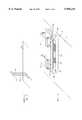
- FIG. 1shows how a rigid-flex board is mounted in the prior art.
- Parallel facing panels 10A and 10Bare conductively and physically connected to each other at their respective upper ends by conductive trace containing tape 12. Together, panels 10A and 10B make up rigid-flex board 10.
- DRAM SIMM connector 15is attached to the bottom edge of panel 10B and conductively and physically connects rigid-flex board 10 to a receptacle (not shown) on printed circuit board 18.
- Rigid-flex board 10is used to allow surface mounting of components on four surfaces: 1) the exterior of panel 10A; 2) the exterior of panel 10B; 3) half of the interior of panel 10A; and 4) the half of the interior of panel 10B opposite the unoccupied half of the interior of panel 10A. This utilizes the area of three out of four panel surfaces while retaining a DRAM SIMM profile.
- the components mounted on rigid-flex board 10may be burned in and tested prior to mounting to ensure operability.
- flexible rigid-flex printed circuit boardscan be configured into three-dimensional multiplanar shapes to provide a high density and volume-efficient form of circuitry.
- a semiconductor packaging structurethat uses packaged components is attached onto a substrate surface with standard surface mount technology (for example, solder screen print or ball grid array).
- Surface mount technologyinvolves electrically and mechanically connecting components to the surface of a conductive pattern (such as on a printed circuit board) without using through holes.
- a rigid-flex printed circuit boardis used as a substrate and converted into a surface mount module, using for example, a ball grid array footprint on one surface of the rigid-flex printed circuit board to provide a package that is surface mountable and has the same density advantages as using bare die in multiple chip modules.
- the end productis testable and reworkable with standard surface mount rework processes whereas bare die in multiple chip modules in most cases are not reworkable as the bare die are permanently sealed in the multiple chip modules.
- the substrate upon which the die(typically silicon whose thermal coefficient differs from the thermal coefficient of the substrate) is mounted is thin, with a thickness selected to be within a desired range, for example between approximately 15-18 mils in some ball grid arrays.
- use of surface mount technology with a rigid-flex boardrequires that the substrate be thicker than in the prior art ball grid array so as to support the packaged semiconductor devices mounted thereon. While the use of a thicker substrate in the rigid-flex board than in the multiple chip module results in a heavier package, a thicker substrate in the rigid-flex board allows the use of more standard technology to mount the packages on the rigid-flex board which lowers tooling requirements and costs.
- Applications of the present inventioninclude allowing economical, space efficient mounting of components in cellular telephones and other portable electronic devices where space is a premium.
- FIG. 1shows prior art mounting of a rigid-flex board on a printed circuit board
- FIG. 2shows an embodiment in accordance with this invention of mounting a rigid-flex board on a printed circuit with surface mount technology
- FIGS. 3A and 3Bshow a top and bottom view, respectively, of one embodiment of the rigid-flex board in accordance with this invention
- FIGS. 4A and 4Bshow the top and bottom interior, respectively, of the rigid-flex board in accordance with an embodiment of this invention
- FIGS. 5A-5Cshow steps in a method of attaching a rigid-flex substrate to a printed circuit board in accordance with one embodiment of this invention
- FIG. 5Dshows a rigid-flex substrate, with a chip, mounted on a printed circuit board by solder screen print surface mount technology.
- surface mount technology and rigid-flex technologyare combined to obtain a semiconductor packaging structure using surface mount technology.
- This inventionallows, for example, a rigid-flex board to be used as a surface mount module.
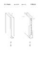
- FIG. 2One embodiment in accordance with this invention is shown in FIG. 2.
- Rigid-flex board 22is shown rotated sideways from the orientation of rigid-flex board 10 in FIG. 1.
- Top panel 27(made in one embodiment of FR-4, fire-retardant epoxy resin-glass cloth laminate) and bottom panel 26 (also made in one embodiment of FR-4) positioned parallel to one another make up rigid-flex board 22.
- Panels 26 and 27(square in one embodiment, but generally of any desired shape) are electrically connected to each other at one edge by conductive-trace-containing tape 29A, such as, for example, Flexcircuit tape.
- Top panel 27is folded over bottom panel 26 in a sandwich configuration with epoxy bead 29B attaching the respective panels to each other on the end opposite to where tape 29A electrically connects panels 26 and 27.
- Rigid-flex board 22is connected to underlying printed circuit board 25 with standard surface mount technology such as ball grid array 25A on the exterior surface of panel 26 in FIG. 2.
- Ball grid array technologiesuse solder balls for mechanical and electrical connection to printed circuit boards.
- Other standard surface mount technologiesthat may be used in accordance with this invention to mount rigid-flex board 22 on printed circuit board 25 are solder screen print technologies. Pin grid array technologies may also be employed to connect rigid-flex board 22 to underlying printed circuit board 25.
- Chip 21is surface mounted on the interior surface of bottom panel 26. To address thermal dissipation concerns, thermoconductive double-sided adhesive tape 28 may be placed on chip 21 as described in commonly assigned U.S. patent application, Ser. No. 08/574,049 which is incorporated herein by reference.
- FIG. 3Bshows a bottom view of panel 26 with ball grid array 25A footprint for surface mounting on corresponding bonding pads (not shown) on printed circuit board 25.
- FIG. 3Ashows a top view of panel 27 with packaged chips 23 and 24 mounted on the top surface of panel 27.
- FIG. 4Bshows a top view of panel 26 with packaged chip 21 mounted thereon and
- FIG. 4Ashows a bottom view of panel 27 with the locations of packaged chips 23 and 24 shown in dashed lines on the top surface of panel 27.
- FIGS. 5A-5Cshow steps in a method of mounting rigid-flex substrate 51 on printed circuit board 55 in accordance with one embodiment of this invention. Specifically, rigid-flex substrate 51 with single mounted chip 52 is shown in FIG. 5C attached to printed circuit board 55 by ball grid array 56 but it is understood that there may be a plurality of components mounted on rigid-flex substrate 51 and rigid-flex substrate 51 may be attached using any surface mount technology to printed circuit board 55.
- An overview of FIGS. 5A-5Cfollows:
- FIG. 5Ashows rigid-flex substrate 51
- FIG. 5Bshows chip 52 mounted on rigid-flex substrate 51
- FIG. 5Cshows rigid-flex substrate 51 with chip 52 mounted on printed circuit board 55.
- FIG. 5Dshows an embodiment of the present invention wherein rigid-flex substrate 51, with chip 52, is mounted on printed circuit board 55 by solder screen print 57.
- a sandwich package in accordance with this inventionis from 250 mils to 350 mils in height depending on the thickness of the packages mounted on the rigid-flex board 22.
- the overall sandwich configurationhas the same footprint as the ball grid array 25A (see FIG. 3B) and allows packaged components that are already burned in and tested to be mounted on rigid-flex board 22.
- rigid-flex board 22as shown in FIGS. 2, 3A, 3B, 4A, and 4B more electrical connections can be made between rigid-flex board 22 and the printed circuit board 25 than with the prior art DRAM SIMM connector style since an entire rigid-flex board panel surface is available for placement of surface mount technology connections.
- the increase in the number of electrical connections that can be made in accordance with this inventionis on the order of the square of the connections available using the prior art DRAM SIMM style connector. This is important since the number of output leads per packaged component is increasing in today's electronics applications. Increasing the number of available electrical connections allows more electronic components to be mounted on rigid-flex board 22 (see FIG. 2).
Landscapes
- Engineering & Computer Science (AREA)
- Microelectronics & Electronic Packaging (AREA)
- Combinations Of Printed Boards (AREA)
Abstract
Description
Claims (15)
Priority Applications (1)
| Application Number | Priority Date | Filing Date | Title |
|---|---|---|---|
| US09/009,650US5956234A (en) | 1998-01-20 | 1998-01-20 | Method and structure for a surface mountable rigid-flex printed circuit board |
Applications Claiming Priority (1)
| Application Number | Priority Date | Filing Date | Title |
|---|---|---|---|
| US09/009,650US5956234A (en) | 1998-01-20 | 1998-01-20 | Method and structure for a surface mountable rigid-flex printed circuit board |
Publications (1)
| Publication Number | Publication Date |
|---|---|
| US5956234Atrue US5956234A (en) | 1999-09-21 |
Family
ID=21738940
Family Applications (1)
| Application Number | Title | Priority Date | Filing Date |
|---|---|---|---|
| US09/009,650Expired - LifetimeUS5956234A (en) | 1998-01-20 | 1998-01-20 | Method and structure for a surface mountable rigid-flex printed circuit board |
Country Status (1)
| Country | Link |
|---|---|
| US (1) | US5956234A (en) |
Cited By (30)
| Publication number | Priority date | Publication date | Assignee | Title |
|---|---|---|---|---|
| US6208521B1 (en)* | 1997-05-19 | 2001-03-27 | Nitto Denko Corporation | Film carrier and laminate type mounting structure using same |
| US20010006252A1 (en)* | 1996-12-13 | 2001-07-05 | Young Kim | Stacked microelectronic assembly and method therefor |
| US6410857B1 (en) | 2001-03-01 | 2002-06-25 | Lockheed Martin Corporation | Signal cross-over interconnect for a double-sided circuit card assembly |
| US6512291B2 (en) | 2001-02-23 | 2003-01-28 | Agere Systems Inc. | Flexible semiconductor device support with integrated thermoelectric cooler and method for making same |
| US20030168725A1 (en)* | 1996-12-13 | 2003-09-11 | Tessera, Inc. | Methods of making microelectronic assemblies including folded substrates |
| US20040099938A1 (en)* | 2002-09-11 | 2004-05-27 | Tessera, Inc. | Assemblies having stacked semiconductor chips and methods of making same |
| US20040104470A1 (en)* | 2002-08-16 | 2004-06-03 | Tessera, Inc. | Microelectronic packages with self-aligning features |
| US6765288B2 (en) | 2002-08-05 | 2004-07-20 | Tessera, Inc. | Microelectronic adaptors, assemblies and methods |
| US20040145054A1 (en)* | 2002-09-06 | 2004-07-29 | Tessera, Inc. | Components, methods and assemblies for stacked packages |
| US20040212063A1 (en)* | 2003-04-28 | 2004-10-28 | Jaeck Edward W. | Electronic package having a flexible substrate with ends connected to one another |
| US20050167817A1 (en)* | 2002-08-05 | 2005-08-04 | Tessera, Inc. | Microelectronic adaptors, assemblies and methods |
| US20070023905A1 (en)* | 2004-03-29 | 2007-02-01 | Intel Corporation | Semiconducting device with folded interposer |
| US7335975B2 (en)* | 2001-10-26 | 2008-02-26 | Staktek Group L.P. | Integrated circuit stacking system and method |
| US20080130234A1 (en)* | 2006-11-30 | 2008-06-05 | Daisuke Maehara | Electronic Apparatus |
| US7656678B2 (en) | 2001-10-26 | 2010-02-02 | Entorian Technologies, Lp | Stacked module systems |
| US20100193970A1 (en)* | 2003-12-30 | 2010-08-05 | Tessera, Inc. | Micro pin grid array with pin motion isolation |
| CN103200789A (en)* | 2013-03-18 | 2013-07-10 | 昆山汇仁氏电子有限公司 | Printed circuit board transplanting technology |
| US8580607B2 (en) | 2010-07-27 | 2013-11-12 | Tessera, Inc. | Microelectronic packages with nanoparticle joining |
| US8604348B2 (en) | 2003-10-06 | 2013-12-10 | Tessera, Inc. | Method of making a connection component with posts and pads |
| US8641913B2 (en) | 2003-10-06 | 2014-02-04 | Tessera, Inc. | Fine pitch microcontacts and method for forming thereof |
| US8723318B2 (en) | 2010-07-08 | 2014-05-13 | Tessera, Inc. | Microelectronic packages with dual or multiple-etched flip-chip connectors |
| US8853558B2 (en) | 2010-12-10 | 2014-10-07 | Tessera, Inc. | Interconnect structure |
| US8884448B2 (en) | 2007-09-28 | 2014-11-11 | Tessera, Inc. | Flip chip interconnection with double post |
| US9325075B1 (en) | 2012-05-25 | 2016-04-26 | Lockheed Martin Corporation | Antennae formed using integrated subarrays |
| US9633971B2 (en) | 2015-07-10 | 2017-04-25 | Invensas Corporation | Structures and methods for low temperature bonding using nanoparticles |
| US10231337B2 (en)* | 2014-12-16 | 2019-03-12 | Inertial Sense, Inc. | Folded printed circuit assemblies and related methods |
| JP2019145765A (en)* | 2018-02-19 | 2019-08-29 | サムソン エレクトロ−メカニックス カンパニーリミテッド. | Printed circuit board |
| US10535626B2 (en) | 2015-07-10 | 2020-01-14 | Invensas Corporation | Structures and methods for low temperature bonding using nanoparticles |
| US11973056B2 (en) | 2016-10-27 | 2024-04-30 | Adeia Semiconductor Technologies Llc | Methods for low temperature bonding using nanoparticles |
| US12211809B2 (en) | 2020-12-30 | 2025-01-28 | Adeia Semiconductor Bonding Technologies Inc. | Structure with conductive feature and method of forming same |
Citations (15)
| Publication number | Priority date | Publication date | Assignee | Title |
|---|---|---|---|---|
| US4956694A (en)* | 1988-11-04 | 1990-09-11 | Dense-Pac Microsystems, Inc. | Integrated circuit chip stacking |
| US5161009A (en)* | 1990-06-07 | 1992-11-03 | Casio Computer Co., Ltd. | Ic module having a folding junction structure |
| US5224023A (en)* | 1992-02-10 | 1993-06-29 | Smith Gary W | Foldable electronic assembly module |
| US5280193A (en)* | 1992-05-04 | 1994-01-18 | Lin Paul T | Repairable semiconductor multi-package module having individualized package bodies on a PC board substrate |
| US5295838A (en)* | 1993-01-14 | 1994-03-22 | Hughes Aircraft Company | Raised feature/gold dot pressure interconnections of rigid-flex circuits and rigid circuit boards |
| US5309326A (en)* | 1991-12-06 | 1994-05-03 | Rohm Co., Ltd. | Circuit module having stacked circuit boards |
| US5311402A (en)* | 1992-02-14 | 1994-05-10 | Nec Corporation | Semiconductor device package having locating mechanism for properly positioning semiconductor device within package |
| US5313096A (en)* | 1992-03-16 | 1994-05-17 | Dense-Pac Microsystems, Inc. | IC chip package having chip attached to and wire bonded within an overlying substrate |
| US5386341A (en)* | 1993-11-01 | 1995-01-31 | Motorola, Inc. | Flexible substrate folded in a U-shape with a rigidizer plate located in the notch of the U-shape |
| US5428190A (en)* | 1993-07-02 | 1995-06-27 | Sheldahl, Inc. | Rigid-flex board with anisotropic interconnect and method of manufacture |
| US5448511A (en)* | 1994-06-01 | 1995-09-05 | Storage Technology Corporation | Memory stack with an integrated interconnect and mounting structure |
| US5459287A (en)* | 1994-05-18 | 1995-10-17 | Dell Usa, L.P. | Socketed printed circuit board BGA connection apparatus and associated methods |
| US5490324A (en)* | 1993-09-15 | 1996-02-13 | Lsi Logic Corporation | Method of making integrated circuit package having multiple bonding tiers |
| US5717556A (en)* | 1995-04-26 | 1998-02-10 | Nec Corporation | Printed-wiring board having plural parallel-connected interconnections |
| US5822191A (en)* | 1994-08-04 | 1998-10-13 | Sharp Kabushiki Kaisha | Integrated circuit mounting tape |
- 1998
- 1998-01-20USUS09/009,650patent/US5956234A/ennot_activeExpired - Lifetime
Patent Citations (15)
| Publication number | Priority date | Publication date | Assignee | Title |
|---|---|---|---|---|
| US4956694A (en)* | 1988-11-04 | 1990-09-11 | Dense-Pac Microsystems, Inc. | Integrated circuit chip stacking |
| US5161009A (en)* | 1990-06-07 | 1992-11-03 | Casio Computer Co., Ltd. | Ic module having a folding junction structure |
| US5309326A (en)* | 1991-12-06 | 1994-05-03 | Rohm Co., Ltd. | Circuit module having stacked circuit boards |
| US5224023A (en)* | 1992-02-10 | 1993-06-29 | Smith Gary W | Foldable electronic assembly module |
| US5311402A (en)* | 1992-02-14 | 1994-05-10 | Nec Corporation | Semiconductor device package having locating mechanism for properly positioning semiconductor device within package |
| US5313096A (en)* | 1992-03-16 | 1994-05-17 | Dense-Pac Microsystems, Inc. | IC chip package having chip attached to and wire bonded within an overlying substrate |
| US5280193A (en)* | 1992-05-04 | 1994-01-18 | Lin Paul T | Repairable semiconductor multi-package module having individualized package bodies on a PC board substrate |
| US5295838A (en)* | 1993-01-14 | 1994-03-22 | Hughes Aircraft Company | Raised feature/gold dot pressure interconnections of rigid-flex circuits and rigid circuit boards |
| US5428190A (en)* | 1993-07-02 | 1995-06-27 | Sheldahl, Inc. | Rigid-flex board with anisotropic interconnect and method of manufacture |
| US5490324A (en)* | 1993-09-15 | 1996-02-13 | Lsi Logic Corporation | Method of making integrated circuit package having multiple bonding tiers |
| US5386341A (en)* | 1993-11-01 | 1995-01-31 | Motorola, Inc. | Flexible substrate folded in a U-shape with a rigidizer plate located in the notch of the U-shape |
| US5459287A (en)* | 1994-05-18 | 1995-10-17 | Dell Usa, L.P. | Socketed printed circuit board BGA connection apparatus and associated methods |
| US5448511A (en)* | 1994-06-01 | 1995-09-05 | Storage Technology Corporation | Memory stack with an integrated interconnect and mounting structure |
| US5822191A (en)* | 1994-08-04 | 1998-10-13 | Sharp Kabushiki Kaisha | Integrated circuit mounting tape |
| US5717556A (en)* | 1995-04-26 | 1998-02-10 | Nec Corporation | Printed-wiring board having plural parallel-connected interconnections |
Non-Patent Citations (6)
| Title |
|---|
| Advertorial, "New Test Demands for Chip-to-Chip Interconnect", Electronic Packaging & Production (1 page). |
| Advertorial, New Test Demands for Chip to Chip Interconnect , Electronic Packaging & Production (1 page).* |
| Gilleo, "A Simplified Version of the Multilayer Circuit Process", Electronic Packaging & Production, Feb. 1989 (4 pages). |
| Gilleo, A Simplified Version of the Multilayer Circuit Process , Electronic Packaging & Production, Feb. 1989 (4 pages).* |
| Markstein, "Rigid-Flex: a Maturing Technology", Electronic Packaging & Production, Feb. 1996 (7 pages). |
| Markstein, Rigid Flex: a Maturing Technology , Electronic Packaging & Production, Feb. 1996 (7 pages).* |
Cited By (52)
| Publication number | Priority date | Publication date | Assignee | Title |
|---|---|---|---|---|
| US7149095B2 (en) | 1996-12-13 | 2006-12-12 | Tessera, Inc. | Stacked microelectronic assemblies |
| US20010006252A1 (en)* | 1996-12-13 | 2001-07-05 | Young Kim | Stacked microelectronic assembly and method therefor |
| US20030168725A1 (en)* | 1996-12-13 | 2003-09-11 | Tessera, Inc. | Methods of making microelectronic assemblies including folded substrates |
| US6699730B2 (en) | 1996-12-13 | 2004-03-02 | Tessers, Inc. | Stacked microelectronic assembly and method therefor |
| US6208521B1 (en)* | 1997-05-19 | 2001-03-27 | Nitto Denko Corporation | Film carrier and laminate type mounting structure using same |
| US6512291B2 (en) | 2001-02-23 | 2003-01-28 | Agere Systems Inc. | Flexible semiconductor device support with integrated thermoelectric cooler and method for making same |
| US6410857B1 (en) | 2001-03-01 | 2002-06-25 | Lockheed Martin Corporation | Signal cross-over interconnect for a double-sided circuit card assembly |
| US7606048B2 (en)* | 2001-10-26 | 2009-10-20 | Enthorian Technologies, LP | Integrated circuit stacking system |
| US7656678B2 (en) | 2001-10-26 | 2010-02-02 | Entorian Technologies, Lp | Stacked module systems |
| US7335975B2 (en)* | 2001-10-26 | 2008-02-26 | Staktek Group L.P. | Integrated circuit stacking system and method |
| US6765288B2 (en) | 2002-08-05 | 2004-07-20 | Tessera, Inc. | Microelectronic adaptors, assemblies and methods |
| US20040217461A1 (en)* | 2002-08-05 | 2004-11-04 | Tessera, Inc. | Microelectronic adaptors, assemblies and methods |
| US20050167817A1 (en)* | 2002-08-05 | 2005-08-04 | Tessera, Inc. | Microelectronic adaptors, assemblies and methods |
| US7053485B2 (en) | 2002-08-16 | 2006-05-30 | Tessera, Inc. | Microelectronic packages with self-aligning features |
| US20040104470A1 (en)* | 2002-08-16 | 2004-06-03 | Tessera, Inc. | Microelectronic packages with self-aligning features |
| US20040145054A1 (en)* | 2002-09-06 | 2004-07-29 | Tessera, Inc. | Components, methods and assemblies for stacked packages |
| US20080042274A1 (en)* | 2002-09-06 | 2008-02-21 | Tessera, Inc. | Components, methods and assemblies for stacked packages |
| US7935569B2 (en) | 2002-09-06 | 2011-05-03 | Tessera, Inc. | Components, methods and assemblies for stacked packages |
| US7294928B2 (en) | 2002-09-06 | 2007-11-13 | Tessera, Inc. | Components, methods and assemblies for stacked packages |
| US20040099938A1 (en)* | 2002-09-11 | 2004-05-27 | Tessera, Inc. | Assemblies having stacked semiconductor chips and methods of making same |
| US7071547B2 (en) | 2002-09-11 | 2006-07-04 | Tessera, Inc. | Assemblies having stacked semiconductor chips and methods of making same |
| US6841855B2 (en)* | 2003-04-28 | 2005-01-11 | Intel Corporation | Electronic package having a flexible substrate with ends connected to one another |
| US20040212063A1 (en)* | 2003-04-28 | 2004-10-28 | Jaeck Edward W. | Electronic package having a flexible substrate with ends connected to one another |
| US8641913B2 (en) | 2003-10-06 | 2014-02-04 | Tessera, Inc. | Fine pitch microcontacts and method for forming thereof |
| US8604348B2 (en) | 2003-10-06 | 2013-12-10 | Tessera, Inc. | Method of making a connection component with posts and pads |
| US20100193970A1 (en)* | 2003-12-30 | 2010-08-05 | Tessera, Inc. | Micro pin grid array with pin motion isolation |
| US8531039B2 (en) | 2003-12-30 | 2013-09-10 | Tessera, Inc. | Micro pin grid array with pin motion isolation |
| US7482698B2 (en)* | 2004-03-29 | 2009-01-27 | Intel Corporation | Semiconducting device with folded interposer |
| US20070023905A1 (en)* | 2004-03-29 | 2007-02-01 | Intel Corporation | Semiconducting device with folded interposer |
| US20080130234A1 (en)* | 2006-11-30 | 2008-06-05 | Daisuke Maehara | Electronic Apparatus |
| US8884448B2 (en) | 2007-09-28 | 2014-11-11 | Tessera, Inc. | Flip chip interconnection with double post |
| US8723318B2 (en) | 2010-07-08 | 2014-05-13 | Tessera, Inc. | Microelectronic packages with dual or multiple-etched flip-chip connectors |
| US9030001B2 (en) | 2010-07-27 | 2015-05-12 | Tessera, Inc. | Microelectronic packages with nanoparticle joining |
| US8580607B2 (en) | 2010-07-27 | 2013-11-12 | Tessera, Inc. | Microelectronic packages with nanoparticle joining |
| US9397063B2 (en) | 2010-07-27 | 2016-07-19 | Tessera, Inc. | Microelectronic packages with nanoparticle joining |
| US9496236B2 (en) | 2010-12-10 | 2016-11-15 | Tessera, Inc. | Interconnect structure |
| US8853558B2 (en) | 2010-12-10 | 2014-10-07 | Tessera, Inc. | Interconnect structure |
| US9325075B1 (en) | 2012-05-25 | 2016-04-26 | Lockheed Martin Corporation | Antennae formed using integrated subarrays |
| CN103200789A (en)* | 2013-03-18 | 2013-07-10 | 昆山汇仁氏电子有限公司 | Printed circuit board transplanting technology |
| CN103200789B (en)* | 2013-03-18 | 2017-06-16 | 昆山汇仁氏电子有限公司 | A kind of printed wiring board transplanting technique |
| US10231337B2 (en)* | 2014-12-16 | 2019-03-12 | Inertial Sense, Inc. | Folded printed circuit assemblies and related methods |
| US10535626B2 (en) | 2015-07-10 | 2020-01-14 | Invensas Corporation | Structures and methods for low temperature bonding using nanoparticles |
| US9818713B2 (en) | 2015-07-10 | 2017-11-14 | Invensas Corporation | Structures and methods for low temperature bonding using nanoparticles |
| US9633971B2 (en) | 2015-07-10 | 2017-04-25 | Invensas Corporation | Structures and methods for low temperature bonding using nanoparticles |
| US10886250B2 (en) | 2015-07-10 | 2021-01-05 | Invensas Corporation | Structures and methods for low temperature bonding using nanoparticles |
| US10892246B2 (en) | 2015-07-10 | 2021-01-12 | Invensas Corporation | Structures and methods for low temperature bonding using nanoparticles |
| US11710718B2 (en) | 2015-07-10 | 2023-07-25 | Adeia Semiconductor Technologies Llc | Structures and methods for low temperature bonding using nanoparticles |
| US11973056B2 (en) | 2016-10-27 | 2024-04-30 | Adeia Semiconductor Technologies Llc | Methods for low temperature bonding using nanoparticles |
| US12027487B2 (en) | 2016-10-27 | 2024-07-02 | Adeia Semiconductor Technologies Llc | Structures for low temperature bonding using nanoparticles |
| JP2019145765A (en)* | 2018-02-19 | 2019-08-29 | サムソン エレクトロ−メカニックス カンパニーリミテッド. | Printed circuit board |
| JP7206474B2 (en) | 2018-02-19 | 2023-01-18 | サムソン エレクトロ-メカニックス カンパニーリミテッド. | printed circuit board |
| US12211809B2 (en) | 2020-12-30 | 2025-01-28 | Adeia Semiconductor Bonding Technologies Inc. | Structure with conductive feature and method of forming same |
Similar Documents
| Publication | Publication Date | Title |
|---|---|---|
| US5956234A (en) | Method and structure for a surface mountable rigid-flex printed circuit board | |
| US5724230A (en) | Flexible laminate module including spacers embedded in an adhesive | |
| US6900529B2 (en) | Electronic module having a three dimensional array of carrier-mounted integrated circuit packages | |
| US4730232A (en) | High density microelectronic packaging module for high speed chips | |
| US6919626B2 (en) | High density integrated circuit module | |
| US7405471B2 (en) | Carrier-based electronic module | |
| JP2570498B2 (en) | Integrated circuit chip carrier | |
| US5027191A (en) | Cavity-down chip carrier with pad grid array | |
| US6522018B1 (en) | Ball grid array chip packages having improved testing and stacking characteristics | |
| US5620928A (en) | Ultra thin ball grid array using a flex tape or printed wiring board substrate and method | |
| US5065280A (en) | Flex interconnect module | |
| US6313998B1 (en) | Circuit board assembly having a three dimensional array of integrated circuit packages | |
| US6545868B1 (en) | Electronic module having canopy-type carriers | |
| US20050139980A1 (en) | High density integrated circuit module | |
| US20060209515A1 (en) | Processor/memory module with foldable substrate | |
| US9070566B2 (en) | High density composite focal plane array | |
| US6469903B1 (en) | Flexible printed circuit and semiconductor device | |
| US20030043650A1 (en) | Multilayered memory device | |
| US5699228A (en) | Method of interconnecting leadless devices to printed wiring boards and apparatus produced thereby | |
| US6744128B2 (en) | Integrated circuit package capable of improving signal quality | |
| JP4016587B2 (en) | Electronic component and manufacturing method thereof | |
| JP2705468B2 (en) | Hybrid integrated circuit device | |
| KR0163868B1 (en) | Down set pcb and mounting module | |
| US20040042189A1 (en) | Multi-chip integrated module | |
| JP2007173486A (en) | Small multi-chip module and manufacturing method therefor |
Legal Events
| Date | Code | Title | Description |
|---|---|---|---|
| AS | Assignment | Owner name:INTEGRATED DEVICE TECHNOLOGY, INC., CALIFORNIA Free format text:ASSIGNMENT OF ASSIGNORS INTEREST;ASSIGNOR:MUELLER, GERHARD M.;REEL/FRAME:008936/0420 Effective date:19970915 | |
| STCF | Information on status: patent grant | Free format text:PATENTED CASE | |
| FPAY | Fee payment | Year of fee payment:4 | |
| REMI | Maintenance fee reminder mailed | ||
| FPAY | Fee payment | Year of fee payment:8 | |
| FPAY | Fee payment | Year of fee payment:12 | |
| AS | Assignment | Owner name:JPMORGAN CHASE BANK, N.A., AS COLLATERAL AGENT, NE Free format text:SECURITY AGREEMENT;ASSIGNORS:INTEGRATED DEVICE TECHNOLOGY, INC.;GIGPEAK, INC.;MAGNUM SEMICONDUCTOR, INC.;AND OTHERS;REEL/FRAME:042166/0431 Effective date:20170404 Owner name:JPMORGAN CHASE BANK, N.A., AS COLLATERAL AGENT, NEW YORK Free format text:SECURITY AGREEMENT;ASSIGNORS:INTEGRATED DEVICE TECHNOLOGY, INC.;GIGPEAK, INC.;MAGNUM SEMICONDUCTOR, INC.;AND OTHERS;REEL/FRAME:042166/0431 Effective date:20170404 | |
| AS | Assignment | Owner name:CHIPX, INCORPORATED, CALIFORNIA Free format text:RELEASE BY SECURED PARTY;ASSIGNOR:JPMORGAN CHASE BANK, N.A.;REEL/FRAME:048746/0001 Effective date:20190329 Owner name:GIGPEAK, INC., CALIFORNIA Free format text:RELEASE BY SECURED PARTY;ASSIGNOR:JPMORGAN CHASE BANK, N.A.;REEL/FRAME:048746/0001 Effective date:20190329 Owner name:INTEGRATED DEVICE TECHNOLOGY, INC., CALIFORNIA Free format text:RELEASE BY SECURED PARTY;ASSIGNOR:JPMORGAN CHASE BANK, N.A.;REEL/FRAME:048746/0001 Effective date:20190329 Owner name:ENDWAVE CORPORATION, CALIFORNIA Free format text:RELEASE BY SECURED PARTY;ASSIGNOR:JPMORGAN CHASE BANK, N.A.;REEL/FRAME:048746/0001 Effective date:20190329 Owner name:MAGNUM SEMICONDUCTOR, INC., CALIFORNIA Free format text:RELEASE BY SECURED PARTY;ASSIGNOR:JPMORGAN CHASE BANK, N.A.;REEL/FRAME:048746/0001 Effective date:20190329 |