US5956014A - Brightness control and power control of display device - Google Patents
Brightness control and power control of display deviceDownload PDFInfo
- Publication number
- US5956014A US5956014AUS08/544,590US54459095AUS5956014AUS 5956014 AUS5956014 AUS 5956014AUS 54459095 AUS54459095 AUS 54459095AUS 5956014 AUS5956014 AUS 5956014A
- Authority
- US
- United States
- Prior art keywords
- value
- brightness
- brightness value
- display
- power consumption
- Prior art date
- Legal status (The legal status is an assumption and is not a legal conclusion. Google has not performed a legal analysis and makes no representation as to the accuracy of the status listed.)
- Expired - Lifetime
Links
Images


Classifications
- G—PHYSICS
- G09—EDUCATION; CRYPTOGRAPHY; DISPLAY; ADVERTISING; SEALS
- G09G—ARRANGEMENTS OR CIRCUITS FOR CONTROL OF INDICATING DEVICES USING STATIC MEANS TO PRESENT VARIABLE INFORMATION
- G09G3/00—Control arrangements or circuits, of interest only in connection with visual indicators other than cathode-ray tubes
- G09G3/20—Control arrangements or circuits, of interest only in connection with visual indicators other than cathode-ray tubes for presentation of an assembly of a number of characters, e.g. a page, by composing the assembly by combination of individual elements arranged in a matrix no fixed position being assigned to or needed to be assigned to the individual characters or partial characters
- G09G3/22—Control arrangements or circuits, of interest only in connection with visual indicators other than cathode-ray tubes for presentation of an assembly of a number of characters, e.g. a page, by composing the assembly by combination of individual elements arranged in a matrix no fixed position being assigned to or needed to be assigned to the individual characters or partial characters using controlled light sources
- G09G3/28—Control arrangements or circuits, of interest only in connection with visual indicators other than cathode-ray tubes for presentation of an assembly of a number of characters, e.g. a page, by composing the assembly by combination of individual elements arranged in a matrix no fixed position being assigned to or needed to be assigned to the individual characters or partial characters using controlled light sources using luminous gas-discharge panels, e.g. plasma panels
- G09G3/288—Control arrangements or circuits, of interest only in connection with visual indicators other than cathode-ray tubes for presentation of an assembly of a number of characters, e.g. a page, by composing the assembly by combination of individual elements arranged in a matrix no fixed position being assigned to or needed to be assigned to the individual characters or partial characters using controlled light sources using luminous gas-discharge panels, e.g. plasma panels using AC panels
- G09G3/296—Driving circuits for producing the waveforms applied to the driving electrodes
- G—PHYSICS
- G09—EDUCATION; CRYPTOGRAPHY; DISPLAY; ADVERTISING; SEALS
- G09G—ARRANGEMENTS OR CIRCUITS FOR CONTROL OF INDICATING DEVICES USING STATIC MEANS TO PRESENT VARIABLE INFORMATION
- G09G3/00—Control arrangements or circuits, of interest only in connection with visual indicators other than cathode-ray tubes
- G09G3/20—Control arrangements or circuits, of interest only in connection with visual indicators other than cathode-ray tubes for presentation of an assembly of a number of characters, e.g. a page, by composing the assembly by combination of individual elements arranged in a matrix no fixed position being assigned to or needed to be assigned to the individual characters or partial characters
- G09G3/22—Control arrangements or circuits, of interest only in connection with visual indicators other than cathode-ray tubes for presentation of an assembly of a number of characters, e.g. a page, by composing the assembly by combination of individual elements arranged in a matrix no fixed position being assigned to or needed to be assigned to the individual characters or partial characters using controlled light sources
- G09G3/28—Control arrangements or circuits, of interest only in connection with visual indicators other than cathode-ray tubes for presentation of an assembly of a number of characters, e.g. a page, by composing the assembly by combination of individual elements arranged in a matrix no fixed position being assigned to or needed to be assigned to the individual characters or partial characters using controlled light sources using luminous gas-discharge panels, e.g. plasma panels
- G09G3/288—Control arrangements or circuits, of interest only in connection with visual indicators other than cathode-ray tubes for presentation of an assembly of a number of characters, e.g. a page, by composing the assembly by combination of individual elements arranged in a matrix no fixed position being assigned to or needed to be assigned to the individual characters or partial characters using controlled light sources using luminous gas-discharge panels, e.g. plasma panels using AC panels
- G09G3/297—Control arrangements or circuits, of interest only in connection with visual indicators other than cathode-ray tubes for presentation of an assembly of a number of characters, e.g. a page, by composing the assembly by combination of individual elements arranged in a matrix no fixed position being assigned to or needed to be assigned to the individual characters or partial characters using controlled light sources using luminous gas-discharge panels, e.g. plasma panels using AC panels using opposed discharge type panels
- G—PHYSICS
- G09—EDUCATION; CRYPTOGRAPHY; DISPLAY; ADVERTISING; SEALS
- G09G—ARRANGEMENTS OR CIRCUITS FOR CONTROL OF INDICATING DEVICES USING STATIC MEANS TO PRESENT VARIABLE INFORMATION
- G09G2320/00—Control of display operating conditions
- G09G2320/04—Maintaining the quality of display appearance
- G09G2320/043—Preventing or counteracting the effects of ageing
- G—PHYSICS
- G09—EDUCATION; CRYPTOGRAPHY; DISPLAY; ADVERTISING; SEALS
- G09G—ARRANGEMENTS OR CIRCUITS FOR CONTROL OF INDICATING DEVICES USING STATIC MEANS TO PRESENT VARIABLE INFORMATION
- G09G2320/00—Control of display operating conditions
- G09G2320/06—Adjustment of display parameters
- G09G2320/0606—Manual adjustment
- G—PHYSICS
- G09—EDUCATION; CRYPTOGRAPHY; DISPLAY; ADVERTISING; SEALS
- G09G—ARRANGEMENTS OR CIRCUITS FOR CONTROL OF INDICATING DEVICES USING STATIC MEANS TO PRESENT VARIABLE INFORMATION
- G09G2320/00—Control of display operating conditions
- G09G2320/06—Adjustment of display parameters
- G09G2320/0626—Adjustment of display parameters for control of overall brightness
- G—PHYSICS
- G09—EDUCATION; CRYPTOGRAPHY; DISPLAY; ADVERTISING; SEALS
- G09G—ARRANGEMENTS OR CIRCUITS FOR CONTROL OF INDICATING DEVICES USING STATIC MEANS TO PRESENT VARIABLE INFORMATION
- G09G2330/00—Aspects of power supply; Aspects of display protection and defect management
- G09G2330/02—Details of power systems and of start or stop of display operation
- G09G2330/021—Power management, e.g. power saving
- G—PHYSICS
- G09—EDUCATION; CRYPTOGRAPHY; DISPLAY; ADVERTISING; SEALS
- G09G—ARRANGEMENTS OR CIRCUITS FOR CONTROL OF INDICATING DEVICES USING STATIC MEANS TO PRESENT VARIABLE INFORMATION
- G09G2330/00—Aspects of power supply; Aspects of display protection and defect management
- G09G2330/04—Display protection
- G09G2330/045—Protection against panel overheating
- G—PHYSICS
- G09—EDUCATION; CRYPTOGRAPHY; DISPLAY; ADVERTISING; SEALS
- G09G—ARRANGEMENTS OR CIRCUITS FOR CONTROL OF INDICATING DEVICES USING STATIC MEANS TO PRESENT VARIABLE INFORMATION
- G09G3/00—Control arrangements or circuits, of interest only in connection with visual indicators other than cathode-ray tubes
- G09G3/20—Control arrangements or circuits, of interest only in connection with visual indicators other than cathode-ray tubes for presentation of an assembly of a number of characters, e.g. a page, by composing the assembly by combination of individual elements arranged in a matrix no fixed position being assigned to or needed to be assigned to the individual characters or partial characters
- G09G3/22—Control arrangements or circuits, of interest only in connection with visual indicators other than cathode-ray tubes for presentation of an assembly of a number of characters, e.g. a page, by composing the assembly by combination of individual elements arranged in a matrix no fixed position being assigned to or needed to be assigned to the individual characters or partial characters using controlled light sources
- G09G3/28—Control arrangements or circuits, of interest only in connection with visual indicators other than cathode-ray tubes for presentation of an assembly of a number of characters, e.g. a page, by composing the assembly by combination of individual elements arranged in a matrix no fixed position being assigned to or needed to be assigned to the individual characters or partial characters using controlled light sources using luminous gas-discharge panels, e.g. plasma panels
- G09G3/288—Control arrangements or circuits, of interest only in connection with visual indicators other than cathode-ray tubes for presentation of an assembly of a number of characters, e.g. a page, by composing the assembly by combination of individual elements arranged in a matrix no fixed position being assigned to or needed to be assigned to the individual characters or partial characters using controlled light sources using luminous gas-discharge panels, e.g. plasma panels using AC panels
- G09G3/291—Control arrangements or circuits, of interest only in connection with visual indicators other than cathode-ray tubes for presentation of an assembly of a number of characters, e.g. a page, by composing the assembly by combination of individual elements arranged in a matrix no fixed position being assigned to or needed to be assigned to the individual characters or partial characters using controlled light sources using luminous gas-discharge panels, e.g. plasma panels using AC panels controlling the gas discharge to control a cell condition, e.g. by means of specific pulse shapes
- G09G3/293—Control arrangements or circuits, of interest only in connection with visual indicators other than cathode-ray tubes for presentation of an assembly of a number of characters, e.g. a page, by composing the assembly by combination of individual elements arranged in a matrix no fixed position being assigned to or needed to be assigned to the individual characters or partial characters using controlled light sources using luminous gas-discharge panels, e.g. plasma panels using AC panels controlling the gas discharge to control a cell condition, e.g. by means of specific pulse shapes for address discharge
- G—PHYSICS
- G09—EDUCATION; CRYPTOGRAPHY; DISPLAY; ADVERTISING; SEALS
- G09G—ARRANGEMENTS OR CIRCUITS FOR CONTROL OF INDICATING DEVICES USING STATIC MEANS TO PRESENT VARIABLE INFORMATION
- G09G3/00—Control arrangements or circuits, of interest only in connection with visual indicators other than cathode-ray tubes
- G09G3/20—Control arrangements or circuits, of interest only in connection with visual indicators other than cathode-ray tubes for presentation of an assembly of a number of characters, e.g. a page, by composing the assembly by combination of individual elements arranged in a matrix no fixed position being assigned to or needed to be assigned to the individual characters or partial characters
- G09G3/22—Control arrangements or circuits, of interest only in connection with visual indicators other than cathode-ray tubes for presentation of an assembly of a number of characters, e.g. a page, by composing the assembly by combination of individual elements arranged in a matrix no fixed position being assigned to or needed to be assigned to the individual characters or partial characters using controlled light sources
- G09G3/28—Control arrangements or circuits, of interest only in connection with visual indicators other than cathode-ray tubes for presentation of an assembly of a number of characters, e.g. a page, by composing the assembly by combination of individual elements arranged in a matrix no fixed position being assigned to or needed to be assigned to the individual characters or partial characters using controlled light sources using luminous gas-discharge panels, e.g. plasma panels
- G09G3/288—Control arrangements or circuits, of interest only in connection with visual indicators other than cathode-ray tubes for presentation of an assembly of a number of characters, e.g. a page, by composing the assembly by combination of individual elements arranged in a matrix no fixed position being assigned to or needed to be assigned to the individual characters or partial characters using controlled light sources using luminous gas-discharge panels, e.g. plasma panels using AC panels
- G09G3/298—Control arrangements or circuits, of interest only in connection with visual indicators other than cathode-ray tubes for presentation of an assembly of a number of characters, e.g. a page, by composing the assembly by combination of individual elements arranged in a matrix no fixed position being assigned to or needed to be assigned to the individual characters or partial characters using controlled light sources using luminous gas-discharge panels, e.g. plasma panels using AC panels using surface discharge panels
Definitions
- the present inventionrelates to control of a display device and, more particularly, to brightness control and power control of a plasma display panel (PDP).
- PDPplasma display panel
- a variety of brightness controllershave heretofore been provided for the display devices.
- the data to be displayedis written in write/erase-scan for every line and, then, the display is maintained by sustain discharges.
- the brightness of displayvaries in proportion to the number of the sustain discharges in one V sync time interval which defines a vertical scanning period of a screen, and, hence, can be changed by changing the number of the sustain discharges.
- the brightnessis controlled in a digital manner (stepwisely), as mentioned above.
- the brightnessis adjusted by a user in an analog manner (continuously) by using a variable resistor.
- the analog valuemust be stably converted into a digital value.
- periodical BC (brightness control) pulseswhose duration is proportional to a set value of the variable resistor are generated in a BC pulse generator.
- the BC pulsesare latched by a signal H sync which defines a horizontal scanning period, in a latch circuit, to make a BC signal that is in synchronism with the signal H sync .
- the trailing edges of the BC pulsesare occasionally very close to latch timing of a latch circuit, because the duration of the BC pulses can continuously vary according to the set value of the variable resistor. If the trailing edge of the BC pulse becomes very close to the latch timing of the latch circuit, the output of the latch circuit becomes unstable, making the brightness of the PDP unstable.
- the electric poweris consumed in different amounts depending upon the rate at which display cells that are turned on (hereinafter referred to as a display rate), and the consumption of electric power increases with an increase in the display rate. Therefore, even when the brightness level is adjusted in the aforementioned manner, the consumption of electric power occasionally exceeds a permitted level. In order to prevent this situation, APC (automatic power control) is introduced to forcibly lower the brightness level so that the consumption of electric power is suppressed to be below the permitted level.
- APCautomatic power control
- the consumption of electric poweris detected by detecting a mean current flowing through a high voltage power source for driving a PDP device.
- the detected current valueis compared with a reference value, and periodical APC pulses, whose duration varies according to the comparison results, are generated in an APC pulse generator.
- the APC pulsesare latched by the signal H sync and ANDed with the BC signal to make the BC signal narrow.
- drive signals that cause the sustain dischargesare applied to the PDP
- horizontal scanning periods in which the narrow BC signal is at low leveldrive signals that cannot cause the sustain discharges are applied to the PDP.
- the duration of the APC pulsesalso continuously varies in response to the detected current value, the same problem as with the BC pulses arises when the trailing edge of the APC pulse becomes very close to the latch timing of the latch circuit.
- a display apparatuscomprising:
- a display panelincluding a plurality of display cells
- a storage unitfor storing a brightness value
- an operation unitfor calculating a difference between a brightness value input to the operation unit and said brightness value stored in said storage unit, and for updating said brightness value stored in said storage unit when the calculated difference is larger than a reference value
- a display driverfor individually driving the display cells of said display panel in response to the brightness value stored in said storage unit.
- a display controllerfor controlling a display driver that drives a display panel, comprising:
- a storage unitfor storing a brightness value
- an operation unitfor calculating a difference between a brightness value input to the operation unit and the brightness value stored in the storage unit, and for updating the brightness value stored in the storage unit when the calculated difference is larger than a reference value in order to use the updated brightness value in the display driver.
- a display apparatuscomprising:
- a display panelincluding a plurality of display cells
- a controllerfor gradually decreasing a brightness value when the power consumption value is larger than a set point, and for gradually adjusting the brightness value to a brightness set value when the power consumption value is smaller than the set point;
- a display driverfor individually driving the display cells of said display panel in response to the brightness value so that brightness of the display cells varies according to the brightness value.
- display controllerfor controlling a display driver that drives a display panel, comprising:
- a controllerfor gradually decreasing a brightness value when the power consumption value is larger than a set point, and for gradually adjusting the brightness value to a brightness set value when the power consumption value is smaller than the set point, in order to use the brightness value in the display driver.
- a method of controlling a display driver that drives a display panelcomprising the steps of:
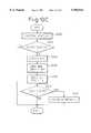
- FIG. 1is a block diagram of a plasma display according to an embodiment of the present invention.
- FIG. 2Ais a waveform diagram showing high-brightness drive waveforms
- FIG. 2Bis a waveform diagram showing low-brightness drive waveforms.
- FIG. 3is a diagram showing an example of operations of a BC signal generating unit according to a first embodiment of the present invention
- FIG. 4is a circuit diagram showing a concrete constitution of the brightness-adjusting unit 11 of FIG. 1.
- FIG. 5is a flow chart showing an operation of the one-chip microcomputer 40 of FIG. 4.
- FIG. 6is a circuit diagram of a brightness-adjusting unit according to a second embodiment of the present invention.
- FIGS. 7A to 7Dare flow charts showing an operation of the one-chip microcomputer 40 of FIG. 6;
- FIG. 8is a block diagram of a display apparatus 200 according to a third embodiment of the present invention.
- FIG. 9is a circuit diagram showing a detailed construction of the MPU 213 in the display apparatus 200 of FIG. 8;
- FIGS. 10A to 10Dare flow charts showing an operation of the control firmware 134 of FIG. 9;
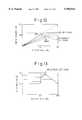
- FIG. 11is a graph explaining an APC control in the third embodiment.
- FIG. 12is a graph showing power consumption versus display rate characteristics of the third embodiment
- FIG. 13is a graph showing brightness value versus display rate characteristics of the third embodiment
- FIG. 14is a diagram showing an example of the operations of the third embodiment.
- FIG. 15is a graph showing power consumption versus display rate characteristics of another embodiment
- FIG. 16is a graph showing brightness value versus display rate characteristics of the embodiment.
- FIG. 17is a block diagram explaining an alternative embodiment, adaptable to each of the foregoing embodiments, providing compensation for brightness deterioration by increasing the APC set point in accordance with measured operating time of a display panel.
- the following description of the inventiondeals with a plasma display device of the two-electrode type using an X-electrode and a Y-electrode. It should, however, be noted that the present invention is in no way limited to such a two-electrode type plasma display device only but can also be adapted to a three-electrode type plasma display device employing an address electrode in addition to the X-electrode and Y-electrode.
- the results the same as those of the two-electrode type plasma display devicecan be obtained by using an X-driver unit, a Y-driver unit and an address driver unit instead of an X-driver unit and a Y-driver unit used in the two-electrode type plasma display device that is described below.
- FIG. 1is a block diagram illustrating a fundamental constitution of a plasma display 10 according to a first embodiment of the present invention.
- the plasma display 10 shown in FIG. 1includes a plasma display panel (PDP) unit 8 having display cells arranged on an X-Y orthogonal matrix, an X-driver unit 6 for selectively driving display cells of a single scanning line according to data to be displayed, a Y-driver unit 7 for selecting the single scanning lines in individual succession for the plural scanning line of the display, a plasma display controller unit 5 for controlling the X- and Y-drivers 6 and 7, and a brightness adjusting unit 11 which is connected to the plasma display controller unit 5 and generates control signals that selectively change the waveform of signals applied to X-driver unit 6 and Y-driver unit 7, between the high-brightness drive waveform and the low-brightness drive waveform, based upon a brightness set value.
- PDPplasma display panel
- the brightness adjusting unit 11includes a variable resistor 1 for manually setting the brightness set value, a BC pulse generator 2 for generating BC pulses whose duration is proportional to the brightness set value, a rising edge detector 22 for detecting rising edges of the BC pulses, a counter 21 for counting H sync from the rising edge of the BC pulses to the trailing edge of the BC pulses and for outputting a count value DA, a counter 23 for counting H sync from the rising edge of the BC pulses and for outputting a count value DB, a BC signal generating unit 20 for generating a stable BC signal, based on count values DA and DB of the counters 21 and 23, and a read only memory 25 for outputting the control signals to be fed to the PDP controller 5, based on the BC signal from the BC signal generating unit 20.
- the BC signal generating unit 20includes, as shown in FIG. 1, input units 12 for inputting data DA and DB from the counters 21 and 23, a storage unit (“RAM") 13 for storing DA as data RD, and an operation unit 30.
- the operation unit 30includes a difference operation unit 14 which reads RD, comprising brightness data DA of one period before (i.e., the next preceding period) and that is stored in the storage unit 13 and which calculates a difference between DA of a current period and RD, a comparator unit 15 for comparing the difference output of unit 14 with a predetermined reference value, and a judging unit 16 which judges whether the variable resistor 1 is operated or not, i.e., whether the set value of the variable resistor 1 is changed or not in response to the output from said comparator unit 15.
- the judging unit 16has a function for judging whether the absolute value of the difference is smaller than, or larger than, the predetermined reference value which, though there is no particular limitation, can be set to be 2. That is, when the absolute value of the difference is not larger than the reference value, it is so judged that the difference is within a range of error and that the variable resistor 1 is not operated. In such a state, therefore, the data RD stored in the storage unit 13 is not updated.
- the storage unit 13is implemented by, for example, RAM and the like.
- the variable resistor 1When the absolute value of the difference is equal to, or larger than, the reference value, it is judged that the variable resistor 1 is operated. In such a state, therefore, the data RD stored in the storage unit 13 is updated using DA.
- the BC signalis input to the most significant bit of an address input of the read only memory 25, and a count value of an address clock (not shown) is input to the other bits of the address input.
- the read only memory 25outputs the control signals by outputting data addressed by the address input.
- the read only memory 25outputs control signals that cause the X-driver 6 and Y-driver 7 to output drive pulses as shown in FIG. 2A.
- the read only memory 25outputs control signals that cause the X-driver 6 and Y-driver 7 to output drive pulses as shown in FIG. 2B.
- X m , X m+1 . . .represents output waveforms of X-driver 6 and Y n , Y n+1 . . . represents output waveforms of Y-driver 7.
- erase pulses 102 following the write pulses 100and data selection pulses 104 for selectively cancelling the erase pulses 102 according to data to be displayed equally appear in FIGS. 2A and 2B, but sustain pulses 106 alternately appear on X-side and Y-side in FIG. 2A, but appear on X-side only in FIG. 2B.
- the sustain pulses alternately applied between X-side and Y-sidecause sustain discharges, but the sustain pulses applied on X-side only cannot cause the sustain discharges.
- FIG. 3shows an example of operations of the BC signal generating unit 20.
- the data DAslightly fluctuates from time t 0 to time t 20 and from time t 24 to time t 28 , but since the difference between DA and RD is less than 2, it is decided that the variable resistor 1 is not operated, and the data RD is hence fixed to 01 or 1A.
- the data DAsuddenly varies from time t 21 to time t 23 , it is decided that the variable resistor 1 is operated, and the data RD is hence changed according to the data DA.
- FIG. 4is a circuit diagram illustrating a concrete constitution of the brightness-adjusting unit 11 of FIG. 1.
- the brightness control (BC) pulse generator 2 connected to the variable resistor 1is implemented by a well-known one-shot multivibrator circuit 2a.
- the rising edge detector 22is implemented by a flip-flop 22a and a NAND circuit 22b.
- the counter 21is implemented by widely known counter IC's 21a and 21b which are connected in series
- the counter 23is implemented by widely known counter IC's 23a and 23b which are connected in series.
- the rising edge of the BC pulseis detected by the NAND circuit 22b, and a clear signal (CLR) is formed for the counters 21 and 23.
- CLRclear signal
- the BC signal generating unit 20 and the read only memory 25 of FIG. 1are implemented by a one-chip microcomputer 40 that contains a central processing unit (CPU), a random access memory (RAM), a read only memory (ROM) and an input/output port.
- a central processing unitCPU
- RAMrandom access memory
- ROMread only memory
- FIG. 5is a flow chart showing an operation of the one-chip microcomputer 40.
- initializationis executed at step 1000.
- operationis executed to read the data DA from the first counter 21.
- the procedurethen proceeds to step 1004 where a difference is found from the stored data RD which is the brightness data of one period before (i.e., the period preceding the current period) as stored in the built-in RAM and where it is judged whether the absolute value of the difference is larger than or equal to a predetermined reference value, e.g., 2 or not.
- a predetermined reference valuee.g. 2 or not.
- the procedureproceeds to step 1006 where the data RD is updated by being replaced by the data DA that is newly input and the procedure proceeds to step 1008.
- the procedurebypasses the step 1006, and the procedure proceeds to step 1008.
- step 1008the counter output value DB of the second counter 23 is read out, and the procedure proceeds to step 1010 where the counter output value DB is compared with the data RD. If the value DB is greater than or equal to the data RD, low-brightness control signals stored in the built-in ROM are read out in step 1012, and if the value DB is less than the data RD, high-brightness control signals stored in the built-in ROM are read out in step 1014. The read-out control signals are output in step 1016, and the procedure returns to step 1002.
- FIG. 6is a circuit diagram illustrating a concrete constitution of a brightness-adjusting unit wherein the APC is introduced according to second embodiment of the present invention.
- a current detecting unit 60is provided for detecting a current Is flowing through a high voltage power source for the PDP.
- the detected current Isis used as an indication of the electric power consumption.
- the current detecting unit 60includes a current mirror circuit 70 for detecting Is as a voltage value, and an integration amplifier 71 that is made up of two inverse amplifiers 72 and 73 connected in series to average the current detected by the current mirror circuit 70 and to match the voltage with an analog input voltage range of a microcomputer 40 that controls the brightness.
- variable resistor 1is directly connected to an analog input port (DBV) of the microcomputer 40.
- DBVanalog input port
- a counter 66 which is connected to the microcomputer 40is constituted in nearly the same manner as the counter 23 shown in FIG. 4 i.e., is constituted by the known counter IC's 66a and 66b connected in series, and its output is fed to the input port (DC) of the microcomputer 40.
- step 1100initialization is executed in step 1100 and then the procedure proceeds to a step 1102 where an APC routine is called.
- step 1205an analog signal that is output from the current-detecting unit 60 and that is input through an analog input port is subjected to an A/D conversion through an analog/digital convertor, to obtain a value DAD.
- the value DADis compared with a predetermined reference value RD1 that has been determined for a current flowing into the display panel.
- RD1a predetermined reference value that has been determined for a current flowing into the display panel.
- step 1206When DAD ⁇ RD1 at the step 1206, i.e., when the value DAD of the detected current is smaller than the reference value RD1, the procedure proceeds to step 1208 where the calculation is carried out to step up the APC output BA by 1, i.e., BA+1.
- step 1206When DAD>RD1 at the step 1206, i.e., when the value DAD of the detected current is larger than the reference value RD1, the procedure proceeds to step 1210 where the calculation is carried out to step down the APC output BA by 1, i.e., BA-1.
- BAexceeds 255 in the above routine, BA is set to 255.
- step 1104a BC routine shown in FIG. 7C is called.
- an analog signal that is output from the variable resistor 1 and that is input through an analog input portis converted into a digital value by using a built-in analog/digital converter, to obtain a value DBV at step 1300.
- step 1302to find a ratio of the APC output BA obtained in the APC routine to BA Max , i.e., to find BA/255 and, then, to effect the correction operation where the value DBV is multiplied by the ratio, i.e., BA/255, and to find the data BB.
- step 1304the data BB of one period before is read out as data RD2. Then, a difference is found between the currently obtained data BB and the data RD2 to judge whether the absolute value of the difference is smaller than, or larger than, a predetermined reference value, e.g., K.
- a predetermined reference valuee.g., K.
- the programproceeds to a step 1306 where the data RD2 is updated by being replaced by the data BB.
- step 1106a CA routine shown in FIG. 7D is called.
- the counted value DC of the signal H sync counted by the counter 66is input to the input port of the microcomputer 40.
- the counted value DCis read out at step 1400.
- the procedureproceeds to a step 1402 where the data RD2 is compared with the value DC.
- the data RD2is greater than the value DC, i.e., when RD2>DC
- the procedureproceeds to step 1402 where the brightness control signal assumes the values "1".
- the procedureproceeds to step 1404 where the brightness control signal assumes the value "0".
- the procedurereturns back to the initial flow chart and at step 1108, access is made to the ROM depending upon the value of the brightness control signal output from the CA routine.
- the ROMoutputs a predetermined display control signal pattern that is stored depending upon the address, and the display drive waveform having high-brightness waveform and low-brightness waveform at a ratio determined by the brightness control signal is fed to the plasma display controller unit 5.
- FIG. 8shows a construction of a display apparatus according to third embodiment of the present invention.
- the display apparatus 200includes a current detection unit 201; a variable resistor 203 for external brightness adjustment; an MPU 213 connected to outputs of the current detection unit 201 and the variable resistor 203; an interface controller 211 connected to signal lines of pixel data DATA-R, DATA-G and DATA-B, a vertical synchronizing signal V sync ,a horizontal synchronizing signal H sync , and a clock signal DCLK; a data controller 212 connected to an output of the interface controller 211; a driver controller 214 connected to outputs of the interface controller 211 and the MPU 213; a Y-driver 215 connected to an output of the driver controller 214 and connected to a Y pulser 216 for driving Y electrodes of a display panel 210; a X pulser 218 connected to the output of the driver controller 214, for driving X electrodes of the display panel 210; and address drivers 217 and 2
- the display apparatus in the present inventionis suitable as a display unit including a device that has a memory function and that is used as a screen of high-brightness, large surface and multiple color display.
- the display apparatusmay be one that needs power consumption control according to the display rate because of large power consumption in a large-sized and high definition display.
- FIG. 9shows detailed construction of the current detection unit 201 and the MPU 213.
- the same reference numerals as used in FIG. 8are used for constituents which are the same as those in FIG. 8.
- the current detection unit 201includes a current mirror circuit 202 for detecting a current Is as a voltage signal, and an integration circuit 204 for averaging the voltage signal Is.
- the MPU 213includes an A/D converter 131 having at least three analog input ports ANO, AN1 and AN2, an arithmetic unit 132, an input/output port 133 and a control firmware 134.
- An output of the variable resistor 203 that outputs a brightness set value BRTis connected to the port AN1.
- the current detection unit 201outputs a power consumption value Is which is connected to the port AN2.
- a variable resistor 205 for adjusting a set point AAP of the power consumption value Isis connected to the port ANO.
- the MPU 213outputs through the input/output port 133 a brightness value MCB consisting of six bit signals MCBC 0-5 to the driver controller 214.
- the driver controller 214outputs drive waveforms that include effective sustain pulses, the number of which within a V sync period is proportional to the brightness value MCB.
- the MPU 213can input, through the input/output port 133, an APC interval (CAP) consisting of two bit signals.
- CAPAPC interval
- CBRBC interval
- FIGS. 10A to 10Dare flow charts showing operations of the control firmware 134 of the MPU 213.
- FIG. 10Ais a main flow chart.
- step 2000initialization of every port of the MPU 213, setting of interruption mode and interruption vectors, and setting of a stack pointer are performed.
- step 2002initial setting, i.e., initial setting of values for every port and register is performed.
- step 2004, an analog value input through the port AN1is A/D-converted in the A/D converter 131 to obtain the brightness set value BRT, which is stored in a register (MCB) in step 2006, and which is output as the brightness value MCB in step 2008.
- step 2010, the MPU 213is enabled for interruptions and, in step 2012, waits for interruptions.
- FIG. 10Bshows an interruption routine which is executed when an interruption occurs.
- an analog value output from the variable resistor 205is A/D-converted in the A/D converter 131 to obtain the set point AAP, which is stored in a register (AAP) in step 2102.
- AAPregister
- AAP-Bis calculated and stored in a register (AAPB).
- the value Bis a predetermined constant value which can be set to be 6, for example.
- an APC routineis called, and in step 2108, a BC routine is called.
- FIG. 10Cshows the APC routine.
- an APC interval counter(CAPU) is incremented by 1 and, in step 2202, the content of (CAPU) is compared with the content of a register (CAP) which stores the APC interval CAP. If the value stored in (CAPU) reaches the value stored in (CAP), then (CAPU) is cleared in step 2204, and an APC processing is executed.
- the brightness set value BRTis input through the port AN1 and the A/D converter 131, and the value BRT is stored in a register (BRT).
- the power consumption value Isis input through the port AN2 and the A/D converter 131, and the value Is is stored in a register (IS).
- the value Is stored in (IS)is compared with the set point AAP stored in (AAP). If (IS) is larger than (AAP), the value stored in (MCB) is decremented by 1 in step 2212.
- FIG. 10Dshows the BC routine.
- a BC interval counterCBRU
- CBRBC interval counter
- the content of (CBRU)is compared with the content of a register (CBR) which stores the BC interval CBR. If the value stored in (CBRU) reaches the value stored in (CBR), the procedure is advance to step 2304, where (CBRU) is cleared.
- the content of (IS)is compared with the content of (AAPB). If the value Is is larger than AAP-B, the procedure is advanced to step 2308 where the brightness set value BRT is compared with the brightness value MCB. If the MCB is larger than BRT, MCB is decremented by 1 in step 2310.
- step 2306BRT is compared with MCB in step 2312. If BRT is larger than MCB, MCB is incremented by 1 in step 2314. If BRT is smaller than MCB, MCB is decremented by 1 in step 2316. In all of the above cases, the procedure is advanced to step 2318 where the MCB thus determined is output to the driver controller 214.
- FIGS. 10A to 10Dshow power consumption versus display rate characteristics and brightness value versus display rate characteristics, respectively, for various different brightness set values, which are obtained in the embodiment explained with reference to FIGS. 10A to 10D.
- the power consumptionis proportionally increased as the display rate is increased, and its gradient is determined by the brightness set value. Nevertheless, the power consumption does not exceed the APC set point, since the brightness value MCB is suppressed as shown in FIG. 13.
- the processing period of the APC routine of FIG. 10Cis determined by the APC interval CAP, and the processing period of the BC routine of FIG. 10D is determined by the BC interval CBR.
- CAP and CBRmay be given as constants in advance.
- CAP and CBRcan be externally set by the switch 206 of FIG. 9.
- Is becomes larger than AAPbecause of a sudden increase in the display rate
- MCBis gradually decreased at a speed determined by CAP.
- MCBis gradually increased at a speed determined by CBR.
- the APC interval CAPis greater than the BC interval CBR.
- FIG. 14shows an example of operations of the third embodiment.
- the APC set pointis set at 0.6 of the maximum power consumption.
- the display rateis 100% and the brightness set value is a maximum at time t 0 .
- the power consumptionrises up to its maximum since the brightness value is set at its maximum by steps 2006 and 2008 of FIG. 10A.
- the power consumptionis gradually decreased by gradually decreasing the brightness value in step 2212 of FIG. 10C and is settled at the APC set point 0.6 from t 1 to t 2 .
- the display ratedecreases to 50% at t 2
- the power consumptiondecreases and therefore the brightness value is gradually increased up to its maximum level by step 2314 of FIG. 10D.
- the brightness set valueis changed to its minimum level. Then, the brightness value is gradually decreased until the brightness value becomes equal to the brightness set value by step 2316 of FIG. 10D.
- the display rateincreases to 100%, but since the power consumption does not exceed the APC set point, the brightness value is not changed.
- the brightness valueis gradually increased until the power consumption reaches the APC set point at time t 7 .
- the display ratedecreases to 50% at time t 8 , the brightness value is changed to its maximum level since the power consumption decreases below the APC set point and the brightness set value is at the maximum level. After that, when the display rate changes to 100%, the brightness value is gradually decreased to decrease the power consumption to the set point.
- the APC set pointis fixed to the set value of the variable register 205. Therefore, the brightness of the PDP cannot be manually changed while the brightness value is suppressed by the APC routine (APC-first mode).
- APC-first modethe brightness of the PDP cannot be manually changed while the brightness value is suppressed by the APC routine
- the brightnessis always manually adjustable, this is realized by varying the APC set point by multiplying it by the brightness set value (BC-first mode). It is preferable that an operation mode is externally selectable between the above two operation modes according to the use of the display device.
- the consumed poweris detected by detecting the current assuming that power voltages are equal with regard to individual PDPs, in the above embodiment.
- the consumed power or the APC set pointcan be corrected by detecting the power voltage VS using a suitable voltage divider 205 and the A/D converter 131.
- the power consumptionthat is to say, the brightness of the whole PDP display
- the power consumptionis linearly decreased as the display rate decreases, as shown in FIG. 12.
- Brightness of the whole PDPcan be maintained to a certain extent, as shown in FIG. 15, by controlling the brightness value as a function of the display rate, and which can be estimated from the brightness value and the power consumption, as shown in FIG. 16.
- a PDPeffectively comprises discharge tubes (i.e., an array of gaseous discharge cells)
- the brightness of the PDPdeteriorates after it is used for a long time.
- the brightness deteriorationcan be compensated by counting operating time in a counter 92 of FIG. 17, and by increasing the APC set point according to the operating time.
Landscapes
- Engineering & Computer Science (AREA)
- Physics & Mathematics (AREA)
- Power Engineering (AREA)
- Plasma & Fusion (AREA)
- Computer Hardware Design (AREA)
- General Physics & Mathematics (AREA)
- Theoretical Computer Science (AREA)
- Control Of Indicators Other Than Cathode Ray Tubes (AREA)
- Control Of Gas Discharge Display Tubes (AREA)
Abstract
Description
Claims (51)
Applications Claiming Priority (4)
| Application Number | Priority Date | Filing Date | Title |
|---|---|---|---|
| JP6-253618 | 1994-10-19 | ||
| JP25361894AJP3489882B2 (en) | 1994-10-19 | 1994-10-19 | Plasma display, drive control device thereof, and drive method thereof |
| JP7-109703 | 1995-05-08 | ||
| JP07109703AJP3142458B2 (en) | 1995-05-08 | 1995-05-08 | Display device control method and display device |
Publications (1)
| Publication Number | Publication Date |
|---|---|
| US5956014Atrue US5956014A (en) | 1999-09-21 |
Family
ID=26449436
Family Applications (1)
| Application Number | Title | Priority Date | Filing Date |
|---|---|---|---|
| US08/544,590Expired - LifetimeUS5956014A (en) | 1994-10-19 | 1995-10-18 | Brightness control and power control of display device |
Country Status (2)
| Country | Link |
|---|---|
| US (1) | US5956014A (en) |
| KR (3) | KR100251624B1 (en) |
Cited By (79)
| Publication number | Priority date | Publication date | Assignee | Title |
|---|---|---|---|---|
| US6278421B1 (en)* | 1996-11-06 | 2001-08-21 | Fujitsu Limited | Method and apparatus for controlling power consumption of display unit, display system equipped with the same, and storage medium with program stored therein for implementing the same |
| US6288495B1 (en)* | 1999-03-30 | 2001-09-11 | Nec Corporation | Driving apparatus for plasma display panel |
| US6326938B1 (en)* | 1998-03-26 | 2001-12-04 | Fujitsu Limited | Power consumption control in display unit |
| US6351253B2 (en)* | 1997-12-10 | 2002-02-26 | Matsushita Electric Industrial Co., Ltd. | Display apparatus capable of adjusting subfield number according to brightness |
| US6388716B1 (en)* | 1997-12-25 | 2002-05-14 | Kabushiki Kaisha Toshiba | Automatic brightness correction apparatus for image display device |
| US20020118312A1 (en)* | 2001-02-27 | 2002-08-29 | Nec Corporation | Plasma display and driving method of the same |
| EP1089112A3 (en)* | 1999-09-27 | 2002-10-02 | Seiko Epson Corporation | IC-driver circuit for an electro-optical device |
| US20020154073A1 (en)* | 2000-09-25 | 2002-10-24 | Fujitsu Hitachi Plasma Display Limited | Display apparatus |
| US6496165B1 (en)* | 1999-07-01 | 2002-12-17 | Pioneer Corporation | Driving apparatus for driving a plasma display panel based on power consumed during a non-light emitting period of a unit display period |
| US20030001804A1 (en)* | 2001-06-28 | 2003-01-02 | Pioneer Corporation And Shizuoka Pioneer Corporation | Drive method and drive apparatus for a display panel |
| US20030001802A1 (en)* | 2001-06-29 | 2003-01-02 | Pioneer Corporation And Shizuoka Pioneer Corporation | Plasma display panel unit |
| US20030011543A1 (en)* | 2001-07-11 | 2003-01-16 | Pioneer Corporation | Display controller and display apparatus |
| US20030030655A1 (en)* | 2001-08-08 | 2003-02-13 | Fujitsu Hitachi Plasma Display Limited | Display device capable of controlling power consumption without generating degradation in image quality, and method of driving the display device |
| US20030098824A1 (en)* | 2001-11-28 | 2003-05-29 | Lg Electronics Inc. | Setting method for average picture level and method of driving plasma display panel using the same |
| KR20030072798A (en)* | 2002-03-06 | 2003-09-19 | 엘지전자 주식회사 | Apparatus and method of driving plasma display panel |
| US20030193472A1 (en)* | 1999-10-28 | 2003-10-16 | Powell John P. | Display brightness control method and apparatus for conserving battery power |
| US20030218432A1 (en)* | 2002-05-24 | 2003-11-27 | Yoo-Jin Song | Automatic power control (APC) method and device of plasma display panel (PDP) and PDP device having the APC device |
| US20030222841A1 (en)* | 2002-05-30 | 2003-12-04 | Fujitsu Limited | Signal processing unit and liquid crystal display device |
| US20040027322A1 (en)* | 2000-08-01 | 2004-02-12 | Hannstar Display Corp. | Method and apparatus for dynamic gray level switching |
| US6724356B1 (en) | 1999-06-30 | 2004-04-20 | Fujitsu Limited | Plasma display unit |
| US6734840B2 (en)* | 1999-12-14 | 2004-05-11 | Fujitsu Display Technologies Corporation | Liquid crystal display device with judging section |
| US6778160B2 (en)* | 2000-01-17 | 2004-08-17 | International Business Machines Corporation | Liquid-crystal display, liquid-crystal control circuit, flicker inhibition method, and liquid-crystal driving method |
| US20050140587A1 (en)* | 2003-10-21 | 2005-06-30 | Cho Dae S. | Method and apparatus for decreasing an afterimage of a plasma display panel |
| US20050270283A1 (en)* | 2003-07-16 | 2005-12-08 | Plut William J | Methods for spatial-based power savings |
| US20050270265A1 (en)* | 2003-07-16 | 2005-12-08 | Plut William J | LCD plateau power conservation |
| US20060001660A1 (en)* | 2003-07-16 | 2006-01-05 | Plut William J | Color preservation for spatially varying power conservation |
| US20060001659A1 (en)* | 2003-07-16 | 2006-01-05 | Plut William J | Window information preservation for spatially varying power conservation |
| US20060001658A1 (en)* | 2003-07-16 | 2006-01-05 | Plut William J | Edge preservation for spatially varying power conservation |
| US20060010488A1 (en)* | 2004-07-07 | 2006-01-12 | Fujitsu Limited | Server system and server |
| US20060020906A1 (en)* | 2003-07-16 | 2006-01-26 | Plut William J | Graphics preservation for spatially varying display device power conversation |
| US20060050029A1 (en)* | 2004-09-07 | 2006-03-09 | Hitachi Displays, Ltd. | Display device |
| US20060119612A1 (en)* | 2004-12-02 | 2006-06-08 | Kerofsky Louis J | Methods and systems for image-specific tone scale adjustment and light-source control |
| US20060236893A1 (en)* | 2005-04-22 | 2006-10-26 | Xerox Corporation | Photoreceptors |
| US20060250525A1 (en)* | 2005-05-04 | 2006-11-09 | Plut William J | White-based power savings |
| US20060284822A1 (en)* | 2004-12-02 | 2006-12-21 | Sharp Laboratories Of America, Inc. | Methods and systems for enhancing display characteristics |
| US20070002035A1 (en)* | 2003-07-16 | 2007-01-04 | Plut William J | Background plateau manipulation for display device power conservation |
| CN1329879C (en)* | 2004-11-03 | 2007-08-01 | 东南大学 | Drive circuit for plasma display screen |
| US20080024517A1 (en)* | 2006-07-28 | 2008-01-31 | Louis Joseph Kerofsky | Systems and methods for color preservation with image tone scale corrections |
| US20080042600A1 (en)* | 2004-11-29 | 2008-02-21 | Toru Teraoka | Display Apparatus and Method for Driving the Same |
| US20080174773A1 (en)* | 2007-01-18 | 2008-07-24 | Hinds Instruments Inc. | Sample Holder for an Optical Element |
| EP1398757A3 (en)* | 2002-09-13 | 2008-12-17 | Samsung Electronics Co., Ltd. | Image brightness and colour temperature control |
| US20090225006A1 (en)* | 2005-08-04 | 2009-09-10 | Makoto Onozawa | Plasma Display Apparatus |
| US20090231320A1 (en)* | 2005-07-06 | 2009-09-17 | Ken Kumakura | Plasma Display Device |
| US20100026735A1 (en)* | 2005-05-04 | 2010-02-04 | Plut William J | Luminance suppression power conservation |
| US7768496B2 (en) | 2004-12-02 | 2010-08-03 | Sharp Laboratories Of America, Inc. | Methods and systems for image tonescale adjustment to compensate for a reduced source light power level |
| US7782405B2 (en) | 2004-12-02 | 2010-08-24 | Sharp Laboratories Of America, Inc. | Systems and methods for selecting a display source light illumination level |
| US20100214325A1 (en)* | 2007-10-05 | 2010-08-26 | Daisuke Koyama | Image display |
| US7826681B2 (en) | 2007-02-28 | 2010-11-02 | Sharp Laboratories Of America, Inc. | Methods and systems for surround-specific display modeling |
| US7839406B2 (en)* | 2006-03-08 | 2010-11-23 | Sharp Laboratories Of America, Inc. | Methods and systems for enhancing display characteristics with ambient illumination input |
| US20100315572A1 (en)* | 2009-06-15 | 2010-12-16 | Maxim Integrated Products, Inc. | Circuit topology for driving high-voltage led series connected strings |
| US7924261B2 (en) | 2004-12-02 | 2011-04-12 | Sharp Laboratories Of America, Inc. | Methods and systems for determining a display light source adjustment |
| EP2093747A4 (en)* | 2006-11-27 | 2011-04-13 | Panasonic Corp | LUMINANCE RATE CONTROLLER |
| US7982707B2 (en) | 2004-12-02 | 2011-07-19 | Sharp Laboratories Of America, Inc. | Methods and systems for generating and applying image tone scale adjustments |
| US8004511B2 (en) | 2004-12-02 | 2011-08-23 | Sharp Laboratories Of America, Inc. | Systems and methods for distortion-related source light management |
| US8111265B2 (en) | 2004-12-02 | 2012-02-07 | Sharp Laboratories Of America, Inc. | Systems and methods for brightness preservation using a smoothed gain image |
| US20120041641A1 (en)* | 2010-08-10 | 2012-02-16 | Nissan Motor Co., Ltd. | Stability display apparatus |
| US8120570B2 (en) | 2004-12-02 | 2012-02-21 | Sharp Laboratories Of America, Inc. | Systems and methods for tone curve generation, selection and application |
| US8155434B2 (en) | 2007-10-30 | 2012-04-10 | Sharp Laboratories Of America, Inc. | Methods and systems for image enhancement |
| US8165724B2 (en) | 2009-06-17 | 2012-04-24 | Sharp Laboratories Of America, Inc. | Methods and systems for power-controlling display devices |
| US8169431B2 (en) | 2007-12-26 | 2012-05-01 | Sharp Laboratories Of America, Inc. | Methods and systems for image tonescale design |
| US8179363B2 (en) | 2007-12-26 | 2012-05-15 | Sharp Laboratories Of America, Inc. | Methods and systems for display source light management with histogram manipulation |
| US8203579B2 (en) | 2007-12-26 | 2012-06-19 | Sharp Laboratories Of America, Inc. | Methods and systems for backlight modulation with image characteristic mapping |
| US8207932B2 (en) | 2007-12-26 | 2012-06-26 | Sharp Laboratories Of America, Inc. | Methods and systems for display source light illumination level selection |
| US8223113B2 (en) | 2007-12-26 | 2012-07-17 | Sharp Laboratories Of America, Inc. | Methods and systems for display source light management with variable delay |
| US8305401B1 (en)* | 2009-04-27 | 2012-11-06 | Maxim Integrated, Inc. | Digital light management controller |
| US8345038B2 (en) | 2007-10-30 | 2013-01-01 | Sharp Laboratories Of America, Inc. | Methods and systems for backlight modulation and brightness preservation |
| US8378956B2 (en) | 2007-11-30 | 2013-02-19 | Sharp Laboratories Of America, Inc. | Methods and systems for weighted-error-vector-based source light selection |
| US8416179B2 (en) | 2008-07-10 | 2013-04-09 | Sharp Laboratories Of America, Inc. | Methods and systems for color preservation with a color-modulated backlight |
| US8522059B2 (en) | 2009-11-24 | 2013-08-27 | Hewlett-Packard Development Company, L.P. | Display panel power prediction |
| US8531379B2 (en) | 2008-04-28 | 2013-09-10 | Sharp Laboratories Of America, Inc. | Methods and systems for image compensation for ambient conditions |
| US8742685B1 (en) | 2010-04-05 | 2014-06-03 | Maxim Integrated Products, Inc. | Magnetic amplifier assisted LED constant current sink overhead voltage regulation |
| US8913089B2 (en) | 2005-06-15 | 2014-12-16 | Sharp Laboratories Of America, Inc. | Methods and systems for enhancing display characteristics with frequency-specific gain |
| US8922594B2 (en) | 2005-06-15 | 2014-12-30 | Sharp Laboratories Of America, Inc. | Methods and systems for enhancing display characteristics with high frequency contrast enhancement |
| US8947465B2 (en) | 2004-12-02 | 2015-02-03 | Sharp Laboratories Of America, Inc. | Methods and systems for display-mode-dependent brightness preservation |
| US9083969B2 (en) | 2005-08-12 | 2015-07-14 | Sharp Laboratories Of America, Inc. | Methods and systems for independent view adjustment in multiple-view displays |
| US9177509B2 (en) | 2007-11-30 | 2015-11-03 | Sharp Laboratories Of America, Inc. | Methods and systems for backlight modulation with scene-cut detection |
| US9330630B2 (en) | 2008-08-30 | 2016-05-03 | Sharp Laboratories Of America, Inc. | Methods and systems for display source light management with rate change control |
| WO2021060808A1 (en)* | 2019-09-24 | 2021-04-01 | Lg Electronics Inc. | Signal processing device and image display apparatus including same |
| US12217677B2 (en) | 2022-10-25 | 2025-02-04 | Samsung Display Co., Ltd. | Display device, method of driving display device, and electronic apparatus including display device |
Families Citing this family (4)
| Publication number | Priority date | Publication date | Assignee | Title |
|---|---|---|---|---|
| DE60125637T2 (en)* | 2000-05-17 | 2007-10-04 | International Business Machines Corp. | System and method to detect the residence or availability of a telephone user and to publish the telephone number on the Internet |
| KR20040038303A (en)* | 2002-10-31 | 2004-05-08 | 삼성전자주식회사 | Low power consumption PDP with high speed response |
| JP2005099713A (en) | 2003-08-25 | 2005-04-14 | Seiko Epson Corp | Electro-optical device, driving method of electro-optical device, and electronic apparatus |
| KR101058155B1 (en) | 2010-09-13 | 2011-08-24 | 양순옥 | Method and device for saving measured value of sensor that store only deviation of measured value in sensor network in separate storage area of memory |
Citations (10)
| Publication number | Priority date | Publication date | Assignee | Title |
|---|---|---|---|---|
| US4044375A (en)* | 1976-08-19 | 1977-08-23 | Rca Corporation | Brightness control apparatus |
| US4394689A (en)* | 1981-07-13 | 1983-07-19 | The United States Of America As Represented By The Secretary Of The Navy | Programmable CRT brightness control |
| US4547797A (en)* | 1982-10-12 | 1985-10-15 | Sperry Corporation | Apparatus for color tracking and brightness correction for multi-gun color cathode ray tube display |
| JPH02187788A (en)* | 1989-01-13 | 1990-07-23 | Matsushita Electric Ind Co Ltd | Active matrix liquid crystal display device |
| JPH03282582A (en)* | 1990-03-30 | 1991-12-12 | Fujitsu Ltd | plasma display device |
| JPH0411281A (en)* | 1990-04-28 | 1992-01-16 | Sharp Corp | Simple matrix type liquid crystal display device |
| JPH0451285A (en)* | 1990-06-19 | 1992-02-19 | Oki Electric Ind Co Ltd | Color plasma display |
| JPH06202580A (en)* | 1993-01-07 | 1994-07-22 | Fujitsu Ltd | Plasma display device |
| US5347294A (en)* | 1991-04-17 | 1994-09-13 | Casio Computer Co., Ltd. | Image display apparatus |
| US5583527A (en)* | 1993-11-26 | 1996-12-10 | Fujitsu Limited | Flat display |
- 1995
- 1995-10-18USUS08/544,590patent/US5956014A/ennot_activeExpired - Lifetime
- 1995-10-19KRKR1019950036155Apatent/KR100251624B1/ennot_activeExpired - Fee Related
- 1999
- 1999-09-21KRKR1019990040643Apatent/KR100330736B1/ennot_activeExpired - Fee Related
- 1999-09-21KRKR1019990040642Apatent/KR100389643B1/ennot_activeExpired - Fee Related
Patent Citations (10)
| Publication number | Priority date | Publication date | Assignee | Title |
|---|---|---|---|---|
| US4044375A (en)* | 1976-08-19 | 1977-08-23 | Rca Corporation | Brightness control apparatus |
| US4394689A (en)* | 1981-07-13 | 1983-07-19 | The United States Of America As Represented By The Secretary Of The Navy | Programmable CRT brightness control |
| US4547797A (en)* | 1982-10-12 | 1985-10-15 | Sperry Corporation | Apparatus for color tracking and brightness correction for multi-gun color cathode ray tube display |
| JPH02187788A (en)* | 1989-01-13 | 1990-07-23 | Matsushita Electric Ind Co Ltd | Active matrix liquid crystal display device |
| JPH03282582A (en)* | 1990-03-30 | 1991-12-12 | Fujitsu Ltd | plasma display device |
| JPH0411281A (en)* | 1990-04-28 | 1992-01-16 | Sharp Corp | Simple matrix type liquid crystal display device |
| JPH0451285A (en)* | 1990-06-19 | 1992-02-19 | Oki Electric Ind Co Ltd | Color plasma display |
| US5347294A (en)* | 1991-04-17 | 1994-09-13 | Casio Computer Co., Ltd. | Image display apparatus |
| JPH06202580A (en)* | 1993-01-07 | 1994-07-22 | Fujitsu Ltd | Plasma display device |
| US5583527A (en)* | 1993-11-26 | 1996-12-10 | Fujitsu Limited | Flat display |
Non-Patent Citations (2)
| Title |
|---|
| Kawada et al., Plasma Display Device, Patent Abstracts of Japan (Fujitsu Ltd) & JP 03282582 A, Dec. 12, 1991.* |
| Toyama et al., Color Plasma Display, Patent Abstracts of Japan (Oki Electric Ind Co Ltd) & JP 04051285 A, Feb. 19, 1992.* |
Cited By (135)
| Publication number | Priority date | Publication date | Assignee | Title |
|---|---|---|---|---|
| US6278421B1 (en)* | 1996-11-06 | 2001-08-21 | Fujitsu Limited | Method and apparatus for controlling power consumption of display unit, display system equipped with the same, and storage medium with program stored therein for implementing the same |
| US6351253B2 (en)* | 1997-12-10 | 2002-02-26 | Matsushita Electric Industrial Co., Ltd. | Display apparatus capable of adjusting subfield number according to brightness |
| US6388716B1 (en)* | 1997-12-25 | 2002-05-14 | Kabushiki Kaisha Toshiba | Automatic brightness correction apparatus for image display device |
| US6326938B1 (en)* | 1998-03-26 | 2001-12-04 | Fujitsu Limited | Power consumption control in display unit |
| US6288495B1 (en)* | 1999-03-30 | 2001-09-11 | Nec Corporation | Driving apparatus for plasma display panel |
| US6724356B1 (en) | 1999-06-30 | 2004-04-20 | Fujitsu Limited | Plasma display unit |
| US6496165B1 (en)* | 1999-07-01 | 2002-12-17 | Pioneer Corporation | Driving apparatus for driving a plasma display panel based on power consumed during a non-light emitting period of a unit display period |
| US20080094328A1 (en)* | 1999-09-27 | 2008-04-24 | Seiko Epson Corporation | Electro-Optical Device, and Electronic Apparatus and Display Driver IC Using the Same |
| US20050024308A1 (en)* | 1999-09-27 | 2005-02-03 | Seiko Epson Corporation | Electro-optical device, and electronic apparatus and display driver IC using the same |
| EP1089112A3 (en)* | 1999-09-27 | 2002-10-02 | Seiko Epson Corporation | IC-driver circuit for an electro-optical device |
| US6937216B1 (en) | 1999-09-27 | 2005-08-30 | Seiko Epson Corporation | Electro-optical device, and electronic apparatus and display driver IC using the same |
| US7312775B2 (en) | 1999-09-27 | 2007-12-25 | Seiko Epson Corporation | Electro-optical device, and electronic apparatus and display driver IC using the same |
| US6731274B2 (en)* | 1999-10-28 | 2004-05-04 | Gateway, Inc. | Display brightness control method and apparatus for conserving battery power |
| US20030193472A1 (en)* | 1999-10-28 | 2003-10-16 | Powell John P. | Display brightness control method and apparatus for conserving battery power |
| US6734840B2 (en)* | 1999-12-14 | 2004-05-11 | Fujitsu Display Technologies Corporation | Liquid crystal display device with judging section |
| US6778160B2 (en)* | 2000-01-17 | 2004-08-17 | International Business Machines Corporation | Liquid-crystal display, liquid-crystal control circuit, flicker inhibition method, and liquid-crystal driving method |
| US20040027322A1 (en)* | 2000-08-01 | 2004-02-12 | Hannstar Display Corp. | Method and apparatus for dynamic gray level switching |
| US7248241B2 (en)* | 2000-08-01 | 2007-07-24 | Hannstar Display Corp. | Method and apparatus for dynamic gray level switching |
| US7944407B2 (en) | 2000-09-25 | 2011-05-17 | Fujitsu Hitachi Plasma Display Limited | Display apparatus |
| US8947324B2 (en)* | 2000-09-25 | 2015-02-03 | Hitachi Maxell, Ltd. | Display apparatus |
| US20080284687A1 (en)* | 2000-09-25 | 2008-11-20 | Fujitsu Hitachi Plasma Display | Display apparatus |
| US20100141691A1 (en)* | 2000-09-25 | 2010-06-10 | Fujitsu Hitachi Plasma Display | Display apparatus |
| US20020154073A1 (en)* | 2000-09-25 | 2002-10-24 | Fujitsu Hitachi Plasma Display Limited | Display apparatus |
| US7088312B2 (en)* | 2001-02-27 | 2006-08-08 | Pioneer Corporation | Plasma display and driving method of the same |
| US20020118312A1 (en)* | 2001-02-27 | 2002-08-29 | Nec Corporation | Plasma display and driving method of the same |
| US7133008B2 (en) | 2001-06-28 | 2006-11-07 | Pioneer Corporation | Drive method and drive apparatus for a display panel |
| EP1274064A3 (en)* | 2001-06-28 | 2004-07-28 | Pioneer Corporation | Drive method and drive apparatus for a display panel |
| US20030001804A1 (en)* | 2001-06-28 | 2003-01-02 | Pioneer Corporation And Shizuoka Pioneer Corporation | Drive method and drive apparatus for a display panel |
| US20030001802A1 (en)* | 2001-06-29 | 2003-01-02 | Pioneer Corporation And Shizuoka Pioneer Corporation | Plasma display panel unit |
| US6954186B2 (en)* | 2001-06-29 | 2005-10-11 | Pioneer Corporation | Plasma display panel unit |
| EP1271464A3 (en)* | 2001-06-29 | 2004-10-20 | Pioneer Corporation | Plasma display panel unit |
| EP1276097A3 (en)* | 2001-07-11 | 2004-11-24 | Pioneer Corporation | Display controller and display apparatus |
| US6967646B2 (en) | 2001-07-11 | 2005-11-22 | Pioneer Corporation | Display controller and display apparatus |
| US20030011543A1 (en)* | 2001-07-11 | 2003-01-16 | Pioneer Corporation | Display controller and display apparatus |
| US7423611B2 (en) | 2001-08-08 | 2008-09-09 | Fujitsu Hitachi Plasma Display Limited | Display device capable of controlling power consumption without generating degradation in image quality, and method of driving the display device |
| US20030030655A1 (en)* | 2001-08-08 | 2003-02-13 | Fujitsu Hitachi Plasma Display Limited | Display device capable of controlling power consumption without generating degradation in image quality, and method of driving the display device |
| US20030098824A1 (en)* | 2001-11-28 | 2003-05-29 | Lg Electronics Inc. | Setting method for average picture level and method of driving plasma display panel using the same |
| US7057585B2 (en)* | 2001-11-28 | 2006-06-06 | Lg Electronics Inc. | Setting method for average picture level and method of driving plasma display panel using the same |
| KR20030072798A (en)* | 2002-03-06 | 2003-09-19 | 엘지전자 주식회사 | Apparatus and method of driving plasma display panel |
| US6794824B2 (en)* | 2002-05-24 | 2004-09-21 | Samsung Sdi Co., Ltd. | Automatic power control (APC) method and device of plasma display panel (PDP) and PDP device having the APC device |
| US20030218432A1 (en)* | 2002-05-24 | 2003-11-27 | Yoo-Jin Song | Automatic power control (APC) method and device of plasma display panel (PDP) and PDP device having the APC device |
| US7167214B2 (en)* | 2002-05-30 | 2007-01-23 | Fujitsu Hitachi Plasma Display Limited | Signal processing unit and liquid crystal display device |
| US20030222841A1 (en)* | 2002-05-30 | 2003-12-04 | Fujitsu Limited | Signal processing unit and liquid crystal display device |
| EP1398757A3 (en)* | 2002-09-13 | 2008-12-17 | Samsung Electronics Co., Ltd. | Image brightness and colour temperature control |
| US20100079595A1 (en)* | 2003-07-16 | 2010-04-01 | Plut William J | Televisions with reduced power consumption |
| US20100220090A1 (en)* | 2003-07-16 | 2010-09-02 | Plut William J | Background plateau manipulation for display device power conservation |
| US8207934B2 (en) | 2003-07-16 | 2012-06-26 | Samsung Electronics Co., Ltd | Spatial based power savings for LCD televisions |
| US8912999B2 (en) | 2003-07-16 | 2014-12-16 | Samsung Electronics Co., Ltd. | Background plateau manipulation for display device power conservation |
| US20070002035A1 (en)* | 2003-07-16 | 2007-01-04 | Plut William J | Background plateau manipulation for display device power conservation |
| US8203551B2 (en) | 2003-07-16 | 2012-06-19 | Samsung Electronics Co., Ltd | Televisions with reduced power consumption |
| US9135884B2 (en) | 2003-07-16 | 2015-09-15 | Samsung Electronics Co., Ltd. | LCD plateau power conservation |
| US9715846B2 (en) | 2003-07-16 | 2017-07-25 | Samsung Electronics Co., Ltd. | Background plateau manipulation for display device power conservation |
| US7714831B2 (en) | 2003-07-16 | 2010-05-11 | Honeywood Technologies, Llc | Background plateau manipulation for display device power conservation |
| US20060001658A1 (en)* | 2003-07-16 | 2006-01-05 | Plut William J | Edge preservation for spatially varying power conservation |
| US7786988B2 (en) | 2003-07-16 | 2010-08-31 | Honeywood Technologies, Llc | Window information preservation for spatially varying power conservation |
| US20100149197A1 (en)* | 2003-07-16 | 2010-06-17 | Plut William J | Spatial based power savings for lcd televisions |
| US20060001659A1 (en)* | 2003-07-16 | 2006-01-05 | Plut William J | Window information preservation for spatially varying power conservation |
| US20100141635A1 (en)* | 2003-07-16 | 2010-06-10 | Plut William J | Lcd plateau power conservation |
| US20060001660A1 (en)* | 2003-07-16 | 2006-01-05 | Plut William J | Color preservation for spatially varying power conservation |
| US20050275651A1 (en)* | 2003-07-16 | 2005-12-15 | Plut William J | Histogram and spatial-based power savings |
| US20060020906A1 (en)* | 2003-07-16 | 2006-01-26 | Plut William J | Graphics preservation for spatially varying display device power conversation |
| US7663597B2 (en) | 2003-07-16 | 2010-02-16 | Honeywood Technologies, Llc | LCD plateau power conservation |
| US20050270283A1 (en)* | 2003-07-16 | 2005-12-08 | Plut William J | Methods for spatial-based power savings |
| US7580031B2 (en) | 2003-07-16 | 2009-08-25 | Honeywood Technologies, Llc | Histogram and spatial-based power savings |
| US7583260B2 (en) | 2003-07-16 | 2009-09-01 | Honeywood Technologies, Llc | Color preservation for spatially varying power conservation |
| US9953553B2 (en) | 2003-07-16 | 2018-04-24 | Samsung Electronics Co., Ltd. | Background plateau manipulation for display device power conservation |
| US20050270265A1 (en)* | 2003-07-16 | 2005-12-08 | Plut William J | LCD plateau power conservation |
| US7602388B2 (en) | 2003-07-16 | 2009-10-13 | Honeywood Technologies, Llc | Edge preservation for spatially varying power conservation |
| US7629971B2 (en) | 2003-07-16 | 2009-12-08 | Honeywood Technologies, Llc | Methods for spatial-based power savings |
| EP1526500A3 (en)* | 2003-10-21 | 2007-02-28 | Lg Electronics Inc. | Method and apparatus for decreasing an afterimage of a plasma display panel |
| US20050140587A1 (en)* | 2003-10-21 | 2005-06-30 | Cho Dae S. | Method and apparatus for decreasing an afterimage of a plasma display panel |
| US20060010488A1 (en)* | 2004-07-07 | 2006-01-12 | Fujitsu Limited | Server system and server |
| US7479953B2 (en)* | 2004-09-07 | 2009-01-20 | Hitachi Displays, Ltd. | Display device |
| US20060050029A1 (en)* | 2004-09-07 | 2006-03-09 | Hitachi Displays, Ltd. | Display device |
| CN1329879C (en)* | 2004-11-03 | 2007-08-01 | 东南大学 | Drive circuit for plasma display screen |
| US20080042600A1 (en)* | 2004-11-29 | 2008-02-21 | Toru Teraoka | Display Apparatus and Method for Driving the Same |
| US7782405B2 (en) | 2004-12-02 | 2010-08-24 | Sharp Laboratories Of America, Inc. | Systems and methods for selecting a display source light illumination level |
| US7800577B2 (en) | 2004-12-02 | 2010-09-21 | Sharp Laboratories Of America, Inc. | Methods and systems for enhancing display characteristics |
| US8111265B2 (en) | 2004-12-02 | 2012-02-07 | Sharp Laboratories Of America, Inc. | Systems and methods for brightness preservation using a smoothed gain image |
| US8947465B2 (en) | 2004-12-02 | 2015-02-03 | Sharp Laboratories Of America, Inc. | Methods and systems for display-mode-dependent brightness preservation |
| US8004511B2 (en) | 2004-12-02 | 2011-08-23 | Sharp Laboratories Of America, Inc. | Systems and methods for distortion-related source light management |
| US7982707B2 (en) | 2004-12-02 | 2011-07-19 | Sharp Laboratories Of America, Inc. | Methods and systems for generating and applying image tone scale adjustments |
| US20060119612A1 (en)* | 2004-12-02 | 2006-06-08 | Kerofsky Louis J | Methods and systems for image-specific tone scale adjustment and light-source control |
| US8120570B2 (en) | 2004-12-02 | 2012-02-21 | Sharp Laboratories Of America, Inc. | Systems and methods for tone curve generation, selection and application |
| US7961199B2 (en) | 2004-12-02 | 2011-06-14 | Sharp Laboratories Of America, Inc. | Methods and systems for image-specific tone scale adjustment and light-source control |
| US7924261B2 (en) | 2004-12-02 | 2011-04-12 | Sharp Laboratories Of America, Inc. | Methods and systems for determining a display light source adjustment |
| US7768496B2 (en) | 2004-12-02 | 2010-08-03 | Sharp Laboratories Of America, Inc. | Methods and systems for image tonescale adjustment to compensate for a reduced source light power level |
| US20060284822A1 (en)* | 2004-12-02 | 2006-12-21 | Sharp Laboratories Of America, Inc. | Methods and systems for enhancing display characteristics |
| US20110001757A1 (en)* | 2004-12-02 | 2011-01-06 | Sharp Laboratories Of America, Inc. | Method and apparatus for adjusting an image to enhance display characteristics |
| US20060236893A1 (en)* | 2005-04-22 | 2006-10-26 | Xerox Corporation | Photoreceptors |
| US7760210B2 (en) | 2005-05-04 | 2010-07-20 | Honeywood Technologies, Llc | White-based power savings |
| US20100277648A1 (en)* | 2005-05-04 | 2010-11-04 | Plut William J | White-based power savings |
| US20100026735A1 (en)* | 2005-05-04 | 2010-02-04 | Plut William J | Luminance suppression power conservation |
| US11145270B2 (en) | 2005-05-04 | 2021-10-12 | Samsung Electronics Co., Ltd. | Luminance suppression power conservation |
| US9785215B2 (en) | 2005-05-04 | 2017-10-10 | Samsung Electronics Co., Ltd. | White-based power savings |
| US9659544B2 (en) | 2005-05-04 | 2017-05-23 | Samsung Electronics Co., Ltd. | Luminance suppression power conservation |
| US10685620B2 (en) | 2005-05-04 | 2020-06-16 | Samsung Electronics Co., Ltd. | Luminance suppression power conservation |
| US10140945B2 (en) | 2005-05-04 | 2018-11-27 | Samsung Electronics Co., Ltd. | Luminance suppression power conservation |
| US20100026736A1 (en)* | 2005-05-04 | 2010-02-04 | Plut William J | Luminance suppression power conservation |
| US20060250525A1 (en)* | 2005-05-04 | 2006-11-09 | Plut William J | White-based power savings |
| US8922594B2 (en) | 2005-06-15 | 2014-12-30 | Sharp Laboratories Of America, Inc. | Methods and systems for enhancing display characteristics with high frequency contrast enhancement |
| US8913089B2 (en) | 2005-06-15 | 2014-12-16 | Sharp Laboratories Of America, Inc. | Methods and systems for enhancing display characteristics with frequency-specific gain |
| US20090231320A1 (en)* | 2005-07-06 | 2009-09-17 | Ken Kumakura | Plasma Display Device |
| US20090225006A1 (en)* | 2005-08-04 | 2009-09-10 | Makoto Onozawa | Plasma Display Apparatus |
| US9083969B2 (en) | 2005-08-12 | 2015-07-14 | Sharp Laboratories Of America, Inc. | Methods and systems for independent view adjustment in multiple-view displays |
| US7839406B2 (en)* | 2006-03-08 | 2010-11-23 | Sharp Laboratories Of America, Inc. | Methods and systems for enhancing display characteristics with ambient illumination input |
| US20080024517A1 (en)* | 2006-07-28 | 2008-01-31 | Louis Joseph Kerofsky | Systems and methods for color preservation with image tone scale corrections |
| US7515160B2 (en) | 2006-07-28 | 2009-04-07 | Sharp Laboratories Of America, Inc. | Systems and methods for color preservation with image tone scale corrections |
| EP2093747A4 (en)* | 2006-11-27 | 2011-04-13 | Panasonic Corp | LUMINANCE RATE CONTROLLER |
| US20080174773A1 (en)* | 2007-01-18 | 2008-07-24 | Hinds Instruments Inc. | Sample Holder for an Optical Element |
| US7826681B2 (en) | 2007-02-28 | 2010-11-02 | Sharp Laboratories Of America, Inc. | Methods and systems for surround-specific display modeling |
| US20100214325A1 (en)* | 2007-10-05 | 2010-08-26 | Daisuke Koyama | Image display |
| US8345038B2 (en) | 2007-10-30 | 2013-01-01 | Sharp Laboratories Of America, Inc. | Methods and systems for backlight modulation and brightness preservation |
| US8155434B2 (en) | 2007-10-30 | 2012-04-10 | Sharp Laboratories Of America, Inc. | Methods and systems for image enhancement |
| US8378956B2 (en) | 2007-11-30 | 2013-02-19 | Sharp Laboratories Of America, Inc. | Methods and systems for weighted-error-vector-based source light selection |
| US9177509B2 (en) | 2007-11-30 | 2015-11-03 | Sharp Laboratories Of America, Inc. | Methods and systems for backlight modulation with scene-cut detection |
| US8203579B2 (en) | 2007-12-26 | 2012-06-19 | Sharp Laboratories Of America, Inc. | Methods and systems for backlight modulation with image characteristic mapping |
| US8169431B2 (en) | 2007-12-26 | 2012-05-01 | Sharp Laboratories Of America, Inc. | Methods and systems for image tonescale design |
| US8223113B2 (en) | 2007-12-26 | 2012-07-17 | Sharp Laboratories Of America, Inc. | Methods and systems for display source light management with variable delay |
| US8179363B2 (en) | 2007-12-26 | 2012-05-15 | Sharp Laboratories Of America, Inc. | Methods and systems for display source light management with histogram manipulation |
| US8207932B2 (en) | 2007-12-26 | 2012-06-26 | Sharp Laboratories Of America, Inc. | Methods and systems for display source light illumination level selection |
| US8531379B2 (en) | 2008-04-28 | 2013-09-10 | Sharp Laboratories Of America, Inc. | Methods and systems for image compensation for ambient conditions |
| US8416179B2 (en) | 2008-07-10 | 2013-04-09 | Sharp Laboratories Of America, Inc. | Methods and systems for color preservation with a color-modulated backlight |
| US9330630B2 (en) | 2008-08-30 | 2016-05-03 | Sharp Laboratories Of America, Inc. | Methods and systems for display source light management with rate change control |
| US8305401B1 (en)* | 2009-04-27 | 2012-11-06 | Maxim Integrated, Inc. | Digital light management controller |
| US9860946B2 (en) | 2009-06-15 | 2018-01-02 | Maxim Integrated Products, Inc. | Circuit topology for driving high-voltage LED series connected strings |
| US20100315572A1 (en)* | 2009-06-15 | 2010-12-16 | Maxim Integrated Products, Inc. | Circuit topology for driving high-voltage led series connected strings |
| US8165724B2 (en) | 2009-06-17 | 2012-04-24 | Sharp Laboratories Of America, Inc. | Methods and systems for power-controlling display devices |
| US8522059B2 (en) | 2009-11-24 | 2013-08-27 | Hewlett-Packard Development Company, L.P. | Display panel power prediction |
| US8742685B1 (en) | 2010-04-05 | 2014-06-03 | Maxim Integrated Products, Inc. | Magnetic amplifier assisted LED constant current sink overhead voltage regulation |
| US20120041641A1 (en)* | 2010-08-10 | 2012-02-16 | Nissan Motor Co., Ltd. | Stability display apparatus |
| US8494714B2 (en)* | 2010-08-10 | 2013-07-23 | Nissan Motor Co., Ltd. | Stability display apparatus |
| WO2021060808A1 (en)* | 2019-09-24 | 2021-04-01 | Lg Electronics Inc. | Signal processing device and image display apparatus including same |
| US11804166B2 (en) | 2019-09-24 | 2023-10-31 | Lg Electronics Inc. | Signal processing device and image display apparatus including same |
| US12217677B2 (en) | 2022-10-25 | 2025-02-04 | Samsung Display Co., Ltd. | Display device, method of driving display device, and electronic apparatus including display device |
Also Published As
| Publication number | Publication date |
|---|---|
| KR100251624B1 (en) | 2000-04-15 |
| KR100389643B1 (en) | 2003-06-27 |
| KR100330736B1 (en) | 2002-04-03 |
| KR960015363A (en) | 1996-05-22 |
Similar Documents
| Publication | Publication Date | Title |
|---|---|---|
| US5956014A (en) | Brightness control and power control of display device | |
| US6724356B1 (en) | Plasma display unit | |
| EP0945845B1 (en) | Power consumption control in display unit | |
| US6072448A (en) | Plasma display device driven in a subframe mode | |
| US6278421B1 (en) | Method and apparatus for controlling power consumption of display unit, display system equipped with the same, and storage medium with program stored therein for implementing the same | |
| JP3556138B2 (en) | Display device | |
| JP4497728B2 (en) | Display device power level control method and apparatus | |
| KR101248872B1 (en) | Image display device and high definition providing method | |
| US20030001804A1 (en) | Drive method and drive apparatus for a display panel | |
| JP2006301622A (en) | Plasma display panel driving method | |
| US20050073616A1 (en) | Method and apparatus for reducing flicker when displaying pictures on a plasma display panel | |
| US6954186B2 (en) | Plasma display panel unit | |
| US7525513B2 (en) | Method and apparatus for driving plasma display panel having operation mode selection based on motion detected | |
| KR100432668B1 (en) | Method and apparatus to control drive-power for plasma display panel and a plasma display panel device having that apparatus | |
| JP3489882B2 (en) | Plasma display, drive control device thereof, and drive method thereof | |
| KR100485256B1 (en) | A display apparatus and a display controller and a method of controlling of the display apparatus | |
| JP4318136B2 (en) | Driving method of display device | |
| EP1669969A2 (en) | Plasma display apparatus and driving method thereof | |
| JP2003337565A (en) | Plasma display device | |
| KR100437334B1 (en) | Method and apparatus to control drive-power for plasma display panel and a plasma display panel device having that apparatus | |
| KR20070047551A (en) | Plasma display device | |
| JP3667735B2 (en) | Plasma display, drive control apparatus and drive method thereof | |
| JP2004151731A (en) | Low power plasma display device with fast response characteristics | |
| KR20050108999A (en) | Device and method for driving plasma display panel | |
| KR20080006933A (en) | Plasma display device with automatic power level adjusted according to load ratio |
Legal Events
| Date | Code | Title | Description |
|---|---|---|---|
| AS | Assignment | Owner name:FUJITSU LIMITED, JAPAN Free format text:ASSIGNMENT OF ASSIGNORS INTEREST;ASSIGNORS:KURIYAMA, HIROHITO;KANEKO, KEIICHI;TANAHASHI, RIKUROU;AND OTHERS;REEL/FRAME:007714/0540 Effective date:19951009 | |
| STCF | Information on status: patent grant | Free format text:PATENTED CASE | |
| FEPP | Fee payment procedure | Free format text:PAYOR NUMBER ASSIGNED (ORIGINAL EVENT CODE: ASPN); ENTITY STATUS OF PATENT OWNER: LARGE ENTITY | |
| FPAY | Fee payment | Year of fee payment:4 | |
| AS | Assignment | Owner name:HITACHI, LTD., JAPAN Free format text:ASSIGNMENT OF ASSIGNORS INTEREST;ASSIGNOR:FUJITSU LIMITED;REEL/FRAME:017105/0910 Effective date:20051018 | |
| FPAY | Fee payment | Year of fee payment:8 | |
| AS | Assignment | Owner name:HITACHI PLASMA PATENT LICENSING CO., LTD.,JAPAN Free format text:TRUST AGREEMENT REGARDING PATENT RIGHTS, ETC. DATED JULY 27, 2005 AND MEMORANDUM OF UNDERSTANDING REGARDING TRUST DATED MARCH 28, 2007;ASSIGNOR:HITACHI LTD.;REEL/FRAME:019147/0847 Effective date:20050727 Owner name:HITACHI PLASMA PATENT LICENSING CO., LTD., JAPAN Free format text:TRUST AGREEMENT REGARDING PATENT RIGHTS, ETC. DATED JULY 27, 2005 AND MEMORANDUM OF UNDERSTANDING REGARDING TRUST DATED MARCH 28, 2007;ASSIGNOR:HITACHI LTD.;REEL/FRAME:019147/0847 Effective date:20050727 | |
| AS | Assignment | Owner name:HITACHI PLASMA PATENT LICENSING CO., LTD., JAPAN Free format text:ASSIGNMENT OF ASSIGNORS INTEREST;ASSIGNOR:HITACHI LTD.;REEL/FRAME:021785/0512 Effective date:20060901 | |
| FPAY | Fee payment | Year of fee payment:12 | |
| AS | Assignment | Owner name:HITACHI CONSUMER ELECTRONICS CO., LTD., JAPAN Free format text:ASSIGNMENT OF ASSIGNORS INTEREST;ASSIGNOR:HITACHI PLASMA PATENT LICENSING CO., LTD.;REEL/FRAME:030074/0077 Effective date:20130305 | |
| AS | Assignment | Owner name:HITACHI MAXELL, LTD., JAPAN Free format text:ASSIGNMENT OF ASSIGNORS INTEREST;ASSIGNORS:HITACHI CONSUMER ELECTRONICS CO., LTD.;HITACHI CONSUMER ELECTRONICS CO, LTD.;REEL/FRAME:033694/0745 Effective date:20140826 |