US5955836A - Organic electroluminescent component with exciplex formed from a mixed layer of a mixture of hole transporting and electron transporting organic material - Google Patents
Organic electroluminescent component with exciplex formed from a mixed layer of a mixture of hole transporting and electron transporting organic materialDownload PDFInfo
- Publication number
- US5955836A US5955836AUS08/933,292US93329297AUS5955836AUS 5955836 AUS5955836 AUS 5955836AUS 93329297 AUS93329297 AUS 93329297AUS 5955836 AUS5955836 AUS 5955836A
- Authority
- US
- United States
- Prior art keywords
- layer
- organic electroluminescent
- electrode
- electron transporting
- hole transporting
- Prior art date
- Legal status (The legal status is an assumption and is not a legal conclusion. Google has not performed a legal analysis and makes no representation as to the accuracy of the status listed.)
- Expired - Fee Related
Links
Images


Classifications
- H—ELECTRICITY
- H05—ELECTRIC TECHNIQUES NOT OTHERWISE PROVIDED FOR
- H05B—ELECTRIC HEATING; ELECTRIC LIGHT SOURCES NOT OTHERWISE PROVIDED FOR; CIRCUIT ARRANGEMENTS FOR ELECTRIC LIGHT SOURCES, IN GENERAL
- H05B33/00—Electroluminescent light sources
- H05B33/12—Light sources with substantially two-dimensional radiating surfaces
- H05B33/14—Light sources with substantially two-dimensional radiating surfaces characterised by the chemical or physical composition or the arrangement of the electroluminescent material, or by the simultaneous addition of the electroluminescent material in or onto the light source
- C—CHEMISTRY; METALLURGY
- C09—DYES; PAINTS; POLISHES; NATURAL RESINS; ADHESIVES; COMPOSITIONS NOT OTHERWISE PROVIDED FOR; APPLICATIONS OF MATERIALS NOT OTHERWISE PROVIDED FOR
- C09K—MATERIALS FOR MISCELLANEOUS APPLICATIONS, NOT PROVIDED FOR ELSEWHERE
- C09K11/00—Luminescent, e.g. electroluminescent, chemiluminescent materials
- C09K11/06—Luminescent, e.g. electroluminescent, chemiluminescent materials containing organic luminescent materials
- H—ELECTRICITY
- H10—SEMICONDUCTOR DEVICES; ELECTRIC SOLID-STATE DEVICES NOT OTHERWISE PROVIDED FOR
- H10K—ORGANIC ELECTRIC SOLID-STATE DEVICES
- H10K50/00—Organic light-emitting devices
- H10K50/10—OLEDs or polymer light-emitting diodes [PLED]
- H10K50/11—OLEDs or polymer light-emitting diodes [PLED] characterised by the electroluminescent [EL] layers
Definitions
- the inventionrelates to an organic electroluminescent component with a transparent substrate, a first transparent electrode, an organic electroluminescent layer, and a second electrode.
- Electroluminescent components built up from organic layersare of major importance because they can be manufactured in the form of large-area displays which can be operated at low voltages and which have a short response time and a low weight. They can also be manufactured in the form of flexible foils which are more widely applicable than traditional electroluminescent components made from inorganic semiconductor material. Fields of application for organic electroluminescent components accordingly are displays of all kinds, in particular also flat monitors and picture screens. The components are suitable for use as light sources in airplanes and spaceships because of their low weight. A further possibility is for these components to be used as laser diodes.
- An organic electroluminescent componentis known, for example, from U.S. Pat. No. 4,720,432 and comprises in that order an anode, an organic hole injecting and transporting zone, an organic electron injecting and transporting zone, and a cathode, and which is characterized in that the hole injecting and transporting zone comprises a layer which is in contact with the anode and which contains a hole injecting porphyrinic compound, and furthermore comprises a layer which contains a hole transporting aromatic tertiary amine and which lies between the hole injecting layer and the electron injecting and transporting zone.
- Such multiple combinations of layers with charge injecting and charge transporting organic materialsnecessarily have many interfaces.
- the transition voltages at the interfaceslead to an undesirable increase in the operating voltage, a reduction in the current density, and a reduction in the brightness of the electroluminescent component.
- this objectis achieved by means of an organic electroluminescent component with a transparent substrate, a first transparent electrode, an organic electroluminescent layer which is a mixed layer comprising a mixture of a hole transporting and an electron transporting organic material which forms an exciplex, and a second electrode.
- Combinations of a hole transporting material and an electron transporting material which form a light-emitting exciplexare chosen for the mixed layer.
- the functions of hole transport, electron transport and light emissioncan thus be combined in a single layer which in the simplest embodiment is composed of no more than two different charge transporting compounds.
- additional emitter compoundsis dispensed with according to the invention.
- a simpler layer structureis thus achieved for the organic electroluminescent component, which is characterized by improved operational properties, in particular a low operating voltage and a high luminance at low voltage.
- the componentshave a long useful life because no further compounds are used besides the hole transporting and the electron transporting compounds, in which the redox processes serving for the charge transport are reversible.
- the componentsshow no self-absorption and no absorption in the visible range of the spectrum.
- the mixture forming an exciplexcomprises as the hole transporting material one or several compounds from the group 4,4',4"-tris(3-methylphenylphenylamino)-triphenylamine (MTDATA), N,N'-diphenyl-N,N'-bis(3-methylphenyl)-1,1'-biphenyl-4,4'-diamine (TPD), N,N'-di(4-methylphenyl)-N,N'-diphenyl-1,4-phenylenediamine (DPPD), and 1,1'-bis-(4'-bis-(4'-methylphenyl)-aminophenyl)-cyclohexane (TDAPC), and as the electron transporting material one or several compounds from the group 2-(4-biphenylyl)-5-(tert.-butylphenyl)-1,3,4-oxadiazole (butyl-PBD), 2-(4-biphen
- the hole transporting materialis 4,4',4"-tris(3-methylphenylphenylamino)-triphenylamine (MTDATA) and the electron transporting material is 5-(4-biphenylyl)-3-(tert.-butylphenyl)-1,2,4-triazole (TAZ).
- MTDATA4,4',4"-tris(3-methylphenylphenylamino)-triphenylamine
- the electron transporting materialis 5-(4-biphenylyl)-3-(tert.-butylphenyl)-1,2,4-triazole (TAZ).
- Another embodiment of the inventionis characterized in that a layer of a hole transporting organic material is arranged between the first electrode and the mixed layer.
- a further embodiment of the inventionis characterized in that a layer of an electron transporting organic material is arranged between the second electrode and the mixed layer.
- a particularly preferred embodiment of the inventionis characterized in that a layer of a hole transporting organic material is arranged between the first electrode and the mixed layer, and a layer of an electron transporting organic material is arranged between the second electrode and the mixed layer.
- the arrangement of the mixed layer between purely hole transporting and/or electron transporting substancesprevents a throughput of the charge carriers via the electrodes without radiation generation. An improved recombination of the charge carriers and a higher luminous efficacy are thus achieved.
- FIG. 1shows an embodiment of the invention with a single mixed layer.
- FIG. 2shows an embodiment of the invention with a mixed layer and an electron transporting layer.
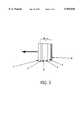
- FIG. 3shows an embodiment of the invention with a mixed layer, an electron transporting layer, and a hole transporting layer.
- FIG. 4shows the current-voltage characteristic of Embodiment 1.
- FIG. 5shows the current-luminance characteristic of Embodiment 1.
- FIG. 6shows the emission spectrum of Embodiment 1.
- FIG. 7shows the current-voltage characteristic of Embodiment 2.
- FIG. 8shows the current-luminance characteristic of Embodiment 2.
- FIG. 9shows the emission spectrum of Embodiment 2.
- FIG. 10shows the absorption spectrum of an exciplex compared with the absorption spectra of the basic compounds.
- the organic electroluminescent component according to the inventionin its simplest embodiment comprises a substrate layer 1, a first transparent electrode layer 2, a mixed layer 3, and a second electrode 4.
- an electron transporting layer 5is present between the mixed layer 3 and the second electrode 4.
- a further embodiment, shown in FIG. 3,comprises three separate layers which are optoelectronically active: a hole transporting layer 6, a mixed layer 3, and an electron transporting layer 5.
- a plate of a light-transmitting materialfor example a glass plate, always serves as the substrate 1.
- a thin film of a few 100 nm thicknessis provided thereon as the anode 2, which should also be light-transmitting.
- the hole transporting layerhaving a layer thickness of 100 nm to 2000 nm, preferably 500 nm
- the mixed layerwith a layer thickness of 100 nm to 2000 nm, preferably 200 nm
- the organic electroluminescent componentis completed with the cathode 4.
- Metals, metal oxides, or electrically conductive organic polymers having a high work function for electronsare suitable for use as the material for the transparent anode from which holes are injected into the p-type conducting layer.
- Examplesare thin, transparent layers of indium-doped tin oxide (ITO), gold, and polyaniline.
- Combinations of hole transporting and electron transporting compounds, which form exciplexes,are used for the mixed layer. These are, for example, combinations of 4,4',4"-tris(3-methylphenylphenylamino)-triphenylamine (MTDATA) or N,N'-di(4-methylphenyl)-N,N'-diphenyl-1,4-phenylenediamine (DPPD) with 2-(4-biphenylyl)-5-(tert.-butylphenyl)-1,3,4-oxadiazole (butyl-PBD), 2-(4-biphenylyl)-5-phenyl-1,3,4-oxadiazole (PBD), or 5-(4-biphenylyl)-3-tert.-butylphenyl)-1,2,4-triazole (TAZ).
- MTDATA4,4',4"-tris(3-methylphenylphenylamino)-triphenylamine
- DPPD
- conductive triphenylamine derivativesare used for the hole transporting layer which is in contact with the anode and the mixed layer, such as 4,4',4"-tris(3-methylphenylphenylamino)-triphenylamine (MTDATA), N,N'-diphenyl-N,N'-bis(3-methylphenyl)-1,1'-biphenyl-4,4'-diamine (TPD), N,N'-di(4-methylphenyl)-N,N'-diphenyl-1,4-phenylenediamine (DPPD), or 1,1'-bis-(4'-bis-(4'-methylphenyl)-aminophenyl)-cyclohexane (TDAPC).
- MTDATA4,4',4"-tris(3-methylphenylphenylamino)-triphenylamine
- TPDN,N'-diphenyl-N,N'-bis(3-methylphenyl)-1,1
- the electron transporting layerwhich is in contact with the cathode and with the mixed layer
- the followingare preferably used: 2-(4-biphenylyl)-5-(tert.-butylphenyl)-1,3,4-oxadiazole (butyl-PBD), 2-(4-biphenylyl)-5-phenyl-1,3,4-oxadiazole (PBD), or 5-(4-biphenylyl)-3-(tert.-butylphenyl)-1,2,4-triazole (TAZ).
- Metals with a low work functionare used as materials for the cathode because electrons are to be injected into the electron transporting layer from the cathode.
- Such metalsare aluminum, magnesium, and alloys of magnesium with silver or indium, and calcium, alkali metals such as Li, Na, K, Cs, or rare earth metals such as europium or terbium.
- the electron transporting or hole transporting materialsmay be provided from a solution, vapor-deposited in high vacuum, sublimated, or polymerized in situ for manufacturing the mixed layer.
- the hole transporting and the electron transporting compoundsare jointly deposited so that a homogeneous intermixing is achieved in the mixed layer.
- a DC voltageis applied to the two electrodes during operation.
- the first electrodewill then be at a positive potential (anode), the second at a negative potential (cathode).
- positive charge carriersi.e. holes
- Negative charge carriersi.e. electrons
- These charge carriersrecombine in the mixed layer and thus supply the excitation energy for the exciplex.
- the excitation energyis given off again in the form of radiation.
- the hole transporting and electron transporting compounds used in accordance with the inventionemit in the ultraviolet or blue spectrum range when used as single substances, but in the green or yellow spectrum range when combined into an exciplex.
- the combination of MTDATA and PBD or butyl-PBDin particular show a very strong green exciplex emission.
- Test samples having an emission surface of 0.5 cm diameterwere manufactured for finding the characteristics of the components, and the current-voltage curve, the current-luminance curve, and the emission spectrum are measured.
- FIG. 10shows the absorption spectra of the single components MTDATA and butyl-PBD, the spectrum obtained through mathematical summing of those of MTDATA and butyl-PBD, and the spectrum of the combination of MTDATA and butyl-PBD.
- the summed spectrum and the spectrum of the combinationare identical. This renders it clear in conjunction with the emission spectra that a genuine exciplex formation obtains here, and not a charge transfer complex. Both the emission and the absorption are indicated in relative units.
- a glass plate with a layer of indium-doped tin oxide thereonis rinsed with a KOH/ethanol solution and subsequently with deionized water and ethanol for cleaning. It is dried and treated for 15 minutes in a UV ozonizer. Then the following layers are vapor-deposited in high vacuum at 5 ⁇ 10 -6 mbar: MTDATA as the hole transporting layer, layer thickness 250 nm, MTDATA and TAZ in a molar ratio of 1:1 as the mixed layer with a thickness of 600 nm, TAZ as the electron transporting layer with a layer thickness of 280 nm, Ca as the cathode with a layer thickness of 250 nm, and Al with a layer thickness of 880 nm.
- a luminance of 700 cd/m 2was found at a current of 50 mA/cm 2 when a voltage of 10 V was applied.
- the current-voltage characteristicis shown in FIG. 4, the current-luminance curve in FIG. 5, and the emission spectrum in FIG. 6.
- a glass plate with a layer of indium-doped tin oxide thereonis cleaned and pretreated as described with reference to Embodiment 1. Then the following layers are vapor-deposited in high vacuum at 5 ⁇ 10 -6 mbar: MTDATA as the hole transporting layer with a layer thickness of 200 nm, MTDATA and butyl-PBD in a molar ratio of 3:1 as the mixed layer with a layer thickness of 513 nm, TAZ as the electron transporting layer with a layer thickness of 290 nm, Ca as the cathode with a layer thickness of 250 nm, and Al with a layer thickness of 2000 nm.
- a luminance of 4200 cd/m 2was found at a current of 175 mA/cm 2 when a voltage of 11 V was applied.
- the current-voltage characteristicis shown in FIG. 7, the current-luminance curve in FIG. 8, and the emission spectrum in FIG. 9.
Landscapes
- Chemical & Material Sciences (AREA)
- Engineering & Computer Science (AREA)
- Materials Engineering (AREA)
- Organic Chemistry (AREA)
- Electroluminescent Light Sources (AREA)
- Luminescent Compositions (AREA)
Abstract
Description
The invention relates to an organic electroluminescent component with a transparent substrate, a first transparent electrode, an organic electroluminescent layer, and a second electrode.
Electroluminescent components built up from organic layers are of major importance because they can be manufactured in the form of large-area displays which can be operated at low voltages and which have a short response time and a low weight. They can also be manufactured in the form of flexible foils which are more widely applicable than traditional electroluminescent components made from inorganic semiconductor material. Fields of application for organic electroluminescent components accordingly are displays of all kinds, in particular also flat monitors and picture screens. The components are suitable for use as light sources in airplanes and spaceships because of their low weight. A further possibility is for these components to be used as laser diodes.
Traditional organic electroluminescent components usually have a layer structure comprising several separate layers. An organic electroluminescent component is known, for example, from U.S. Pat. No. 4,720,432 and comprises in that order an anode, an organic hole injecting and transporting zone, an organic electron injecting and transporting zone, and a cathode, and which is characterized in that the hole injecting and transporting zone comprises a layer which is in contact with the anode and which contains a hole injecting porphyrinic compound, and furthermore comprises a layer which contains a hole transporting aromatic tertiary amine and which lies between the hole injecting layer and the electron injecting and transporting zone.
Such multiple combinations of layers with charge injecting and charge transporting organic materials necessarily have many interfaces. The transition voltages at the interfaces lead to an undesirable increase in the operating voltage, a reduction in the current density, and a reduction in the brightness of the electroluminescent component.
It is accordingly an object of the present invention to provide an organic electroluminescent component which has a simple layer structure.
According to the invention, this object is achieved by means of an organic electroluminescent component with a transparent substrate, a first transparent electrode, an organic electroluminescent layer which is a mixed layer comprising a mixture of a hole transporting and an electron transporting organic material which forms an exciplex, and a second electrode.
Combinations of a hole transporting material and an electron transporting material which form a light-emitting exciplex are chosen for the mixed layer. The functions of hole transport, electron transport and light emission can thus be combined in a single layer which in the simplest embodiment is composed of no more than two different charge transporting compounds. The use of additional emitter compounds is dispensed with according to the invention. A simpler layer structure is thus achieved for the organic electroluminescent component, which is characterized by improved operational properties, in particular a low operating voltage and a high luminance at low voltage. The components have a long useful life because no further compounds are used besides the hole transporting and the electron transporting compounds, in which the redox processes serving for the charge transport are reversible. The components show no self-absorption and no absorption in the visible range of the spectrum.
It is preferred within the scope of the present invention that the mixture forming an exciplex comprises as the hole transporting material one or several compounds from thegroup
These compounds form exciplexes in pairs, i.e. electronically excited complexes are created through interaction between the two compounds in one addition compound, which complexes are dissociated in the ground state but have a weak chemical bond in the excited state. The emission spectrum is changed by the exciplex formation. The emission lines of the individual compounds disappear and a broad, characteristic emission arises which is shifted into the low-frequency range compared with the individual components.
It is particularly preferred within the scope of the present invention that the hole transporting material is 4,4',4"-tris(3-methylphenylphenylamino)-triphenylamine (MTDATA) and the electron transporting material is 5-(4-biphenylyl)-3-(tert.-butylphenyl)-1,2,4-triazole (TAZ).
Another embodiment of the invention is characterized in that a layer of a hole transporting organic material is arranged between the first electrode and the mixed layer.
A further embodiment of the invention is characterized in that a layer of an electron transporting organic material is arranged between the second electrode and the mixed layer.
A particularly preferred embodiment of the invention is characterized in that a layer of a hole transporting organic material is arranged between the first electrode and the mixed layer, and a layer of an electron transporting organic material is arranged between the second electrode and the mixed layer.
The arrangement of the mixed layer between purely hole transporting and/or electron transporting substances prevents a throughput of the charge carriers via the electrodes without radiation generation. An improved recombination of the charge carriers and a higher luminous efficacy are thus achieved.
The invention will be explained in more detail below with reference to ten Figures.
FIG. 1 shows an embodiment of the invention with a single mixed layer.
FIG. 2 shows an embodiment of the invention with a mixed layer and an electron transporting layer.
FIG. 3 shows an embodiment of the invention with a mixed layer, an electron transporting layer, and a hole transporting layer.
FIG. 4 shows the current-voltage characteristic ofEmbodiment 1.
FIG. 5 shows the current-luminance characteristic ofEmbodiment 1.
FIG. 6 shows the emission spectrum ofEmbodiment 1.
FIG. 7 shows the current-voltage characteristic ofEmbodiment 2.
FIG. 8 shows the current-luminance characteristic ofEmbodiment 2.
FIG. 9 shows the emission spectrum ofEmbodiment 2.
FIG. 10 shows the absorption spectrum of an exciplex compared with the absorption spectra of the basic compounds.
The organic electroluminescent component according to the invention in its simplest embodiment comprises asubstrate layer 1, a firsttransparent electrode layer 2, a mixedlayer 3, and asecond electrode 4.
In another embodiment, shown in FIG. 2, anelectron transporting layer 5 is present between themixed layer 3 and thesecond electrode 4.
A further embodiment, shown in FIG. 3, comprises three separate layers which are optoelectronically active: ahole transporting layer 6, a mixedlayer 3, and anelectron transporting layer 5.
A plate of a light-transmitting material, for example a glass plate, always serves as thesubstrate 1. A thin film of a few 100 nm thickness is provided thereon as theanode 2, which should also be light-transmitting. This is followed by, if applicable, the hole transporting layer having a layer thickness of 100 nm to 2000 nm, preferably 500 nm, the mixed layer with a layer thickness of 100 nm to 2000 nm, preferably 200 nm, and possibly the electron transporting layer with a layer thickness of 100 nm to 2000 nm, preferably 500 nm.
The organic electroluminescent component is completed with thecathode 4.
Metals, metal oxides, or electrically conductive organic polymers having a high work function for electrons are suitable for use as the material for the transparent anode from which holes are injected into the p-type conducting layer. Examples are thin, transparent layers of indium-doped tin oxide (ITO), gold, and polyaniline.
Combinations of hole transporting and electron transporting compounds, which form exciplexes, are used for the mixed layer. These are, for example, combinations of 4,4',4"-tris(3-methylphenylphenylamino)-triphenylamine (MTDATA) or N,N'-di(4-methylphenyl)-N,N'-diphenyl-1,4-phenylenediamine (DPPD) with 2-(4-biphenylyl)-5-(tert.-butylphenyl)-1,3,4-oxadiazole (butyl-PBD), 2-(4-biphenylyl)-5-phenyl-1,3,4-oxadiazole (PBD), or 5-(4-biphenylyl)-3-tert.-butylphenyl)-1,2,4-triazole (TAZ). The combination of MTDATA with PBD or butyl-PBD is preferred.
Preferably, conductive triphenylamine derivatives are used for the hole transporting layer which is in contact with the anode and the mixed layer, such as 4,4',4"-tris(3-methylphenylphenylamino)-triphenylamine (MTDATA), N,N'-diphenyl-N,N'-bis(3-methylphenyl)-1,1'-biphenyl-4,4'-diamine (TPD), N,N'-di(4-methylphenyl)-N,N'-diphenyl-1,4-phenylenediamine (DPPD), or 1,1'-bis-(4'-bis-(4'-methylphenyl)-aminophenyl)-cyclohexane (TDAPC).
For the electron transporting layer which is in contact with the cathode and with the mixed layer, the following are preferably used: 2-(4-biphenylyl)-5-(tert.-butylphenyl)-1,3,4-oxadiazole (butyl-PBD), 2-(4-biphenylyl)-5-phenyl-1,3,4-oxadiazole (PBD), or 5-(4-biphenylyl)-3-(tert.-butylphenyl)-1,2,4-triazole (TAZ).
Metals with a low work function are used as materials for the cathode because electrons are to be injected into the electron transporting layer from the cathode. Such metals are aluminum, magnesium, and alloys of magnesium with silver or indium, and calcium, alkali metals such as Li, Na, K, Cs, or rare earth metals such as europium or terbium.
The electron transporting or hole transporting materials may be provided from a solution, vapor-deposited in high vacuum, sublimated, or polymerized in situ for manufacturing the mixed layer. The hole transporting and the electron transporting compounds are jointly deposited so that a homogeneous intermixing is achieved in the mixed layer.
A DC voltage is applied to the two electrodes during operation. The first electrode will then be at a positive potential (anode), the second at a negative potential (cathode). When the voltage present across the mixed layer has exceeded a threshold value, positive charge carriers, i.e. holes, are injected from the anode into the material forming the exciplex. Negative charge carriers, i.e. electrons, are injected from the cathode. These charge carriers recombine in the mixed layer and thus supply the excitation energy for the exciplex. The excitation energy is given off again in the form of radiation. The hole transporting and electron transporting compounds used in accordance with the invention emit in the ultraviolet or blue spectrum range when used as single substances, but in the green or yellow spectrum range when combined into an exciplex. The combination of MTDATA and PBD or butyl-PBD in particular show a very strong green exciplex emission.
Test samples having an emission surface of 0.5 cm diameter were manufactured for finding the characteristics of the components, and the current-voltage curve, the current-luminance curve, and the emission spectrum are measured.
To measure the absorption spectrum, solutions of the combination of MTDATA with butyl-PBD according to the invention and solutions of the two basic compounds in polymethacrylic-acid-methylester are provided in a spin-coating process on a quartz glass substrate for measuring the absorption spectrum. FIG. 10 shows the absorption spectra of the single components MTDATA and butyl-PBD, the spectrum obtained through mathematical summing of those of MTDATA and butyl-PBD, and the spectrum of the combination of MTDATA and butyl-PBD. The summed spectrum and the spectrum of the combination are identical. This renders it clear in conjunction with the emission spectra that a genuine exciplex formation obtains here, and not a charge transfer complex. Both the emission and the absorption are indicated in relative units.
A glass plate with a layer of indium-doped tin oxide thereon is rinsed with a KOH/ethanol solution and subsequently with deionized water and ethanol for cleaning. It is dried and treated for 15 minutes in a UV ozonizer. Then the following layers are vapor-deposited in high vacuum at 5×10⁻⁶ mbar: MTDATA as the hole transporting layer,layer thickness 250 nm, MTDATA and TAZ in a molar ratio of 1:1 as the mixed layer with a thickness of 600 nm, TAZ as the electron transporting layer with a layer thickness of 280 nm, Ca as the cathode with a layer thickness of 250 nm, and Al with a layer thickness of 880 nm.
A luminance of 700 cd/m2 was found at a current of 50 mA/cm2 when a voltage of 10 V was applied. The current-voltage characteristic is shown in FIG. 4, the current-luminance curve in FIG. 5, and the emission spectrum in FIG. 6.
A glass plate with a layer of indium-doped tin oxide thereon is cleaned and pretreated as described with reference toEmbodiment 1. Then the following layers are vapor-deposited in high vacuum at 5×10⁻⁶ mbar: MTDATA as the hole transporting layer with a layer thickness of 200 nm, MTDATA and butyl-PBD in a molar ratio of 3:1 as the mixed layer with a layer thickness of 513 nm, TAZ as the electron transporting layer with a layer thickness of 290 nm, Ca as the cathode with a layer thickness of 250 nm, and Al with a layer thickness of 2000 nm.
A luminance of 4200 cd/m2 was found at a current of 175 mA/cm2 when a voltage of 11 V was applied. The current-voltage characteristic is shown in FIG. 7, the current-luminance curve in FIG. 8, and the emission spectrum in FIG. 9.
Claims (10)
1. A organic electroluminescent component with a transparent substrate, a first transparent electrode, an organic electroluminescent layer which is a mixed layer comprising a mixture of a hole transporting and an electron transporting organic material which forms an exciplex, and a second electrode,
wherein the mixture forming an exciplex comprises as the hole transporting material one or several compounds from the group 4,4',4"-tris(3-methylphenylphenylamino)-triphenyl amine (MTDATA), N,N'-diphenyl-N,N'-bis(3-methylphenyl)-1,1'-biphenyl-4,4'-diamine (TPD), N,N'-di(4-methylphenyl)-N,N'-diphenyl-1,4-phenylenediamine (DPPD), and 1,1'-bis-(4'-bis-(4'-methylphenyl)-aminophenyl)-cyclohexane (TDAPC), and as the electron transporting material one or several compounds from the group 2-(4-biphenylyl)-5-(tert.-butylphenyl)-1,3,4-oxadiazole (butyl-PBD), 2-(4-biphenylyl)-5-phenyl-1,3,4-oxadiazole (PBD), and 5-(4-biphenylyl)-3-(tert.-butylphenyl)-1,2,4-triazole (TAZ).
2. An organic electroluminescent component as claimed in claim 1, wherein the hole transporting material is 4,4',4"-tris(3-methylphenylphenylamino)-triphenylamine (MTDATA) and the electron transporting material is 5-(4-biphenylyl)-3-(tert.-butylphenyl)-1,2,4-triazole (TAZ).
3. An organic electroluminescent component as claimed in claim 1, wherein a layer of a hole transporting organic material is arranged between the first electrode and the mixed layer.
4. An organic electroluminescent component as claimed in claim 1, wherein a layer of an electron transporting organic material is arranged between the second electrode and the mixed layer.
5. An organic electroluminescent component as claimed in claim 1, wherein a layer of a hole transporting organic material is arranged between the first electrode and the mixed layer, and a layer of an electron transporting organic material is arranged between the second electrode and the mixed layer.
6. An organic electroluminescent component as claimed in claim 1, wherein the hole transporting material is 4,4',4"-tris(3-methylphenylphenylamino)-triphenylamine (MTDATA) and the electron transporting material is 2-(4-biphenylyl)-5-(tert.-butylphenyl)-1,3,4-oxadiazole (butyl-PBD), 2-(4-biphenylyl)-5-phenyl-1,3,4-oxadiazole (PBD).
7. An organic electroluminescent component with a transparent substrate; a first transparent electrode; as a hole transporting layer 4,4',4"-tris(3-methylphenylphenylamino)-triphenylamine (MTDATA); an organic electroluminescent layer which is a mixed layer comprising a mixture of 4,4',4"-tris(3-methylphenylphenylamino)-triphenylamine (MTDATA) and 5-(4-biphenylyl)-3-(tert.-butylphenyl)-1,2,4-triazole (TAZ) which forms an exciplex; as an electron transporting layer 5-(4-biphenylyl)-3-(tert.-butylphenyl)-1,2,4-triazole (TAZ); and a second electrode.
8. An organic electroluminescent component with a transparent substrate; a first transparent electrode; as a hole transporting layer 4,4',4"-tris(3-methylphenylphenylamino)-triphenylamine (MTDATA); an organic electroluminescent layer which is a mixed layer comprising a mixture of 4,4',4"-tris(3-methylphenylphenylamino)-triphenylamine (MTDATA) and 2-(4-biphenylyl)-5-(tert.-butylphenyl)-1,3,4-oxadiazole (butyl-PBD) which forms an exciplex; as an electron transporting layer 5-(4-biphenylyl)-3-(tert.-butylphenyl)-1,2,4-triazole (TAZ); and a second electrode.
9. An organic electroluminescent component as claimed in claim 7, wherein the first electrode is an Indium-doped tin oxide.
10. An organic electroluminescent component as claimed in claim 8, wherein the first electrode is an Indium-doped tin oxide.
Applications Claiming Priority (2)
| Application Number | Priority Date | Filing Date | Title |
|---|---|---|---|
| DE19638770ADE19638770A1 (en) | 1996-09-21 | 1996-09-21 | Organic electroluminescent device with Exciplex |
| DE19638770 | 1996-09-21 |
Publications (1)
| Publication Number | Publication Date |
|---|---|
| US5955836Atrue US5955836A (en) | 1999-09-21 |
Family
ID=7806466
Family Applications (1)
| Application Number | Title | Priority Date | Filing Date |
|---|---|---|---|
| US08/933,292Expired - Fee RelatedUS5955836A (en) | 1996-09-21 | 1997-09-18 | Organic electroluminescent component with exciplex formed from a mixed layer of a mixture of hole transporting and electron transporting organic material |
Country Status (4)
| Country | Link |
|---|---|
| US (1) | US5955836A (en) |
| EP (1) | EP0831676B1 (en) |
| JP (1) | JPH10106748A (en) |
| DE (2) | DE19638770A1 (en) |
Cited By (51)
| Publication number | Priority date | Publication date | Assignee | Title |
|---|---|---|---|---|
| NL1015215C2 (en)* | 2000-05-17 | 2001-11-20 | Paul Robert Duynstee | Ultraviolet scanner to check authenticity of banknotes, is small enough to carry in purse or handbag |
| US20010051207A1 (en)* | 2000-05-12 | 2001-12-13 | Hirokazu Yamagata | Method of manufacturing a light emitting device |
| US6392339B1 (en)* | 1999-07-20 | 2002-05-21 | Xerox Corporation | Organic light emitting devices including mixed region |
| US20020074935A1 (en)* | 2000-12-15 | 2002-06-20 | Kwong Raymond C. | Highly stable and efficient OLEDs with a phosphorescent-doped mixed layer architecture |
| US20020086180A1 (en)* | 2000-12-28 | 2002-07-04 | Satoshi Seo | Luminescent device |
| US20020093283A1 (en)* | 2001-01-17 | 2002-07-18 | Satoshi Seo | Luminescent device and method of manufacturing same |
| US20020101154A1 (en)* | 2001-02-01 | 2002-08-01 | Satoshi Seo | Organic light emitting element and display device using the element |
| US20020105005A1 (en)* | 2001-02-08 | 2002-08-08 | Satoshi Seo | Light emitting device |
| US20020109136A1 (en)* | 2001-01-18 | 2002-08-15 | Satoshi Seo | Light emitting device and manufacturing method thereof |
| US20020113546A1 (en)* | 2001-02-22 | 2002-08-22 | Satoshi Seo | Organic light emitting device and display device using the same |
| US20020121860A1 (en)* | 2000-12-28 | 2002-09-05 | Satoshi Seo | Light emitting device and method of manufacturing the same |
| US20020139303A1 (en)* | 2001-02-01 | 2002-10-03 | Shunpei Yamazaki | Deposition apparatus and deposition method |
| US20020155632A1 (en)* | 2001-02-21 | 2002-10-24 | Shunpei Yamazaki | Method and apparatus for film deposition |
| US6528942B1 (en)* | 1999-07-13 | 2003-03-04 | Rohm Co., Ltd. | Organic electroluminescence device, its manufacturing method and board for display device used therefor |
| US6723445B2 (en) | 2001-12-31 | 2004-04-20 | Canon Kabushiki Kaisha | Organic light-emitting devices |
| US20040154542A1 (en)* | 2001-02-08 | 2004-08-12 | Semiconductor Energy Laboratory Co., Ltd., A Japan Corporation | Film formation apparatus and film formation method |
| US20040264046A1 (en)* | 2003-06-25 | 2004-12-30 | Hitachi Global Storage Technologies | Magnetic head with thinned T-shaped write pole and its fabrication |
| WO2004099338A3 (en)* | 2002-09-25 | 2005-01-06 | 3M Innovative Properties Co | Organic electroluminescent compositions |
| US20050048317A1 (en)* | 2003-08-29 | 2005-03-03 | Semiconductor Energy Laboratory Co., Ltd. | Electroluminescent device and light-emitting device including the same |
| US20050048310A1 (en)* | 2001-07-13 | 2005-03-03 | Consiglio Nazionale Delle Ricerche | Organic electroluminescent device based upon emission of exciplexes or electroplexes, and a method for its fabrication |
| US20050185794A1 (en)* | 2002-05-10 | 2005-08-25 | Harris Corporation | Secure wireless local or metropolitan area network and related methods |
| US20050221116A1 (en)* | 2002-03-29 | 2005-10-06 | Massimo Cocchi | Organic electroluminescent device with chromophore dopants |
| EP1227527A3 (en)* | 2001-01-26 | 2006-06-07 | LG. Philips LCD Co., Ltd. | Organic light emitting devices |
| US20060139893A1 (en)* | 2004-05-20 | 2006-06-29 | Atsushi Yoshimura | Stacked electronic component and manufacturing method thereof |
| US20060251919A1 (en)* | 2005-05-04 | 2006-11-09 | Xerox Corporation | Organic light emitting devices |
| US20060251920A1 (en)* | 2005-05-04 | 2006-11-09 | Xerox Corporation | Organic light emitting devices comprising a doped triazine electron transport layer |
| US20060261731A1 (en)* | 2005-05-20 | 2006-11-23 | Xerox Corporation | Stacked oled structure |
| US20060263593A1 (en)* | 2005-05-20 | 2006-11-23 | Xerox Corporation | Display devices with light absorbing metal nonoparticle layers |
| US20060263628A1 (en)* | 2005-05-20 | 2006-11-23 | Xerox Corporation | Display device with metal-organic mixed layer anodes |
| EP1311009A3 (en)* | 2001-11-08 | 2006-12-06 | LG. Philips LCD Co., Ltd. | Organic light emitting devices |
| US20070166568A1 (en)* | 2004-05-04 | 2007-07-19 | Koninklijke Philips Electronics, N.V. | Electroluminescent compounds containing exciton conducting compound |
| US7728517B2 (en) | 2005-05-20 | 2010-06-01 | Lg Display Co., Ltd. | Intermediate electrodes for stacked OLEDs |
| US7795806B2 (en) | 2005-05-20 | 2010-09-14 | Lg Display Co., Ltd. | Reduced reflectance display devices containing a thin-layer metal-organic mixed layer (MOML) |
| US20110240984A1 (en)* | 2008-12-12 | 2011-10-06 | Universal Display Corporation | Oled stability via doped hole transport layer |
| US20120217869A1 (en)* | 2011-02-28 | 2012-08-30 | Kyushu University National University Corporation | Delayed fluorescence material and organic electroluminescence device |
| US20140034932A1 (en)* | 2012-08-03 | 2014-02-06 | Semiconductor Energy Laboratory Co., Ltd. | Light-Emitting Element, Light-Emitting Device, Electronic Device, and Lighting Device |
| US8835911B2 (en) | 2011-03-04 | 2014-09-16 | Seiko Epson Corporation | Light emitting element, light emitting device, display, and electronic device |
| US8916854B2 (en) | 2011-03-04 | 2014-12-23 | Seiko Epson Corporation | Light-emitting element, light-emitting device, display device, and electronic apparatus |
| US20150303392A1 (en)* | 2014-04-18 | 2015-10-22 | Semiconductor Energy Laboratory Co., Ltd. | Light-emitting element, light-emitting device, electronic device, and lighting device |
| US9508949B2 (en) | 2012-07-18 | 2016-11-29 | Lg Display Co., Ltd. | Organic light-emitting device |
| US9559313B2 (en) | 2012-08-03 | 2017-01-31 | Semiconductor Energy Laboratory Co., Ltd. | Light-emitting element |
| US9604928B2 (en) | 2011-02-16 | 2017-03-28 | Semiconductor Energy Laboratory Co., Ltd. | Light-emitting element |
| US10240085B2 (en) | 2015-08-27 | 2019-03-26 | Samsung Electronics Co., Ltd. | Thin film and organic light-emitting device including the same |
| US10297764B2 (en) | 2015-09-14 | 2019-05-21 | Samsung Electronics Co., Ltd. | Mixture, thin film, and organic light emitting device including mixture and thin film |
| US10418575B2 (en)* | 2017-05-03 | 2019-09-17 | Wuhan China Star Optoelectronics Technology Co., Ltd. | OLED with mixed layer between the hole transport and emission layers |
| US10505120B2 (en) | 2011-02-28 | 2019-12-10 | Semiconductor Energy Laboratory Co., Ltd. | Light-emitting device |
| US20200274087A1 (en)* | 2019-02-22 | 2020-08-27 | Samsung Display Co., Ltd. | Organic light-emitting device |
| US10818861B2 (en) | 2012-04-13 | 2020-10-27 | Semiconductor Energy Laboratory Co., Ltd. | Light-emitting element, light-emitting device, electronic device, and lighting device |
| US10923664B2 (en) | 2015-09-14 | 2021-02-16 | Samsung Electronics Co., Ltd. | Composition, thin film, and organic light emitting device including composition and thin film |
| US11152583B2 (en)* | 2012-04-10 | 2021-10-19 | Samsung Electronics Co., Ltd | Organic light-emitting diode containing co-hosts forming exciplex, and lighting device and display apparatus including same |
| TWI892393B (en) | 2011-02-28 | 2025-08-01 | 日商半導體能源研究所股份有限公司 | Light-emitting element |
Families Citing this family (8)
| Publication number | Priority date | Publication date | Assignee | Title |
|---|---|---|---|---|
| JP2000133453A (en)* | 1998-10-22 | 2000-05-12 | Idemitsu Kosan Co Ltd | Organic electroluminescence device and method of manufacturing the same |
| CN1082782C (en)* | 1999-09-21 | 2002-04-10 | 光磊科技股份有限公司 | Organic light-emitting element and method for manufacturing the same |
| US6863997B2 (en)* | 2001-12-28 | 2005-03-08 | The Trustees Of Princeton University | White light emitting OLEDs from combined monomer and aggregate emission |
| CN102349172B (en)* | 2009-03-13 | 2016-03-16 | 三菱化学株式会社 | Manufacturing method of organic electroluminescent element, organic electroluminescent element, organic EL display, and organic EL lighting |
| DE112012001504B4 (en)* | 2011-03-30 | 2017-09-21 | Semiconductor Energy Laboratory Co., Ltd. | Light-emitting element |
| JP6468689B2 (en)* | 2012-04-13 | 2019-02-13 | 株式会社半導体エネルギー研究所 | LIGHT EMITTING ELEMENT, LIGHT EMITTING DEVICE, ELECTRONIC DEVICE, AND LIGHTING DEVICE |
| JP6386136B2 (en)* | 2012-04-13 | 2018-09-05 | 株式会社半導体エネルギー研究所 | LIGHT EMITTING ELEMENT, LIGHT EMITTING DEVICE, ELECTRONIC DEVICE, AND LIGHTING DEVICE |
| KR101944483B1 (en)* | 2013-12-26 | 2019-01-31 | 엘지디스플레이 주식회사 | Organic light emitting device |
Citations (4)
| Publication number | Priority date | Publication date | Assignee | Title |
|---|---|---|---|---|
| US4720432A (en)* | 1987-02-11 | 1988-01-19 | Eastman Kodak Company | Electroluminescent device with organic luminescent medium |
| US5281489A (en)* | 1990-03-16 | 1994-01-25 | Asashi Kasei Kogyo Kabushiki Kaisha | Electroluminescent element |
| JPH0785972A (en)* | 1993-09-20 | 1995-03-31 | Toshiba Corp | Organic EL element |
| US5716722A (en)* | 1995-01-24 | 1998-02-10 | Sanyo Electric Co., Ltd. | Organic electrolluminescent device |
Family Cites Families (4)
| Publication number | Priority date | Publication date | Assignee | Title |
|---|---|---|---|---|
| US5420288A (en)* | 1992-04-14 | 1995-05-30 | Ricoh Company, Ltd. | Electroluminescent device comprising oxadiazole compounds luminescent material, oxadiazole compounds for the device, and method of producing oxadiazole compounds |
| JP2917795B2 (en)* | 1994-02-04 | 1999-07-12 | 住友電気工業株式会社 | Organic electroluminescence device and method of manufacturing the same |
| US5792567A (en)* | 1994-03-16 | 1998-08-11 | Sumitomo Electric Industries, Ltd. | Triazole derivatives and organic electroluminescent devices produced therefrom |
| DE69530654T2 (en)* | 1994-05-26 | 2004-03-11 | Sumitomo Electric Industries, Ltd. | ORGANIC ELECTROLUMINICENT ELEMENTS |
- 1996
- 1996-09-21DEDE19638770Apatent/DE19638770A1/ennot_activeWithdrawn
- 1997
- 1997-09-15EPEP97202820Apatent/EP0831676B1/ennot_activeExpired - Lifetime
- 1997-09-15DEDE59711176Tpatent/DE59711176D1/ennot_activeExpired - Fee Related
- 1997-09-18USUS08/933,292patent/US5955836A/ennot_activeExpired - Fee Related
- 1997-09-22JPJP9256865Apatent/JPH10106748A/ennot_activeAbandoned
Patent Citations (4)
| Publication number | Priority date | Publication date | Assignee | Title |
|---|---|---|---|---|
| US4720432A (en)* | 1987-02-11 | 1988-01-19 | Eastman Kodak Company | Electroluminescent device with organic luminescent medium |
| US5281489A (en)* | 1990-03-16 | 1994-01-25 | Asashi Kasei Kogyo Kabushiki Kaisha | Electroluminescent element |
| JPH0785972A (en)* | 1993-09-20 | 1995-03-31 | Toshiba Corp | Organic EL element |
| US5716722A (en)* | 1995-01-24 | 1998-02-10 | Sanyo Electric Co., Ltd. | Organic electrolluminescent device |
Non-Patent Citations (4)
| Title |
|---|
| "Electroluminescence of Molecularly-Doped Polymer Films Using Coumarin Derivative as an Emissive Center", Ching-Piao Lin, Tetsuo Tsutsui and Shogo Saito, Journal of Polymer Research vol. 2, No. 3 133-138, Jul. 1995. |
| Electroluminescence of Molecularly Doped Polymer Films Using Coumarin Derivative as an Emissive Center , Ching Piao Lin, Tetsuo Tsutsui and Shogo Saito, Journal of Polymer Research vol. 2, No. 3 133 138, Jul. 1995.* |
| Polymer Light Emitting Diodes with Single and Double Layer Structures Using Poly (2, 3 Diphenylquinoxaline 5, 8 Diyl), Takakazu Yamamoto, Tetsuji Inoue and Takaki Kanbara, Japanese Journal of Applied Physics, Part 2 (Letters), Feb. 15, 1994, pp. 250 253.* |
| Polymer Light-Emitting Diodes with Single-and Double-Layer Structures Using Poly (2, 3-Diphenylquinoxaline-5, 8-Diyl), Takakazu Yamamoto, Tetsuji Inoue and Takaki Kanbara, Japanese Journal of Applied Physics, Part 2 (Letters), Feb. 15, 1994, pp. 250-253. |
Cited By (133)
| Publication number | Priority date | Publication date | Assignee | Title |
|---|---|---|---|---|
| US6528942B1 (en)* | 1999-07-13 | 2003-03-04 | Rohm Co., Ltd. | Organic electroluminescence device, its manufacturing method and board for display device used therefor |
| US6392339B1 (en)* | 1999-07-20 | 2002-05-21 | Xerox Corporation | Organic light emitting devices including mixed region |
| US20010051207A1 (en)* | 2000-05-12 | 2001-12-13 | Hirokazu Yamagata | Method of manufacturing a light emitting device |
| NL1015215C2 (en)* | 2000-05-17 | 2001-11-20 | Paul Robert Duynstee | Ultraviolet scanner to check authenticity of banknotes, is small enough to carry in purse or handbag |
| US20020074935A1 (en)* | 2000-12-15 | 2002-06-20 | Kwong Raymond C. | Highly stable and efficient OLEDs with a phosphorescent-doped mixed layer architecture |
| US6803720B2 (en) | 2000-12-15 | 2004-10-12 | Universal Display Corporation | Highly stable and efficient OLEDs with a phosphorescent-doped mixed layer architecture |
| WO2002047457A3 (en)* | 2000-12-15 | 2003-07-24 | Universal Display Corp | Highly stable and efficient oleds with a phosphorescent-doped mixed layer architecture |
| US9209418B2 (en) | 2000-12-28 | 2015-12-08 | Semiconductor Energy Laboratory Co., Ltd. | Light emitting device and method of manufacturing the same |
| US7342355B2 (en) | 2000-12-28 | 2008-03-11 | Semiconductor Energy Laboratory Co., Ltd. | Light emitting device having organic light emitting material with mixed layer |
| US7915807B2 (en) | 2000-12-28 | 2011-03-29 | Semiconductor Energy Laboratory Co., Ltd. | Light emitting device and method of manufacturing the same |
| US20020121860A1 (en)* | 2000-12-28 | 2002-09-05 | Satoshi Seo | Light emitting device and method of manufacturing the same |
| US8878431B2 (en) | 2000-12-28 | 2014-11-04 | Semiconductor Energy Laboratory Co., Ltd. | Light emitting device and method of manufacturing the same |
| US20020086180A1 (en)* | 2000-12-28 | 2002-07-04 | Satoshi Seo | Luminescent device |
| US20110169400A1 (en)* | 2000-12-28 | 2011-07-14 | Semiconductor Energy Laboratory Co., Ltd. | Light Emitting Device and Method of Manufacturing the Same |
| US8432094B2 (en) | 2000-12-28 | 2013-04-30 | Semiconductor Energy Laboratory Co., Ltd. | Light emitting device and method of manufacturing the same |
| US7579089B2 (en) | 2000-12-28 | 2009-08-25 | Semiconductor Energy Laboratory Co., Ltd. | Luminescent device |
| US7572522B2 (en) | 2000-12-28 | 2009-08-11 | Semiconductor Energy Laboratory Co., Ltd. | Luminescent device |
| US20050260440A1 (en)* | 2000-12-28 | 2005-11-24 | Semiconductor Energy Laboratory Co., Ltd., A Japan Corporation | Luminescent device |
| US9362518B2 (en) | 2000-12-28 | 2016-06-07 | Semiconductor Energy Laboratory Co., Ltd. | Light emitting device and method of manufacturing the same |
| US20080111481A1 (en)* | 2000-12-28 | 2008-05-15 | Semiconductor Energy Laboratory Co., Ltd. | Light Emitting Device and Method of Manufacturing the Same |
| US8310147B2 (en) | 2000-12-28 | 2012-11-13 | Semiconductor Energy Laboratory Co., Ltd. | Luminescent device |
| US20050170737A1 (en)* | 2001-01-17 | 2005-08-04 | Semiconductor Energy Laboratory Co., Ltd., A Japan Corporation | Luminescent device and method of manufacturing same |
| US7550173B2 (en) | 2001-01-17 | 2009-06-23 | Semiconductor Energy Laboratory Co., Ltd. | Luminescent device and method of manufacturing same |
| US20020093283A1 (en)* | 2001-01-17 | 2002-07-18 | Satoshi Seo | Luminescent device and method of manufacturing same |
| US7332857B2 (en) | 2001-01-18 | 2008-02-19 | Semiconductor Energy Laboratory Co., Ltd. | Light emitting device and manufacturing method thereof |
| US20020109136A1 (en)* | 2001-01-18 | 2002-08-15 | Satoshi Seo | Light emitting device and manufacturing method thereof |
| EP1227527A3 (en)* | 2001-01-26 | 2006-06-07 | LG. Philips LCD Co., Ltd. | Organic light emitting devices |
| US9349977B2 (en) | 2001-02-01 | 2016-05-24 | Semiconductor Energy Laboratory Co., Ltd. | Light-emitting device having mixed layer including hole transporting compound |
| US7459722B2 (en) | 2001-02-01 | 2008-12-02 | Semiconductor Energy Laboratory Co., Ltd. | Organic light emitting element and display device using the element |
| US8354786B2 (en) | 2001-02-01 | 2013-01-15 | Semiconductor Energy Laboratory Co., Ltd. | Light-emitting device |
| US8174007B2 (en) | 2001-02-01 | 2012-05-08 | Semiconductor Energy Laboratory Co., Ltd. | Organic light emitting element and display device using the element |
| US20020101154A1 (en)* | 2001-02-01 | 2002-08-01 | Satoshi Seo | Organic light emitting element and display device using the element |
| US20110101322A1 (en)* | 2001-02-01 | 2011-05-05 | Semiconductor Energy Laboratory Co., Ltd. | Organic Light Emitting Element and Display Device Using the Element |
| SG118110A1 (en)* | 2001-02-01 | 2006-01-27 | Semiconductor Energy Lab | Organic light emitting element and display device using the element |
| US9608224B2 (en) | 2001-02-01 | 2017-03-28 | Semiconductor Energy Laboratory Co., Ltd. | Organic light emitting element and display device using the element |
| US7858977B2 (en) | 2001-02-01 | 2010-12-28 | Semiconductor Energy Laboratory Co., Ltd. | Organic light emitting element and display device using the element |
| US8674348B2 (en) | 2001-02-01 | 2014-03-18 | Semiconductor Energy Laboratory Co., Ltd. | Organic light emitting element and display device using the element |
| US20020139303A1 (en)* | 2001-02-01 | 2002-10-03 | Shunpei Yamazaki | Deposition apparatus and deposition method |
| US7173370B2 (en) | 2001-02-01 | 2007-02-06 | Semiconductor Energy Laboratory Co., Ltd. | Organic light emitting element and display device using the element |
| CN100481483C (en)* | 2001-02-01 | 2009-04-22 | 株式会社半导体能源研究所 | Organic light emitting element and display device using the same |
| US20090096369A1 (en)* | 2001-02-01 | 2009-04-16 | Semiconductor Energy Laboratory Co., Ltd. | Organic light emitting element and display device using the element |
| US9219241B2 (en) | 2001-02-01 | 2015-12-22 | Semiconductor Energy Laboratory Co., Ltd. | Organic light emitting element and display device using the element |
| US20070228362A1 (en)* | 2001-02-01 | 2007-10-04 | Semiconductor Energy Laboratory Co., Ltd. | Organic Light Emitting Element and Display Device Using the Element |
| US20090058285A1 (en)* | 2001-02-01 | 2009-03-05 | Semiconductor Energy Laboratory Co., Ltd. | Deposition Apparatus and Deposition Method |
| US7196360B2 (en) | 2001-02-08 | 2007-03-27 | Semiconductor Energy Laboratory Co., Ltd. | Light emitting device |
| US20040154542A1 (en)* | 2001-02-08 | 2004-08-12 | Semiconductor Energy Laboratory Co., Ltd., A Japan Corporation | Film formation apparatus and film formation method |
| US20060243970A1 (en)* | 2001-02-08 | 2006-11-02 | Semiconductor Energy Laboratory Co., Ltd. | Light Emitting Device |
| US20020105005A1 (en)* | 2001-02-08 | 2002-08-08 | Satoshi Seo | Light emitting device |
| US7456425B2 (en) | 2001-02-08 | 2008-11-25 | Semiconductor Energy Laboratory Co., Ltd. | Light emitting device |
| US8513648B2 (en) | 2001-02-08 | 2013-08-20 | Semiconductor Energy Laboratory Co., Ltd. | Light emitting device |
| US7629025B2 (en) | 2001-02-08 | 2009-12-08 | Semiconductor Energy Laboratory Co., Ltd. | Film formation apparatus and film formation method |
| US7432116B2 (en) | 2001-02-21 | 2008-10-07 | Semiconductor Energy Laboratory Co., Ltd. | Method and apparatus for film deposition |
| US20020155632A1 (en)* | 2001-02-21 | 2002-10-24 | Shunpei Yamazaki | Method and apparatus for film deposition |
| US20020113546A1 (en)* | 2001-02-22 | 2002-08-22 | Satoshi Seo | Organic light emitting device and display device using the same |
| SG118118A1 (en)* | 2001-02-22 | 2006-01-27 | Semiconductor Energy Lab | Organic light emitting device and display using the same |
| US7399991B2 (en) | 2001-02-22 | 2008-07-15 | Semiconductor Energy Laboratory Co., Ltd. | Organic light emitting device and display device using the same |
| US7663149B2 (en) | 2001-02-22 | 2010-02-16 | Semiconductor Energy Laboratory Co., Ltd. | Organic light emitting device and display device using the same |
| US20080197769A1 (en)* | 2001-02-22 | 2008-08-21 | Semiconductor Energy Laboratory Co., Ltd. | Organic light emitting device and display device using the same |
| US20050048310A1 (en)* | 2001-07-13 | 2005-03-03 | Consiglio Nazionale Delle Ricerche | Organic electroluminescent device based upon emission of exciplexes or electroplexes, and a method for its fabrication |
| EP1311009A3 (en)* | 2001-11-08 | 2006-12-06 | LG. Philips LCD Co., Ltd. | Organic light emitting devices |
| US6723445B2 (en) | 2001-12-31 | 2004-04-20 | Canon Kabushiki Kaisha | Organic light-emitting devices |
| US20050221116A1 (en)* | 2002-03-29 | 2005-10-06 | Massimo Cocchi | Organic electroluminescent device with chromophore dopants |
| US20050185794A1 (en)* | 2002-05-10 | 2005-08-25 | Harris Corporation | Secure wireless local or metropolitan area network and related methods |
| WO2004099338A3 (en)* | 2002-09-25 | 2005-01-06 | 3M Innovative Properties Co | Organic electroluminescent compositions |
| US20040264046A1 (en)* | 2003-06-25 | 2004-12-30 | Hitachi Global Storage Technologies | Magnetic head with thinned T-shaped write pole and its fabrication |
| US20050048317A1 (en)* | 2003-08-29 | 2005-03-03 | Semiconductor Energy Laboratory Co., Ltd. | Electroluminescent device and light-emitting device including the same |
| US7807276B2 (en)* | 2004-05-04 | 2010-10-05 | Koninklijke Philips Electronics N.V. | Electroluminescent compounds containing exciton conducting compound |
| US20070166568A1 (en)* | 2004-05-04 | 2007-07-19 | Koninklijke Philips Electronics, N.V. | Electroluminescent compounds containing exciton conducting compound |
| US20060139893A1 (en)* | 2004-05-20 | 2006-06-29 | Atsushi Yoshimura | Stacked electronic component and manufacturing method thereof |
| US20060251920A1 (en)* | 2005-05-04 | 2006-11-09 | Xerox Corporation | Organic light emitting devices comprising a doped triazine electron transport layer |
| US8487527B2 (en) | 2005-05-04 | 2013-07-16 | Lg Display Co., Ltd. | Organic light emitting devices |
| US7777407B2 (en) | 2005-05-04 | 2010-08-17 | Lg Display Co., Ltd. | Organic light emitting devices comprising a doped triazine electron transport layer |
| US20060251919A1 (en)* | 2005-05-04 | 2006-11-09 | Xerox Corporation | Organic light emitting devices |
| US20060261731A1 (en)* | 2005-05-20 | 2006-11-23 | Xerox Corporation | Stacked oled structure |
| US7750561B2 (en) | 2005-05-20 | 2010-07-06 | Lg Display Co., Ltd. | Stacked OLED structure |
| US20060263593A1 (en)* | 2005-05-20 | 2006-11-23 | Xerox Corporation | Display devices with light absorbing metal nonoparticle layers |
| US7943244B2 (en) | 2005-05-20 | 2011-05-17 | Lg Display Co., Ltd. | Display device with metal-organic mixed layer anodes |
| US7811679B2 (en) | 2005-05-20 | 2010-10-12 | Lg Display Co., Ltd. | Display devices with light absorbing metal nanoparticle layers |
| US20060263628A1 (en)* | 2005-05-20 | 2006-11-23 | Xerox Corporation | Display device with metal-organic mixed layer anodes |
| GB2426856A (en)* | 2005-05-20 | 2006-12-06 | Lg Philips Lcd Co Ltd | Stacked OLED structure having mixed region |
| US7795806B2 (en) | 2005-05-20 | 2010-09-14 | Lg Display Co., Ltd. | Reduced reflectance display devices containing a thin-layer metal-organic mixed layer (MOML) |
| GB2426856B (en)* | 2005-05-20 | 2007-08-01 | Lg Philips Lcd Co Ltd | Stacked oled structure |
| US7728517B2 (en) | 2005-05-20 | 2010-06-01 | Lg Display Co., Ltd. | Intermediate electrodes for stacked OLEDs |
| US8778511B2 (en)* | 2008-12-12 | 2014-07-15 | Universal Display Corporation | OLED stability via doped hole transport layer |
| US20110240984A1 (en)* | 2008-12-12 | 2011-10-06 | Universal Display Corporation | Oled stability via doped hole transport layer |
| US12100795B2 (en) | 2011-02-16 | 2024-09-24 | Semiconductor Energy Laboratory Co., Ltd. | Light-emitting element |
| US10573829B2 (en) | 2011-02-16 | 2020-02-25 | Semiconductor Energy Laboratory Co., Ltd. | Light-emitting element |
| US10586934B2 (en) | 2011-02-16 | 2020-03-10 | Semiconductor Energy Laboratory Co., Ltd. | Light-emitting element |
| US10593895B2 (en) | 2011-02-16 | 2020-03-17 | Semiconductor Energy Laboratory Co., Ltd. | Light-emitting element |
| US9604928B2 (en) | 2011-02-16 | 2017-03-28 | Semiconductor Energy Laboratory Co., Ltd. | Light-emitting element |
| US12108658B2 (en)* | 2011-02-28 | 2024-10-01 | Semiconductor Energy Laboratory Co., Ltd. | Light-emitting device |
| US11508912B2 (en) | 2011-02-28 | 2022-11-22 | Semiconductor Energy Laboratory Co., Ltd. | Light-emitting device |
| TWI831058B (en)* | 2011-02-28 | 2024-02-01 | 日商半導體能源研究所股份有限公司 | Light-emitting element |
| TWI892393B (en) | 2011-02-28 | 2025-08-01 | 日商半導體能源研究所股份有限公司 | Light-emitting element |
| US9783734B2 (en)* | 2011-02-28 | 2017-10-10 | Kyulux, Inc. | Delayed fluorescence material and organic electroluminescence device |
| TWI743606B (en)* | 2011-02-28 | 2021-10-21 | 日商半導體能源研究所股份有限公司 | Light-emitting element |
| US20120217869A1 (en)* | 2011-02-28 | 2012-08-30 | Kyushu University National University Corporation | Delayed fluorescence material and organic electroluminescence device |
| US10930852B2 (en) | 2011-02-28 | 2021-02-23 | Semiconductor Energy Laboratory Co., Ltd. | Light-emitting device |
| US10505120B2 (en) | 2011-02-28 | 2019-12-10 | Semiconductor Energy Laboratory Co., Ltd. | Light-emitting device |
| TWI680600B (en)* | 2011-02-28 | 2019-12-21 | 日商半導體能源研究所股份有限公司 | Light-emitting element |
| US8916854B2 (en) | 2011-03-04 | 2014-12-23 | Seiko Epson Corporation | Light-emitting element, light-emitting device, display device, and electronic apparatus |
| US8835911B2 (en) | 2011-03-04 | 2014-09-16 | Seiko Epson Corporation | Light emitting element, light emitting device, display, and electronic device |
| US11152583B2 (en)* | 2012-04-10 | 2021-10-19 | Samsung Electronics Co., Ltd | Organic light-emitting diode containing co-hosts forming exciplex, and lighting device and display apparatus including same |
| US11943945B2 (en) | 2012-04-10 | 2024-03-26 | Samsung Electronics Co., Ltd. | Organic light-emitting diode containing co-hosts forming exciplex, and lighting device and display apparatus including same |
| US10818861B2 (en) | 2012-04-13 | 2020-10-27 | Semiconductor Energy Laboratory Co., Ltd. | Light-emitting element, light-emitting device, electronic device, and lighting device |
| US11393997B2 (en) | 2012-04-13 | 2022-07-19 | Semiconductor Energy Laboratory Co., Ltd. | Light-emitting element, light-emitting device, electronic device, and lighting device |
| US9508949B2 (en) | 2012-07-18 | 2016-11-29 | Lg Display Co., Ltd. | Organic light-emitting device |
| TWI622198B (en)* | 2012-07-18 | 2018-04-21 | 樂金顯示科技股份有限公司 | Organic light emitting device |
| US10734594B2 (en) | 2012-08-03 | 2020-08-04 | Semiconductor Energy Laboratory Co., Ltd. | Light-emitting element |
| US10644254B2 (en) | 2012-08-03 | 2020-05-05 | Semiconductor Energy Laboratory Co., Ltd. | Light-emitting element |
| US10505132B2 (en) | 2012-08-03 | 2019-12-10 | Semiconductor Energy Laboratory Co., Ltd. | Light-emitting element |
| US20140034932A1 (en)* | 2012-08-03 | 2014-02-06 | Semiconductor Energy Laboratory Co., Ltd. | Light-Emitting Element, Light-Emitting Device, Electronic Device, and Lighting Device |
| US12262574B2 (en) | 2012-08-03 | 2025-03-25 | Semiconductor Energy Laboratory Co., Ltd. | Light-emitting element |
| CN108539032A (en)* | 2012-08-03 | 2018-09-14 | 株式会社半导体能源研究所 | Light-emitting component, light-emitting device, electronic equipment and lighting device |
| CN103579514A (en)* | 2012-08-03 | 2014-02-12 | 株式会社半导体能源研究所 | Light-emitting element, light-emitting device, electronic equipment, and lighting device |
| CN108321303A (en)* | 2012-08-03 | 2018-07-24 | 株式会社半导体能源研究所 | Light-emitting component, light-emitting device, electronic equipment and lighting device |
| US11730007B2 (en) | 2012-08-03 | 2023-08-15 | Semiconductor Energy Laboratory Co., Ltd. | Light-emitting element |
| DE102013214661B4 (en) | 2012-08-03 | 2023-01-05 | Semiconductor Energy Laboratory Co., Ltd. | Light-emitting element, light-emitting device and lighting device |
| US9947885B2 (en) | 2012-08-03 | 2018-04-17 | Semiconductor Energy Laboratory Co., Ltd. | Light-emitting element |
| US9559313B2 (en) | 2012-08-03 | 2017-01-31 | Semiconductor Energy Laboratory Co., Ltd. | Light-emitting element |
| US11355722B2 (en) | 2012-08-03 | 2022-06-07 | Semiconductor Energy Laboratory Co., Ltd. | Light-emitting element |
| CN108539032B (en)* | 2012-08-03 | 2020-02-21 | 株式会社半导体能源研究所 | Light-emitting element, light-emitting device, electronic equipment, and lighting device |
| US20150303392A1 (en)* | 2014-04-18 | 2015-10-22 | Semiconductor Energy Laboratory Co., Ltd. | Light-emitting element, light-emitting device, electronic device, and lighting device |
| US10240085B2 (en) | 2015-08-27 | 2019-03-26 | Samsung Electronics Co., Ltd. | Thin film and organic light-emitting device including the same |
| US11713416B2 (en) | 2015-08-27 | 2023-08-01 | Samsung Electronics Co., Ltd. | Thin film and organic light-emitting device including the same |
| US10995265B2 (en) | 2015-08-27 | 2021-05-04 | Samsung Electronics Co., Ltd. | Thin film and organic light-emitting device including the same |
| US10297764B2 (en) | 2015-09-14 | 2019-05-21 | Samsung Electronics Co., Ltd. | Mixture, thin film, and organic light emitting device including mixture and thin film |
| US10923664B2 (en) | 2015-09-14 | 2021-02-16 | Samsung Electronics Co., Ltd. | Composition, thin film, and organic light emitting device including composition and thin film |
| US10418575B2 (en)* | 2017-05-03 | 2019-09-17 | Wuhan China Star Optoelectronics Technology Co., Ltd. | OLED with mixed layer between the hole transport and emission layers |
| CN111613730B (en)* | 2019-02-22 | 2024-04-19 | 三星显示有限公司 | Organic light-emitting devices and electronic devices |
| US11158831B2 (en)* | 2019-02-22 | 2021-10-26 | Samsung Display Co., Ltd. | Organic light-emitting device |
| CN111613730A (en)* | 2019-02-22 | 2020-09-01 | 三星显示有限公司 | Organic Light Emitting Devices and Electronic Devices |
| US20200274087A1 (en)* | 2019-02-22 | 2020-08-27 | Samsung Display Co., Ltd. | Organic light-emitting device |
Also Published As
| Publication number | Publication date |
|---|---|
| EP0831676A3 (en) | 1998-07-15 |
| JPH10106748A (en) | 1998-04-24 |
| DE19638770A1 (en) | 1998-03-26 |
| DE59711176D1 (en) | 2004-02-12 |
| EP0831676A2 (en) | 1998-03-25 |
| EP0831676B1 (en) | 2004-01-07 |
Similar Documents
| Publication | Publication Date | Title |
|---|---|---|
| US5955836A (en) | Organic electroluminescent component with exciplex formed from a mixed layer of a mixture of hole transporting and electron transporting organic material | |
| JPH10106748A5 (en) | ||
| JP4153694B2 (en) | Organic EL device and display device | |
| Kido et al. | Single‐layer white light‐emitting organic electroluminescent devices based on dye‐dispersed poly (N‐vinylcarbazole) | |
| US6303238B1 (en) | OLEDs doped with phosphorescent compounds | |
| Kido et al. | Bright red light‐emitting organic electroluminescent devices having a europium complex as an emitter | |
| JP2773297B2 (en) | Organic thin film EL device | |
| JP2879080B2 (en) | EL device | |
| US6287712B1 (en) | Color-tunable organic light emitting devices | |
| JP2004319424A (en) | Organic electroluminescent display device | |
| JPH11149985A (en) | Organic electroluminescent device having inorganic electron transport layer | |
| EP1603369B1 (en) | Organic electroluminescence device and organic electroluminescence display | |
| Hosokawa et al. | Efficient electroluminescence of distyrylarylene with hole transporting ability | |
| JPH11111467A (en) | Organic electroluminescent device | |
| JP4669786B2 (en) | Display device | |
| JP4669785B2 (en) | Light emitting element and display device | |
| KR100547055B1 (en) | Organic electroluminescent devices | |
| JPH11102786A (en) | Organic electroluminescence element | |
| JPH07166160A (en) | Organic thin film EL device | |
| KR100581639B1 (en) | Organic Electroluminescent Device | |
| JPH11162647A (en) | Organic electroluminescence element | |
| KR100699966B1 (en) | Organic Electroluminescent Devices and Organic Electroluminescent Displays | |
| JPH06188073A (en) | Organic film element | |
| JP2003297550A (en) | Light emitting element, display device using the same, and lighting device | |
| JP2000268959A (en) | Method for changing emission color of organic EL element |
Legal Events
| Date | Code | Title | Description |
|---|---|---|---|
| AS | Assignment | Owner name:U.S. PHILIPS CORPORATION, NEW YORK Free format text:ASSIGNMENT OF ASSIGNORS INTEREST;ASSIGNORS:BOERNER, HERBERT;BUSSELT, WOLFGANG;JUSTEL, THOMAS;AND OTHERS;REEL/FRAME:009079/0393;SIGNING DATES FROM 19971017 TO 19971023 | |
| FPAY | Fee payment | Year of fee payment:4 | |
| REMI | Maintenance fee reminder mailed | ||
| LAPS | Lapse for failure to pay maintenance fees | ||
| STCH | Information on status: patent discontinuation | Free format text:PATENT EXPIRED DUE TO NONPAYMENT OF MAINTENANCE FEES UNDER 37 CFR 1.362 | |
| FP | Lapsed due to failure to pay maintenance fee | Effective date:20070921 |