US5955758A - Method of forming a capacitor plate and a capacitor incorporating same - Google Patents
Method of forming a capacitor plate and a capacitor incorporating sameDownload PDFInfo
- Publication number
- US5955758A US5955758AUS08/738,789US73878996AUS5955758AUS 5955758 AUS5955758 AUS 5955758AUS 73878996 AUS73878996 AUS 73878996AUS 5955758 AUS5955758 AUS 5955758A
- Authority
- US
- United States
- Prior art keywords
- layer
- capacitor
- electrically conductive
- electrically
- layers
- Prior art date
- Legal status (The legal status is an assumption and is not a legal conclusion. Google has not performed a legal analysis and makes no representation as to the accuracy of the status listed.)
- Expired - Lifetime
Links
- 239000003990capacitorSubstances0.000titleclaimsabstractdescription92
- 238000000034methodMethods0.000titleabstractdescription8
- 239000000463materialSubstances0.000claimsabstractdescription50
- 230000004888barrier functionEffects0.000claimsabstractdescription36
- 229910044991metal oxideInorganic materials0.000claimsabstractdescription29
- 150000004706metal oxidesChemical class0.000claimsabstractdescription29
- 238000010276constructionMethods0.000claimsabstractdescription10
- BASFCYQUMIYNBI-UHFFFAOYSA-NplatinumChemical compound[Pt]BASFCYQUMIYNBI-UHFFFAOYSA-N0.000claimsdescription27
- 229910021420polycrystalline siliconInorganic materials0.000claimsdescription27
- 229920005591polysiliconPolymers0.000claimsdescription27
- VYPSYNLAJGMNEJ-UHFFFAOYSA-NSilicium dioxideChemical compoundO=[Si]=OVYPSYNLAJGMNEJ-UHFFFAOYSA-N0.000claimsdescription24
- GWEVSGVZZGPLCZ-UHFFFAOYSA-NTitan oxideChemical compoundO=[Ti]=OGWEVSGVZZGPLCZ-UHFFFAOYSA-N0.000claimsdescription24
- 230000002093peripheral effectEffects0.000claimsdescription24
- WOCIAKWEIIZHES-UHFFFAOYSA-Nruthenium(iv) oxideChemical compoundO=[Ru]=OWOCIAKWEIIZHES-UHFFFAOYSA-N0.000claimsdescription20
- 238000009792diffusion processMethods0.000claimsdescription17
- 239000000203mixtureSubstances0.000claimsdescription17
- 229910052697platinumInorganic materials0.000claimsdescription14
- 229910018404Al2 O3Inorganic materials0.000claimsdescription12
- ATJFFYVFTNAWJD-UHFFFAOYSA-NTinChemical compound[Sn]ATJFFYVFTNAWJD-UHFFFAOYSA-N0.000claimsdescription12
- 229910052681coesiteInorganic materials0.000claimsdescription12
- 229910052906cristobaliteInorganic materials0.000claimsdescription12
- 239000000377silicon dioxideSubstances0.000claimsdescription12
- 229910052682stishoviteInorganic materials0.000claimsdescription12
- 229910052905tridymiteInorganic materials0.000claimsdescription12
- 229910017083AlNInorganic materials0.000claimsdescription11
- 229910007277Si3 N4Inorganic materials0.000claimsdescription9
- 239000002131composite materialSubstances0.000claimsdescription9
- 238000006243chemical reactionMethods0.000claimsdescription8
- 239000000758substrateSubstances0.000claimsdescription7
- 150000002823nitratesChemical class0.000claimsdescription5
- 238000004891communicationMethods0.000claimsdescription2
- PIGFYZPCRLYGLF-UHFFFAOYSA-NAluminum nitrideChemical compound[Al]#NPIGFYZPCRLYGLF-UHFFFAOYSA-N0.000claims10
- 239000011810insulating materialSubstances0.000claims5
- 239000012777electrically insulating materialSubstances0.000claims3
- 230000003647oxidationEffects0.000abstractdescription19
- 238000007254oxidation reactionMethods0.000abstractdescription19
- 239000004020conductorSubstances0.000abstractdescription4
- 238000012545processingMethods0.000description20
- 239000004065semiconductorSubstances0.000description5
- QVGXLLKOCUKJST-UHFFFAOYSA-Natomic oxygenChemical compound[O]QVGXLLKOCUKJST-UHFFFAOYSA-N0.000description4
- 239000005380borophosphosilicate glassSubstances0.000description4
- 239000012634fragmentSubstances0.000description4
- 230000006870functionEffects0.000description4
- 229910052760oxygenInorganic materials0.000description4
- 239000001301oxygenSubstances0.000description4
- 125000006850spacer groupChemical group0.000description4
- 239000010936titaniumSubstances0.000description4
- RTAQQCXQSZGOHL-UHFFFAOYSA-NTitaniumChemical compound[Ti]RTAQQCXQSZGOHL-UHFFFAOYSA-N0.000description3
- 238000000280densificationMethods0.000description3
- 238000000151depositionMethods0.000description3
- 230000008021depositionEffects0.000description3
- 238000005530etchingMethods0.000description3
- 230000008569processEffects0.000description3
- 239000000126substanceSubstances0.000description3
- 229910052719titaniumInorganic materials0.000description3
- XUIMIQQOPSSXEZ-UHFFFAOYSA-NSiliconChemical compound[Si]XUIMIQQOPSSXEZ-UHFFFAOYSA-N0.000description2
- QAOWNCQODCNURD-UHFFFAOYSA-NSulfuric acidChemical compoundOS(O)(=O)=OQAOWNCQODCNURD-UHFFFAOYSA-N0.000description2
- 230000008901benefitEffects0.000description2
- 229910052746lanthanumInorganic materials0.000description2
- 239000011777magnesiumSubstances0.000description2
- 229910052758niobiumInorganic materials0.000description2
- 150000004767nitridesChemical class0.000description2
- FGIUAXJPYTZDNR-UHFFFAOYSA-Npotassium nitrateChemical compound[K+].[O-][N+]([O-])=OFGIUAXJPYTZDNR-UHFFFAOYSA-N0.000description2
- 239000002243precursorSubstances0.000description2
- 229910052710siliconInorganic materials0.000description2
- 239000010703siliconSubstances0.000description2
- OGIDPMRJRNCKJF-UHFFFAOYSA-Ntitanium oxideInorganic materials[Ti]=OOGIDPMRJRNCKJF-UHFFFAOYSA-N0.000description2
- 229910019311(Ba,Sr)TiOInorganic materials0.000description1
- WSMQKESQZFQMFW-UHFFFAOYSA-N5-methyl-pyrazole-3-carboxylic acidChemical compoundCC1=CC(C(O)=O)=NN1WSMQKESQZFQMFW-UHFFFAOYSA-N0.000description1
- VHUUQVKOLVNVRT-UHFFFAOYSA-NAmmonium hydroxideChemical compound[NH4+].[OH-]VHUUQVKOLVNVRT-UHFFFAOYSA-N0.000description1
- 229910019897RuOxInorganic materials0.000description1
- 229910002367SrTiOInorganic materials0.000description1
- 229910003074TiCl4Inorganic materials0.000description1
- 239000000908ammonium hydroxideSubstances0.000description1
- 230000003064anti-oxidating effectEffects0.000description1
- DUPIXUINLCPYLU-UHFFFAOYSA-Nbarium leadChemical compound[Ba].[Pb]DUPIXUINLCPYLU-UHFFFAOYSA-N0.000description1
- 229910052454barium strontium titanateInorganic materials0.000description1
- 229910002113barium titanateInorganic materials0.000description1
- JRPBQTZRNDNNOP-UHFFFAOYSA-Nbarium titanateChemical compound[Ba+2].[Ba+2].[O-][Ti]([O-])([O-])[O-]JRPBQTZRNDNNOP-UHFFFAOYSA-N0.000description1
- 229910002115bismuth titanateInorganic materials0.000description1
- 230000015556catabolic processEffects0.000description1
- 230000008859changeEffects0.000description1
- 238000005229chemical vapour depositionMethods0.000description1
- 238000006731degradation reactionMethods0.000description1
- 238000013461designMethods0.000description1
- 239000003989dielectric materialSubstances0.000description1
- NKZSPGSOXYXWQA-UHFFFAOYSA-Ndioxido(oxo)titanium;lead(2+)Chemical compound[Pb+2].[O-][Ti]([O-])=ONKZSPGSOXYXWQA-UHFFFAOYSA-N0.000description1
- 230000000694effectsEffects0.000description1
- 230000005684electric fieldEffects0.000description1
- 230000003993interactionEffects0.000description1
- 229910052451lead zirconate titanateInorganic materials0.000description1
- HFGPZNIAWCZYJU-UHFFFAOYSA-Nlead zirconate titanateChemical compound[O-2].[O-2].[O-2].[O-2].[O-2].[Ti+4].[Zr+4].[Pb+2]HFGPZNIAWCZYJU-UHFFFAOYSA-N0.000description1
- GQYHUHYESMUTHG-UHFFFAOYSA-Nlithium niobateChemical compound[Li+].[O-][Nb](=O)=OGQYHUHYESMUTHG-UHFFFAOYSA-N0.000description1
- 238000004519manufacturing processMethods0.000description1
- 230000015654memoryEffects0.000description1
- 238000012986modificationMethods0.000description1
- 230000004048modificationEffects0.000description1
- ZBSCCQXBYNSKPV-UHFFFAOYSA-Noxolead;oxomagnesium;2,4,5-trioxa-1$l^{5},3$l^{5}-diniobabicyclo[1.1.1]pentane 1,3-dioxideChemical compound[Mg]=O.[Pb]=O.[Pb]=O.[Pb]=O.O1[Nb]2(=O)O[Nb]1(=O)O2ZBSCCQXBYNSKPV-UHFFFAOYSA-N0.000description1
- 238000000059patterningMethods0.000description1
- 230000010287polarizationEffects0.000description1
- 235000010333potassium nitrateNutrition0.000description1
- 239000004323potassium nitrateSubstances0.000description1
- 238000003672processing methodMethods0.000description1
- 238000011160researchMethods0.000description1
- 229910052707rutheniumInorganic materials0.000description1
- 230000002269spontaneous effectEffects0.000description1
- 238000003860storageMethods0.000description1
- VEALVRVVWBQVSL-UHFFFAOYSA-Nstrontium titanateChemical compound[Sr+2].[O-][Ti]([O-])=OVEALVRVVWBQVSL-UHFFFAOYSA-N0.000description1
- 238000005382thermal cyclingMethods0.000description1
- XJDNKRIXUMDJCW-UHFFFAOYSA-Jtitanium tetrachlorideChemical compoundCl[Ti](Cl)(Cl)ClXJDNKRIXUMDJCW-UHFFFAOYSA-J0.000description1
- 230000007704transitionEffects0.000description1
- WFKWXMTUELFFGS-UHFFFAOYSA-NtungstenChemical compound[W]WFKWXMTUELFFGS-UHFFFAOYSA-N0.000description1
- 229910052721tungstenInorganic materials0.000description1
- 239000010937tungstenSubstances0.000description1
- 239000011800void materialSubstances0.000description1
Images


Classifications
- H—ELECTRICITY
- H10—SEMICONDUCTOR DEVICES; ELECTRIC SOLID-STATE DEVICES NOT OTHERWISE PROVIDED FOR
- H10B—ELECTRONIC MEMORY DEVICES
- H10B53/00—Ferroelectric RAM [FeRAM] devices comprising ferroelectric memory capacitors
- H—ELECTRICITY
- H10—SEMICONDUCTOR DEVICES; ELECTRIC SOLID-STATE DEVICES NOT OTHERWISE PROVIDED FOR
- H10B—ELECTRONIC MEMORY DEVICES
- H10B12/00—Dynamic random access memory [DRAM] devices
- H10B12/01—Manufacture or treatment
- H10B12/02—Manufacture or treatment for one transistor one-capacitor [1T-1C] memory cells
- H10B12/03—Making the capacitor or connections thereto
- H—ELECTRICITY
- H10—SEMICONDUCTOR DEVICES; ELECTRIC SOLID-STATE DEVICES NOT OTHERWISE PROVIDED FOR
- H10B—ELECTRONIC MEMORY DEVICES
- H10B53/00—Ferroelectric RAM [FeRAM] devices comprising ferroelectric memory capacitors
- H10B53/30—Ferroelectric RAM [FeRAM] devices comprising ferroelectric memory capacitors characterised by the memory core region
- H—ELECTRICITY
- H10—SEMICONDUCTOR DEVICES; ELECTRIC SOLID-STATE DEVICES NOT OTHERWISE PROVIDED FOR
- H10D—INORGANIC ELECTRIC SEMICONDUCTOR DEVICES
- H10D1/00—Resistors, capacitors or inductors
- H10D1/60—Capacitors
- H10D1/68—Capacitors having no potential barriers
- H—ELECTRICITY
- H10—SEMICONDUCTOR DEVICES; ELECTRIC SOLID-STATE DEVICES NOT OTHERWISE PROVIDED FOR
- H10B—ELECTRONIC MEMORY DEVICES
- H10B12/00—Dynamic random access memory [DRAM] devices
- H10B12/01—Manufacture or treatment
- H10B12/02—Manufacture or treatment for one transistor one-capacitor [1T-1C] memory cells
- H10B12/03—Making the capacitor or connections thereto
- H10B12/033—Making the capacitor or connections thereto the capacitor extending over the transistor
Definitions
- This inventionrelates generally to semiconductor processing methods of forming capacitors, and to capacitor constructions.
- Insulating inorganic metal oxide materialssuch as ferroelectric materials or perovskite material
- ferroelectric materials or perovskite materialhave high dielectric constants and low leakage current which make them attractive as cell dielectric materials for high density DRAMs and non-volatile memories.
- Perovskite material and other ferroelectric materialsexhibit a number of unique and interesting properties.
- One such property of a ferroelectric materialis that it possesses a spontaneous polarization that can be reversed by an applied electric field.
- these materialshave a characteristic temperature, commonly referred to as the transition temperature, at which the material makes a structural phase change from a polar phase (ferroelectric) to a non-polar phase, typically called the paraelectric phase.
- insulating inorganic metal oxide materialssuffer from many drawbacks. For example, all of these materials may incorporate oxygen or are otherwise exposed to oxygen for densification to produce the desired capacitor dielectric layer.
- all of these materialsmay incorporate oxygen or are otherwise exposed to oxygen for densification to produce the desired capacitor dielectric layer.
- the provision of such layers or subjecting such layers to oxidation densificationalso undesirably oxidizes the underlying bottom or lower storage node plate, which is typically conductively doped polysilicon.
- the art accepted solution to this problemis to provide an intervening oxidation barrier layer between the underlying conductive polysilicon and overlying insulating inorganic metal oxide dielectric layer. This layer must accordingly be electrically conductive, as the underlying polysilicon must be in electrical connection with the insulating inorganic metal oxide dielectric layer.
- Elemental platinuma conductive oxidation barrier
- CVD TiNother conductive barriers
- FIG. 1is a diagrammatic cross sectional view of a semiconductor wafer fragment at one processing step in accordance with the invention.
- FIG. 2is a view of the FIG. 1 wafer at a processing step subsequent to that shown by FIG. 1.
- FIG. 3is a view of the FIG. 1 wafer at a processing step subsequent to that shown by FIG. 2.
- FIG. 4is a view of the FIG. 1 wafer at a processing step subsequent to that shown by FIG. 3.
- FIG. 5is a view of the FIG. 1 wafer at a processing step subsequent to that shown by FIG. 4.
- FIG. 6is a view of the FIG. 1 wafer at a processing step subsequent to that shown by FIG. 5.
- FIG. 7is a view of the FIG. 1 wafer at a processing step subsequent to that shown by FIG. 6.
- FIG. 8is a view of the FIG. 1 wafer at a processing step subsequent to that shown by FIG. 7.
- FIG. 9is a diagrammatic cross sectional view of an alternate embodiment semiconductor wafer fragment at a processing step in accordance with the invention.
- FIG. 10is a view of the FIG. 9 wafer at a processing step subsequent to that shown by FIG. 9.
- FIG. 11is a view of the FIG. 9 wafer at a processing step subsequent to that shown by FIG. 10.
- FIG. 12is a view of the FIG. 9 wafer at a processing step subsequent to that shown by FIG. 11.
- FIG. 13is a view of the FIG. 9 wafer at a processing step subsequent to that shown by FIG. 12.
- FIG. 14is a view of the FIG. 9 wafer at a processing step subsequent to that shown by FIG. 13.
- FIG. 15is a view of the FIG. 9 wafer at a processing step is subsequent to that shown by FIG. 14.
- FIG. 16is a view of the FIG. 9 wafer at a processing step subsequent to that shown by FIG. 15.
- FIG. 17is a view of the FIG. 9 wafer at a processing step subsequent to that shown by FIG. 16.
- FIG. 18is a view of the FIG. 9 wafer at a processing step subsequent to that shown by FIG. 17.
- FIG. 19is a view of the FIG. 9 wafer at a processing step subsequent to that shown by FIG. 18.
- FIG. 20is a diagrammatic cross section of another alternate embodiment capacitor construction in accordance with the invention.
- FIG. 21is a diagrammatic cross section of yet another alternate embodiment capacitor construction in accordance with the invention.
- a method of forming a capacitorcomprises the following steps:
- the third layercomprising a material which is either electrically conductive and resistant to oxidation, or forms an electrically conductive material upon oxidation;
- a capacitorcomprises:
- the first capacitor platecomprising a composite construction of at least three layers; the three layers comprising a first electrically conductive layer, a second electrically insulative layer adjacent the first layer, and a third electrically conductive layer adjacent the second layer and in electrical communication with the dielectric layer, the second insulative layer being sandwiched between the first and third conductive layers; and
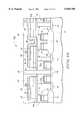
- a semiconductor wafer fragment in processis indicated generally with reference numeral 10.
- Suchcomprises a bulk semiconductor silicon substrate 12 having an electrically conductive diffusion region 14 provided therein. Region 14 constitutes a node to which electrical connection to a capacitor is to be made.
- An insulating layer 16typically borophosphosilicate glass (BPSG), overlies substrate 12 and includes a previously provided contact opening 18 over node 14.
- Contact opening 18is filled with an electrically conductive first material 20 which electrically connects with node 14.
- component 20comprises a material which is reactive to form an electrically insulative material (i.e., insulative oxides or insulative nitrides).
- An example and preferred materialis conductively doped polysilicon which readily oxidizes to insulating SiO 2 .
- An etch stop layer 21is provided atop insulating layer 16, with the composite structure being provided with an upper planarized surface as shown.
- an electrically insulative barrier second layer 22is provided over first conductive layer 20.
- An example and preferred thickness for layer 22is 1000 Angstroms.
- Example and preferred materials for layer 22include Al 2 O 3 , TiO 2 , Si 3 N 4 , SiO 2 and AlN, or mixtures thereof.
- Such layerwill provide at least one or two barrier functions.
- barrier second layer 22will be designed to serve the function of restricting such reaction at a later step in the process, as will be apparent subsequently.
- layer 22serves the function of preventing out-diffusion of layer 20 components.
- a third layer 24is provided over electrically insulative barrier layer 22.
- An example and preferred thicknessis 1000 Angstroms.
- Third layer 24comprises a material which is either electrically conductive and resistant to oxidation (i.e., elemental platinum), or a material which forms an electrically conductive material upon oxidation (i.e., elemental Ru which upon oxidation is transformed to a conductive RuO 2 ).
- Layers 20, 22, and 24comprise components of a capacitor plate.
- an insulating inorganic metal oxide dielectric layer 26is provided over electrically conductive third layer 24.
- Example insulating inorganic metal oxide materials usable in accordance with the inventioninclude ferroelectrics or other perovskite materials, or other materials, such as titanates, zirconates, niobates, tantalates and nitrates, such as those shown below.
- Deposition of such materialstypically involves chemical vapor deposition involving oxygen which would lead to oxidation of electrically conductive first layer 20 were oxidation barrier layer 22 not present. Further even after deposition of such materials, densification of such layers typically occurs to complete the provision of the desired material. Such typically occurs in an oxygen rich atmosphere at elevated temperatures, which also would oxidize the preferred polysilicon material of layer 20 were layer 22 not present. Accordingly in such instance, barrier second layer 22 restricts oxidation of first electrically conductive layer 20 during provision of insulating inorganic metal oxide dielectric layer 26. Barrier layer 22 also prevents interaction of layer 24 with layer 20.
- An electrically conductive fourth layer 28is provided over insulating inorganic metal oxide dielectric layer 26, with 1000 Angstroms being an example preferred thickness.
- a preferred material for layer 28is Pt, Ru or RuO x .
- layers 28, 26 and 24are patterned and etched selectively relative to barrier layer 22 to effectively define the outline of a desired capacitor shape.
- Layer 28effectively comprises a second capacitor plate, while layers 24, 22 and 20 comprise first capacitor plate components.
- polysilicon layer 20is electrically isolated from layer 24 by insulating barrier layer 22.
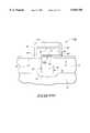
- a layer of SiO 2is deposited and anisotropically etched to produce oxide spacers 30.
- Such spacersprotect dielectric layer 26 from a conductive layer deposition described below.
- an isotropic undercut etching of oxidation barrier layer 22is conducted selectively relative to polysilicon, nitride and the material of layer 24 to expose first and third layers 20 and 24, respectively.
- An example etch chemistrywould be hot sulfuric acid to etch a TiO 2 layer, or ammonium hydroxide to etch an Al 2 O 3 layer.
- first layer 20comprises outermost peripheral sidewalls 32
- oxidation barrier second layer 22comprises outermost peripheral sidewalls 34
- third layer 24comprises outermost peripheral sidewalls 36.
- second layer sidewalls 34are received entirely within the peripheral confines of both the first and third layer sidewalls 32 and 36, respectively.
- a highly conformal electrically conductive layer 38is chemical vapor deposited over the wafer to fill the void beneath layer 24 and spacers 30.
- electrically conductive layer 38is conformally deposited over exposed first layer 20 and exposed third layer 24.
- Example and preferred materialsare TiN and W.
- Wcan be chemical vapor deposited using WF 6 and H 2 as precursors at 450° C. and 80 Torr.
- TiNcan be deposited using either TiCl 4 and NH 3 , or tetrakisdimethylamido titanium, as precursors.
- Layer 38is then etched (wet etch using a 1:1 mix of NH 4 OH and H 2 O 2 for either TiN or W) to produce a surrounding electrically conductive interconnect 40 which extends around second insulative oxidation barrier layer 22 and electrically interconnects first conductive layer 20 and third conductive layer 24. Accordingly, electrically interconnecting link 40 is at least partially received within the peripheral confines of first sidewalls 32 and third sidewalls 36 (FIG. 6). In the described and preferred sequence, the final patterning to produce interconnect 40 occurs last in the above stated steps.
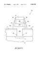
- FIGS. 9-19One example alternate and integrated sequence of processing steps are shown and described with reference to FIGS. 9-19 in fabrication of a bit line over stacked capacitor DRAM construction. Like numerals is are utilized from the previous embodiment where appropriate, with differences being indicated with the suffix "a" or different numerals.
- wafer fragment 10acomprises bulk substrate 12 having diffusion regions 14, 15, 17, 19, and field oxide regions 42 provided therein.
- a series of word lines 43, 44, 45, 46, 47 and 48are provided.
- An insulating layer 16ais also provided, and has contacts 18, 61 and 63 provided therethrough. Such are filled by a first conductive polysilicon layer 20a.
- oxidation barrier layer 22 and third conductive layer 24are provided.
- layers 24, 22, and 20aare patterned as shown to provide the indicated outlines of first capacitor plates 25, 27 and 29.
- insulating inorganic metal oxide dielectric layer 26 and third conductive layer 28are provided.
- layer 22comprises SiO 2 , which provides an inherent diffusion barrier function but not an inherent antioxidation function
- layer 22might grow to the FIG. 12 illustrated size 22a. In such instance, the thickness of original layer 22, more so than its composition, provides the predominant barrier function to undesired reaction of layer 20a.
- layers 26 and 28are patterned and etched over what will be a bit contact node 15.
- oxidation barrier layer 22is undercut etched selectively relative to first conductive layer 20 and conductive third layer 24 to outwardly expose such layers.
- a conformal layer 38a of TiN or another conductive materialis chemical vapor deposited atop the substrate to completely fill the voids created by the undercut etching.
- layer 38ais wet or dry etched to produce the illustrated electrically conductive interconnects 40a which extend around second insulative layer 22 and electrically interconnect the first layer 20 and the third layer 24 of the respective capacitors. Note that in accordance with this described embodiment, electrical interconnecting link 40a is received entirely within the peripheral confines of the outer sidewalls of layers 20a and 24.
- an insulative layer 50is deposited to protect the edge of dielectric layer 26.
- a layer 52 of borophosphosilicate glassis deposited and planarized.
- a contact opening 54is provided therein and etched to outwardly expose bit node 15. Subsequently, contact 54 is filled with a conductive plug filling material 56, such as tungsten. Thereafter, a conductive layer would be provided atop plug 56 and BPSG layer 52 and patterned into desired bit lines.
- a conductive plug filling material 56such as tungsten.
- the above described methodprovides the advantage of utilizing good barrier layers which are electrically insulative, as opposed to the prior art's essential use of conductive barrier layers which limits choices.
- FIG. 20Another alternate embodiment is shown in FIG. 20. Like numerals are utilized from the first described embodiment where appropriate, with differences being indicated with the suffix "b" or different numerals.
- FIG. 20 embodiment 10bis analogous to that shown in FIG. 8. The difference is that barrier second layer 22b comprises discrete electrically insulative layers 23 and 31 of different materials. This design might be desired where both reaction and diffusion barrier properties are desired for layer 22, and using separate layers for the separate functions.
- FIG. 21Yet another alternate embodiment is shown in FIG. 21. Like numerals are utilized from the first described embodiment where appropriate, with differences being indicated with the suffix "c" or different numerals.
- Construction 10cplaces a portion of first layer 20c above layer 21 such that outer sidewalls thereof can be exposed outwardly of layer 21. Accordingly, undercut etching of layer 22 is not conducted for the purpose of exposing layers 20c and 24c for electrical interconnect.
- An insulating cap 78 and spacers 80are provided as shown relative to the upper capacitor plate 28c and dielectric layer 26c. Thereafter, an electrically conductive layer, such as TiN, is deposited and anisotropically etched to produce conductive interconnecting links 40c with join layers 24c and 20c.
Landscapes
- Engineering & Computer Science (AREA)
- Manufacturing & Machinery (AREA)
- Semiconductor Integrated Circuits (AREA)
- Semiconductor Memories (AREA)
Abstract
Description
______________________________________Barium Titanate BaTiO.sub.3Barium Strontium Titanate (Ba,Sr)TiO.sub.3Barium Lead Titanate (Ba,Pb)TiO.sub.3Lead Titanate PbTiO.sub.3Lead Zirconate PbZnO.sub.3Lead Zirconate Titanate Pb(Zn,Ti)O.sub.3Lead Lanthinum Titanate (Pb,La)TiO.sub.3Lead Lanthinum Zirconate (Pb,La)(Zn,Ti)O.sub.3TitanateStrontium Titanate SrTiO.sub.3Potassium Nitrate KNO.sub.3Lithium Niobate LiNbO.sub.3Lithium Tantalate LiTaO.sub.3Lead Magnesium Niobate Pb(Mg,Nb)O.sub.3(Mixed phases) Pb(Mg,Nb)O.sub.3 :PbTiO.sub.3Bismuth Titanate Bi.sub.4 Ti.sub.3 O.sub.12______________________________________
Claims (41)
Priority Applications (1)
| Application Number | Priority Date | Filing Date | Title |
|---|---|---|---|
| US08/738,789US5955758A (en) | 1995-05-17 | 1996-10-29 | Method of forming a capacitor plate and a capacitor incorporating same |
Applications Claiming Priority (2)
| Application Number | Priority Date | Filing Date | Title |
|---|---|---|---|
| US08/442,837US5654222A (en) | 1995-05-17 | 1995-05-17 | Method for forming a capacitor with electrically interconnected construction |
| US08/738,789US5955758A (en) | 1995-05-17 | 1996-10-29 | Method of forming a capacitor plate and a capacitor incorporating same |
Related Parent Applications (1)
| Application Number | Title | Priority Date | Filing Date |
|---|---|---|---|
| US08/442,837DivisionUS5654222A (en) | 1995-05-17 | 1995-05-17 | Method for forming a capacitor with electrically interconnected construction |
Publications (1)
| Publication Number | Publication Date |
|---|---|
| US5955758Atrue US5955758A (en) | 1999-09-21 |
Family
ID=23758352
Family Applications (3)
| Application Number | Title | Priority Date | Filing Date |
|---|---|---|---|
| US08/442,837Expired - LifetimeUS5654222A (en) | 1995-05-17 | 1995-05-17 | Method for forming a capacitor with electrically interconnected construction |
| US08/738,789Expired - LifetimeUS5955758A (en) | 1995-05-17 | 1996-10-29 | Method of forming a capacitor plate and a capacitor incorporating same |
| US08/858,027Expired - LifetimeUS5985714A (en) | 1995-05-17 | 1997-05-16 | Method of forming a capacitor |
Family Applications Before (1)
| Application Number | Title | Priority Date | Filing Date |
|---|---|---|---|
| US08/442,837Expired - LifetimeUS5654222A (en) | 1995-05-17 | 1995-05-17 | Method for forming a capacitor with electrically interconnected construction |
Family Applications After (1)
| Application Number | Title | Priority Date | Filing Date |
|---|---|---|---|
| US08/858,027Expired - LifetimeUS5985714A (en) | 1995-05-17 | 1997-05-16 | Method of forming a capacitor |
Country Status (1)
| Country | Link |
|---|---|
| US (3) | US5654222A (en) |
Cited By (47)
| Publication number | Priority date | Publication date | Assignee | Title |
|---|---|---|---|---|
| US6165839A (en)* | 1998-06-08 | 2000-12-26 | Taiwan Semiconductor Manufacturing Company | Process to fabricate a cylindrical, capacitor structure under a bit line structure for a dynamic random access memory cell |
| US6165834A (en)* | 1998-05-07 | 2000-12-26 | Micron Technology, Inc. | Method of forming capacitors, method of processing dielectric layers, method of forming a DRAM cell |
| US6200850B1 (en)* | 1999-11-30 | 2001-03-13 | United Microelectronics Corp. | Method for forming a stacked capacitor |
| US6285050B1 (en)* | 1997-12-24 | 2001-09-04 | International Business Machines Corporation | Decoupling capacitor structure distributed above an integrated circuit and method for making same |
| US6300654B1 (en)* | 1999-04-30 | 2001-10-09 | Stmicroelectronics S.R.L. | Structure of a stacked memory cell, in particular a ferroelectric cell |
| US6351005B1 (en)* | 1998-09-17 | 2002-02-26 | Micron Technology, Inc. | Integrated capacitor incorporating high K dielectric |
| US6400552B2 (en) | 1998-02-28 | 2002-06-04 | Micron Technology, Inc. | Capacitor with conductively doped Si-Ge alloy electrode |
| US6407452B1 (en) | 1998-04-10 | 2002-06-18 | Micron Technology, Inc. | Integrated circuitry and method of restricting diffusion from one material to another |
| US6429473B1 (en)* | 1996-07-30 | 2002-08-06 | International Business Machines Corporation | DRAM cell with stacked capacitor self-aligned to bitline |
| US6452272B1 (en)* | 1999-06-29 | 2002-09-17 | Koninklijke Philips Electronics N.V. | Semiconductor device |
| US6476432B1 (en) | 2000-03-23 | 2002-11-05 | Micron Technology, Inc. | Structures and methods for enhancing capacitors in integrated circuits |
| US6607975B1 (en) | 1998-11-25 | 2003-08-19 | Micron Technology, Inc. | Device and method for protecting against oxidation of a conductive layer in said device |
| US6627508B1 (en) | 1997-08-20 | 2003-09-30 | Micron Technology, Inc. | Method of forming capacitors containing tantalum |
| US20030211673A1 (en)* | 1997-12-18 | 2003-11-13 | Yoshitaka Nakamura | Dynamic random access memory with improved contact arrangements |
| US6667502B1 (en) | 1999-08-31 | 2003-12-23 | Micron Technology, Inc. | Structurally-stabilized capacitors and method of making of same |
| US20040058493A1 (en)* | 1999-04-30 | 2004-03-25 | Stmicroelectronics S.R.I. | Method of fabricating a ferroelectric stacked memory cell |
| US6753564B2 (en)* | 1998-09-10 | 2004-06-22 | Hyundai Microelectronics Co., Ltd. | Capacitor of semiconductor device and method of fabricating the same |
| US20040175898A1 (en)* | 1998-11-25 | 2004-09-09 | Agarwal Vishnu K. | Device and method for protecting against oxidation of a conductive layer in said device |
| US20050051822A1 (en)* | 2003-09-04 | 2005-03-10 | Manning Homer M. | Support for vertically oriented capacitors during the formation of a semiconductor device |
| US20050054159A1 (en)* | 2003-09-04 | 2005-03-10 | Manning H. Montgomery | Semiconductor constructions, and methods of forming capacitor devices |
| US6891217B1 (en) | 1998-04-10 | 2005-05-10 | Micron Technology, Inc. | Capacitor with discrete dielectric material |
| US6953721B2 (en) | 2000-02-23 | 2005-10-11 | Micron Technology, Inc. | Methods of forming a capacitor with an amorphous and a crystalline high K capacitor dielectric region |
| EP1584102A1 (en)* | 2003-01-07 | 2005-10-12 | Infineon Technologies AG | Encapsulation of ferroelectric capacitors |
| US20060014344A1 (en)* | 2004-07-19 | 2006-01-19 | Manning H M | Methods of forming semiconductor structures and capacitor devices |
| US20060011959A1 (en)* | 2004-07-19 | 2006-01-19 | Jae-Hyun Park | Semiconductor devices having a planarized insulating layer and methods of forming the same |
| US20060051918A1 (en)* | 2004-08-27 | 2006-03-09 | Busch Brett W | Methods of forming a plurality of capacitors |
| US7053433B1 (en)* | 2002-04-29 | 2006-05-30 | Celis Semiconductor Corp. | Encapsulated ferroelectric array |
| US20060121672A1 (en)* | 2004-12-06 | 2006-06-08 | Cem Basceri | Methods of forming pluralities of capacitors, and integrated circuitry |
| US20060148190A1 (en)* | 2004-08-30 | 2006-07-06 | Busch Brett W | Methods of forming a plurality of capacitors |
| US20060211211A1 (en)* | 2005-03-18 | 2006-09-21 | Sandhu Gurtej S | Methods of forming pluralities of capacitors |
| US20060256597A1 (en)* | 2005-05-13 | 2006-11-16 | Stmicroelectronics S.R.L | Method and relative circuit for generating a control voltage of a synchronous rectifier |
| US20060263968A1 (en)* | 2005-05-18 | 2006-11-23 | Micron Technology, Inc. | Methods of forming pluralities of capacitors |
| US20070032014A1 (en)* | 2005-08-02 | 2007-02-08 | Micron Technology, Inc. | Methods of forming pluralities of capacitors |
| US20070161202A1 (en)* | 2004-08-27 | 2007-07-12 | Manning H M | Methods of forming a plurality of capacitors |
| US20070196978A1 (en)* | 2005-05-18 | 2007-08-23 | Manning H M | Integrated circuitry comprising a pair of adjacent capacitors |
| US20070238259A1 (en)* | 2006-04-10 | 2007-10-11 | Micron Technology, Inc. | Methods of forming a plurality of capacitors |
| US20090251845A1 (en)* | 2008-04-08 | 2009-10-08 | Micron Technology, Inc. | High aspect ratio openings |
| US7682924B2 (en) | 2007-08-13 | 2010-03-23 | Micron Technology, Inc. | Methods of forming a plurality of capacitors |
| US7759193B2 (en) | 2008-07-09 | 2010-07-20 | Micron Technology, Inc. | Methods of forming a plurality of capacitors |
| US7785962B2 (en) | 2007-02-26 | 2010-08-31 | Micron Technology, Inc. | Methods of forming a plurality of capacitors |
| US7902081B2 (en) | 2006-10-11 | 2011-03-08 | Micron Technology, Inc. | Methods of etching polysilicon and methods of forming pluralities of capacitors |
| US8388851B2 (en) | 2008-01-08 | 2013-03-05 | Micron Technology, Inc. | Capacitor forming methods |
| US8518788B2 (en) | 2010-08-11 | 2013-08-27 | Micron Technology, Inc. | Methods of forming a plurality of capacitors |
| US8652926B1 (en) | 2012-07-26 | 2014-02-18 | Micron Technology, Inc. | Methods of forming capacitors |
| US8946043B2 (en) | 2011-12-21 | 2015-02-03 | Micron Technology, Inc. | Methods of forming capacitors |
| US9076680B2 (en) | 2011-10-18 | 2015-07-07 | Micron Technology, Inc. | Integrated circuitry, methods of forming capacitors, and methods of forming integrated circuitry comprising an array of capacitors and circuitry peripheral to the array |
| US10515801B2 (en) | 2007-06-04 | 2019-12-24 | Micron Technology, Inc. | Pitch multiplication using self-assembling materials |
Families Citing this family (42)
| Publication number | Priority date | Publication date | Assignee | Title |
|---|---|---|---|---|
| US5773363A (en)* | 1994-11-08 | 1998-06-30 | Micron Technology, Inc. | Semiconductor processing method of making electrical contact to a node |
| US6699530B2 (en)* | 1995-07-06 | 2004-03-02 | Applied Materials, Inc. | Method for constructing a film on a semiconductor wafer |
| US5654222A (en)* | 1995-05-17 | 1997-08-05 | Micron Technology, Inc. | Method for forming a capacitor with electrically interconnected construction |
| US5786248A (en)* | 1995-10-12 | 1998-07-28 | Micron Technology, Inc. | Semiconductor processing method of forming a tantalum oxide containing capacitor |
| KR100189982B1 (en)* | 1995-11-29 | 1999-06-01 | 윤종용 | Manufacturing method of high dielectric capacitor |
| US5843830A (en) | 1996-06-26 | 1998-12-01 | Micron Technology, Inc. | Capacitor, and methods for forming a capacitor |
| DE19630110C2 (en)* | 1996-07-25 | 1998-11-19 | Siemens Ag | Layer structure with a ferroelectric layer and manufacturing process |
| US6251720B1 (en) | 1996-09-27 | 2001-06-26 | Randhir P. S. Thakur | High pressure reoxidation/anneal of high dielectric constant materials |
| JP3090198B2 (en)* | 1997-08-21 | 2000-09-18 | 日本電気株式会社 | Structure of semiconductor device and method of manufacturing the same |
| US6200874B1 (en) | 1997-08-22 | 2001-03-13 | Micron Technology, Inc. | Methods for use in forming a capacitor |
| US6911371B2 (en) | 1997-12-19 | 2005-06-28 | Micron Technology, Inc. | Capacitor forming methods with barrier layers to threshold voltage shift inducing material |
| US6165833A (en) | 1997-12-19 | 2000-12-26 | Micron Technology, Inc. | Semiconductor processing method of forming a capacitor |
| US6162744A (en)* | 1998-02-28 | 2000-12-19 | Micron Technology, Inc. | Method of forming capacitors having high-K oxygen containing capacitor dielectric layers, method of processing high-K oxygen containing dielectric layers, method of forming a DRAM cell having having high-K oxygen containing capacitor dielectric layers |
| US6255186B1 (en) | 1998-05-21 | 2001-07-03 | Micron Technology, Inc. | Methods of forming integrated circuitry and capacitors having a capacitor electrode having a base and a pair of walls projecting upwardly therefrom |
| KR20000001945A (en)* | 1998-06-15 | 2000-01-15 | 윤종용 | D-ram cell capacitor manufacturing method |
| KR100290895B1 (en)* | 1998-06-30 | 2001-07-12 | 김영환 | Capacitor structure of semiconductor device and manufacturing method thereof |
| US6271131B1 (en) | 1998-08-26 | 2001-08-07 | Micron Technology, Inc. | Methods for forming rhodium-containing layers such as platinum-rhodium barrier layers |
| US6239028B1 (en)* | 1998-09-03 | 2001-05-29 | Micron Technology, Inc. | Methods for forming iridium-containing films on substrates |
| US6323081B1 (en) | 1998-09-03 | 2001-11-27 | Micron Technology, Inc. | Diffusion barrier layers and methods of forming same |
| US6284655B1 (en) | 1998-09-03 | 2001-09-04 | Micron Technology, Inc. | Method for producing low carbon/oxygen conductive layers |
| US6780758B1 (en) | 1998-09-03 | 2004-08-24 | Micron Technology, Inc. | Method of establishing electrical contact between a semiconductor substrate and a semiconductor device |
| KR100286342B1 (en)* | 1998-09-18 | 2001-04-16 | 김영환 | Manufacturing method for capacitor |
| US6387748B1 (en) | 1999-02-16 | 2002-05-14 | Micron Technology, Inc. | Semiconductor circuit constructions, capacitor constructions, and methods of forming semiconductor circuit constructions and capacitor constructions |
| US6600185B1 (en)* | 1999-03-10 | 2003-07-29 | Oki Electric Industry Co., Ltd. | Ferroelectric capacitor with dielectric lining, semiconductor memory device employing same, and fabrication methods thereof |
| US6445023B1 (en)* | 1999-03-16 | 2002-09-03 | Micron Technology, Inc. | Mixed metal nitride and boride barrier layers |
| US6329286B1 (en) | 1999-04-27 | 2001-12-11 | Micron Technology, Inc. | Methods for forming conformal iridium layers on substrates |
| KR100312384B1 (en)* | 1999-06-30 | 2001-11-03 | 박종섭 | Method of forming a capacitor in a semiconductor |
| KR100390938B1 (en)* | 2000-02-09 | 2003-07-10 | 주식회사 하이닉스반도체 | Method of manufacturing a capacitor in a semiconductor device |
| US6617206B1 (en)* | 2000-06-07 | 2003-09-09 | Micron Technology, Inc. | Method of forming a capacitor structure |
| US6429127B1 (en)* | 2000-06-08 | 2002-08-06 | Micron Technology, Inc. | Methods for forming rough ruthenium-containing layers and structures/methods using same |
| US6482736B1 (en) | 2000-06-08 | 2002-11-19 | Micron Technology, Inc. | Methods for forming and integrated circuit structures containing enhanced-surface-area conductive layers |
| US7253076B1 (en)* | 2000-06-08 | 2007-08-07 | Micron Technologies, Inc. | Methods for forming and integrated circuit structures containing ruthenium and tungsten containing layers |
| US6451646B1 (en)* | 2000-08-30 | 2002-09-17 | Micron Technology, Inc. | High-k dielectric materials and processes for manufacturing them |
| US6555487B1 (en) | 2000-08-31 | 2003-04-29 | Micron Technology, Inc. | Method of selective oxidation conditions for dielectric conditioning |
| US6660631B1 (en)* | 2000-08-31 | 2003-12-09 | Micron Technology, Inc. | Devices containing platinum-iridium films and methods of preparing such films and devices |
| US6518198B1 (en) | 2000-08-31 | 2003-02-11 | Micron Technology, Inc. | Electroless deposition of doped noble metals and noble metal alloys |
| US7378719B2 (en)* | 2000-12-20 | 2008-05-27 | Micron Technology, Inc. | Low leakage MIM capacitor |
| JP3921401B2 (en)* | 2002-03-15 | 2007-05-30 | 松下電器産業株式会社 | Capacitor element manufacturing method |
| US6916722B2 (en)* | 2002-12-02 | 2005-07-12 | Taiwan Semiconductor Manufacturing Co., Ltd. | Method to fabricate high reliable metal capacitor within copper back-end process |
| US8008162B2 (en)* | 2008-11-19 | 2011-08-30 | Micron Technology, Inc. | Select devices including an open volume, memory devices and systems including same, and methods for forming same |
| US8378453B2 (en)* | 2011-04-29 | 2013-02-19 | Georgia Tech Research Corporation | Devices including composite thermal capacitors |
| US9777372B2 (en)* | 2013-08-07 | 2017-10-03 | Regents Of The University Of Minnesota | Methods for manufacturing nano-gap and angstrom-gap articles |
Citations (5)
| Publication number | Priority date | Publication date | Assignee | Title |
|---|---|---|---|---|
| US5371700A (en)* | 1992-10-19 | 1994-12-06 | Sharp Kabushiki Kaisha | Semiconductor memory device with covered sidewall spacers |
| US5418388A (en)* | 1993-06-18 | 1995-05-23 | Mitsubishi Denki Kabushiki Kaisha | Semiconductor device having a capacitor with an adhesion layer |
| US5449934A (en)* | 1992-02-18 | 1995-09-12 | Matsushita Electric Industrial Co., Ltd. | Semiconductor memory device and process |
| US5486713A (en)* | 1993-01-05 | 1996-01-23 | Nec Corporation | Semiconductor device having a capacitor |
| US5561307A (en)* | 1992-07-23 | 1996-10-01 | Symetrix Corporation | Ferroelectric integrated circuit |
Family Cites Families (3)
| Publication number | Priority date | Publication date | Assignee | Title |
|---|---|---|---|---|
| JP2886280B2 (en)* | 1990-06-29 | 1999-04-26 | 宮城沖電気株式会社 | Method for manufacturing semiconductor memory device |
| US5053351A (en)* | 1991-03-19 | 1991-10-01 | Micron Technology, Inc. | Method of making stacked E-cell capacitor DRAM cell |
| US5654222A (en)* | 1995-05-17 | 1997-08-05 | Micron Technology, Inc. | Method for forming a capacitor with electrically interconnected construction |
- 1995
- 1995-05-17USUS08/442,837patent/US5654222A/ennot_activeExpired - Lifetime
- 1996
- 1996-10-29USUS08/738,789patent/US5955758A/ennot_activeExpired - Lifetime
- 1997
- 1997-05-16USUS08/858,027patent/US5985714A/ennot_activeExpired - Lifetime
Patent Citations (5)
| Publication number | Priority date | Publication date | Assignee | Title |
|---|---|---|---|---|
| US5449934A (en)* | 1992-02-18 | 1995-09-12 | Matsushita Electric Industrial Co., Ltd. | Semiconductor memory device and process |
| US5561307A (en)* | 1992-07-23 | 1996-10-01 | Symetrix Corporation | Ferroelectric integrated circuit |
| US5371700A (en)* | 1992-10-19 | 1994-12-06 | Sharp Kabushiki Kaisha | Semiconductor memory device with covered sidewall spacers |
| US5486713A (en)* | 1993-01-05 | 1996-01-23 | Nec Corporation | Semiconductor device having a capacitor |
| US5418388A (en)* | 1993-06-18 | 1995-05-23 | Mitsubishi Denki Kabushiki Kaisha | Semiconductor device having a capacitor with an adhesion layer |
Non-Patent Citations (6)
| Title |
|---|
| Eimori, T. et al., "A Newly Designed Planar Stacked Capacitor Cell With High Dielectric Constant Film for 256Mbit DRAM", IEEE, 1993, pp. 631-634. |
| Eimori, T. et al., A Newly Designed Planar Stacked Capacitor Cell With High Dielectric Constant Film for 256Mbit DRAM , IEEE, 1993, pp. 631 634.* |
| Lesaicherre, P Y et al., A Gbit Scale DRAM Stacked Capacitor Technology With ECR MOCVD SrTiO 3 and RIE Patterned RuO 2 /TiN Storage Node , IEEE, 1994, pp. 831 834.* |
| Lesaicherre, P-Y et al., "A Gbit-Scale DRAM Stacked Capacitor Technology With ECR MOCVD SrTiO3 and RIE Patterned RuO2 /TiN Storage Node", IEEE, 1994, pp. 831-834. |
| Onishi, Shigeo et al., "A Half-Micron Ferroelectric Memory Cell Technology with Stacked Capacitor Structure", IEEE, 1994, pp. 843-846. |
| Onishi, Shigeo et al., A Half Micron Ferroelectric Memory Cell Technology with Stacked Capacitor Structure , IEEE, 1994, pp. 843 846.* |
Cited By (123)
| Publication number | Priority date | Publication date | Assignee | Title |
|---|---|---|---|---|
| US6429473B1 (en)* | 1996-07-30 | 2002-08-06 | International Business Machines Corporation | DRAM cell with stacked capacitor self-aligned to bitline |
| US6627508B1 (en) | 1997-08-20 | 2003-09-30 | Micron Technology, Inc. | Method of forming capacitors containing tantalum |
| US20030211673A1 (en)* | 1997-12-18 | 2003-11-13 | Yoshitaka Nakamura | Dynamic random access memory with improved contact arrangements |
| US6285050B1 (en)* | 1997-12-24 | 2001-09-04 | International Business Machines Corporation | Decoupling capacitor structure distributed above an integrated circuit and method for making same |
| US6400552B2 (en) | 1998-02-28 | 2002-06-04 | Micron Technology, Inc. | Capacitor with conductively doped Si-Ge alloy electrode |
| US6773981B1 (en) | 1998-02-28 | 2004-08-10 | Micron Technology, Inc. | Methods of forming capacitors |
| US7166885B2 (en) | 1998-04-10 | 2007-01-23 | Micron Technology, Inc. | Semiconductor devices |
| US6891217B1 (en) | 1998-04-10 | 2005-05-10 | Micron Technology, Inc. | Capacitor with discrete dielectric material |
| US6407452B1 (en) | 1998-04-10 | 2002-06-18 | Micron Technology, Inc. | Integrated circuitry and method of restricting diffusion from one material to another |
| US6995419B2 (en) | 1998-04-10 | 2006-02-07 | Micron Technology, Inc. | Semiconductor constructions having crystalline dielectric layers |
| US6165834A (en)* | 1998-05-07 | 2000-12-26 | Micron Technology, Inc. | Method of forming capacitors, method of processing dielectric layers, method of forming a DRAM cell |
| US6165839A (en)* | 1998-06-08 | 2000-12-26 | Taiwan Semiconductor Manufacturing Company | Process to fabricate a cylindrical, capacitor structure under a bit line structure for a dynamic random access memory cell |
| US6753564B2 (en)* | 1998-09-10 | 2004-06-22 | Hyundai Microelectronics Co., Ltd. | Capacitor of semiconductor device and method of fabricating the same |
| US6351005B1 (en)* | 1998-09-17 | 2002-02-26 | Micron Technology, Inc. | Integrated capacitor incorporating high K dielectric |
| US6720215B1 (en) | 1998-11-25 | 2004-04-13 | Micron Technology, Inc. | Device and method for protecting against oxidation of a conductive layer in said device |
| US7041550B1 (en) | 1998-11-25 | 2006-05-09 | Micron Technology, Inc. | Device and method for protecting against oxidation of a conductive layer in said device |
| US7067861B1 (en) | 1998-11-25 | 2006-06-27 | Micron Technology, Inc. | Device and method for protecting against oxidation of a conductive layer in said device |
| US6972452B2 (en) | 1998-11-25 | 2005-12-06 | Micron Technology, Inc. | Device and method for protecting against oxidation of a conductive layer in said device |
| US6607975B1 (en) | 1998-11-25 | 2003-08-19 | Micron Technology, Inc. | Device and method for protecting against oxidation of a conductive layer in said device |
| US7049191B1 (en) | 1998-11-25 | 2006-05-23 | Micron Technology, Inc. | Method for protecting against oxidation of a conductive layer in said device |
| US7094657B1 (en) | 1998-11-25 | 2006-08-22 | Micron Technology, Inc. | Method for protecting against oxidation of a conductive layer in said device |
| US20040175898A1 (en)* | 1998-11-25 | 2004-09-09 | Agarwal Vishnu K. | Device and method for protecting against oxidation of a conductive layer in said device |
| US6808976B1 (en) | 1998-11-25 | 2004-10-26 | Micron Technology, Inc. | Device and method for protecting against oxidation of a conductive layer in said device |
| US6852622B1 (en) | 1998-11-25 | 2005-02-08 | Micron Technology, Inc. | Device and method for protecting against oxidation of a conductive layer in said device |
| US6924188B1 (en) | 1998-11-25 | 2005-08-02 | Micron Technology, Inc. | Device and method for protecting against oxidation of a conductive layer in said device |
| US6916699B1 (en) | 1998-11-25 | 2005-07-12 | Micron Technology, Inc. | Device and method for protecting against oxidation of a conductive layer in said device |
| US6897512B2 (en)* | 1998-11-25 | 2005-05-24 | Micron Technology, Inc. | Device and method for protecting against oxidation of a conductive layer in said device |
| US6656801B2 (en) | 1999-04-30 | 2003-12-02 | Stmicroelectronics S.R.L. | Method of fabricating a ferroelectric stacked memory cell |
| US20040058493A1 (en)* | 1999-04-30 | 2004-03-25 | Stmicroelectronics S.R.I. | Method of fabricating a ferroelectric stacked memory cell |
| US6300654B1 (en)* | 1999-04-30 | 2001-10-09 | Stmicroelectronics S.R.L. | Structure of a stacked memory cell, in particular a ferroelectric cell |
| US6872996B2 (en) | 1999-04-30 | 2005-03-29 | Stmicroelectronics S.R.L. | Method of fabricating a ferroelectric stacked memory cell |
| US6452272B1 (en)* | 1999-06-29 | 2002-09-17 | Koninklijke Philips Electronics N.V. | Semiconductor device |
| US7488665B2 (en) | 1999-08-31 | 2009-02-10 | Micron Technology, Inc. | Structurally-stabilized capacitors and method of making of same |
| US6667502B1 (en) | 1999-08-31 | 2003-12-23 | Micron Technology, Inc. | Structurally-stabilized capacitors and method of making of same |
| US7282756B2 (en) | 1999-08-31 | 2007-10-16 | Micron Technology Inc. | Structurally-stabilized capacitors and method of making of same |
| US6200850B1 (en)* | 1999-11-30 | 2001-03-13 | United Microelectronics Corp. | Method for forming a stacked capacitor |
| US7446363B2 (en) | 2000-02-23 | 2008-11-04 | Micron Technology, Inc. | Capacitor including a percentage of amorphous dielectric material and a percentage of crystalline dielectric material |
| US6953721B2 (en) | 2000-02-23 | 2005-10-11 | Micron Technology, Inc. | Methods of forming a capacitor with an amorphous and a crystalline high K capacitor dielectric region |
| US7005695B1 (en) | 2000-02-23 | 2006-02-28 | Micron Technology, Inc. | Integrated circuitry including a capacitor with an amorphous and a crystalline high K capacitor dielectric region |
| US6696716B2 (en) | 2000-03-23 | 2004-02-24 | Micron Technology, Inc. | Structures and methods for enhancing capacitors in integrated ciruits |
| US6861330B2 (en) | 2000-03-23 | 2005-03-01 | Micron Technology Inc. | Structures and methods for enhancing capacitors in integrated circuits |
| US6476432B1 (en) | 2000-03-23 | 2002-11-05 | Micron Technology, Inc. | Structures and methods for enhancing capacitors in integrated circuits |
| US7053433B1 (en)* | 2002-04-29 | 2006-05-30 | Celis Semiconductor Corp. | Encapsulated ferroelectric array |
| EP1584102A1 (en)* | 2003-01-07 | 2005-10-12 | Infineon Technologies AG | Encapsulation of ferroelectric capacitors |
| US7067385B2 (en) | 2003-09-04 | 2006-06-27 | Micron Technology, Inc. | Support for vertically oriented capacitors during the formation of a semiconductor device |
| US20050054159A1 (en)* | 2003-09-04 | 2005-03-10 | Manning H. Montgomery | Semiconductor constructions, and methods of forming capacitor devices |
| US8786001B2 (en) | 2003-09-04 | 2014-07-22 | Round Rock Research, Llc | Semiconductor devices |
| US20060063345A1 (en)* | 2003-09-04 | 2006-03-23 | Manning H M | Methods of forming plurality of capacitor devices |
| US20100117196A1 (en)* | 2003-09-04 | 2010-05-13 | Manning Homer M | Support For Vertically-Oriented Capacitors During The Formation of a Semiconductor Device |
| US20050051822A1 (en)* | 2003-09-04 | 2005-03-10 | Manning Homer M. | Support for vertically oriented capacitors during the formation of a semiconductor device |
| US20060063344A1 (en)* | 2003-09-04 | 2006-03-23 | Manning H M | Methods of forming a plurality of capacitor devices |
| US20050287780A1 (en)* | 2003-09-04 | 2005-12-29 | Micron Technology, Inc. | Semiconductor constructions |
| US7449391B2 (en) | 2003-09-04 | 2008-11-11 | Micron Technology, Inc. | Methods of forming plurality of capacitor devices |
| US7125781B2 (en) | 2003-09-04 | 2006-10-24 | Micron Technology, Inc. | Methods of forming capacitor devices |
| US7271051B2 (en) | 2003-09-04 | 2007-09-18 | Micron Technology, Inc. | Methods of forming a plurality of capacitor devices |
| US7420238B2 (en) | 2003-09-04 | 2008-09-02 | Micron Technology, Inc. | Semiconductor constructions |
| US20050158949A1 (en)* | 2003-09-04 | 2005-07-21 | Manning Homer M. | Semiconductor devices |
| US7655968B2 (en) | 2003-09-04 | 2010-02-02 | Micron Technology, Inc. | Semiconductor devices |
| US7622307B2 (en)* | 2004-07-19 | 2009-11-24 | Samsung Electronics Co., Ltd. | Semiconductor devices having a planarized insulating layer and methods of forming the same |
| US20090286377A1 (en)* | 2004-07-19 | 2009-11-19 | Micron Technology, Inc | Methods of Forming Integrated Circuit Devices |
| US7585741B2 (en) | 2004-07-19 | 2009-09-08 | Micron Technology, Inc. | Methods of forming capacitors |
| US20060014344A1 (en)* | 2004-07-19 | 2006-01-19 | Manning H M | Methods of forming semiconductor structures and capacitor devices |
| US8164132B2 (en) | 2004-07-19 | 2012-04-24 | Round Rock Research, Llc | Methods of forming integrated circuit devices |
| US20100044667A1 (en)* | 2004-07-19 | 2010-02-25 | Jae-Hyun Park | Semiconductor devices having a planarized insulating layer |
| US20060011959A1 (en)* | 2004-07-19 | 2006-01-19 | Jae-Hyun Park | Semiconductor devices having a planarized insulating layer and methods of forming the same |
| US20110186964A1 (en)* | 2004-07-19 | 2011-08-04 | Round Rock Research, Llc | Methods of forming integrated circuit devices |
| US7915136B2 (en) | 2004-07-19 | 2011-03-29 | Round Rock Research, Llc | Methods of forming integrated circuit devices |
| US7910912B2 (en) | 2004-07-19 | 2011-03-22 | Samsung Electronics Co., Ltd. | Semiconductor devices having a planarized insulating layer |
| US20070173030A1 (en)* | 2004-08-27 | 2007-07-26 | Micron Technology, Inc. | Methods of forming a plurality of capacitors |
| US20070161202A1 (en)* | 2004-08-27 | 2007-07-12 | Manning H M | Methods of forming a plurality of capacitors |
| US20060051918A1 (en)* | 2004-08-27 | 2006-03-09 | Busch Brett W | Methods of forming a plurality of capacitors |
| US7445991B2 (en) | 2004-08-27 | 2008-11-04 | Micron Technology, Inc. | Methods of forming a plurality of capacitors |
| US7393743B2 (en) | 2004-08-27 | 2008-07-01 | Micron Technology, Inc. | Methods of forming a plurality of capacitors |
| US7413952B2 (en) | 2004-08-27 | 2008-08-19 | Micron Technology, Inc. | Methods of forming a plurality of circuit components and methods of forming a plurality of structures suspended elevationally above a substrate |
| US7202127B2 (en) | 2004-08-27 | 2007-04-10 | Micron Technology, Inc. | Methods of forming a plurality of capacitors |
| US7439152B2 (en) | 2004-08-27 | 2008-10-21 | Micron Technology, Inc. | Methods of forming a plurality of capacitors |
| US7534694B2 (en) | 2004-08-27 | 2009-05-19 | Micron Technology, Inc. | Methods of forming a plurality of capacitors |
| US7445990B2 (en) | 2004-08-30 | 2008-11-04 | Micron Technology, Inc. | Methods of forming a plurality of capacitors |
| US20060148190A1 (en)* | 2004-08-30 | 2006-07-06 | Busch Brett W | Methods of forming a plurality of capacitors |
| US7268034B2 (en) | 2004-12-06 | 2007-09-11 | Micron Technology, Inc. | Methods of forming pluralities of capacitors, and integrated circuitry |
| US20060121672A1 (en)* | 2004-12-06 | 2006-06-08 | Cem Basceri | Methods of forming pluralities of capacitors, and integrated circuitry |
| US20070093022A1 (en)* | 2004-12-06 | 2007-04-26 | Cem Basceri | Integrated circuitry |
| US8207563B2 (en) | 2004-12-06 | 2012-06-26 | Round Rock Research, Llc | Integrated circuitry |
| US20060252224A1 (en)* | 2004-12-06 | 2006-11-09 | Cem Basceri | Methods of forming pluralities of capacitors, and integrated circuitry |
| US7320911B2 (en) | 2004-12-06 | 2008-01-22 | Micron Technology, Inc. | Methods of forming pluralities of capacitors |
| US20060211211A1 (en)* | 2005-03-18 | 2006-09-21 | Sandhu Gurtej S | Methods of forming pluralities of capacitors |
| US7557015B2 (en) | 2005-03-18 | 2009-07-07 | Micron Technology, Inc. | Methods of forming pluralities of capacitors |
| US7919386B2 (en) | 2005-03-18 | 2011-04-05 | Micron Technology, Inc. | Methods of forming pluralities of capacitors |
| US20060256597A1 (en)* | 2005-05-13 | 2006-11-16 | Stmicroelectronics S.R.L | Method and relative circuit for generating a control voltage of a synchronous rectifier |
| US20070196978A1 (en)* | 2005-05-18 | 2007-08-23 | Manning H M | Integrated circuitry comprising a pair of adjacent capacitors |
| US20060263968A1 (en)* | 2005-05-18 | 2006-11-23 | Micron Technology, Inc. | Methods of forming pluralities of capacitors |
| US7544563B2 (en) | 2005-05-18 | 2009-06-09 | Micron Technology, Inc. | Methods of forming a plurality of capacitors |
| US7517753B2 (en) | 2005-05-18 | 2009-04-14 | Micron Technology, Inc. | Methods of forming pluralities of capacitors |
| US7825451B2 (en) | 2005-05-18 | 2010-11-02 | Micron Technology, Inc. | Array of capacitors with electrically insulative rings |
| US7858486B2 (en) | 2005-05-18 | 2010-12-28 | Micron Technology, Inc. | Methods of forming a plurality of capacitors |
| US7393741B2 (en) | 2005-08-02 | 2008-07-01 | Micron Technology, Inc. | Methods of forming pluralities of capacitors |
| US7199005B2 (en) | 2005-08-02 | 2007-04-03 | Micron Technology, Inc. | Methods of forming pluralities of capacitors |
| US20070134872A1 (en)* | 2005-08-02 | 2007-06-14 | Sandhu Gurtej S | Methods of forming pluralities of capacitors |
| US20070032014A1 (en)* | 2005-08-02 | 2007-02-08 | Micron Technology, Inc. | Methods of forming pluralities of capacitors |
| US7557013B2 (en) | 2006-04-10 | 2009-07-07 | Micron Technology, Inc. | Methods of forming a plurality of capacitors |
| US20070238259A1 (en)* | 2006-04-10 | 2007-10-11 | Micron Technology, Inc. | Methods of forming a plurality of capacitors |
| US7902081B2 (en) | 2006-10-11 | 2011-03-08 | Micron Technology, Inc. | Methods of etching polysilicon and methods of forming pluralities of capacitors |
| US7785962B2 (en) | 2007-02-26 | 2010-08-31 | Micron Technology, Inc. | Methods of forming a plurality of capacitors |
| US8263457B2 (en) | 2007-02-26 | 2012-09-11 | Micron Technology, Inc. | Methods of forming a plurality of capacitors |
| US8129240B2 (en) | 2007-02-26 | 2012-03-06 | Micron Technology, Inc. | Methods of forming a plurality of capacitors |
| US10515801B2 (en) | 2007-06-04 | 2019-12-24 | Micron Technology, Inc. | Pitch multiplication using self-assembling materials |
| US7682924B2 (en) | 2007-08-13 | 2010-03-23 | Micron Technology, Inc. | Methods of forming a plurality of capacitors |
| US8450164B2 (en) | 2007-08-13 | 2013-05-28 | Micron Technology, Inc. | Methods of forming a plurality of capacitors |
| US8734656B2 (en) | 2008-01-08 | 2014-05-27 | Micron Technology, Inc. | Capacitor forming methods |
| US9224798B2 (en) | 2008-01-08 | 2015-12-29 | Micron Technology, Inc. | Capacitor forming methods |
| US8388851B2 (en) | 2008-01-08 | 2013-03-05 | Micron Technology, Inc. | Capacitor forming methods |
| US8274777B2 (en) | 2008-04-08 | 2012-09-25 | Micron Technology, Inc. | High aspect ratio openings |
| US8760841B2 (en) | 2008-04-08 | 2014-06-24 | Micron Technology, Inc. | High aspect ratio openings |
| US20090251845A1 (en)* | 2008-04-08 | 2009-10-08 | Micron Technology, Inc. | High aspect ratio openings |
| US9595387B2 (en) | 2008-04-08 | 2017-03-14 | Micron Technology, Inc. | High aspect ratio openings |
| US8163613B2 (en) | 2008-07-09 | 2012-04-24 | Micron Technology, Inc. | Methods of forming a plurality of capacitors |
| US7759193B2 (en) | 2008-07-09 | 2010-07-20 | Micron Technology, Inc. | Methods of forming a plurality of capacitors |
| US8518788B2 (en) | 2010-08-11 | 2013-08-27 | Micron Technology, Inc. | Methods of forming a plurality of capacitors |
| US9076757B2 (en) | 2010-08-11 | 2015-07-07 | Micron Technology, Inc. | Methods of forming a plurality of capacitors |
| US9076680B2 (en) | 2011-10-18 | 2015-07-07 | Micron Technology, Inc. | Integrated circuitry, methods of forming capacitors, and methods of forming integrated circuitry comprising an array of capacitors and circuitry peripheral to the array |
| US8946043B2 (en) | 2011-12-21 | 2015-02-03 | Micron Technology, Inc. | Methods of forming capacitors |
| US8652926B1 (en) | 2012-07-26 | 2014-02-18 | Micron Technology, Inc. | Methods of forming capacitors |
| US9196673B2 (en) | 2012-07-26 | 2015-11-24 | Micron Technology, Inc. | Methods of forming capacitors |
Also Published As
| Publication number | Publication date |
|---|---|
| US5654222A (en) | 1997-08-05 |
| US5985714A (en) | 1999-11-16 |
Similar Documents
| Publication | Publication Date | Title |
|---|---|---|
| US5955758A (en) | Method of forming a capacitor plate and a capacitor incorporating same | |
| US7393753B2 (en) | Method for forming a storage cell capacitor compatible with high dielectric constant materials | |
| US5478772A (en) | Method for forming a storage cell capacitor compatible with high dielectric constant materials | |
| US6930039B2 (en) | Method of fabricating a contact structure having a composite barrier layer between a platinum layer and a polysilicon plug | |
| US5793076A (en) | Scalable high dielectric constant capacitor | |
| US6320213B1 (en) | Diffusion barriers between noble metal electrodes and metallization layers, and integrated circuit and semiconductor devices comprising same | |
| US7446363B2 (en) | Capacitor including a percentage of amorphous dielectric material and a percentage of crystalline dielectric material | |
| US5955774A (en) | Integrated circuit ferroelectric memory devices including resistors in periphery region | |
| KR100449949B1 (en) | Method for fabricating capacitor in ferroelectric memory device | |
| US6162671A (en) | Method of forming capacitors having high dielectric constant material | |
| EP0872880A2 (en) | Method for forming a platinum group metal layer for a capacitor | |
| KR19990030200A (en) | Semiconductor Memory Device with Capacitor and MOOS Transistor | |
| US6030847A (en) | Method for forming a storage cell capacitor compatible with high dielectric constant materials | |
| JP2003152165A (en) | Semiconductor device and method of manufacturing the same | |
| KR100522756B1 (en) | Semiconductor device having diffusion barrier contained chrome and method of fabricating the same | |
| US6762476B2 (en) | Dielectric element including oxide dielectric film and method of manufacturing the same | |
| US6358789B2 (en) | Method for manufacturing a semiconductor device having a capacitor | |
| JP3627814B2 (en) | Structure of capacitor for integrated circuit and manufacturing method thereof | |
| KR20000001619A (en) | Capacitor having a lower electrode of a winding container shape and method of forming the same | |
| US6815224B2 (en) | Low-temperature processing of a ferroelectric strontium bismuth tantalate layer, and fabrication of ferroelectric components using the layer | |
| KR100321690B1 (en) | Method for forming capacitor of ferroelectric random access memory device | |
| JPH0637257A (en) | Manufacture of semiconductor device | |
| KR19990080413A (en) | High dielectric constant capacitor having oxygen blocking spacer formed on sidewall of barrier layer and method of manufacturing same | |
| KR20010027679A (en) | Capacitor of a semiconductor device having low contact resistance between a lower electrode and a contact plug and method for fabricating the same | |
| JPH10189897A (en) | Manufacture semiconductor device |
Legal Events
| Date | Code | Title | Description |
|---|---|---|---|
| FEPP | Fee payment procedure | Free format text:PAYOR NUMBER ASSIGNED (ORIGINAL EVENT CODE: ASPN); ENTITY STATUS OF PATENT OWNER: LARGE ENTITY | |
| STCF | Information on status: patent grant | Free format text:PATENTED CASE | |
| CC | Certificate of correction | ||
| FPAY | Fee payment | Year of fee payment:4 | |
| FPAY | Fee payment | Year of fee payment:8 | |
| FPAY | Fee payment | Year of fee payment:12 | |
| AS | Assignment | Owner name:U.S. BANK NATIONAL ASSOCIATION, AS COLLATERAL AGENT, CALIFORNIA Free format text:SECURITY INTEREST;ASSIGNOR:MICRON TECHNOLOGY, INC.;REEL/FRAME:038669/0001 Effective date:20160426 Owner name:U.S. BANK NATIONAL ASSOCIATION, AS COLLATERAL AGEN Free format text:SECURITY INTEREST;ASSIGNOR:MICRON TECHNOLOGY, INC.;REEL/FRAME:038669/0001 Effective date:20160426 | |
| AS | Assignment | Owner name:MORGAN STANLEY SENIOR FUNDING, INC., AS COLLATERAL AGENT, MARYLAND Free format text:PATENT SECURITY AGREEMENT;ASSIGNOR:MICRON TECHNOLOGY, INC.;REEL/FRAME:038954/0001 Effective date:20160426 Owner name:MORGAN STANLEY SENIOR FUNDING, INC., AS COLLATERAL Free format text:PATENT SECURITY AGREEMENT;ASSIGNOR:MICRON TECHNOLOGY, INC.;REEL/FRAME:038954/0001 Effective date:20160426 | |
| AS | Assignment | Owner name:U.S. BANK NATIONAL ASSOCIATION, AS COLLATERAL AGENT, CALIFORNIA Free format text:CORRECTIVE ASSIGNMENT TO CORRECT THE REPLACE ERRONEOUSLY FILED PATENT #7358718 WITH THE CORRECT PATENT #7358178 PREVIOUSLY RECORDED ON REEL 038669 FRAME 0001. ASSIGNOR(S) HEREBY CONFIRMS THE SECURITY INTEREST;ASSIGNOR:MICRON TECHNOLOGY, INC.;REEL/FRAME:043079/0001 Effective date:20160426 Owner name:U.S. BANK NATIONAL ASSOCIATION, AS COLLATERAL AGEN Free format text:CORRECTIVE ASSIGNMENT TO CORRECT THE REPLACE ERRONEOUSLY FILED PATENT #7358718 WITH THE CORRECT PATENT #7358178 PREVIOUSLY RECORDED ON REEL 038669 FRAME 0001. ASSIGNOR(S) HEREBY CONFIRMS THE SECURITY INTEREST;ASSIGNOR:MICRON TECHNOLOGY, INC.;REEL/FRAME:043079/0001 Effective date:20160426 | |
| AS | Assignment | Owner name:MICRON TECHNOLOGY, INC., IDAHO Free format text:RELEASE BY SECURED PARTY;ASSIGNOR:U.S. BANK NATIONAL ASSOCIATION, AS COLLATERAL AGENT;REEL/FRAME:047243/0001 Effective date:20180629 | |
| AS | Assignment | Owner name:MICRON TECHNOLOGY, INC., IDAHO Free format text:RELEASE BY SECURED PARTY;ASSIGNOR:MORGAN STANLEY SENIOR FUNDING, INC., AS COLLATERAL AGENT;REEL/FRAME:050937/0001 Effective date:20190731 |