US5953636A - Single-chip DBS receiver - Google Patents
Single-chip DBS receiverDownload PDFInfo
- Publication number
- US5953636A US5953636AUS08/741,269US74126996AUS5953636AUS 5953636 AUS5953636 AUS 5953636AUS 74126996 AUS74126996 AUS 74126996AUS 5953636 AUS5953636 AUS 5953636A
- Authority
- US
- United States
- Prior art keywords
- signal
- receive
- coupled
- digital signal
- convolutional
- Prior art date
- Legal status (The legal status is an assumption and is not a legal conclusion. Google has not performed a legal analysis and makes no representation as to the accuracy of the status listed.)
- Expired - Lifetime
Links
Images


Classifications
- H—ELECTRICITY
- H04—ELECTRIC COMMUNICATION TECHNIQUE
- H04H—BROADCAST COMMUNICATION
- H04H40/00—Arrangements specially adapted for receiving broadcast information
- H04H40/18—Arrangements characterised by circuits or components specially adapted for receiving
- H04H40/27—Arrangements characterised by circuits or components specially adapted for receiving specially adapted for broadcast systems covered by groups H04H20/53 - H04H20/95
- H04H40/90—Arrangements characterised by circuits or components specially adapted for receiving specially adapted for broadcast systems covered by groups H04H20/53 - H04H20/95 specially adapted for satellite broadcast receiving
- H—ELECTRICITY
- H04—ELECTRIC COMMUNICATION TECHNIQUE
- H04L—TRANSMISSION OF DIGITAL INFORMATION, e.g. TELEGRAPHIC COMMUNICATION
- H04L1/00—Arrangements for detecting or preventing errors in the information received
- H04L1/004—Arrangements for detecting or preventing errors in the information received by using forward error control
- H04L1/0045—Arrangements at the receiver end
- H04L1/0054—Maximum-likelihood or sequential decoding, e.g. Viterbi, Fano, ZJ algorithms
- H—ELECTRICITY
- H04—ELECTRIC COMMUNICATION TECHNIQUE
- H04L—TRANSMISSION OF DIGITAL INFORMATION, e.g. TELEGRAPHIC COMMUNICATION
- H04L1/00—Arrangements for detecting or preventing errors in the information received
- H04L1/004—Arrangements for detecting or preventing errors in the information received by using forward error control
- H04L1/0056—Systems characterized by the type of code used
- H04L1/0057—Block codes
- H—ELECTRICITY
- H04—ELECTRIC COMMUNICATION TECHNIQUE
- H04L—TRANSMISSION OF DIGITAL INFORMATION, e.g. TELEGRAPHIC COMMUNICATION
- H04L1/00—Arrangements for detecting or preventing errors in the information received
- H04L1/004—Arrangements for detecting or preventing errors in the information received by using forward error control
- H04L1/0056—Systems characterized by the type of code used
- H04L1/0059—Convolutional codes
- H—ELECTRICITY
- H04—ELECTRIC COMMUNICATION TECHNIQUE
- H04L—TRANSMISSION OF DIGITAL INFORMATION, e.g. TELEGRAPHIC COMMUNICATION
- H04L1/00—Arrangements for detecting or preventing errors in the information received
- H04L1/004—Arrangements for detecting or preventing errors in the information received by using forward error control
- H04L1/0056—Systems characterized by the type of code used
- H04L1/0064—Concatenated codes
- H04L1/0065—Serial concatenated codes
- H—ELECTRICITY
- H04—ELECTRIC COMMUNICATION TECHNIQUE
- H04L—TRANSMISSION OF DIGITAL INFORMATION, e.g. TELEGRAPHIC COMMUNICATION
- H04L1/00—Arrangements for detecting or preventing errors in the information received
- H04L1/004—Arrangements for detecting or preventing errors in the information received by using forward error control
- H04L1/0056—Systems characterized by the type of code used
- H04L1/0067—Rate matching
- H04L1/0068—Rate matching by puncturing
- H—ELECTRICITY
- H04—ELECTRIC COMMUNICATION TECHNIQUE
- H04L—TRANSMISSION OF DIGITAL INFORMATION, e.g. TELEGRAPHIC COMMUNICATION
- H04L1/00—Arrangements for detecting or preventing errors in the information received
- H04L1/004—Arrangements for detecting or preventing errors in the information received by using forward error control
- H04L1/0056—Systems characterized by the type of code used
- H04L1/0071—Use of interleaving
Definitions
- This inventionrelates to an apparatus for receiving and decoding a signal such as that transmitted according to the digital video broadcast standard ("Specifications of the Baseline Modulation/Channel Coding System for Digital Multi-Programme Television by Satellite", European Broadcasting Union, January 1994). Such signals are commonly used in satellite communications systems which employ error correction to combat signal corruption. More specifically, this invention concerns a device with a variable rate QPSK/BPSK demodulator and a concatenated Viterbi/Reed-Solomon decoder.
- Digital broadcast satellite (DEBS) communication systemsprovide reliable long range transmission of information without the need for a pre-existing network of transmission lines and routing switches.
- DEBSDigital broadcast satellite
- the economic practicality of these systemsdepends in large part on widespread use of DBS receiver systems. Consequently containment of the costs for construction, distribution and maintenance of DBS receiver systems plays an important role for the emerging DBS technology.
- FIG. 1shows a standard model for a communications system 124 comprising a discrete-time channel 126 interposed between an encoder 128, and a decoder 130.
- Discrete-time channel 126includes a continuous-time channel 140 interposed between a modulator-demodulator pair 138, 142.
- the continuous-time channelmay take the form of the atmosphere through which a broadcast signal propagates.
- the modulator-demodulator pairwill typically use binary or quadrature phase shift keying as the modulation technique.
- Encoder 128is comprised of three subcomponents: an outer encoder 134, an interleaver 136, and an inner encoder 132.
- Outer encoder 134is a block encoder, in this case a Reed-Solomon encoder.
- Inner encoder 132is a convolutional encoder.
- the DBS receiverwhich serves to combine the functions of variable rate demodulation, convolutional decoding, de-interleaving and block decoding.
- the DBS receivercomprises a tuner coupled to an analog-to-digital converter which in turn is coupled to a single-chip receiver.
- the single-chip receivercomprises a demodulation stage and two decoder stages.
- the demodulation stageincludes a novel circuit for clock synchronization circuit.
- the present inventioncontemplates a digital broadcast satellite (DBS) receiver system comprising a tuner, an analog to digital converter and a receiver chip.
- the receiver chipcomprises a demodulator stage, a convolutional decoder stage, and a de-interleaver and block decoder stage.
- the tunerserves to receive a high frequency signal from the satellite dish and thereafter produce a baseband signal which is then converted to a digital signal by the analog to digital converter.
- the receiver chipcompletes the receiving process by demodulating and decoding the digital signal.
- the receiver chipprovides feedback signals which may be used in negative feedback loops to control the gain, carrier, and clock acquisition and tracking.
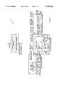
- FIG. 1is a block diagram of a digital communications system
- FIG. 2is a block diagram of a DBS receiver system comprising a tuner, an analog to digital converter, and a receiver chip;
- FIG. 3is a block diagram of a receiver chip comprising a demodulator stage, a convolutional decoder stage, and a de-interleaver/block decoder stage;
- FIG. 4is a block diagram of a module for providing a feedback signal from the receiver chip for clock acquisition and tracking.
- FIG. 2shows a DBS receiver system 10 comprising a tuner 12, an analog to digital converter 14, a receiver chip 16, and microprocessor 18.
- Tuner 12comprises frequency synthesizer 18, analog multiplier 20, intermediate frequency bandpass filter 22, gain control amplifier 24, automatic gain control loop filter 25, I/Q down converter 26, and voltage controlled oscillator 27.
- Tuner 12serves to convert a high frequency received signal to a baseband signal.
- Analog to digital converter 14serves to convert the analog baseband signal to a digital signal.
- Receiver chip 16serves to demodulate and decode the digital signal.
- the frequency synthesizeris set to be "tuned" to the high frequency received signal. This is accomplished by synthesizing an output signal 30 with a frequency which is offset by a fixed amount from the frequency of the desired received signal. The fixed amount will be the frequency of a product signal which is generated by multiplier 20.
- Multiplier 20multiplies high frequency signal 28 and output signal 30 from frequency synthesizer 18 to effectively shift the frequency of high frequency signal 28 to an intermediate frequency in an intermediate frequency signal.
- the product signal at the output of multiplier 20can be expressed as the sum of a desired intermediate frequency signal and other undesired byproduct signals.
- the product signalis coupled to intermediate frequency bandpass filter 22 which removes the undesired frequency components (and in so doing, removes the undesired byproduct signals) leaving only the intermediate frequency signal.
- Output of bandpass filter 22is coupled to gain control amplifier 24 which regulates the amplitude of the intermediate frequency signal.
- Gain control amplifier 24has an adaptive gain which is set to provide a constant amplitude output signal.
- the regulation mechanismis based on a negative feedback signal 32 provided by receiver chip 16. The effect of feedback signal 32 is to increase the gain of gain control amplifier 24 when the amplitude of the output signal declines below a target level, and to decrease the gain when the amplitude exceeds a target level.
- Output of the gain control amplifier 24is coupled to I/Q down converter 26 which converts the intermediate frequency signal to a baseband signal.
- the conversionmay take place in a similar fashion to the previous frequency conversion, but in this case two baseband signals are needed to represent the in-phase (I) and quadrature-phase (Q) components of the intermediate frequency signal.
- I/Q down converter 26regulates the offset error using negative feedback signal 34 provided by receiver chip 16. The effect of feedback signal 34 is to fine-tune the frequency of the local oscillator used in the down-conversion, thereby eliminating the residual oscillation.
- Output of I/Q down converter 26is coupled to analog to digital converter 14 which serves to convert the baseband signal to digital input signal 38.
- the rate at which the analog baseband signal is sampledis governed by a feedback signal 36.
- the feedback signalis initially set to provide a theoretically correct sampling frequency, and fine-tuned thereafter.
- the digital input signal 38is then coupled to receiver chip 16.
- FIG. 3shows receiver chip 16 comprising a demodulator stage 40, a convolutional decoder stage 42, and a de-interleaver and block decoder stage 46.
- Demodulator stage 40serves to provide filtering and symbol-rate sampling.
- Convolutional decoder stage 42serves as the first decoding stage of the concatenated decoder.
- the final decoding stageis provided by de-interleaver and block decoder stage 46.
- Demodulator stage 40comprises a matched filter 48 and a module 50 for timing control and gain control.
- Matched filter 48filters digital input signal 38 to substantially maximize the signal-to-noise ratio of the input signal.
- the impulse response of the filteris designed to be the time-reverse of the shape of a symbol signal. Hence, the filter is "matched" to the signal.
- One common symbol shapeis a square root raised cosine.
- Output of matched filter 48is coupled to module 50 which provides feedback signals for gain control 32, carrier synchronization 34, and clock synchronization 36.
- the feedback signal for gain controlis used to maintain a constant signal amplitude.
- the carrier synchronization feedback signalserves to fine-tune the local oscillator of the I/Q down converter to remove any residual oscillation.
- the clock synchronization feedback signalwill be treated in greater detail below.
- Demodulator stage 40may additionally comprise a decimation filter 52 and an output decimator 54.
- Decimation filter 52 and output decimator 54allow for oversampling by analog to digital converter 14. Oversampling is the practice of sampling an analog signal at a higher rate than the symbol rate. Use of this practice allows the transfer of some filtering operations from the analog domain to the digital domain. In general, only simple analog filters are practical. For complex filtering operations, digital filters are significantly easier to implement and adjust. By oversampling and performing the matched filter operation in the digital domain, a substantial implementation complexity reduction is achieved. Furthermore, the use of oversampling allows relaxed tolerances on the analog filters used in the analog-to-digital conversion process, without significant impairment to the signal-to-noise ratio. Demodulator stage 40 allows the rate of oversampling to be varied to accommodate differing data rates.
- the sampling rate of the signalPrior to the decoding stage, the sampling rate of the signal must be made equal to the symbol rate. This is accomplished through a digital lowpass filtering operation provided by decimation filter 52, and output decimator 54 which passes on only one sample per symbol.
- convolutional decoder stage 42comprises de-puncturing logic 56 and a Viterbi decoder 58.
- Viterbi decoder 58is a decoder for a standard industry convolutional code, namely a rate 1/2, constraint-length 7 code with octal generators (133, 171).
- Several well-known puncturing methodsare used to adapt this rate 1/2 code to a rate 2/3, 3/4, or 5/6 code which can still be decoded by the Viterbi decoder for the rate 1/2 code.
- De-puncturing logic 56performs the necessary adaptation on the receiving end.
- Viterbi synchronization circuit 60which relies on an estimation of the symbol error rate which can be determined from the output of comparator 62.
- Comparator 62determines the differences between the signal before decoding and a re-encoded version of the signal after decoding. Due to the error correcting capabilities of the Viterbi decoder, when only a few received symbol errors exist, the re-encoded signal should be relatively free of symbol errors. When the decoder is out of synchronization, the re-encoded signal will contain many symbol errors. Hence, the error rate determined by the comparator provides a good synchronization indicator.
- the output symbols from Viterbi decoder 58are coupled to de-interleaving and block decoding stage 46.
- De-interleaving and block decoding stage 46comprises synchronization circuit 66, de-interleaver 68, and block decoder 70.
- Synchronization circuit 66serves to locate the beginning of an interleaved code word block and forward data to de-interleaver 68 accordingly.
- De-interleaver 68 and block decoder 70are implemented with parameters specified in the digital video broadcast standard referenced previously.
- Synchronization circuit 66functions by scanning the Viterbi decoder output symbols for the sync bytes of 0047 hex. These bytes mark the beginning of a new block, and the synchronizer aligns the data accordingly for the subsequent de-interleaver and decoder.
- the output signal of synchronization circuit 66is coupled to de-interleaver 68.
- De-interleaver 68functions to disperse symbols which are adjacent in the output signal of synchronization circuit 66.
- the dispersionis the inverse of an interleave operation which was performed in the original encoding of the signal.
- One benefit of the dispersionis that it breaks up and isolates errors which are part of an error burst. This greatly benefits the performance of the block decoder.
- Block decoder 70performs the final error correction and decoding stage of the decoding process.
- a standard block code family used in these systemsis the family of Reed-Solomon codes. Reed-Solomon codes provide a powerful error correction ability which permits reliable decoding of the transmitted information.
- the decoded informationis then provided as output 39 from the DBS receiver system.
- FIG. 4shows a block diagram of a subsystem of module 50 which provides feedback signal 36 for clock synchronization.
- the clock synchronization circuit 72operates in one of two modes: acquisition and tracking.
- timing error detector 74measures characteristics of the signal output by matched filter 48 and provides a correction signal to accumulator 76 which provides a feedback signal representing a weighted sum of past correction signals.
- the feedback signalis buffered and amplified by amplifier 78.
- the feedback signalis then filtered by an off-chip, user configurable filter 80 and coupled to voltage controlled oscillator 82 as shown. Voltage controlled oscillator 82 is used to provide the clock for analog to digital converter 14, thereby closing the phase-locked loop.
- phase-locked loopsA well-known property of phase-locked loops is inordinate non-linearity. For correct operation, phase-locked loops must first be placed in an initial state closely approximating the correct operating point. In the acquisition mode automatic frequency controller 84 serves this function.
- Automatic frequency controller 84uses a counter and a timer comprised of a second counter and a crystal oscillator 86 to determine the output frequency of voltage controlled oscillator 82.
- automatic frequency controllerloads the second counter and decrements it for every clock cycle of crystal oscillator 86 until the counter reaches zero.
- the second counteris loaded, the first counter is also loaded with the desired number of oscillations of voltage controlled oscillator 82 in the timer interval.
- the first counteris decremented for every oscillation of voltage controlled oscillator 82.
- the contents of the first counterare inspected.
- the advantages of the receiver system detailed aboveinclude a reduced part count.
- the novel clock synchronization circuitpermits the use of a single voltage controlled oscillator for clocking the analog-to-digital converter.
- itis necessary to use a bank of multiple voltage controlled crystal oscillators which are more accurate (and expensive) but have a sharply reduced range of oscillation.
- This advantageis gained through the use of digitally controlled feedback by the automatic frequency controller during the initial timing acquisition stage.
- An additional reduction in part countarises from the combination of the demodulation and decoding stages onto a single chip.
- the overall part count reductionleads to a significant simplification of board layout. Consequently a sharply increased reliability and hence increased utility are also obtained.
Landscapes
- Engineering & Computer Science (AREA)
- Signal Processing (AREA)
- Computer Networks & Wireless Communication (AREA)
- Physics & Mathematics (AREA)
- Astronomy & Astrophysics (AREA)
- General Physics & Mathematics (AREA)
- Artificial Intelligence (AREA)
- Digital Transmission Methods That Use Modulated Carrier Waves (AREA)
- Error Detection And Correction (AREA)
Abstract
Description
Claims (15)
Priority Applications (2)
| Application Number | Priority Date | Filing Date | Title |
|---|---|---|---|
| US08/741,269US5953636A (en) | 1996-10-30 | 1996-10-30 | Single-chip DBS receiver |
| PCT/US1997/019292WO1998019408A2 (en) | 1996-10-30 | 1997-10-24 | Single-chip dbs receiver |
Applications Claiming Priority (1)
| Application Number | Priority Date | Filing Date | Title |
|---|---|---|---|
| US08/741,269US5953636A (en) | 1996-10-30 | 1996-10-30 | Single-chip DBS receiver |
Publications (1)
| Publication Number | Publication Date |
|---|---|
| US5953636Atrue US5953636A (en) | 1999-09-14 |
Family
ID=24980043
Family Applications (1)
| Application Number | Title | Priority Date | Filing Date |
|---|---|---|---|
| US08/741,269Expired - LifetimeUS5953636A (en) | 1996-10-30 | 1996-10-30 | Single-chip DBS receiver |
Country Status (2)
| Country | Link |
|---|---|
| US (1) | US5953636A (en) |
| WO (1) | WO1998019408A2 (en) |
Cited By (28)
| Publication number | Priority date | Publication date | Assignee | Title |
|---|---|---|---|---|
| US6038253A (en)* | 1995-09-18 | 2000-03-14 | Oki Electric Industry Co., Ltd. | Data receiver with symbol rate discrimination and statistical analysis functions |
| US6133965A (en)* | 1998-02-12 | 2000-10-17 | Zenith Electronics Corporation | Digital AGC control for high definition television tuner |
| US6205188B1 (en)* | 1997-05-02 | 2001-03-20 | Lsi Logic Corporation | Demodulating digital video broadcast signals |
| DE19948898A1 (en)* | 1999-10-11 | 2001-05-23 | Infineon Technologies Ag | Digital filter combination |
| US6275540B1 (en)* | 1997-10-01 | 2001-08-14 | Motorola, Inc. | Selective call receiver having an apparatus for modifying an analog signal to a digital signal and method therefor |
| US20020018147A1 (en)* | 2000-07-03 | 2002-02-14 | Alps Electric Co., Ltd. | Television tuner for reducing power consumption and video device using the television tuner |
| US20020071653A1 (en)* | 2000-10-06 | 2002-06-13 | Cowley Nicholas Paul | Tuner |
| US20020158992A1 (en)* | 2000-02-08 | 2002-10-31 | Yeo Alan Chin Leong | Automatic gain control |
| US6639954B2 (en)* | 1998-05-28 | 2003-10-28 | Fujitsu Limited | Mobile communication terminal and transmission-bit-rate detection method |
| US6714608B1 (en)* | 1998-01-27 | 2004-03-30 | Broadcom Corporation | Multi-mode variable rate digital satellite receiver |
| US20040252245A1 (en)* | 2003-04-11 | 2004-12-16 | Stmicroelectronics S.A. | Electronic component allowing the decoding of digital terrestrial or cable television signals |
| US20040259512A1 (en)* | 2003-04-11 | 2004-12-23 | Stmicroelectronics S.A. | Electronic component with integrated tuning device, allowing the decoding of digital terrestrial or cable television signals |
| US20040257480A1 (en)* | 2003-04-03 | 2004-12-23 | Stmicroelectronics S.A. | Electronic component allowing the decoding of digital terrestrial or cable television signals |
| US20040268396A1 (en)* | 2003-04-01 | 2004-12-30 | Stmicroelectronics S.A. | Electronic component allowing the decoding of satellite digital television signals |
| US20050071877A1 (en)* | 2003-09-25 | 2005-03-31 | Navarro Efren N. | Satellite downstream porting interface API |
| US20050179487A1 (en)* | 2004-02-17 | 2005-08-18 | Wai Lee | Switching power amplifier using a frequency translating delta sigma modulator |
| US6944121B1 (en) | 2001-03-19 | 2005-09-13 | Cisco Systems Wireless Networking (Australia) Pty Limited | Wireless computer network including a mobile appliance containing a single chip transceiver |
| US6950643B1 (en) | 1999-10-11 | 2005-09-27 | Infineon Technologies Ag | Digital filter combination |
| US20050229217A1 (en)* | 2004-03-29 | 2005-10-13 | Broadcom Corporation | Method and system for downstream time stamp in an adaptive modulation based satellite modem termination system |
| US7110381B1 (en) | 2001-03-19 | 2006-09-19 | Cisco Systems Wireless Networking (Australia) Pty Limited | Diversity transceiver for a wireless local area network |
| US20060210002A1 (en)* | 2005-03-03 | 2006-09-21 | Xueshi Yang | Timing recovery in a parallel channel communication system |
| US20080026717A1 (en)* | 2006-07-31 | 2008-01-31 | Phuong T. Huynh | Bandpass-sampling delta-sigma communication receiver |
| US20080062601A1 (en)* | 2006-08-31 | 2008-03-13 | Texas Instruments | Magnetic techniques to address electrostatic discharge |
| US20100097261A1 (en)* | 2008-10-22 | 2010-04-22 | Mediatek Inc. | Digitizer with variable sampling clock and method using the same |
| US8693591B1 (en) | 2012-09-20 | 2014-04-08 | Phuong Huynh | Apparatus and method for tuning the frequency of a bandpass filter to an offset frequency around a carrier frequency |
| US8717212B2 (en) | 2012-09-20 | 2014-05-06 | Phuong Huynh | Bandpass-sampling delta-sigma demodulator |
| US8816781B2 (en) | 2012-09-20 | 2014-08-26 | Phuong Huynh | Apparatus and method to detect frequency difference |
| US9396062B1 (en)* | 2014-04-04 | 2016-07-19 | Seagate Technology Llc | Group based codes for multi-dimensional recording (MDR) |
Citations (27)
| Publication number | Priority date | Publication date | Assignee | Title |
|---|---|---|---|---|
| US4261054A (en)* | 1977-12-15 | 1981-04-07 | Harris Corporation | Real-time adaptive power control in satellite communications systems |
| US4641324A (en)* | 1984-09-14 | 1987-02-03 | Eastman Kodak Company | Signal correction apparatus |
| US4694291A (en)* | 1985-02-07 | 1987-09-15 | Alcatel | Device for transmitting a clock signal accompanied by a synchronization signal |
| US4829525A (en)* | 1986-10-24 | 1989-05-09 | Mitsubishi Denki Kabushiki Kaisha | PCM signal reproducing apparatus including error/erasure correction circuit |
| US4845713A (en)* | 1987-06-08 | 1989-07-04 | Exabyte Corporation | Method and apparatus for determining the coefficients of a locator polynomial |
| US4928288A (en)* | 1987-12-22 | 1990-05-22 | Societa' Italiana per L'Esercizio Delle Telecomunicazioni P.A. | Decoding method and device with erasure detection for multilevel transmission systems |
| US5051998A (en)* | 1988-06-28 | 1991-09-24 | Matsushita Electric Industrial Co., Ltd. | Data block deinterleaving and error correction system |
| US5088113A (en)* | 1990-01-02 | 1992-02-11 | At&T Bell Laboratories | Diversity coded modulation |
| EP0501829A1 (en)* | 1991-02-28 | 1992-09-02 | Texas Instruments Incorporated | System and method for a digital navigation satellite receiver |
| US5181209A (en)* | 1989-04-03 | 1993-01-19 | Deutsche Forschungsanstalt Fur Luft- Und Raumfahrt E.V. | Method for generalizing the viterbi algorithm and devices for executing the method |
| US5216677A (en)* | 1989-09-20 | 1993-06-01 | Matsushita Electric Industrial Co., Ltd. | Data reproducing apparatus |
| US5276904A (en)* | 1989-07-04 | 1994-01-04 | Thomson Composants Microondes | System for receiving TV signals retransmitted by satellites |
| DE4237692C1 (en)* | 1992-11-07 | 1994-03-03 | Grundig Emv | Receiver for a digital broadcast signal |
| US5390195A (en)* | 1992-04-03 | 1995-02-14 | Ampex Corporation | Miller-squared decoder with erasure flag output |
| US5420640A (en)* | 1993-12-03 | 1995-05-30 | Scientific-Atlanta, Inc. | Memory efficient method and apparatus for sync detection |
| US5422894A (en)* | 1993-06-25 | 1995-06-06 | Oki Electric Industry Co., Ltd. | Real-time convolutional decoder with block synchronizing function |
| US5430743A (en)* | 1993-06-29 | 1995-07-04 | Motorola, Inc. | Method and apparatus for recovering data in a radio communication system |
| US5457704A (en)* | 1993-05-21 | 1995-10-10 | At&T Ipm Corp. | Post processing method and apparatus for symbol reliability generation |
| EP0696854A1 (en)* | 1994-08-08 | 1996-02-14 | THOMSON multimedia S.A. | Broadcast receiver adapted for analog and digital signals |
| WO1996012352A1 (en)* | 1994-10-13 | 1996-04-25 | Westinghouse Electric Corporation | Mobile terminal apparatus for a satellite communication system |
| US5517529A (en)* | 1993-10-18 | 1996-05-14 | Westinghouse Electric Corp. | UHF/L-Band monolithic direct digital receiver |
| US5519734A (en)* | 1994-08-15 | 1996-05-21 | Lsi Logic Corporation | Synchronization arrangement for decoder-de-interleaver |
| EP0716518A2 (en)* | 1994-12-08 | 1996-06-12 | Broadcom Corporation | Narrow-band quadrature demodulator for digital audio broadcast via satellite |
| US5548684A (en)* | 1994-04-22 | 1996-08-20 | Georgia Tech Research Corporation | Artificial neural network viterbi decoding system and method |
| US5706665A (en)* | 1996-06-04 | 1998-01-13 | Super S.E.E.R. Systems Inc. | Refrigeration system |
| US5708665A (en)* | 1996-08-22 | 1998-01-13 | Lsi Logic Corporation | Digital receiver using equalization and block decoding with erasure and error correction |
| US5710783A (en)* | 1995-06-07 | 1998-01-20 | Luthi; Daniel A. | Optimization of synchronization control in concatenated decoders |
- 1996
- 1996-10-30USUS08/741,269patent/US5953636A/ennot_activeExpired - Lifetime
- 1997
- 1997-10-24WOPCT/US1997/019292patent/WO1998019408A2/enactiveApplication Filing
Patent Citations (28)
| Publication number | Priority date | Publication date | Assignee | Title |
|---|---|---|---|---|
| US4261054A (en)* | 1977-12-15 | 1981-04-07 | Harris Corporation | Real-time adaptive power control in satellite communications systems |
| US4641324A (en)* | 1984-09-14 | 1987-02-03 | Eastman Kodak Company | Signal correction apparatus |
| US4694291A (en)* | 1985-02-07 | 1987-09-15 | Alcatel | Device for transmitting a clock signal accompanied by a synchronization signal |
| US4829525A (en)* | 1986-10-24 | 1989-05-09 | Mitsubishi Denki Kabushiki Kaisha | PCM signal reproducing apparatus including error/erasure correction circuit |
| US4845713A (en)* | 1987-06-08 | 1989-07-04 | Exabyte Corporation | Method and apparatus for determining the coefficients of a locator polynomial |
| US4928288A (en)* | 1987-12-22 | 1990-05-22 | Societa' Italiana per L'Esercizio Delle Telecomunicazioni P.A. | Decoding method and device with erasure detection for multilevel transmission systems |
| US5051998A (en)* | 1988-06-28 | 1991-09-24 | Matsushita Electric Industrial Co., Ltd. | Data block deinterleaving and error correction system |
| US5181209A (en)* | 1989-04-03 | 1993-01-19 | Deutsche Forschungsanstalt Fur Luft- Und Raumfahrt E.V. | Method for generalizing the viterbi algorithm and devices for executing the method |
| US5276904A (en)* | 1989-07-04 | 1994-01-04 | Thomson Composants Microondes | System for receiving TV signals retransmitted by satellites |
| US5216677A (en)* | 1989-09-20 | 1993-06-01 | Matsushita Electric Industrial Co., Ltd. | Data reproducing apparatus |
| US5088113A (en)* | 1990-01-02 | 1992-02-11 | At&T Bell Laboratories | Diversity coded modulation |
| EP0501829A1 (en)* | 1991-02-28 | 1992-09-02 | Texas Instruments Incorporated | System and method for a digital navigation satellite receiver |
| US5390195A (en)* | 1992-04-03 | 1995-02-14 | Ampex Corporation | Miller-squared decoder with erasure flag output |
| DE4237692C1 (en)* | 1992-11-07 | 1994-03-03 | Grundig Emv | Receiver for a digital broadcast signal |
| US5457704A (en)* | 1993-05-21 | 1995-10-10 | At&T Ipm Corp. | Post processing method and apparatus for symbol reliability generation |
| US5422894A (en)* | 1993-06-25 | 1995-06-06 | Oki Electric Industry Co., Ltd. | Real-time convolutional decoder with block synchronizing function |
| US5430743A (en)* | 1993-06-29 | 1995-07-04 | Motorola, Inc. | Method and apparatus for recovering data in a radio communication system |
| US5517529A (en)* | 1993-10-18 | 1996-05-14 | Westinghouse Electric Corp. | UHF/L-Band monolithic direct digital receiver |
| US5420640A (en)* | 1993-12-03 | 1995-05-30 | Scientific-Atlanta, Inc. | Memory efficient method and apparatus for sync detection |
| US5548684A (en)* | 1994-04-22 | 1996-08-20 | Georgia Tech Research Corporation | Artificial neural network viterbi decoding system and method |
| EP0696854A1 (en)* | 1994-08-08 | 1996-02-14 | THOMSON multimedia S.A. | Broadcast receiver adapted for analog and digital signals |
| US5519734A (en)* | 1994-08-15 | 1996-05-21 | Lsi Logic Corporation | Synchronization arrangement for decoder-de-interleaver |
| WO1996012352A1 (en)* | 1994-10-13 | 1996-04-25 | Westinghouse Electric Corporation | Mobile terminal apparatus for a satellite communication system |
| EP0716518A2 (en)* | 1994-12-08 | 1996-06-12 | Broadcom Corporation | Narrow-band quadrature demodulator for digital audio broadcast via satellite |
| US5640670A (en)* | 1994-12-08 | 1997-06-17 | Broadcom Corporation | Narrow-band quadrature demodulator for recovering analog video and digital audio in a direct broadcast system |
| US5710783A (en)* | 1995-06-07 | 1998-01-20 | Luthi; Daniel A. | Optimization of synchronization control in concatenated decoders |
| US5706665A (en)* | 1996-06-04 | 1998-01-13 | Super S.E.E.R. Systems Inc. | Refrigeration system |
| US5708665A (en)* | 1996-08-22 | 1998-01-13 | Lsi Logic Corporation | Digital receiver using equalization and block decoding with erasure and error correction |
Non-Patent Citations (22)
| Title |
|---|
| Arazi, B, "A Commonsense Approach to the Theory of Error Correcting Codes", The MIT Press, 1988, p. 137. |
| Arazi, B, A Commonsense Approach to the Theory of Error Correcting Codes , The MIT Press, 1988, p. 137.* |
| Chien et al., Monolithic GPS Receiver and Synthesizer Using High Speed Silicon Bipolar Technology, IEEE, pp. 64 67, Feb. 1992.* |
| Chien et al., Monolithic GPS Receiver and Synthesizer Using High-Speed Silicon Bipolar Technology, IEEE, pp. 64-67, Feb. 1992. |
| Deng, R., et al, "High Rate Concatenated Coding Systems Using Bandwidth Efficient Trellis Inner Codes" IEEE Transactions on Communications, vol. 37, No. 5, May 1989., pp. 420-426. |
| Deng, R., et al, "High Rate Concatenated Coding Systems Using Multidimensional Bandwidth-Efficient Trellis Inner Codes," IEEE Transactions on Communications, vol. 37, No. 10, Oct. 1989, pp. 1091-1095. |
| Deng, R., et al, High Rate Concatenated Coding Systems Using Bandwidth Efficient Trellis Inner Codes IEEE Transactions on Communications, vol. 37, No. 5, May 1989., pp. 420 426.* |
| Deng, R., et al, High Rate Concatenated Coding Systems Using Multidimensional Bandwidth Efficient Trellis Inner Codes, IEEE Transactions on Communications, vol. 37, No. 10, Oct. 1989, pp. 1091 1095.* |
| Hagenauer, J., "Forward Error Correction Coding for Fading Compensation in Mobile Satellite Channels", IEEE Journal on Selected Areas in Communications, vol. SAC-5, No. 2, Feb. 1987, pp. 215-225. |
| Hagenauer, J., et al, "A Viterbi Algorithm with Soft-Decision Outputs and its Applications," IEEE CH2682-3/89/0000-1680, pp. 1680-1686. |
| Hagenauer, J., et al, A Viterbi Algorithm with Soft Decision Outputs and its Applications, IEEE CH2682 3/89/0000 1680, pp. 1680 1686.* |
| Hagenauer, J., Forward Error Correction Coding for Fading Compensation in Mobile Satellite Channels , IEEE Journal on Selected Areas in Communications, vol. SAC 5, No. 2, Feb. 1987, pp. 215 225.* |
| Hubbard et al, A Family of Low Cost High Performance HEMT MMICs for Commercial DBS Applications, IEEE, pp. 133 136, 1995.* |
| Hubbard et al, A Family of Low Cost High Performance HEMT MMICs for Commercial DBS Applications, IEEE, pp. 133-136, 1995. |
| Koshelets et al, Integrated Sub MM Wave Receivers, IEEE, pp. 3057 3060, Jun. 1995.* |
| Koshelets et al, Integrated Sub-MM Wave Receivers, IEEE, pp. 3057-3060, Jun. 1995. |
| Oppenheim, et al, Discrete Time Signal Processing , 1989 by Prentice Hall, pp. 444 448.* |
| Oppenheim, et al, Discrete-Time Signal Processing, 1989 by Prentice Hall, pp. 444-448. |
| Sklar, Bernard, Digital Communications: Fundamentals and Applications , 1988 by Prentice Hall, pp. 263 265.* |
| Sklar, Bernard, Digital Communications: Fundamentals and Applications, 1988 by Prentice Hall, pp. 263-265. |
| Whitaker, S. et al., "Reed Solomon VLSI Codec for Advanced Television", IEEE Transactions on Circuits and Systems for Video Technology, vol. 1, No. 2, Jun. 1991, pp. 230-236. |
| Whitaker, S. et al., Reed Solomon VLSI Codec for Advanced Television , IEEE Transactions on Circuits and Systems for Video Technology, vol. 1, No. 2, Jun. 1991, pp. 230 236.* |
Cited By (55)
| Publication number | Priority date | Publication date | Assignee | Title |
|---|---|---|---|---|
| US6038253A (en)* | 1995-09-18 | 2000-03-14 | Oki Electric Industry Co., Ltd. | Data receiver with symbol rate discrimination and statistical analysis functions |
| US6205188B1 (en)* | 1997-05-02 | 2001-03-20 | Lsi Logic Corporation | Demodulating digital video broadcast signals |
| US6628730B1 (en) | 1997-05-02 | 2003-09-30 | Lsi Logic Corporation | Demodulating digital video broadcast signals |
| US6275540B1 (en)* | 1997-10-01 | 2001-08-14 | Motorola, Inc. | Selective call receiver having an apparatus for modifying an analog signal to a digital signal and method therefor |
| US20040151263A1 (en)* | 1998-01-27 | 2004-08-05 | Broadcom Corporation | Multi-mode variable rate digital satellite receiver |
| US7302013B2 (en) | 1998-01-27 | 2007-11-27 | Broadcom Corporation | Multi-mode variable rate digital satellite receiver |
| US6714608B1 (en)* | 1998-01-27 | 2004-03-30 | Broadcom Corporation | Multi-mode variable rate digital satellite receiver |
| US6133965A (en)* | 1998-02-12 | 2000-10-17 | Zenith Electronics Corporation | Digital AGC control for high definition television tuner |
| US6639954B2 (en)* | 1998-05-28 | 2003-10-28 | Fujitsu Limited | Mobile communication terminal and transmission-bit-rate detection method |
| DE19948898A1 (en)* | 1999-10-11 | 2001-05-23 | Infineon Technologies Ag | Digital filter combination |
| DE19948898B4 (en)* | 1999-10-11 | 2006-01-12 | Infineon Technologies Ag | Digital filter combination |
| US6950643B1 (en) | 1999-10-11 | 2005-09-27 | Infineon Technologies Ag | Digital filter combination |
| US20020158992A1 (en)* | 2000-02-08 | 2002-10-31 | Yeo Alan Chin Leong | Automatic gain control |
| US7002638B2 (en)* | 2000-02-08 | 2006-02-21 | Koninklijke Philips Electronics N.V. | Automatic gain control |
| US6757028B2 (en)* | 2000-07-03 | 2004-06-29 | Alps Electric Co., Ltd. | Television tuner for reducing power consumption and video device using the television tuner |
| US20020018147A1 (en)* | 2000-07-03 | 2002-02-14 | Alps Electric Co., Ltd. | Television tuner for reducing power consumption and video device using the television tuner |
| US20020071653A1 (en)* | 2000-10-06 | 2002-06-13 | Cowley Nicholas Paul | Tuner |
| US7006162B2 (en)* | 2000-10-06 | 2006-02-28 | Zarlink Semiconductor Limited | Tuner |
| US7110381B1 (en) | 2001-03-19 | 2006-09-19 | Cisco Systems Wireless Networking (Australia) Pty Limited | Diversity transceiver for a wireless local area network |
| US6944121B1 (en) | 2001-03-19 | 2005-09-13 | Cisco Systems Wireless Networking (Australia) Pty Limited | Wireless computer network including a mobile appliance containing a single chip transceiver |
| US20050237924A1 (en)* | 2001-03-19 | 2005-10-27 | Neil Weste | Wireless computer network inluding a mobile appliance containing a single chip transceiver |
| US20070049348A1 (en)* | 2001-03-19 | 2007-03-01 | O'sullivan John | Diversity transceiver for a wireless local area network |
| US7636344B2 (en) | 2001-03-19 | 2009-12-22 | Cisco Technology, Inc. | Diversity transceiver for a wireless local area network |
| US7164651B2 (en) | 2001-03-19 | 2007-01-16 | Cisco Systems Wireless Networking (Australia) Pty Limited | Wireless computer network including a mobile appliance containing a single chip transceiver |
| US7061855B2 (en) | 2001-03-19 | 2006-06-13 | Cisco Systems Wireless Networking (Australia) Pty Limited | Wireless computer network including a mobile appliance containing a single chip transceiver |
| US20060194614A1 (en)* | 2001-03-19 | 2006-08-31 | Neil Weste | Wireless computer network inluding a mobile appliance containing a single chip transceiver |
| US7643634B2 (en) | 2003-04-01 | 2010-01-05 | Stmicroelectronics S.A. | Electronic component allowing the decoding of satellite digital television signals |
| US20040268396A1 (en)* | 2003-04-01 | 2004-12-30 | Stmicroelectronics S.A. | Electronic component allowing the decoding of satellite digital television signals |
| US20040257480A1 (en)* | 2003-04-03 | 2004-12-23 | Stmicroelectronics S.A. | Electronic component allowing the decoding of digital terrestrial or cable television signals |
| US7962949B2 (en)* | 2003-04-03 | 2011-06-14 | Stmicroelectronics S.A. | Electronic component allowing the decoding of digital terrestrial or cable television signals |
| US20040252245A1 (en)* | 2003-04-11 | 2004-12-16 | Stmicroelectronics S.A. | Electronic component allowing the decoding of digital terrestrial or cable television signals |
| US7406304B2 (en) | 2003-04-11 | 2008-07-29 | Stmicroelectronics S.A. | Electronic component with integrated tuning device, allowing the decoding of digital terrestrial or cable television signals |
| US20040259512A1 (en)* | 2003-04-11 | 2004-12-23 | Stmicroelectronics S.A. | Electronic component with integrated tuning device, allowing the decoding of digital terrestrial or cable television signals |
| US7796197B2 (en)* | 2003-04-11 | 2010-09-14 | Stmicroelectronics S.A. | Electronic component allowing the decoding of digital terrestrial or cable television signals |
| US20050071877A1 (en)* | 2003-09-25 | 2005-03-31 | Navarro Efren N. | Satellite downstream porting interface API |
| US20050179487A1 (en)* | 2004-02-17 | 2005-08-18 | Wai Lee | Switching power amplifier using a frequency translating delta sigma modulator |
| GB2427775B (en)* | 2004-02-17 | 2007-12-27 | Pulsewave Rf Inc | Switching power amplifier using a frequency translating delta sigma modulator |
| WO2005079240A3 (en)* | 2004-02-17 | 2005-12-15 | Prophesi Technologies Inc | Switching power amplifier using a frequency translating delta sigma modulator |
| US7023267B2 (en)* | 2004-02-17 | 2006-04-04 | Prophesi Technologies, Inc. | Switching power amplifier using a frequency translating delta sigma modulator |
| GB2427775A (en)* | 2004-02-17 | 2007-01-03 | Pulsewave Rf Inc | Switching power amplifier using a frequency translating delta sigma modulator |
| US7992174B2 (en)* | 2004-03-29 | 2011-08-02 | Broadcom Corporation | Method and system for downstream time stamp in an adaptive modulation based satellite modem termination system |
| US20050229217A1 (en)* | 2004-03-29 | 2005-10-13 | Broadcom Corporation | Method and system for downstream time stamp in an adaptive modulation based satellite modem termination system |
| US20060210002A1 (en)* | 2005-03-03 | 2006-09-21 | Xueshi Yang | Timing recovery in a parallel channel communication system |
| US7889823B2 (en)* | 2005-03-03 | 2011-02-15 | Seagate Technology Llc | Timing recovery in a parallel channel communication system |
| US20080026717A1 (en)* | 2006-07-31 | 2008-01-31 | Phuong T. Huynh | Bandpass-sampling delta-sigma communication receiver |
| US7643259B2 (en)* | 2006-08-31 | 2010-01-05 | Texas Instruments Incorporated | Substrate, with ESD magnetically induced wires, bound to passives/product ICS |
| US20080062601A1 (en)* | 2006-08-31 | 2008-03-13 | Texas Instruments | Magnetic techniques to address electrostatic discharge |
| US7808419B2 (en)* | 2008-10-22 | 2010-10-05 | Mediatek Inc. | Digitizer with variable sampling clock and method using the same |
| US20100321576A1 (en)* | 2008-10-22 | 2010-12-23 | Mediatek Inc. | Digitizer with Variable Sampling Clock and Method Using the Same |
| US20100097261A1 (en)* | 2008-10-22 | 2010-04-22 | Mediatek Inc. | Digitizer with variable sampling clock and method using the same |
| US8031103B2 (en) | 2008-10-22 | 2011-10-04 | Mediatek Inc. | Digitizer with variable sampling clock and method using the same |
| US8693591B1 (en) | 2012-09-20 | 2014-04-08 | Phuong Huynh | Apparatus and method for tuning the frequency of a bandpass filter to an offset frequency around a carrier frequency |
| US8717212B2 (en) | 2012-09-20 | 2014-05-06 | Phuong Huynh | Bandpass-sampling delta-sigma demodulator |
| US8816781B2 (en) | 2012-09-20 | 2014-08-26 | Phuong Huynh | Apparatus and method to detect frequency difference |
| US9396062B1 (en)* | 2014-04-04 | 2016-07-19 | Seagate Technology Llc | Group based codes for multi-dimensional recording (MDR) |
Also Published As
| Publication number | Publication date |
|---|---|
| WO1998019408A2 (en) | 1998-05-07 |
| WO1998019408A3 (en) | 1998-09-17 |
Similar Documents
| Publication | Publication Date | Title |
|---|---|---|
| US5953636A (en) | Single-chip DBS receiver | |
| RU2171548C2 (en) | Device for decoding video signals coded in different formats | |
| EP0813345B1 (en) | Digital demodulator and method therefor | |
| US6888888B1 (en) | Simultaneous tuning of multiple channels using intermediate frequency sub-sampling | |
| D'Amico et al. | Efficient non-data-aided carrier and clock recovery for satellite DVB at very low signal-to-noise ratios | |
| US6134282A (en) | Method for lowpass filter calibration in a satellite receiver | |
| US5819157A (en) | Reduced power tuner chip with integrated voltage regulator for a satellite receiver system | |
| EP0574273B1 (en) | A receiver compriser a combined AM-FM demodulator | |
| US5999793A (en) | Satellite receiver tuner chip with frequency synthesizer having an externally configurable charge pump | |
| US7724833B2 (en) | Receiver for an LDPC based TDS-OFDM communication system | |
| EP0769873A1 (en) | Radio frequency receiver adapted to receive one or more modulated signals | |
| US6545728B1 (en) | Digital television receivers that digitize final I-F signals resulting from triple-conversion | |
| US6301312B1 (en) | Bandpass phase tracker with hilbert transformation before analog-to-digital conversion | |
| MXPA98000366A (en) | Device for decoding video signals coded in different way | |
| US20030193618A1 (en) | Radio receiver for receiving both vsb and qam digital hdtv signals | |
| EP1716682A1 (en) | Method and apparatus for carrier recovery in a communications system | |
| KR100348259B1 (en) | VSB receiver | |
| US5812927A (en) | System and method for correction of I/Q angular error in a satellite receiver | |
| JPH0678014A (en) | Television signal processor | |
| US6714262B1 (en) | Channel selection device for receiving digital TV broadcasting, receiving device and channel selection method | |
| US6665355B1 (en) | Method and apparatus for pilot-aided carrier acquisition of vestigial sideband signal | |
| US7688923B2 (en) | Enhanced data rate receiver | |
| US5995563A (en) | System and method for fast channel switching in a satellite receiver | |
| KR100260421B1 (en) | Digital receiver with march filter responsive to field synchronization code in the final i-f signal envelope | |
| CN1157943C (en) | Selective gain adjustement to aid carrier acquisition in a high definition television receiver |
Legal Events
| Date | Code | Title | Description |
|---|---|---|---|
| AS | Assignment | Owner name:LSI LOGIC CORPORATION, CALIFORNIA Free format text:ASSIGNMENT OF ASSIGNORS INTEREST;ASSIGNORS:KEATE, CHRISTOPHER;LUTHI, DANIEL;REEL/FRAME:008477/0062 Effective date:19970115 | |
| STCF | Information on status: patent grant | Free format text:PATENTED CASE | |
| FPAY | Fee payment | Year of fee payment:4 | |
| FPAY | Fee payment | Year of fee payment:8 | |
| FEPP | Fee payment procedure | Free format text:PAYER NUMBER DE-ASSIGNED (ORIGINAL EVENT CODE: RMPN); ENTITY STATUS OF PATENT OWNER: LARGE ENTITY Free format text:PAYOR NUMBER ASSIGNED (ORIGINAL EVENT CODE: ASPN); ENTITY STATUS OF PATENT OWNER: LARGE ENTITY | |
| FPAY | Fee payment | Year of fee payment:12 | |
| AS | Assignment | Owner name:DEUTSCHE BANK AG NEW YORK BRANCH, AS COLLATERAL AG Free format text:PATENT SECURITY AGREEMENT;ASSIGNORS:LSI CORPORATION;AGERE SYSTEMS LLC;REEL/FRAME:032856/0031 Effective date:20140506 | |
| AS | Assignment | Owner name:LSI CORPORATION, CALIFORNIA Free format text:CHANGE OF NAME;ASSIGNOR:LSI LOGIC CORPORATION;REEL/FRAME:033102/0270 Effective date:20070406 | |
| AS | Assignment | Owner name:AVAGO TECHNOLOGIES GENERAL IP (SINGAPORE) PTE. LTD Free format text:ASSIGNMENT OF ASSIGNORS INTEREST;ASSIGNOR:LSI CORPORATION;REEL/FRAME:035390/0388 Effective date:20140814 | |
| AS | Assignment | Owner name:AGERE SYSTEMS LLC, PENNSYLVANIA Free format text:TERMINATION AND RELEASE OF SECURITY INTEREST IN PATENT RIGHTS (RELEASES RF 032856-0031);ASSIGNOR:DEUTSCHE BANK AG NEW YORK BRANCH, AS COLLATERAL AGENT;REEL/FRAME:037684/0039 Effective date:20160201 Owner name:LSI CORPORATION, CALIFORNIA Free format text:TERMINATION AND RELEASE OF SECURITY INTEREST IN PATENT RIGHTS (RELEASES RF 032856-0031);ASSIGNOR:DEUTSCHE BANK AG NEW YORK BRANCH, AS COLLATERAL AGENT;REEL/FRAME:037684/0039 Effective date:20160201 | |
| AS | Assignment | Owner name:BANK OF AMERICA, N.A., AS COLLATERAL AGENT, NORTH CAROLINA Free format text:PATENT SECURITY AGREEMENT;ASSIGNOR:AVAGO TECHNOLOGIES GENERAL IP (SINGAPORE) PTE. LTD.;REEL/FRAME:037808/0001 Effective date:20160201 Owner name:BANK OF AMERICA, N.A., AS COLLATERAL AGENT, NORTH Free format text:PATENT SECURITY AGREEMENT;ASSIGNOR:AVAGO TECHNOLOGIES GENERAL IP (SINGAPORE) PTE. LTD.;REEL/FRAME:037808/0001 Effective date:20160201 | |
| AS | Assignment | Owner name:AVAGO TECHNOLOGIES GENERAL IP (SINGAPORE) PTE. LTD., SINGAPORE Free format text:TERMINATION AND RELEASE OF SECURITY INTEREST IN PATENTS;ASSIGNOR:BANK OF AMERICA, N.A., AS COLLATERAL AGENT;REEL/FRAME:041710/0001 Effective date:20170119 Owner name:AVAGO TECHNOLOGIES GENERAL IP (SINGAPORE) PTE. LTD Free format text:TERMINATION AND RELEASE OF SECURITY INTEREST IN PATENTS;ASSIGNOR:BANK OF AMERICA, N.A., AS COLLATERAL AGENT;REEL/FRAME:041710/0001 Effective date:20170119 |