US5953615A - Pre-amorphization process for source/drain junction - Google Patents
Pre-amorphization process for source/drain junctionDownload PDFInfo
- Publication number
- US5953615A US5953615AUS09/238,359US23835999AUS5953615AUS 5953615 AUS5953615 AUS 5953615AUS 23835999 AUS23835999 AUS 23835999AUS 5953615 AUS5953615 AUS 5953615A
- Authority
- US
- United States
- Prior art keywords
- amorphous regions
- deep
- shallow
- source
- ions
- Prior art date
- Legal status (The legal status is an assumption and is not a legal conclusion. Google has not performed a legal analysis and makes no representation as to the accuracy of the status listed.)
- Expired - Lifetime
Links
Images

Classifications
- H—ELECTRICITY
- H01—ELECTRIC ELEMENTS
- H01L—SEMICONDUCTOR DEVICES NOT COVERED BY CLASS H10
- H01L21/00—Processes or apparatus adapted for the manufacture or treatment of semiconductor or solid state devices or of parts thereof
- H01L21/02—Manufacture or treatment of semiconductor devices or of parts thereof
- H01L21/04—Manufacture or treatment of semiconductor devices or of parts thereof the devices having potential barriers, e.g. a PN junction, depletion layer or carrier concentration layer
- H01L21/18—Manufacture or treatment of semiconductor devices or of parts thereof the devices having potential barriers, e.g. a PN junction, depletion layer or carrier concentration layer the devices having semiconductor bodies comprising elements of Group IV of the Periodic Table or AIIIBV compounds with or without impurities, e.g. doping materials
- H01L21/26—Bombardment with radiation
- H01L21/263—Bombardment with radiation with high-energy radiation
- H01L21/265—Bombardment with radiation with high-energy radiation producing ion implantation
- H01L21/26506—Bombardment with radiation with high-energy radiation producing ion implantation in group IV semiconductors
- H—ELECTRICITY
- H01—ELECTRIC ELEMENTS
- H01L—SEMICONDUCTOR DEVICES NOT COVERED BY CLASS H10
- H01L21/00—Processes or apparatus adapted for the manufacture or treatment of semiconductor or solid state devices or of parts thereof
- H01L21/02—Manufacture or treatment of semiconductor devices or of parts thereof
- H01L21/04—Manufacture or treatment of semiconductor devices or of parts thereof the devices having potential barriers, e.g. a PN junction, depletion layer or carrier concentration layer
- H01L21/18—Manufacture or treatment of semiconductor devices or of parts thereof the devices having potential barriers, e.g. a PN junction, depletion layer or carrier concentration layer the devices having semiconductor bodies comprising elements of Group IV of the Periodic Table or AIIIBV compounds with or without impurities, e.g. doping materials
- H01L21/26—Bombardment with radiation
- H01L21/263—Bombardment with radiation with high-energy radiation
- H01L21/265—Bombardment with radiation with high-energy radiation producing ion implantation
- H01L21/266—Bombardment with radiation with high-energy radiation producing ion implantation using masks
- H—ELECTRICITY
- H01—ELECTRIC ELEMENTS
- H01L—SEMICONDUCTOR DEVICES NOT COVERED BY CLASS H10
- H01L21/00—Processes or apparatus adapted for the manufacture or treatment of semiconductor or solid state devices or of parts thereof
- H01L21/02—Manufacture or treatment of semiconductor devices or of parts thereof
- H01L21/04—Manufacture or treatment of semiconductor devices or of parts thereof the devices having potential barriers, e.g. a PN junction, depletion layer or carrier concentration layer
- H01L21/18—Manufacture or treatment of semiconductor devices or of parts thereof the devices having potential barriers, e.g. a PN junction, depletion layer or carrier concentration layer the devices having semiconductor bodies comprising elements of Group IV of the Periodic Table or AIIIBV compounds with or without impurities, e.g. doping materials
- H01L21/26—Bombardment with radiation
- H01L21/263—Bombardment with radiation with high-energy radiation
- H01L21/268—Bombardment with radiation with high-energy radiation using electromagnetic radiation, e.g. laser radiation
- H—ELECTRICITY
- H10—SEMICONDUCTOR DEVICES; ELECTRIC SOLID-STATE DEVICES NOT OTHERWISE PROVIDED FOR
- H10D—INORGANIC ELECTRIC SEMICONDUCTOR DEVICES
- H10D30/00—Field-effect transistors [FET]
- H10D30/01—Manufacture or treatment
- H10D30/021—Manufacture or treatment of FETs having insulated gates [IGFET]
- H10D30/0223—Manufacture or treatment of FETs having insulated gates [IGFET] having source and drain regions or source and drain extensions self-aligned to sides of the gate
- H10D30/0227—Manufacture or treatment of FETs having insulated gates [IGFET] having source and drain regions or source and drain extensions self-aligned to sides of the gate having both lightly-doped source and drain extensions and source and drain regions self-aligned to the sides of the gate, e.g. lightly-doped drain [LDD] MOSFET or double-diffused drain [DDD] MOSFET
- H10D30/0229—Manufacture or treatment of FETs having insulated gates [IGFET] having source and drain regions or source and drain extensions self-aligned to sides of the gate having both lightly-doped source and drain extensions and source and drain regions self-aligned to the sides of the gate, e.g. lightly-doped drain [LDD] MOSFET or double-diffused drain [DDD] MOSFET forming drain regions and lightly-doped drain [LDD] simultaneously, e.g. using implantation through a T-shaped mask
- H—ELECTRICITY
- H01—ELECTRIC ELEMENTS
- H01L—SEMICONDUCTOR DEVICES NOT COVERED BY CLASS H10
- H01L21/00—Processes or apparatus adapted for the manufacture or treatment of semiconductor or solid state devices or of parts thereof
- H01L21/02—Manufacture or treatment of semiconductor devices or of parts thereof
- H01L21/04—Manufacture or treatment of semiconductor devices or of parts thereof the devices having potential barriers, e.g. a PN junction, depletion layer or carrier concentration layer
- H01L21/18—Manufacture or treatment of semiconductor devices or of parts thereof the devices having potential barriers, e.g. a PN junction, depletion layer or carrier concentration layer the devices having semiconductor bodies comprising elements of Group IV of the Periodic Table or AIIIBV compounds with or without impurities, e.g. doping materials
- H01L21/26—Bombardment with radiation
- H01L21/263—Bombardment with radiation with high-energy radiation
- H01L21/265—Bombardment with radiation with high-energy radiation producing ion implantation
- H01L21/26506—Bombardment with radiation with high-energy radiation producing ion implantation in group IV semiconductors
- H01L21/26513—Bombardment with radiation with high-energy radiation producing ion implantation in group IV semiconductors of electrically active species
- H—ELECTRICITY
- H01—ELECTRIC ELEMENTS
- H01L—SEMICONDUCTOR DEVICES NOT COVERED BY CLASS H10
- H01L21/00—Processes or apparatus adapted for the manufacture or treatment of semiconductor or solid state devices or of parts thereof
- H01L21/02—Manufacture or treatment of semiconductor devices or of parts thereof
- H01L21/04—Manufacture or treatment of semiconductor devices or of parts thereof the devices having potential barriers, e.g. a PN junction, depletion layer or carrier concentration layer
- H01L21/18—Manufacture or treatment of semiconductor devices or of parts thereof the devices having potential barriers, e.g. a PN junction, depletion layer or carrier concentration layer the devices having semiconductor bodies comprising elements of Group IV of the Periodic Table or AIIIBV compounds with or without impurities, e.g. doping materials
- H01L21/26—Bombardment with radiation
- H01L21/263—Bombardment with radiation with high-energy radiation
- H01L21/265—Bombardment with radiation with high-energy radiation producing ion implantation
- H01L21/2658—Bombardment with radiation with high-energy radiation producing ion implantation of a molecular ion, e.g. decaborane
Definitions
- the present inventionrelates to MOSFET devices. Even more particularly, the present invention relates to MOSFET devices with a deep source and a deep drain (deep source/drain junctions) and a shallow source extension and a shallow drain extension (shallow source/drain extensions).
- the foregoing objectis accomplished by providing on a semiconductor wafer a gate stack with side spacers.
- the side spacersare etched so that a known thickness of the side spacers is left.
- An ion beamis used to implant Si + or Ge + or Xe + to amorphize the silicon region, creating an amorphous region with two different depths.
- a high dose ion beamis then used to implant a dopant.
- An oxide layeris then deposited as a barrier layer, and then a metal layer is deposited to improve laser energy absorption.
- Laser annealingis used to melt the amorphous silicon region which causes the dopant to diffuse into the amorphous silicon region creating deep source/drain junctions and shallow source/drain extensions. Conventional techniques are then used to complete the transistor fabrication.
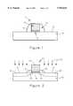
- FIG. 1is a cross sectional view of part of a silicon wafer and the first phase of a MOSFET on the silicon chip.
- FIG. 2is a cross sectional view of part of a silicon wafer with the MOSFET undergoing,/amorphization.
- FIG. 3is a cross sectional view of part of a silicon wafer with the MOSFET undergoing dopant implantation.
- FIG. 4is a cross sectional view of part of a silicon wafer with the MOSFET undergoing laser annealing.
- FIG. 1is a cross sectional view of part of a silicon wafer 10 and the first phase of a MOSFET 11 on the silicon wafer 10.
- the surface of the silicon wafer 10forms a substrate 12 for the MOSFET 11.
- the first phase of the MOSFET 11has a gate 17 placed on a gate oxide 19 placed on the surface of the substrate 12.
- Plasma-enhanced chemical vapor deposition (PECVD)is used to deposit oxide spacers.
- a plasma dry etcheris used to etch back the oxide to form the oxide spacers 15 adjacent to the gate 17 as shown in FIG. 1.
- the manufacture of the first phase of the MOSFETis according to conventional means.
- a well-controlled wet chemical etching(such as spray etching) is used to further etch the oxide spacers 15 so that only a known thickness of the oxide film is left at the corner of the gate 17, gate oxide 19 and substrate 12, as shown in FIG. 2.
- a first ion beam 21provides a stream of either Si + or Ge + or Xe + ions, which creates shallow amorphous silicon regions 23 under the etched oxide spacers 15 and deep amorphous silicon regions 25 away from the etched oxide spacers 15.
- the oxide spacers 15are thin enough to allow some of the ions from the first ion beam 21 pass through to the substrate 12, but are thick enough to absorb some of the energy from the ions in the first ion beam 21.
- the ions passing through the oxide spacersare slowed, so that they create the shallow amorphous regions 23 below the spacers 15. Ions that do not pass into the oxide spacers 15 and the gate oxide 19 are not slowed down or stopped and therefore create the deep amorphous regions 25.
- the oxide spacer 15is then etched away, using anisotropic plasma etching.
- a second ion beam 27is used to implant a high dose dopant into the shallow and deep amorphous silicon regions 23, 25, as shown in FIG. 3.
- arsenic or phosphorousis used as the dopant.
- boron or boron trifluorideis used as the dopant.
- Plasma-enhanced chemical vapor depositionis used to deposit an oxide film barrier layer 29 over the surface of the silicon wafer 10 and the gate oxide 19, as shown in FIG. 4.
- An excimer laser beam 33is used to provide ultra-rapid annealing.
- the deep and shallow amorphous silicon regions 23, 25are melted by the laser annealing causing the dopant to diffuse throughout the deep and shallow amorphous silicon regions 23, 25.
- the deep amorphous regions 25become source/drain regions 35.
- the shallow amorphous regions 23become source/drain extensions 37.
- the laser annealingcauses complete activation of the dopant causing high conductivity in both the source/drain regions 35 and the source/drain extensions 37.
- the metal layer 31 and the oxide film barrier layer 29are removed, and the conventional MOSFET processing is done to form a transistor, including the silicidation of the source/drain junctions. Because the source/drain junctions are deep, they can be more easily silicidated.
- the terms deep amorphous regions and shallow amorphous regionsare relative terms, mainly meaning that the deep amorphous regions are significantly deeper than the shallow amorphous regions due to the use of the spacers to slow ions from the ion beam for amorphization.
- the deep amorphous regionsare more than twice as deep as the shallow amorphous regions. More preferably, the deep amorphous regions are between 3 to 4 times as deep as the shallow amorphous regions.
- An example of depths in the preferred embodiment, shallow amorphous regionsmay be from 20-40 nm in depth and deep amorphous regions may be from 60-160 nm in depth.
Landscapes
- Physics & Mathematics (AREA)
- Engineering & Computer Science (AREA)
- High Energy & Nuclear Physics (AREA)
- General Physics & Mathematics (AREA)
- Toxicology (AREA)
- Condensed Matter Physics & Semiconductors (AREA)
- Health & Medical Sciences (AREA)
- Manufacturing & Machinery (AREA)
- Computer Hardware Design (AREA)
- Microelectronics & Electronic Packaging (AREA)
- Power Engineering (AREA)
- Electromagnetism (AREA)
- Optics & Photonics (AREA)
- Insulated Gate Type Field-Effect Transistor (AREA)
Abstract
Description
Claims (12)
Priority Applications (1)
| Application Number | Priority Date | Filing Date | Title |
|---|---|---|---|
| US09/238,359US5953615A (en) | 1999-01-27 | 1999-01-27 | Pre-amorphization process for source/drain junction |
Applications Claiming Priority (1)
| Application Number | Priority Date | Filing Date | Title |
|---|---|---|---|
| US09/238,359US5953615A (en) | 1999-01-27 | 1999-01-27 | Pre-amorphization process for source/drain junction |
Publications (1)
| Publication Number | Publication Date |
|---|---|
| US5953615Atrue US5953615A (en) | 1999-09-14 |
Family
ID=22897527
Family Applications (1)
| Application Number | Title | Priority Date | Filing Date |
|---|---|---|---|
| US09/238,359Expired - LifetimeUS5953615A (en) | 1999-01-27 | 1999-01-27 | Pre-amorphization process for source/drain junction |
Country Status (1)
| Country | Link |
|---|---|
| US (1) | US5953615A (en) |
Cited By (37)
| Publication number | Priority date | Publication date | Assignee | Title |
|---|---|---|---|---|
| US6074937A (en)* | 1997-12-18 | 2000-06-13 | Advanced Micro Devices, Inc. | End-of-range damage suppression for ultra-shallow junction formation |
| US6114206A (en)* | 1998-11-06 | 2000-09-05 | Advanced Micro Devices, Inc. | Multiple threshold voltage transistor implemented by a damascene process |
| US6194279B1 (en)* | 1999-06-28 | 2001-02-27 | United Silicon Incorporated | Fabrication method for gate spacer |
| US6225176B1 (en)* | 1999-02-22 | 2001-05-01 | Advanced Micro Devices, Inc. | Step drain and source junction formation |
| US6262456B1 (en) | 1998-11-06 | 2001-07-17 | Advanced Micro Devices, Inc. | Integrated circuit having transistors with different threshold voltages |
| US6284672B1 (en)* | 1999-03-02 | 2001-09-04 | Advanced Micro Devices, Inc. | Method of forming a super-shallow amorphous layer in silicon |
| US6335253B1 (en) | 2000-07-12 | 2002-01-01 | Chartered Semiconductor Manufacturing Ltd. | Method to form MOS transistors with shallow junctions using laser annealing |
| US6365446B1 (en) | 2000-07-03 | 2002-04-02 | Chartered Semiconductor Manufacturing Ltd. | Formation of silicided ultra-shallow junctions using implant through metal technology and laser annealing process |
| US6372584B1 (en)* | 2000-08-01 | 2002-04-16 | Advanced Micro Devices, Inc. | Method for making raised source/drain regions using laser |
| US6426278B1 (en)* | 1999-10-07 | 2002-07-30 | International Business Machines Corporation | Projection gas immersion laser dopant process (PGILD) fabrication of diffusion halos |
| WO2002101811A1 (en)* | 2001-06-11 | 2002-12-19 | Advanced Micro Devices, Inc. | Soi mosfet with hyperabrupt source and drain junctions |
| WO2003012844A1 (en)* | 2001-08-01 | 2003-02-13 | Advanced Micro Devices, Inc. | Xe preamorphizing implantation |
| US6521502B1 (en) | 2000-08-07 | 2003-02-18 | Advanced Micro Devices, Inc. | Solid phase epitaxy activation process for source/drain junction extensions and halo regions |
| US6555439B1 (en)* | 2001-12-18 | 2003-04-29 | Advanced Micro Devices, Inc. | Partial recrystallization of source/drain region before laser thermal annealing |
| US6630386B1 (en) | 2000-07-18 | 2003-10-07 | Advanced Micro Devices, Inc | CMOS manufacturing process with self-amorphized source/drain junctions and extensions |
| US6630385B1 (en)* | 2001-04-27 | 2003-10-07 | Advanced Micro Devices, Inc. | MOSFET with differential halo implant and annealing strategy |
| WO2003046967A3 (en)* | 2001-11-30 | 2003-10-16 | Koninkl Philips Electronics Nv | Method of forming a doped region in a semiconductor body comprising a step of amorphization by irradiation |
| US6649460B2 (en) | 2001-10-25 | 2003-11-18 | International Business Machines Corporation | Fabricating a substantially self-aligned MOSFET |
| US6689671B1 (en) | 2002-05-22 | 2004-02-10 | Advanced Micro Devices, Inc. | Low temperature solid-phase epitaxy fabrication process for MOS devices built on strained semiconductor substrate |
| US20040087121A1 (en)* | 2002-10-30 | 2004-05-06 | Thorsten Kammler | Method of forming a nickel silicide region in a doped silicon-containing semiconductor area |
| WO2004042809A1 (en)* | 2002-10-30 | 2004-05-21 | Advanced Micro Devices, Inc. | Method of forming a nickel silicide region in a doped silicon-containing semiconductor area |
| US6897118B1 (en)* | 2004-02-11 | 2005-05-24 | Chartered Semiconductor Manufacturing Ltd. | Method of multiple pulse laser annealing to activate ultra-shallow junctions |
| US20050142783A1 (en)* | 2003-12-31 | 2005-06-30 | Kim In S. | Methods of fabricating gate spacers for semiconductor devices |
| US20050142865A1 (en)* | 2003-12-31 | 2005-06-30 | Dongbuanam Semiconductor Inc. | Methods of fabricating via hole and trench |
| US20060205134A1 (en)* | 2005-03-10 | 2006-09-14 | Oki Electric Industry Co., Ltd. | Method for manufacturing a semiconductor device and method for regulating speed of forming an insulating film |
| US20070001243A1 (en)* | 2000-02-29 | 2007-01-04 | Agere Systems, Inc. | Selective laser annealing of semiconductor material |
| US7211489B1 (en) | 2004-09-07 | 2007-05-01 | Advanced Micro Devices, Inc. | Localized halo implant region formed using tilt pre-amorphization implant and laser thermal anneal |
| EP1780776A1 (en)* | 2005-10-28 | 2007-05-02 | STMicroelectronics S.r.l. | Process for manufacturing a high-scale-integration mos device |
| CN1315179C (en)* | 2003-06-17 | 2007-05-09 | 株式会社东芝 | Manufacturing method of semiconductor device |
| US7256122B2 (en) | 2003-12-30 | 2007-08-14 | Dongbu Electronics Co., Ltd. | Method of fabricating semiconductor device |
| WO2009031076A3 (en)* | 2007-09-05 | 2009-05-28 | Nxp Bv | A transistor and a method of manufacturing the same |
| US20100154835A1 (en)* | 2006-04-26 | 2010-06-24 | Advanced Technology Materials, Inc. | Cleaning of semiconductor processing systems |
| US20100176426A1 (en)* | 2007-09-05 | 2010-07-15 | Nxp B.V. | Transistor and method of manufacturing the same |
| US20100261298A1 (en)* | 2009-04-09 | 2010-10-14 | Texas Instruments Incorporated | Curvature reduction for semiconductor wafers |
| US8216945B2 (en) | 2009-04-09 | 2012-07-10 | Texas Instruments Incorporated | Wafer planarity control between pattern levels |
| US20130023104A1 (en)* | 2011-07-19 | 2013-01-24 | Tatsunori Isogai | Method for manufacturing semiconductor device |
| US12168147B2 (en) | 2019-03-08 | 2024-12-17 | Mevion Medical Systems, Inc. | Collimator and energy degrader for a particle therapy system |
Citations (3)
| Publication number | Priority date | Publication date | Assignee | Title |
|---|---|---|---|---|
| US4584026A (en)* | 1984-07-25 | 1986-04-22 | Rca Corporation | Ion-implantation of phosphorus, arsenic or boron by pre-amorphizing with fluorine ions |
| JPH04158528A (en)* | 1990-10-22 | 1992-06-01 | Seiko Epson Corp | Manufacturing method of semiconductor device |
| US5266510A (en)* | 1990-08-09 | 1993-11-30 | Micron Technology, Inc. | High performance sub-micron p-channel transistor with germanium implant |
- 1999
- 1999-01-27USUS09/238,359patent/US5953615A/ennot_activeExpired - Lifetime
Patent Citations (3)
| Publication number | Priority date | Publication date | Assignee | Title |
|---|---|---|---|---|
| US4584026A (en)* | 1984-07-25 | 1986-04-22 | Rca Corporation | Ion-implantation of phosphorus, arsenic or boron by pre-amorphizing with fluorine ions |
| US5266510A (en)* | 1990-08-09 | 1993-11-30 | Micron Technology, Inc. | High performance sub-micron p-channel transistor with germanium implant |
| JPH04158528A (en)* | 1990-10-22 | 1992-06-01 | Seiko Epson Corp | Manufacturing method of semiconductor device |
Cited By (51)
| Publication number | Priority date | Publication date | Assignee | Title |
|---|---|---|---|---|
| US6074937A (en)* | 1997-12-18 | 2000-06-13 | Advanced Micro Devices, Inc. | End-of-range damage suppression for ultra-shallow junction formation |
| US6114206A (en)* | 1998-11-06 | 2000-09-05 | Advanced Micro Devices, Inc. | Multiple threshold voltage transistor implemented by a damascene process |
| US6262456B1 (en) | 1998-11-06 | 2001-07-17 | Advanced Micro Devices, Inc. | Integrated circuit having transistors with different threshold voltages |
| US6225176B1 (en)* | 1999-02-22 | 2001-05-01 | Advanced Micro Devices, Inc. | Step drain and source junction formation |
| US6284672B1 (en)* | 1999-03-02 | 2001-09-04 | Advanced Micro Devices, Inc. | Method of forming a super-shallow amorphous layer in silicon |
| US6194279B1 (en)* | 1999-06-28 | 2001-02-27 | United Silicon Incorporated | Fabrication method for gate spacer |
| US6426278B1 (en)* | 1999-10-07 | 2002-07-30 | International Business Machines Corporation | Projection gas immersion laser dopant process (PGILD) fabrication of diffusion halos |
| US20070001243A1 (en)* | 2000-02-29 | 2007-01-04 | Agere Systems, Inc. | Selective laser annealing of semiconductor material |
| US7605064B2 (en) | 2000-02-29 | 2009-10-20 | Agere Systems Inc. | Selective laser annealing of semiconductor material |
| US6624489B2 (en) | 2000-07-03 | 2003-09-23 | Chartered Semiconductor Manufacturing Ltd. | Formation of silicided shallow junctions using implant through metal technology and laser annealing process |
| US6365446B1 (en) | 2000-07-03 | 2002-04-02 | Chartered Semiconductor Manufacturing Ltd. | Formation of silicided ultra-shallow junctions using implant through metal technology and laser annealing process |
| US6335253B1 (en) | 2000-07-12 | 2002-01-01 | Chartered Semiconductor Manufacturing Ltd. | Method to form MOS transistors with shallow junctions using laser annealing |
| US6630386B1 (en) | 2000-07-18 | 2003-10-07 | Advanced Micro Devices, Inc | CMOS manufacturing process with self-amorphized source/drain junctions and extensions |
| US6372584B1 (en)* | 2000-08-01 | 2002-04-16 | Advanced Micro Devices, Inc. | Method for making raised source/drain regions using laser |
| US6521502B1 (en) | 2000-08-07 | 2003-02-18 | Advanced Micro Devices, Inc. | Solid phase epitaxy activation process for source/drain junction extensions and halo regions |
| US6630385B1 (en)* | 2001-04-27 | 2003-10-07 | Advanced Micro Devices, Inc. | MOSFET with differential halo implant and annealing strategy |
| WO2002101811A1 (en)* | 2001-06-11 | 2002-12-19 | Advanced Micro Devices, Inc. | Soi mosfet with hyperabrupt source and drain junctions |
| WO2003012844A1 (en)* | 2001-08-01 | 2003-02-13 | Advanced Micro Devices, Inc. | Xe preamorphizing implantation |
| CN1307688C (en)* | 2001-08-01 | 2007-03-28 | 先进微装置公司 | xenon pre-amorphization implantation method |
| US6624037B2 (en) | 2001-08-01 | 2003-09-23 | Advanced Micro Devices, Inc. | XE preamorphizing implantation |
| EP1511071A3 (en)* | 2001-08-01 | 2009-01-14 | Advanced Micro Devices, Inc. | Xe preamorphising implantation |
| KR100880687B1 (en)* | 2001-08-01 | 2009-01-30 | 어드밴스드 마이크로 디바이시즈, 인코포레이티드 | XE pre-crystallization injection |
| US6649460B2 (en) | 2001-10-25 | 2003-11-18 | International Business Machines Corporation | Fabricating a substantially self-aligned MOSFET |
| US20050003638A1 (en)* | 2001-11-30 | 2005-01-06 | Stolk Peter Adriaan | Method of manufacturing a semiconductor device |
| US6982212B2 (en) | 2001-11-30 | 2006-01-03 | Koninklijke Philips Electronics N.V. | Method of manufacturing a semiconductor device |
| WO2003046967A3 (en)* | 2001-11-30 | 2003-10-16 | Koninkl Philips Electronics Nv | Method of forming a doped region in a semiconductor body comprising a step of amorphization by irradiation |
| US6555439B1 (en)* | 2001-12-18 | 2003-04-29 | Advanced Micro Devices, Inc. | Partial recrystallization of source/drain region before laser thermal annealing |
| US6689671B1 (en) | 2002-05-22 | 2004-02-10 | Advanced Micro Devices, Inc. | Low temperature solid-phase epitaxy fabrication process for MOS devices built on strained semiconductor substrate |
| WO2004042809A1 (en)* | 2002-10-30 | 2004-05-21 | Advanced Micro Devices, Inc. | Method of forming a nickel silicide region in a doped silicon-containing semiconductor area |
| US20040087121A1 (en)* | 2002-10-30 | 2004-05-06 | Thorsten Kammler | Method of forming a nickel silicide region in a doped silicon-containing semiconductor area |
| CN1315179C (en)* | 2003-06-17 | 2007-05-09 | 株式会社东芝 | Manufacturing method of semiconductor device |
| US7256122B2 (en) | 2003-12-30 | 2007-08-14 | Dongbu Electronics Co., Ltd. | Method of fabricating semiconductor device |
| US20050142783A1 (en)* | 2003-12-31 | 2005-06-30 | Kim In S. | Methods of fabricating gate spacers for semiconductor devices |
| US7259105B2 (en) | 2003-12-31 | 2007-08-21 | Dongbu Electronics Co., Ltd. | Methods of fabricating gate spacers for semiconductor devices |
| US7297630B2 (en) | 2003-12-31 | 2007-11-20 | Dongbu Electronics Co., Ltd. | Methods of fabricating via hole and trench |
| US20050142865A1 (en)* | 2003-12-31 | 2005-06-30 | Dongbuanam Semiconductor Inc. | Methods of fabricating via hole and trench |
| US6897118B1 (en)* | 2004-02-11 | 2005-05-24 | Chartered Semiconductor Manufacturing Ltd. | Method of multiple pulse laser annealing to activate ultra-shallow junctions |
| US7211489B1 (en) | 2004-09-07 | 2007-05-01 | Advanced Micro Devices, Inc. | Localized halo implant region formed using tilt pre-amorphization implant and laser thermal anneal |
| US20060205134A1 (en)* | 2005-03-10 | 2006-09-14 | Oki Electric Industry Co., Ltd. | Method for manufacturing a semiconductor device and method for regulating speed of forming an insulating film |
| EP1780776A1 (en)* | 2005-10-28 | 2007-05-02 | STMicroelectronics S.r.l. | Process for manufacturing a high-scale-integration mos device |
| US20100154835A1 (en)* | 2006-04-26 | 2010-06-24 | Advanced Technology Materials, Inc. | Cleaning of semiconductor processing systems |
| US8603252B2 (en)* | 2006-04-26 | 2013-12-10 | Advanced Technology Materials, Inc. | Cleaning of semiconductor processing systems |
| WO2009031076A3 (en)* | 2007-09-05 | 2009-05-28 | Nxp Bv | A transistor and a method of manufacturing the same |
| US20100176426A1 (en)* | 2007-09-05 | 2010-07-15 | Nxp B.V. | Transistor and method of manufacturing the same |
| US20100200897A1 (en)* | 2007-09-05 | 2010-08-12 | Nxp B.V. | Transistor and method of manufacturing the same |
| US8202782B2 (en) | 2007-09-05 | 2012-06-19 | Nxp B.V. | Method of manufacturing transistor |
| US20100261298A1 (en)* | 2009-04-09 | 2010-10-14 | Texas Instruments Incorporated | Curvature reduction for semiconductor wafers |
| US8216945B2 (en) | 2009-04-09 | 2012-07-10 | Texas Instruments Incorporated | Wafer planarity control between pattern levels |
| US8252609B2 (en) | 2009-04-09 | 2012-08-28 | Texas Instruments Incorporated | Curvature reduction for semiconductor wafers |
| US20130023104A1 (en)* | 2011-07-19 | 2013-01-24 | Tatsunori Isogai | Method for manufacturing semiconductor device |
| US12168147B2 (en) | 2019-03-08 | 2024-12-17 | Mevion Medical Systems, Inc. | Collimator and energy degrader for a particle therapy system |
Similar Documents
| Publication | Publication Date | Title |
|---|---|---|
| US5953615A (en) | Pre-amorphization process for source/drain junction | |
| US6391731B1 (en) | Activating source and drain junctions and extensions using a single laser anneal | |
| US8187959B2 (en) | Semiconductor substrate with solid phase epitaxial regrowth with reduced junction leakage and method of producing same | |
| US6335253B1 (en) | Method to form MOS transistors with shallow junctions using laser annealing | |
| US7358167B2 (en) | Implantation process in semiconductor fabrication | |
| JP2002524846A (en) | Gas immersion laser annealing method suitable for applications in the fabrication of small integrated circuits | |
| US20100255666A1 (en) | Thermal processing method | |
| US6355543B1 (en) | Laser annealing for forming shallow source/drain extension for MOS transistor | |
| US6475885B1 (en) | Source/drain formation with sub-amorphizing implantation | |
| JP2003188373A (en) | Semiconductor device and method of manufacturing the same | |
| US5677213A (en) | Method for forming a semiconductor device having a shallow junction and a low sheet resistance | |
| US5698461A (en) | Method for fabricating lightly doped drain metal oxide semiconductor field effect transistor | |
| US20010031522A1 (en) | Method of manufacturing a semiconductor device | |
| US7041583B2 (en) | Method of removing features using an improved removal process in the fabrication of a semiconductor device | |
| TW445524B (en) | Method for forming raised source and drain | |
| US6194293B1 (en) | Channel formation after source and drain regions are formed | |
| US6933188B1 (en) | Use of a selective hard mask for the integration of double diffused drain MOS devices in deep sub-micron fabrication technologies | |
| WO2006041837A1 (en) | Pre-silicidation amorphization in semiconductor device nickel sili cide | |
| JP5103695B2 (en) | Method for manufacturing field-effect semiconductor device | |
| EP1697977B1 (en) | Method of manufacturing a semiconductor device | |
| US20240203735A1 (en) | Method for producing doped transistor source and drain | |
| CN1303657C (en) | Method for manufacturing pMOS for titanium silicide preparing process window | |
| JP3893997B2 (en) | Manufacturing method of semiconductor device | |
| JP3528892B2 (en) | Method for manufacturing semiconductor device | |
| US20040142519A1 (en) | Methods of manufacturing a semiconductor device |
Legal Events
| Date | Code | Title | Description |
|---|---|---|---|
| AS | Assignment | Owner name:ADVANCED MICRO DEVICES, CALIFORNIA Free format text:ASSIGNMENT OF ASSIGNORS INTEREST;ASSIGNOR:YU, BIN;REEL/FRAME:009739/0150 Effective date:19990115 | |
| STCF | Information on status: patent grant | Free format text:PATENTED CASE | |
| CC | Certificate of correction | ||
| FPAY | Fee payment | Year of fee payment:4 | |
| FPAY | Fee payment | Year of fee payment:8 | |
| AS | Assignment | Owner name:GLOBALFOUNDRIES INC., CAYMAN ISLANDS Free format text:AFFIRMATION OF PATENT ASSIGNMENT;ASSIGNOR:ADVANCED MICRO DEVICES, INC.;REEL/FRAME:023119/0083 Effective date:20090630 | |
| FPAY | Fee payment | Year of fee payment:12 | |
| AS | Assignment | Owner name:WILMINGTON TRUST, NATIONAL ASSOCIATION, DELAWARE Free format text:SECURITY AGREEMENT;ASSIGNOR:GLOBALFOUNDRIES INC.;REEL/FRAME:049490/0001 Effective date:20181127 | |
| AS | Assignment | Owner name:GLOBALFOUNDRIES INC., CAYMAN ISLANDS Free format text:RELEASE BY SECURED PARTY;ASSIGNOR:WILMINGTON TRUST, NATIONAL ASSOCIATION;REEL/FRAME:054636/0001 Effective date:20201117 | |
| AS | Assignment | Owner name:GLOBALFOUNDRIES U.S. INC., NEW YORK Free format text:RELEASE BY SECURED PARTY;ASSIGNOR:WILMINGTON TRUST, NATIONAL ASSOCIATION;REEL/FRAME:056987/0001 Effective date:20201117 |