US5952833A - Programmable voltage divider and method for testing the impedance of a programmable element - Google Patents
Programmable voltage divider and method for testing the impedance of a programmable elementDownload PDFInfo
- Publication number
- US5952833A US5952833AUS08/813,063US81306397AUS5952833AUS 5952833 AUS5952833 AUS 5952833AUS 81306397 AUS81306397 AUS 81306397AUS 5952833 AUS5952833 AUS 5952833A
- Authority
- US
- United States
- Prior art keywords
- node
- coupled
- divider
- circuit
- switch
- Prior art date
- Legal status (The legal status is an assumption and is not a legal conclusion. Google has not performed a legal analysis and makes no representation as to the accuracy of the status listed.)
- Expired - Lifetime
Links
Images


Classifications
- G—PHYSICS
- G01—MEASURING; TESTING
- G01R—MEASURING ELECTRIC VARIABLES; MEASURING MAGNETIC VARIABLES
- G01R31/00—Arrangements for testing electric properties; Arrangements for locating electric faults; Arrangements for electrical testing characterised by what is being tested not provided for elsewhere
- G01R31/28—Testing of electronic circuits, e.g. by signal tracer
- G01R31/2832—Specific tests of electronic circuits not provided for elsewhere
- G01R31/2836—Fault-finding or characterising
- G01R31/2843—In-circuit-testing
- G—PHYSICS
- G01—MEASURING; TESTING
- G01R—MEASURING ELECTRIC VARIABLES; MEASURING MAGNETIC VARIABLES
- G01R15/00—Details of measuring arrangements of the types provided for in groups G01R17/00 - G01R29/00, G01R33/00 - G01R33/26 or G01R35/00
- G01R15/08—Circuits for altering the measuring range
- G01R15/09—Autoranging circuits
- G—PHYSICS
- G06—COMPUTING OR CALCULATING; COUNTING
- G06Q—INFORMATION AND COMMUNICATION TECHNOLOGY [ICT] SPECIALLY ADAPTED FOR ADMINISTRATIVE, COMMERCIAL, FINANCIAL, MANAGERIAL OR SUPERVISORY PURPOSES; SYSTEMS OR METHODS SPECIALLY ADAPTED FOR ADMINISTRATIVE, COMMERCIAL, FINANCIAL, MANAGERIAL OR SUPERVISORY PURPOSES, NOT OTHERWISE PROVIDED FOR
- G06Q20/00—Payment architectures, schemes or protocols
- G06Q20/08—Payment architectures
- G06Q20/20—Point-of-sale [POS] network systems
- G06Q20/202—Interconnection or interaction of plural electronic cash registers [ECR] or to host computer, e.g. network details, transfer of information from host to ECR or from ECR to ECR
- G—PHYSICS
- G11—INFORMATION STORAGE
- G11C—STATIC STORES
- G11C5/00—Details of stores covered by group G11C11/00
- G11C5/14—Power supply arrangements, e.g. power down, chip selection or deselection, layout of wirings or power grids, or multiple supply levels
- G11C5/147—Voltage reference generators, voltage or current regulators; Internally lowered supply levels; Compensation for voltage drops
Definitions
- the present inventionrelates generally to electronic circuits, and more specifically to a programmable circuit that allows one to test the impedance of a programmable element, such as a fuse, during a test mode, and to a method for performing such a test.
- a programmable elementsuch as a fuse
- circuitsare programmable to operate in one or more particular modes, or to have one or more particular circuit configurations.
- An example of the latter type of circuitis a memory that includes redundant memory columns for replacing defective array memory columns.
- a circuit testerWhen a circuit tester discovers a defective array column, it programs the memory such that when an external device addresses the defective column, data is routed to a selected redundant column in a manner that is transparent to the external device.
- the manufacturerprograms such integrated circuits at the factory before shipping them to customers.
- These integrated circuitseach typically include a bank of nonvolatile, programmable memory elements that the manufacturer programs to set a circuit in the desired operational mode or circuit configuration. Examples of such elements include electrically erasable and programmable read-only memory (EEPROM) cells, fuses, and antifuses.
- EEPROMelectrically erasable and programmable read-only memory
- An integrated circuitoften incorporates into its programmable bank the type of programmable element that is the most similar to other elements or components of the circuit.
- a Flash-EEPROM deviceoften includes a bank of EEPROM cells, but a dynamic random access memory (DRAM) often includes a bank of antifuses, which are similar in structure to the DRAM storage capacitors.
- DRAMdynamic random access memory
- such a programmable elementtypically has a first impedance in an unprogrammed state, and a second, different impedance in a programmed state.
- an antifusehas a high impedance in an unprogrammed state, and thus is essentially an open circuit, and has a low impedance in a programmed state, and thus is essentially a short circuit.
- a fuseis essentially a short circuit in an unprogrammed state, and is essentially an open circuit in a programmed state.
- the manufactureroften measures the impedances of the programmed elements in an analog fashion after it finishes programming the entire programmable bank.
- the analog testerperforms these measurements sequentially by placing a voltage across each programmed element and measuring the current therethrough. If the manufacture discovers a programmed element that does not have the desired impedance, it can reprogram the element one or more times until it has the desired impedance.
- a problem with this analog testing techniqueis that it often takes too long for high-density integrated circuits. As the number of circuit components in an integrated circuit increases, so does the number of operational modes and circuit configurations that the circuit supports. Therefore, the number of programmable elements in the programmable bank also increases to accommodate the additional operational modes and circuit configurations. For example, a 4 megabit DRAM may have 20 antifuses in its programmable bank, but a 64 megabit DRAM may have 640 antifuses. Furthermore, measuring the impedance in an analog fashion is relatively slow because of the parasitic capacitances associated with the test path and each programmed element. Thus, increasing the storage capacity of a DRAM by a factor of 16 can potentially increase the number of antifuses, and thus the already lengthy testing time, by a factor of 32. Additionally, testers that can perform analog measurements are often expensive and complicated to operate in the analog-testing mode.
- a programmable voltage dividerhas normal and test modes of operation.
- the dividerincludes first and second supply nodes, a divider node that provides a data value, and a first divider element that is coupled between the first supply node and the divider node.
- the divideralso includes a controlled node, a second divider element that has a selectable resistivity and that is coupled between the divider node and the controlled node, and a test circuit that is coupled between the controlled node and the second supply node.
- the test circuitgenerates a voltage at the controlled node during the normal mode of operation, and varies this voltage during the test mode of operation.
- the test circuitincludes a first switch coupled between the controlled node and the second supply node and a series combination of a second switch and a voltage source, the series combination coupled in parallel with the first switch. During the test mode, the test circuit opens the first switch and closes the second switch.
- the test circuitincludes a first switch coupled between the controlled node and the second supply node, and a series combination of a second switch and an impedance element, the series combination coupled in parallel with the first switch. During the test mode, the test circuit opens the first switch and closes the second switch.
- the test circuitincludes a first switch coupled between the controlled node and the second supply node, and a diode coupled in parallel with the first switch. During the test mode, the test circuit opens the first switch.
- An advantage of the present inventionis that it allows faster testing of programmable elements as compared with the prior art. Another advantage is that the present invention allows digital testing of programmable elements instead of analog testing.
- FIG. 1is a schematic diagram of a programmable bank according to a first embodiment of the invention.
- FIG. 2is a schematic diagram of a programmable bank according to a second embodiment of the invention.
- FIG. 3is a schematic diagram of a first alternative embodiment of the test circuit of FIG. 2.
- FIG. 4is a schematic diagram of a second alternative embodiment of the test circuit of FIG. 2.
- FIG. 5is a schematic diagram of a programmable bank according to a third embodiment of the invention.
- FIG. 6is a schematic diagram of an alternative embodiment of the programmable elements of FIGS. 1, 2 and 5.
- FIG. 7is a schematic diagram of a programmable bank according to a fourth embodiment of the invention.
- FIG. 8is a schematic block diagram of a memory device that incorporates a programmable bank according to the present invention.
- FIG. 9is a schematic block diagram of a computer system that incorporates the memory device of FIG. 8.
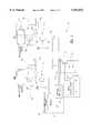
- FIG. 1is a schematic diagram of a programmable bank 10 according to a first embodiment of the invention.
- the bank 10includes individually programmable circuits 12 0 -12 n , which generate binary reference signals P 0 -P n at respective output nodes 14 0 -14 n .
- the actual logic levels of the signals P 0 -P ndepend upon the states in which the circuits 12 0 -12 n are programmed.
- the integrated circuit(not shown in FIG. 1) that incorporates the bank 10 uses the signals P 0 -P n to select its operational modes or to configure its circuitry.
- the bank 10also includes a test circuit 16, which allows the manufacturer to test the programmable circuits 12 0 -12 n in a digital manner, i.e., by merely reading the values P 0 -P n .
- the manufacturercan test the bank 10 in a manner that is both faster and easier than prior testing techniques.
- the bank 10may support conventional analog testing as well as the inventive digital testing. The bank 10 is discussed below in greater detail with specific reference to the programmable circuit 12 0 , which is similar in structure and operation to the other programmable circuits 12 1 -12 n .
- the programmable circuit 12 0includes a programmable element 18 0 , which is an antifuse in this first embodiment of the invention.
- a first node of the antifuse 18 0is coupled to a test node 20, which is common to the first nodes of all the antifuses 18 0 -18 n .
- a second nodeis coupled to an isolation device 19 0 , which limits the voltage across the antifuse 18 0 during normal operation of the bank 10.
- the device 19is an NMOS transistor, which has its gate coupled to a voltage V 1 during normal operation of the bank 10, and to 0 V, i.e., ground, during programming of the bank 10.
- the circuit 12 0also includes a latch/pull-up circuit 22 0 , which generates the signal P 0 in response to the state of the antifuse 18 0 .
- the circuit 22 0includes an inverter 24 0 , which has an input terminal coupled to a reference node 25 0 .
- the circuit 22 0also includes a feedback switch 26 0 , which together with the inverter 24 0 forms a latch 27 0 , an impedance element, e.g., a pull-up or divider device 28 0 , and an initialization switch 30 0 , which allows the circuit 22 0 to generate the desired value for P 0 during the initial power-up of the integrated circuit that incorporates the bank 10.
- the feedback switch 26 0 and the initialization switch 30 0are PMOS transistors, and the pull-up device 28 0 is a controlled-current, i.e., long-channel, PMOS transistor.
- An advantage of the circuit 22 0is that after the initialization pulse is removed, the circuit 12 0 draws no quiescent supply current regardless of whether the antifuse 18 0 is programmed or unprogrammed.
- the programmable bank 10also includes programming/analog-testing circuitry 32, which is coupled across each of the antifuses 18 0 -18 n .
- the programming circuitry 32includes a program/test circuit 34, which provides a programming voltage at the common node 20 to program selected ones of the antifuses 18 0 -18 n .
- a tester(not shown in FIG. 1) can be coupled to the common node 20 to provide a test voltage and measure the resultant test current to determine the impedances of the antifuses 18 0 -18 n in an analog fashion.
- a program/decoder 36couples to ground the first node of an antifuse 18 that is selected for either programming or analog testing.
- the bank 10further includes a bank-mode circuit 37, which includes the test circuit 16, a normal-mode switch 38, and a conventional mode-control circuit 44.
- the switch 38couples the common node 20 to ground during normal operation of the bank 10.
- the test circuit 16includes a switch 40 that couples the test node to ground through an impedance element 42 in a test mode during digital testing of the bank 10.
- the mode-control circuit 44controls the switch 38 and the switch 40 of the test circuit 16.
- the switches 38 and 40are NMOS transistors
- the impedance element 42is a resistor.
- the impedance element 42can be a long-channel PMOS transistor or any other conventional impedance device.
- the gate of the isolation transistor 19 0is coupled to ground such that the transistor 19 0 is inactive, and thus electrically isolates the antifuse 18 0 from the latch/pull-up circuit 22 0 .
- the decoder 36couples the first node of the antifuse 18 0 to ground.
- the program/test circuit 34then provides on the common node 20 a programming voltage that programs or "blows" the antifuse 18 0 , i.e., significantly lowers the impedance between its first and second nodes. In one aspect of the invention, the programming voltage is between 7 V and 9 V. Once programmed, the antifuse 18 0 should be essentially a short circuit.
- the program/test circuit 34provides a test voltage on the common node 20, and a conventional tester (not shown in FIG. 1) measures the current through the antifuse 18 0 . If the measured impedance is less than a desired maximum impedance, the antifuse 18 0 passes the test and is deemed to have been properly programmed. In one aspect of the invention, the desired maximum impedance is 300 ohms.
- An initialization pulsethen activates the switch 30 0 for a time sufficient to set the latch 27 0 , which generates P 0 equal to logic 1 if the antifuse 18 0 is programmed, or generates P 0 equal to logic 0 if the antifuse 18 0 is unprogrammed.
- a relatively large currentflows through the switch 30 0 , the pull-up device 28 0 , the active isolation transistor 19 0 , and the antifuse 18 0 .
- the programmable circuit 12 0acts as a voltage divider and generates a reference voltage at the reference node 25 0 .
- the antifuse 18 0has a relatively low impedance, which is typically no more that a few hundred ohms, the reference voltage is low enough to represent a logic 0, and thus the inverter 24 0 generates P 0 equal to logic 1.
- the logic 1 at the output 14 0 of the inverter 24 0turns off the feedback switch 26 0 .
- the inactive feedback switch 26 0reinforces the logic 0 at the input of the latch 24 0 so that the signal P 0 remains equal to logic 1.
- the device 28 0pulls up the reference voltage at the node 25 0 to approximately Vcc, which is high enough to represent a logic 1, and the inverter 24 0 generates P 0 equal to logic 0, which turns on the feedback switch 26 0 .
- the active feedback switch 26 0reinforces the logic 1 at the input of the latch 24 0 so that the signal P 0 remains equal to logic 0.
- the isolation transistor 19 0maintains the voltage at the first node of the antifuse 18 0 at one threshold voltage below V 1 , which as stated above is approximately Vcc/2 in one aspect of the invention.
- V 1which as stated above is approximately Vcc/2 in one aspect of the invention.
- the programmed antifuses 18 0 -18 nare tested to make sure that they are properly programmed, i.e., that their resistance is less than a desired maximum value.
- the programmed resistance of the antifuse 18 0is tested.
- the circuit 12 0operates in a manner similar to the normal operating mode described above, except that the mode-control circuit 44 shuts off the switch 38, and turns on the switch 40, thereby coupling the common node 20 to ground through the impedance element 42.
- the impedance element 42effectively increases the impedance of the antifuse 18 0 , i.e., increases the impedance of the lower leg of the voltage divider, and thus increases the reference voltage at the node 25 0 . Therefore, if the circuit 12 0 generates P 0 equal to logic 1 when the impedance element 42 is coupled between the antifuse 18 0 and ground, then the manufacturer can be virtually certain that the circuit 12 0 will generate P 0 equal to logic 1 during normal operation when the active switch 38 couples the antifuse 18 0 directly to ground. Conversely, if during the digital test mode the circuit 12 0 generates P 0 equal to logic 0, then the manufacturer knows that the antifuse 18 0 is improperly programmed, or not programmed at all. At this point, one can instruct the programming circuitry 32 to reprogram the antifuse 18 0 . Or, if the circuit 12 0 is expendable, it can be labeled as defective and not used.
- the impedance element 42has a value of approximately 200 ohms.
- the impedance of the antifuse 18 0is greater than the maximum desired impedance of 300 ohms, the combined impedance between the node 25 0 and ground is greater than or equal to 500 ohms, and P 0 equals logic 0.
- the impedance of the antifuse 18 0is less than the maximum desired impedance, the combined impedance is less than 500 ohms, and P 0 equals logic 1.
- all of the signals P 0 -P nare coupled to a multiplexer (not shown in FIG. 1), which provides a selected one of the signals to an external pin of the device in which the bank 10 is incorporated so that a tester can sequentially read the signals P 0 -P n without internally probing the device.
- the digital test mode according to the first embodiment of the inventionallows a manufacturer to use a tester that need only read digital values instead of measuring an impedance in an analog fashion.
- a tester that reads only digital valuesis often less expensive to purchase and operate than one that must measure analog values.
- such a testeris often easier to operate.
- even a tester that supports both digital and analog testingis often easier and cheaper to operate in the digital mode.
- the digital techniqueis often faster than prior analog techniques. Specifically, in the digital test mode, all the antifuses 18 0 -18 n are connected so that the circuits 12 0 -12 n are operational. Thus, one need only switch a multiplexer or move a probe from one signal P to the next, with no delay other than the multiplexer switching or probe movement time, which are often relatively short. Conversely, in the prior analog testing, each antifuse 18 must be individually switched into the test circuit. Because of the parasitic capacitances and inductances associated with the antifuses 18 and the bank 10 in general, after switching each antifuse 18 into the test circuit, one must wait a relatively long settling time before measuring the current therethrough. Thus, the greater the number of programmed antifuses 18 being tested, the more time the inventive digital technique will save over the prior analog technique.
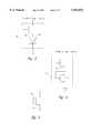
- FIG. 2is a schematic diagram of a programmable bank 46 according to a second embodiment of the invention.
- the bank 46is similar in structure and operation to the bank 10 of FIG. 1, except that in place of the impedance device 42, a test circuit 47 includes a voltage source 48, such as a battery, that generates a positive test voltage VT on the common node 20 during the digital test mode.
- the test voltage VThas the same affect as discussed above for the impedance 42 of FIG. 1 in that it boosts the reference voltage at the node 25 0 , and thus effectively increases the impedance of the antifuse 18 0 during digital testing.
- VTis between 0.7 V and 1.5 V.
- FIG. 3is a schematic diagram of a test circuit 49 according to a first alternative embodiment of the invention.
- the test circuit 49can be used in place of the test circuit 47 of FIG. 2.
- the voltage source 48is a forward-biased PN junction diode 50, which generates a positive test voltage of approximately 0.7 V during the digital test mode when the switch 38 of FIG. 2 is inactive.
- FIG. 4is a schematic diagram of a test circuit 51 according to a second alternative embodiment of the invention.
- the test circuit 51is similar to the test circuit 49 of FIG. 3, except that it includes a diode-connected NMOS transistor 52 instead of a PN junction diode.
- the test circuit 51may include a diode-connected bipolar NPN transistor (not shown in FIG. 4) instead of the NMOS transistor 52.
- FIG. 5is a schematic diagram of a programmable bank 54 according to a third embodiment of the invention.
- the bank 54is similar to the bank 10 of FIG. 1 and the bank 46 of FIG. 2, except that programmable circuits 59 0 include programmable elements 56 0 -56 n , and a test circuit 55 includes a voltage source 58, which generates a negative voltage -VT on the common node 20 during the digital test mode.
- the elements 56 0 -56 nare either laser-cutable fuses or electrically programmable fuses.
- the fuses 56 0 -56 nhave a low impedance when unprogrammed, and have a high impedance when programmed. Because the fuses 56 0 -56 n are not antifuses, the programming circuitry 32 and the isolation transistors 19 of the banks 10 and 46 may be omitted. In this case, the fuses 56 0 -56 n are programmed using conventional means (not shown in FIG. 5) that are external to the device that incorporates the bank 54. Alternatively, if the fuses 56 0 -56 n are electrical fuses, then the bank 54 may include circuitry that is similar to the programming circuitry 32 of FIGS. 1 and 2. But for clarity, FIG. 5 includes no programming circuitry. Because the circuit 59 0 is similar in structure and operation to the circuits 59 1 -59 n , the operation of the bank 54 is discussed below in greater detail with reference to the circuit 59 0 for clarity.
- a technicianuses an ohmmeter (both not shown in FIG. 5) to measure the impedance of the fuse 56 0 .
- the bank 54operates as described above in conjunction with the bank 10 of FIG. 1 and the bank 46 of FIG. 2, except that the circuit 59 0 generates P 0 equal to logic 0 when the fuse 56 0 is programmed, and generates P 0 equal to logic 1 when the fuse 56 0 is unprogrammed. Again, this is because in contrast to the antifuses 18 0 -18 n of FIGS. 1 and 2, the fuses 56 0 -56 n have a high impedance when programmed, and a low impedance when unprogrammed.
- the programmed fuses 56 0 -56 nare tested to make sure that they are properly programmed, i.e., that their programmed resistance is greater than a desired minimum value.
- the circuit 59 0operates like it does during normal mode, except that the mode-control circuit 44 shuts off the switch 38, and turns on the transistor 40 to activate the test circuit 55 and couple the negative test voltage -V T to the common node 20.
- -V Teffectively decreases the impedance of the fuse 56 0 and thus decreases the reference voltage at the node 61 0 as compared with normal operation.
- the manufacturercan be virtually certain that the circuit 59 0 will generate P 0 equal to logic 0 during normal operation when the active switch 38 couples the common node 20 directly to ground. Conversely, if during the digital test mode the circuit 59 0 generates P 0 equal to logic 1, then the manufacturer knows that the fuse 56 0 is improperly programmed, or not programmed at all. At this point, the manufacturer can reprogram the fuse 56 0 , or, if the circuit 59 0 is expendable, can label it as defective and not use it.
- P 0will equal logic 1.
- P 0will equal logic 0.
- all of the signals P 0 -P nmay be coupled to a multiplexer (not shown in FIG. 5), which provides a selected one of the signals to an external pin of the device in which the bank 54 is incorporated so that a tester can sequentially read the signals P 0 -P n .
- FIG. 6is a schematic diagram of nonvolatile programmable element 60 according to an alternative embodiment of the invention.
- the programmable element 60is a EEPROM cell that includes a floating gate 62.
- the EEPROM cell 60In a conventionally defined unprogrammed state, there is no voltage stored on the floating gate 62, and thus the EEPROM cell 60 has a low impedance, i.e., acts as a closed circuit, when a voltage is applied to its gate.
- a negative voltageis stored on the floating gate 62, and thus the EEPROM cell 60 has a high impedance, i.e., acts as an open circuit, when a voltage is applied to its gate.
- the EEPROM cell 60is similar to the fuse elements 56 0 -56 n of FIG. 5, and in one aspect of the invention may be used in place of these fuse elements in the bank 54.
- the EEPROM cell 60resembles the antifuses 18 0 -18 n of FIG. 1.
- EEPROM cells like the cell 60may be used in place of the antifuse elements 18 0 -18 n in the bank 10 of FIG. 1. If, however, one decides to use this unconventional technique, he has to first "unprogram" all of the cells 60 by storing negative voltages on the floating gates 62 thereof.
- FIG. 7is a schematic block diagram of a programmable bank 64 according to a fourth embodiment of the invention.
- the bank 64allows simultaneous digital testing of more than one programmable circuit 66 0 -66 3 at a time. Although the four circuits 66 0 -66 3 are shown here for clarity, the bank 64 may include more or less of these circuits.
- the programmable circuits 66 0 -66 3incorporate antifuses (not shown in FIG. 7), and are thus similar to the circuits 12 0 -12 n of FIGS. 1 and 2.
- the bank 64includes a program/test decoder circuit 68, which selects the circuits 66 0 -66 3 that are to be programmed during a programming mode or are to be tested during a conventional test mode.
- a test circuit 70which is coupled between a node 71 and ground, generates a test voltage or provides a test impedance during a digital test mode.
- the test circuit 70may be similar to the test circuits 16 or 47 of FIGS. 1 and 2.
- a normal-mode switch 78couples the node 71 to ground during normal operation of the bank 64.
- a program/test circuit 72provides a programming voltage during programming of the circuits 66 0 -66 3 , and provides a test voltage during the conventional test mode.
- the circuit 72is a conductive pad to which an external test circuit (not shown in FIG. 7) provides the described programming and test voltages.
- a normal-mode/digital-test-mode switch 74couples a node 76 that is common to the circuits 66 0 -66 3 to the node 71 during normal operation and during the digital test mode.
- a program-mode/conventional-test-mode switch 75couples the common node 76 to the program/test circuit 72 during programming or conventional testing of the bank 64.
- a logic circuit 79receives the output signals P 0 -P 2 of the circuits 66 0 -66 2 , and logically combines them to generate resultant output signals L 0 -L 7 .
- a multiplexer 80provides a selected one of the signals L 0 -L 7 and P 3 to an external terminal of the device incorporating the bank 64 during the digital test mode.
- a mode-control circuit 81controls the operation of the switches 74, 75, and 78, and the test circuit 70.
- the decoder 68receives address signals at its address inputs and couples the selected one of the circuits 66 0 -66 3 to ground through a switching network 69.
- the switch 75is active, and thus couples the common node 76 to the program/test circuit 72.
- the circuit 72generates a program voltage and thus programs those of the circuits 66 0 -66 3 that the decoder 68 selects for programming.
- the circuit 72During the conventional test mode, the circuit 72 generates a test voltage, and external test circuitry measures the current flowing through the circuit 66 under test to determine the resistance of the programmable element therein and whether or not it has a desired value.
- the decoder 68deactivates the switching network 69, the switches 74 and 78 are active, and the switch 75 is inactive.
- the bank 64thus operates similarly to the banks 10 and 46, except that the signals P 0 -P 2 are not considered separately, but are considered as a predetermined logical combination.
- the logic circuit 79may generate a selected one of the signals L 0 -L 7 equal to logic 1, and the remainder of these signals equal to logic 0, where each one of the eight possible combinations of the three signals P 0 -P 2 selects a different one of the signals L 0 -L 7 to equal logic 1.
- P 0 -P 2may be used together to select one of eight operational modes or circuit configurations.
- the testercan test the bank 64 more quickly by reading the appropriate one of the signals L 0 -L 7 instead of reading all of the signals P 0 -P 2 individually.
- the decoder 68disables all of the transistors in the switching network 69.
- the switch 74is active, and the switches 75 and 78 are inactive so that the test circuit 70 can generate a test voltage or provide a test impedance at the common node 76.
- the digital testingthen proceeds as discussed above in conjunction with FIG. 1. But instead of reading the signals P 0 -P 2 individually, the tester reads the one of the signals L 0 -L 7 that corresponds to the correct programmed combination of P 0 -P 2 .
- the testerconventionally controls the multiplexer 80 to couple L 5 to the external read pin. If L 5 equals logic 1, then the tester, with just this one reading, determines that all of the circuits 66 0 -66 2 are properly programmed. By effectively testing more than one of the circuits 66 0 -66 3 simultaneously, the testing time can be significantly reduced as compared with reading the signals P 0 -P 3 sequentially.
- the multiplexer 80may be omitted, and the tester can directly probe the outputs of the logic gate L.
- FIG. 8is a schematic block diagram of a memory device 90, which incorporates a programmable bank 92 according to the present invention.
- the programmable bank 92may be similar to one of the banks 10, 46, 54 or 64 of FIGS. 1, 2, 5 and 7, respectively.
- the memory device 90is a synchronous dynamic random access memory (SDRAM), although the inventive programmable bank 92 may be used in other types of memories, and in integrated circuits other than memories, such as microprocessors.
- SDRAMsynchronous dynamic random access memory
- the memory device 90includes an address register 94, which receives an address from an address bus ADDRESS.
- a control logic circuit 96receives CLK and COMMAND signals, receives the programmed signals P from the programmable bank 92, and communicates with and controls the other elements of the memory device 90.
- a row-address multiplexer 98receives the address signal from an address register 94, and provides the row address to row-address latch-and-decode circuits 100a and 100b. During read and write cycles, the row-address latch-and-decode circuits 100a and 100b activate the word lines of the addressed rows of memory cells in memory banks 102a and 102b, respectively.
- Read/write circuits 104a and 104brespectively, read data from the addressed memory cells in the memory banks 102a and 102b during a read cycle, and respectively write data to the addressed memory cells during a write cycle.
- a column-address latch-and-decode circuit 106receives the address from the address register 94 and provides the column address of the selected memory cells to the read/write circuits 104a and 104b.
- the address register 94, the row-address multiplexer 98, the row-address latch-and-decode circuits 100a and 100b, and the column-address latch-and-decode circuit 106can be collectively referred to as the address decoder.
- a data input/output (I/O) circuit 108includes a plurality of input buffers 110.
- the buffers 110receive and store data from the DATA bus, and the read/write circuits 104a and 104b, respectively, provide this stored data to the memory banks 102a and 102b.
- the data I/O circuit 108also includes a plurality of output drivers 112.
- the read/write circuits 104a and 104brespectively provide data from the memory banks 102a and 102b to the drivers 112, which in turn provide this data to the DATA bus.
- the memory device 90may also include an optional charge pump 114, which steps up the power-supply voltage V DD to a voltage V DDP .
- the pump 114generates V DDP approximately 1 V to 1.5 V higher than V DD .
- the memory device 90may use V DDP to overdrive selected internal transistors in a conventional manner.
- the memory device 90In operation, if the memory device 90 is a SDRAM, then all of the input signals and output signals, as well as many of the internal signals, are synchronized to the CLK signal.
- the control logic 96in response to the programmed values P from the programmable bank 92, controls the operational modes of the memory device 90 in accordance with these values. Additionally, the control logic 96 may also configure various circuits on the memory device 90 in response to the programmed values P. For example, redundant memory elements may be programmed to be responsive to addresses of defective elements such as rows or columns of memory bits.
- the programmable bank 92may be coupled directly to these configurable circuits, and thus supply the signals P directly thereto.
- FIG. 9is a schematic block diagram of a computer system 120, which incorporates the memory 90 of FIG. 8.
- the computer system 120includes computer circuitry 124 for performing computer functions, such as executing software to perform desired calculations and tasks.
- the computer circuitry 124typically includes a processor 125 and the memory device 90, which is coupled to the processor 125.
- One or more input devices 126such as a keypad or a mouse, are coupled to the computer circuitry 124 and allow an operator (not shown) to manually input data thereto.
- One or more output devices 128are coupled to the computer circuitry 124 to provide the operator with the data generated by the computer circuitry 124. Examples of such output devices 128 include a printer and a video display unit.
- One or more data-storage devices 130are coupled to the computer circuitry 124 to store data on or retrieve data from external storage media (not shown). Examples of the storage devices 133 and the corresponding storage media include drives that accept hard and floppy disks, tape cassettes, and compact disk read-only memories (CD-ROMs).
- the computer circuitry 124includes address, data, and command busses and a clock line that are respectively coupled to the ADDRESS, DATA, and COMMAND busses and the CLK line of the memory device 90.
Landscapes
- Engineering & Computer Science (AREA)
- Physics & Mathematics (AREA)
- General Physics & Mathematics (AREA)
- Business, Economics & Management (AREA)
- Power Engineering (AREA)
- Accounting & Taxation (AREA)
- General Engineering & Computer Science (AREA)
- Finance (AREA)
- Strategic Management (AREA)
- General Business, Economics & Management (AREA)
- Theoretical Computer Science (AREA)
- Tests Of Electronic Circuits (AREA)
Abstract
Description
Claims (28)
Priority Applications (7)
| Application Number | Priority Date | Filing Date | Title |
|---|---|---|---|
| US08/813,063US5952833A (en) | 1997-03-07 | 1997-03-07 | Programmable voltage divider and method for testing the impedance of a programmable element |
| US09/318,571US6178128B1 (en) | 1997-03-07 | 1999-05-26 | Programmable voltage divider and method for testing the impedance of a programmable element |
| US09/318,557US6686747B2 (en) | 1997-03-07 | 1999-05-26 | Programmable voltage divider and method for testing the impedance of a programmable element |
| US09/320,253US6236219B1 (en) | 1997-03-07 | 1999-05-26 | Programmable voltage divider and method for testing the impedance of a programmable element |
| US09/320,244US6263295B1 (en) | 1997-03-07 | 1999-05-26 | Programmable voltage divider and method for testing the impedance of a programmable element |
| US09/617,316US6472862B1 (en) | 1997-03-07 | 2000-07-17 | Programmable voltage divider and method for testing the impedance of a programmable element |
| US09/770,096US6373762B2 (en) | 1997-03-07 | 2001-01-23 | Programmable voltage divider and method for testing the impedance of a programmable element |
Applications Claiming Priority (1)
| Application Number | Priority Date | Filing Date | Title |
|---|---|---|---|
| US08/813,063US5952833A (en) | 1997-03-07 | 1997-03-07 | Programmable voltage divider and method for testing the impedance of a programmable element |
Related Child Applications (4)
| Application Number | Title | Priority Date | Filing Date |
|---|---|---|---|
| US09/318,571DivisionUS6178128B1 (en) | 1997-03-07 | 1999-05-26 | Programmable voltage divider and method for testing the impedance of a programmable element |
| US09/320,244DivisionUS6263295B1 (en) | 1997-03-07 | 1999-05-26 | Programmable voltage divider and method for testing the impedance of a programmable element |
| US09/320,253DivisionUS6236219B1 (en) | 1997-03-07 | 1999-05-26 | Programmable voltage divider and method for testing the impedance of a programmable element |
| US09/318,557DivisionUS6686747B2 (en) | 1997-03-07 | 1999-05-26 | Programmable voltage divider and method for testing the impedance of a programmable element |
Publications (1)
| Publication Number | Publication Date |
|---|---|
| US5952833Atrue US5952833A (en) | 1999-09-14 |
Family
ID=25211364
Family Applications (7)
| Application Number | Title | Priority Date | Filing Date |
|---|---|---|---|
| US08/813,063Expired - LifetimeUS5952833A (en) | 1997-03-07 | 1997-03-07 | Programmable voltage divider and method for testing the impedance of a programmable element |
| US09/320,244Expired - LifetimeUS6263295B1 (en) | 1997-03-07 | 1999-05-26 | Programmable voltage divider and method for testing the impedance of a programmable element |
| US09/320,253Expired - LifetimeUS6236219B1 (en) | 1997-03-07 | 1999-05-26 | Programmable voltage divider and method for testing the impedance of a programmable element |
| US09/318,571Expired - LifetimeUS6178128B1 (en) | 1997-03-07 | 1999-05-26 | Programmable voltage divider and method for testing the impedance of a programmable element |
| US09/318,557Expired - LifetimeUS6686747B2 (en) | 1997-03-07 | 1999-05-26 | Programmable voltage divider and method for testing the impedance of a programmable element |
| US09/617,316Expired - LifetimeUS6472862B1 (en) | 1997-03-07 | 2000-07-17 | Programmable voltage divider and method for testing the impedance of a programmable element |
| US09/770,096Expired - Fee RelatedUS6373762B2 (en) | 1997-03-07 | 2001-01-23 | Programmable voltage divider and method for testing the impedance of a programmable element |
Family Applications After (6)
| Application Number | Title | Priority Date | Filing Date |
|---|---|---|---|
| US09/320,244Expired - LifetimeUS6263295B1 (en) | 1997-03-07 | 1999-05-26 | Programmable voltage divider and method for testing the impedance of a programmable element |
| US09/320,253Expired - LifetimeUS6236219B1 (en) | 1997-03-07 | 1999-05-26 | Programmable voltage divider and method for testing the impedance of a programmable element |
| US09/318,571Expired - LifetimeUS6178128B1 (en) | 1997-03-07 | 1999-05-26 | Programmable voltage divider and method for testing the impedance of a programmable element |
| US09/318,557Expired - LifetimeUS6686747B2 (en) | 1997-03-07 | 1999-05-26 | Programmable voltage divider and method for testing the impedance of a programmable element |
| US09/617,316Expired - LifetimeUS6472862B1 (en) | 1997-03-07 | 2000-07-17 | Programmable voltage divider and method for testing the impedance of a programmable element |
| US09/770,096Expired - Fee RelatedUS6373762B2 (en) | 1997-03-07 | 2001-01-23 | Programmable voltage divider and method for testing the impedance of a programmable element |
Country Status (1)
| Country | Link |
|---|---|
| US (7) | US5952833A (en) |
Cited By (9)
| Publication number | Priority date | Publication date | Assignee | Title |
|---|---|---|---|---|
| US6236219B1 (en) | 1997-03-07 | 2001-05-22 | Micron Technology, Inc. | Programmable voltage divider and method for testing the impedance of a programmable element |
| US6240034B1 (en) | 1998-10-23 | 2001-05-29 | Mosel Vitelic, Inc. | Programmable latches that include non-volatile programmable elements |
| US6410352B2 (en) | 1998-09-03 | 2002-06-25 | Micron Technology, Inc. | Apparatus and method for testing fuses |
| EP1132924A3 (en)* | 2000-02-04 | 2002-12-04 | Hewlett-Packard Company, A Delaware Corporation | Self-testing of magneto-resistive memory arrays |
| US6509778B2 (en) | 2001-03-15 | 2003-01-21 | International Business Machines Corporation | BIST circuit for variable impedance system |
| US6836000B1 (en)* | 2000-03-01 | 2004-12-28 | Micron Technology, Inc. | Antifuse structure and method of use |
| US20050005208A1 (en)* | 1997-03-07 | 2005-01-06 | Cutter Douglas J. | Method and apparatus for checking the resistance of programmable elements |
| US7653505B1 (en)* | 2008-03-14 | 2010-01-26 | Xilinx, Inc. | Method and apparatus for testing a controlled impedance buffer |
| US8072834B2 (en) | 2005-08-25 | 2011-12-06 | Cypress Semiconductor Corporation | Line driver circuit and method with standby mode of operation |
Families Citing this family (19)
| Publication number | Priority date | Publication date | Assignee | Title |
|---|---|---|---|---|
| US6912170B1 (en)* | 2000-03-14 | 2005-06-28 | Micron Technology, Inc. | Method and apparatus for permanent electrical removal of an integrated circuit output after packaging |
| JP3636965B2 (en)* | 2000-05-10 | 2005-04-06 | エルピーダメモリ株式会社 | Semiconductor device |
| US6541983B2 (en)* | 2001-05-10 | 2003-04-01 | Koninklijke Philips Electronics N.V. | Method for measuring fuse resistance in a fuse array |
| US6768960B2 (en)* | 2001-05-23 | 2004-07-27 | Ltx Corporation | System for and method of performing device-oriented tests |
| JP2003085997A (en)* | 2001-09-07 | 2003-03-20 | Mitsubishi Electric Corp | Semiconductor memory |
| US6943560B1 (en)* | 2002-06-27 | 2005-09-13 | Cypress Semiconductor Corp. | Method to facilitate testing of laser fuses |
| US7002859B2 (en)* | 2002-07-02 | 2006-02-21 | Dell Products L.P. | On-die switchable test circuit |
| US6970794B2 (en)* | 2002-09-19 | 2005-11-29 | Marvell International Ltd. | Semiconductor having reduced configuration pins and method thereof |
| KR100471532B1 (en)* | 2003-02-14 | 2005-03-10 | 엘지전자 주식회사 | Header of nano storage device |
| US20060067117A1 (en)* | 2004-09-29 | 2006-03-30 | Matrix Semiconductor, Inc. | Fuse memory cell comprising a diode, the diode serving as the fuse element |
| JP4507863B2 (en)* | 2004-12-03 | 2010-07-21 | 株式会社デンソー | Test mode circuit and reset control method for test mode circuit |
| JP2006339290A (en)* | 2005-05-31 | 2006-12-14 | Nec Electronics Corp | Fuse-cut test circuit and fuse-cut testing method and semiconductor circuit |
| US7286417B2 (en)* | 2005-06-21 | 2007-10-23 | Micron Technology, Inc. | Low power dissipation voltage generator |
| US7369452B2 (en)* | 2006-04-07 | 2008-05-06 | Freescale Semiconductor, Inc. | Programmable cell |
| US8471601B2 (en)* | 2008-06-20 | 2013-06-25 | Cavium, Inc. | Single-ended to differential converter |
| US8089293B2 (en)* | 2009-04-20 | 2012-01-03 | Tektronix, Inc. | Test and measurement instrument and method of configuring using a sensed impedance |
| KR101226271B1 (en)* | 2011-01-14 | 2013-01-25 | 에스케이하이닉스 주식회사 | Programing circuit using antifuse |
| KR102133356B1 (en)* | 2014-02-24 | 2020-07-13 | 에스케이하이닉스 주식회사 | Semiconductor device and operation method for the same |
| US9666305B1 (en) | 2015-12-09 | 2017-05-30 | International Business Machines Corporation | System for testing charge trap memory cells |
Citations (4)
| Publication number | Priority date | Publication date | Assignee | Title |
|---|---|---|---|---|
| US4572971A (en)* | 1983-03-25 | 1986-02-25 | Fairchild Camera And Instrument Corporation | Tri-state driver circuit for automatic test equipment |
| US4698589A (en)* | 1986-03-21 | 1987-10-06 | Harris Corporation | Test circuitry for testing fuse link programmable memory devices |
| US5539306A (en)* | 1995-01-24 | 1996-07-23 | International Business Machines Corporation | Method and apparatus for testing electrical and electronic circuits |
| US5654663A (en)* | 1994-12-16 | 1997-08-05 | Sgs-Thomson Microelectronics, Inc. | Circuit for providing a compensated bias voltage |
Family Cites Families (38)
| Publication number | Priority date | Publication date | Assignee | Title |
|---|---|---|---|---|
| US4290013A (en) | 1979-06-22 | 1981-09-15 | Genrad, Inc. | Method of and apparatus for electrical short testing and the like |
| US4315210A (en)* | 1980-01-07 | 1982-02-09 | Santek, Inc. | Bridge-balancing system for measuring extremely low currents |
| DE3013215A1 (en)* | 1980-04-03 | 1981-10-15 | Luther & Maelzer Gmbh, 3050 Wunstorf | ADAPTER FOR A SELF-PROGRAMMABLE CIRCUIT TEST DEVICE |
| GB2157837B (en)* | 1984-04-16 | 1988-05-18 | Mars Inc | Circuit testing apparatus |
| US4625311A (en)* | 1984-06-18 | 1986-11-25 | Monolithic Memories, Inc. | Programmable array logic circuit with testing and verification circuitry |
| US4612630A (en)* | 1984-07-27 | 1986-09-16 | Harris Corporation | EEPROM margin testing design |
| KR950000341B1 (en)* | 1984-11-26 | 1995-01-13 | 가부시기가이샤 히다찌세이사꾸쇼 | Semiconductor integrated circuit device with built-in memory |
| US4680537A (en)* | 1985-04-12 | 1987-07-14 | Conax Florida Corporation | Method and apparatus for testing a conductivity sensing circuit |
| US4841286A (en) | 1988-02-08 | 1989-06-20 | Honeywell Inc. | Apparatus and method for detection of an open thermocouple in a process control network |
| US5377124A (en)* | 1989-09-20 | 1994-12-27 | Aptix Corporation | Field programmable printed circuit board |
| US5351001A (en)* | 1990-04-05 | 1994-09-27 | General Electric Company | Microwave component test method and apparatus |
| US5140554A (en) | 1990-08-30 | 1992-08-18 | Texas Instruments Incorporated | Integrated circuit fuse-link tester and test method |
| JP2551255B2 (en) | 1991-03-14 | 1996-11-06 | 日本電装株式会社 | Failure determination device for vehicle occupant protection system |
| US5311448A (en)* | 1991-06-19 | 1994-05-10 | Compaq Computer Corporation | Programmable load board with programmable simulation of thermal dissipation characteristics |
| US5402072A (en)* | 1992-02-28 | 1995-03-28 | International Business Machines Corporation | System and method for testing and fault isolation of high density passive boards and substrates |
| US5293133A (en) | 1992-08-27 | 1994-03-08 | Quicklogic Corporation | Method of determining an electrical characteristic of an antifuse and apparatus therefor |
| US5414365A (en) | 1992-09-25 | 1995-05-09 | Martin Marietta Corporation | Diagnostic apparatus for testing an analog circuit |
| US5323377A (en) | 1992-11-27 | 1994-06-21 | Chen Zhi Q | Electrical data recording and retrieval based on impedance variation |
| US5414364A (en) | 1993-09-08 | 1995-05-09 | Actel Corporation | Apparatus and method for measuring programmed antifuse resistance |
| US5648759A (en)* | 1994-02-02 | 1997-07-15 | National Semiconductor Corporation | Failsafe voltage regulator with warning signal driver |
| US5446682A (en)* | 1994-03-21 | 1995-08-29 | Square D Company | System for calibrating a line isolation monitor |
| US5635854A (en) | 1994-05-24 | 1997-06-03 | Philips Electronics North America Corporation | Programmable logic integrated circuit including verify circuitry for classifying fuse link states as validly closed, validly open or invalid |
| US5502395A (en) | 1994-05-25 | 1996-03-26 | Allen; William J. | Method for programming antifuses for reliable programmed links |
| US5612623A (en) | 1994-05-27 | 1997-03-18 | Nippondenso Co., Ltd. | Failure diagnostic apparatus and method for a resistor element |
| US5539690A (en) | 1994-06-02 | 1996-07-23 | Intel Corporation | Write verify schemes for flash memory with multilevel cells |
| US5469396A (en)* | 1994-06-07 | 1995-11-21 | Actel Corporation | Apparatus and method determining the resistance of antifuses in an array |
| US5525907A (en) | 1995-03-17 | 1996-06-11 | Hughes Missile Systems Company | Active impulse magnetometer with bipolar magnetic impulse generator and fast fourier transform receiver to detect sub-surface metallic materials |
| KR0163688B1 (en)* | 1995-07-28 | 1999-03-20 | 전주범 | Internal circuit measuring device |
| US5694047A (en) | 1995-08-09 | 1997-12-02 | Xilinx, Inc. | Method and system for measuring antifuse resistance |
| US5659483A (en)* | 1996-07-12 | 1997-08-19 | National Center For Manufacturing Sciences | System and method for analyzing conductor formation processes |
| US5952833A (en)* | 1997-03-07 | 1999-09-14 | Micron Technology, Inc. | Programmable voltage divider and method for testing the impedance of a programmable element |
| US5889414A (en) | 1997-04-28 | 1999-03-30 | Mosel Vitelic Corporation | Programmable circuits |
| US5877993A (en) | 1997-05-13 | 1999-03-02 | Micron Technology, Inc. | Memory circuit voltage regulator |
| US6052653A (en)* | 1997-07-11 | 2000-04-18 | Solid State Measurements, Inc. | Spreading resistance profiling system |
| US5995424A (en) | 1997-07-16 | 1999-11-30 | Tanisys Technology, Inc. | Synchronous memory test system |
| US6005799A (en)* | 1998-08-06 | 1999-12-21 | Silicon Aquarius | Methods and circuits for single-memory dynamic cell multivalue data storage |
| JP2000338167A (en)* | 1999-05-31 | 2000-12-08 | Nidec-Read Corp | Circuit board inspection device |
| US6469494B1 (en)* | 1999-11-03 | 2002-10-22 | Qualitau, Inc. | Programmable connector |
- 1997
- 1997-03-07USUS08/813,063patent/US5952833A/ennot_activeExpired - Lifetime
- 1999
- 1999-05-26USUS09/320,244patent/US6263295B1/ennot_activeExpired - Lifetime
- 1999-05-26USUS09/320,253patent/US6236219B1/ennot_activeExpired - Lifetime
- 1999-05-26USUS09/318,571patent/US6178128B1/ennot_activeExpired - Lifetime
- 1999-05-26USUS09/318,557patent/US6686747B2/ennot_activeExpired - Lifetime
- 2000
- 2000-07-17USUS09/617,316patent/US6472862B1/ennot_activeExpired - Lifetime
- 2001
- 2001-01-23USUS09/770,096patent/US6373762B2/ennot_activeExpired - Fee Related
Patent Citations (4)
| Publication number | Priority date | Publication date | Assignee | Title |
|---|---|---|---|---|
| US4572971A (en)* | 1983-03-25 | 1986-02-25 | Fairchild Camera And Instrument Corporation | Tri-state driver circuit for automatic test equipment |
| US4698589A (en)* | 1986-03-21 | 1987-10-06 | Harris Corporation | Test circuitry for testing fuse link programmable memory devices |
| US5654663A (en)* | 1994-12-16 | 1997-08-05 | Sgs-Thomson Microelectronics, Inc. | Circuit for providing a compensated bias voltage |
| US5539306A (en)* | 1995-01-24 | 1996-07-23 | International Business Machines Corporation | Method and apparatus for testing electrical and electronic circuits |
Cited By (21)
| Publication number | Priority date | Publication date | Assignee | Title |
|---|---|---|---|---|
| US6472862B1 (en) | 1997-03-07 | 2002-10-29 | Micron Technology, Inc. | Programmable voltage divider and method for testing the impedance of a programmable element |
| US6983404B2 (en)* | 1997-03-07 | 2006-01-03 | Micron Technology, Inc. | Method and apparatus for checking the resistance of programmable elements |
| US6263295B1 (en)* | 1997-03-07 | 2001-07-17 | Micron Technology, Inc. | Programmable voltage divider and method for testing the impedance of a programmable element |
| US20050005208A1 (en)* | 1997-03-07 | 2005-01-06 | Cutter Douglas J. | Method and apparatus for checking the resistance of programmable elements |
| US6373762B2 (en) | 1997-03-07 | 2002-04-16 | Micron Technology, Inc. | Programmable voltage divider and method for testing the impedance of a programmable element |
| US6236219B1 (en) | 1997-03-07 | 2001-05-22 | Micron Technology, Inc. | Programmable voltage divider and method for testing the impedance of a programmable element |
| US6686747B2 (en) | 1997-03-07 | 2004-02-03 | Micron Technology, Inc. | Programmable voltage divider and method for testing the impedance of a programmable element |
| US6410352B2 (en) | 1998-09-03 | 2002-06-25 | Micron Technology, Inc. | Apparatus and method for testing fuses |
| US6762608B2 (en)* | 1998-09-03 | 2004-07-13 | Micron Technology, Inc. | Apparatus and method for testing fuses |
| US20020163343A1 (en)* | 1998-09-03 | 2002-11-07 | Micron Technology, Inc. | Apparatus and method for testing fuses |
| US6424161B2 (en)* | 1998-09-03 | 2002-07-23 | Micron Technology, Inc. | Apparatus and method for testing fuses |
| US6240034B1 (en) | 1998-10-23 | 2001-05-29 | Mosel Vitelic, Inc. | Programmable latches that include non-volatile programmable elements |
| US6266290B1 (en)* | 1998-10-23 | 2001-07-24 | Mosel Vitelic, Inc. | Programmable latches that include non-volatile programmable elements |
| US6584589B1 (en) | 2000-02-04 | 2003-06-24 | Hewlett-Packard Development Company, L.P. | Self-testing of magneto-resistive memory arrays |
| EP1132924A3 (en)* | 2000-02-04 | 2002-12-04 | Hewlett-Packard Company, A Delaware Corporation | Self-testing of magneto-resistive memory arrays |
| US6836000B1 (en)* | 2000-03-01 | 2004-12-28 | Micron Technology, Inc. | Antifuse structure and method of use |
| US20050029622A1 (en)* | 2000-03-01 | 2005-02-10 | Micron Technology, Inc. | Antifuse structure and method of use |
| US7071534B2 (en) | 2000-03-01 | 2006-07-04 | Micron Technology, Inc. | Antifuse structure and method of use |
| US6509778B2 (en) | 2001-03-15 | 2003-01-21 | International Business Machines Corporation | BIST circuit for variable impedance system |
| US8072834B2 (en) | 2005-08-25 | 2011-12-06 | Cypress Semiconductor Corporation | Line driver circuit and method with standby mode of operation |
| US7653505B1 (en)* | 2008-03-14 | 2010-01-26 | Xilinx, Inc. | Method and apparatus for testing a controlled impedance buffer |
Also Published As
| Publication number | Publication date |
|---|---|
| US6686747B2 (en) | 2004-02-03 |
| US6263295B1 (en) | 2001-07-17 |
| US6472862B1 (en) | 2002-10-29 |
| US6373762B2 (en) | 2002-04-16 |
| US20020042746A1 (en) | 2002-04-11 |
| US6236219B1 (en) | 2001-05-22 |
| US20010015915A1 (en) | 2001-08-23 |
| US6178128B1 (en) | 2001-01-23 |
Similar Documents
| Publication | Publication Date | Title |
|---|---|---|
| US5952833A (en) | Programmable voltage divider and method for testing the impedance of a programmable element | |
| EP0315819B1 (en) | Method and apparatus for post-packaging testing of one-time programmable memories | |
| US4860260A (en) | Semiconductor memory device with testing of redundant memory cells | |
| US6584589B1 (en) | Self-testing of magneto-resistive memory arrays | |
| KR970010658B1 (en) | Semiconductor memory device having burn-in circuit and burn-in method | |
| US7836362B2 (en) | Circuits and methods for repairing defects in memory devices | |
| EP0451595B1 (en) | Short circuit detector circuit for memory array | |
| US4816757A (en) | Reconfigurable integrated circuit for enhanced testing in a manufacturing environment | |
| JPH11353900A (en) | Semiconductor device | |
| US6983404B2 (en) | Method and apparatus for checking the resistance of programmable elements | |
| US5629943A (en) | Integrated circuit memory with double bitline low special test mode control from output enable | |
| US7146585B2 (en) | Programmable element latch circuit | |
| KR100426909B1 (en) | Semiconductor device | |
| US4800332A (en) | Reconfigurable integrated circuit with enhanced testability of memory cell leakage | |
| KR100367191B1 (en) | Memory IDDQ-testable through cumulative word line activation | |
| US5459733A (en) | Input/output checker for a memory array | |
| US6101150A (en) | Method and apparatus for using supply voltage for testing in semiconductor memory devices | |
| US6108804A (en) | Method and apparatus for testing adjustment of a circuit parameter | |
| US5995421A (en) | Circuit and method for reading a memory cell | |
| US7408833B2 (en) | Simulating a floating wordline condition in a memory device, and related techniques | |
| US5892716A (en) | Method and apparatus for global testing the impedance of a programmable element | |
| US6546510B1 (en) | Burn-in mode detect circuit for semiconductor device | |
| US5708601A (en) | Integrated circuitry for checking the utilization rate of redundancy memory elements in a semiconductor memory device | |
| JPH01224998A (en) | Semiconductor memory | |
| KR20170101605A (en) | Arrary fuse test circuit and semiconductor apparatus including the same |
Legal Events
| Date | Code | Title | Description |
|---|---|---|---|
| AS | Assignment | Owner name:MICRON TECHNOLOGY, INC., IDAHO Free format text:ASSIGNMENT OF ASSIGNORS INTEREST;ASSIGNOR:MORGAN, DONALD M.;REEL/FRAME:008429/0209 Effective date:19970204 | |
| STCF | Information on status: patent grant | Free format text:PATENTED CASE | |
| FEPP | Fee payment procedure | Free format text:PAYOR NUMBER ASSIGNED (ORIGINAL EVENT CODE: ASPN); ENTITY STATUS OF PATENT OWNER: LARGE ENTITY Free format text:PAYER NUMBER DE-ASSIGNED (ORIGINAL EVENT CODE: RMPN); ENTITY STATUS OF PATENT OWNER: LARGE ENTITY | |
| FPAY | Fee payment | Year of fee payment:4 | |
| FPAY | Fee payment | Year of fee payment:8 | |
| FPAY | Fee payment | Year of fee payment:12 | |
| AS | Assignment | Owner name:U.S. BANK NATIONAL ASSOCIATION, AS COLLATERAL AGENT, CALIFORNIA Free format text:SECURITY INTEREST;ASSIGNOR:MICRON TECHNOLOGY, INC.;REEL/FRAME:038669/0001 Effective date:20160426 Owner name:U.S. BANK NATIONAL ASSOCIATION, AS COLLATERAL AGEN Free format text:SECURITY INTEREST;ASSIGNOR:MICRON TECHNOLOGY, INC.;REEL/FRAME:038669/0001 Effective date:20160426 | |
| AS | Assignment | Owner name:MORGAN STANLEY SENIOR FUNDING, INC., AS COLLATERAL AGENT, MARYLAND Free format text:PATENT SECURITY AGREEMENT;ASSIGNOR:MICRON TECHNOLOGY, INC.;REEL/FRAME:038954/0001 Effective date:20160426 Owner name:MORGAN STANLEY SENIOR FUNDING, INC., AS COLLATERAL Free format text:PATENT SECURITY AGREEMENT;ASSIGNOR:MICRON TECHNOLOGY, INC.;REEL/FRAME:038954/0001 Effective date:20160426 | |
| AS | Assignment | Owner name:U.S. BANK NATIONAL ASSOCIATION, AS COLLATERAL AGENT, CALIFORNIA Free format text:CORRECTIVE ASSIGNMENT TO CORRECT THE REPLACE ERRONEOUSLY FILED PATENT #7358718 WITH THE CORRECT PATENT #7358178 PREVIOUSLY RECORDED ON REEL 038669 FRAME 0001. ASSIGNOR(S) HEREBY CONFIRMS THE SECURITY INTEREST;ASSIGNOR:MICRON TECHNOLOGY, INC.;REEL/FRAME:043079/0001 Effective date:20160426 Owner name:U.S. BANK NATIONAL ASSOCIATION, AS COLLATERAL AGEN Free format text:CORRECTIVE ASSIGNMENT TO CORRECT THE REPLACE ERRONEOUSLY FILED PATENT #7358718 WITH THE CORRECT PATENT #7358178 PREVIOUSLY RECORDED ON REEL 038669 FRAME 0001. ASSIGNOR(S) HEREBY CONFIRMS THE SECURITY INTEREST;ASSIGNOR:MICRON TECHNOLOGY, INC.;REEL/FRAME:043079/0001 Effective date:20160426 | |
| AS | Assignment | Owner name:MICRON TECHNOLOGY, INC., IDAHO Free format text:RELEASE BY SECURED PARTY;ASSIGNOR:U.S. BANK NATIONAL ASSOCIATION, AS COLLATERAL AGENT;REEL/FRAME:047243/0001 Effective date:20180629 | |
| AS | Assignment | Owner name:MICRON TECHNOLOGY, INC., IDAHO Free format text:RELEASE BY SECURED PARTY;ASSIGNOR:MORGAN STANLEY SENIOR FUNDING, INC., AS COLLATERAL AGENT;REEL/FRAME:050937/0001 Effective date:20190731 |