US5952671A - Small electrode for a chalcogenide switching device and method for fabricating same - Google Patents
Small electrode for a chalcogenide switching device and method for fabricating sameDownload PDFInfo
- Publication number
- US5952671A US5952671AUS08/854,220US85422097AUS5952671AUS 5952671 AUS5952671 AUS 5952671AUS 85422097 AUS85422097 AUS 85422097AUS 5952671 AUS5952671 AUS 5952671A
- Authority
- US
- United States
- Prior art keywords
- layer
- pore
- memory
- electrode
- disposed
- Prior art date
- Legal status (The legal status is an assumption and is not a legal conclusion. Google has not performed a legal analysis and makes no representation as to the accuracy of the status listed.)
- Expired - Lifetime
Links
Images


Classifications
- H—ELECTRICITY
- H10—SEMICONDUCTOR DEVICES; ELECTRIC SOLID-STATE DEVICES NOT OTHERWISE PROVIDED FOR
- H10B—ELECTRONIC MEMORY DEVICES
- H10B63/00—Resistance change memory devices, e.g. resistive RAM [ReRAM] devices
- H10B63/20—Resistance change memory devices, e.g. resistive RAM [ReRAM] devices comprising selection components having two electrodes, e.g. diodes
- H—ELECTRICITY
- H10—SEMICONDUCTOR DEVICES; ELECTRIC SOLID-STATE DEVICES NOT OTHERWISE PROVIDED FOR
- H10B—ELECTRONIC MEMORY DEVICES
- H10B63/00—Resistance change memory devices, e.g. resistive RAM [ReRAM] devices
- H10B63/80—Arrangements comprising multiple bistable or multi-stable switching components of the same type on a plane parallel to the substrate, e.g. cross-point arrays
- H—ELECTRICITY
- H10—SEMICONDUCTOR DEVICES; ELECTRIC SOLID-STATE DEVICES NOT OTHERWISE PROVIDED FOR
- H10N—ELECTRIC SOLID-STATE DEVICES NOT OTHERWISE PROVIDED FOR
- H10N70/00—Solid-state devices having no potential barriers, and specially adapted for rectifying, amplifying, oscillating or switching
- H10N70/011—Manufacture or treatment of multistable switching devices
- H10N70/061—Shaping switching materials
- H10N70/066—Shaping switching materials by filling of openings, e.g. damascene method
- H—ELECTRICITY
- H10—SEMICONDUCTOR DEVICES; ELECTRIC SOLID-STATE DEVICES NOT OTHERWISE PROVIDED FOR
- H10N—ELECTRIC SOLID-STATE DEVICES NOT OTHERWISE PROVIDED FOR
- H10N70/00—Solid-state devices having no potential barriers, and specially adapted for rectifying, amplifying, oscillating or switching
- H10N70/011—Manufacture or treatment of multistable switching devices
- H10N70/061—Shaping switching materials
- H10N70/068—Shaping switching materials by processes specially adapted for achieving sub-lithographic dimensions, e.g. using spacers
- H—ELECTRICITY
- H10—SEMICONDUCTOR DEVICES; ELECTRIC SOLID-STATE DEVICES NOT OTHERWISE PROVIDED FOR
- H10N—ELECTRIC SOLID-STATE DEVICES NOT OTHERWISE PROVIDED FOR
- H10N70/00—Solid-state devices having no potential barriers, and specially adapted for rectifying, amplifying, oscillating or switching
- H10N70/20—Multistable switching devices, e.g. memristors
- H10N70/231—Multistable switching devices, e.g. memristors based on solid-state phase change, e.g. between amorphous and crystalline phases, Ovshinsky effect
- H—ELECTRICITY
- H10—SEMICONDUCTOR DEVICES; ELECTRIC SOLID-STATE DEVICES NOT OTHERWISE PROVIDED FOR
- H10N—ELECTRIC SOLID-STATE DEVICES NOT OTHERWISE PROVIDED FOR
- H10N70/00—Solid-state devices having no potential barriers, and specially adapted for rectifying, amplifying, oscillating or switching
- H10N70/801—Constructional details of multistable switching devices
- H10N70/821—Device geometry
- H10N70/826—Device geometry adapted for essentially vertical current flow, e.g. sandwich or pillar type devices
- H—ELECTRICITY
- H10—SEMICONDUCTOR DEVICES; ELECTRIC SOLID-STATE DEVICES NOT OTHERWISE PROVIDED FOR
- H10N—ELECTRIC SOLID-STATE DEVICES NOT OTHERWISE PROVIDED FOR
- H10N70/00—Solid-state devices having no potential barriers, and specially adapted for rectifying, amplifying, oscillating or switching
- H10N70/801—Constructional details of multistable switching devices
- H10N70/881—Switching materials
- H10N70/882—Compounds of sulfur, selenium or tellurium, e.g. chalcogenides
- H10N70/8828—Tellurides, e.g. GeSbTe
Definitions
- the present inventionrelates generally to semiconductor fabrication techniques and, more particularly, to a method for fabricating small electrodes for use with a chalcogenide switching device, such as, for example, a chalcogenide memory cell.
- Microprocessor-controlled integrated circuitsare used in a wide variety of applications. Such applications include personal computers, vehicle control systems, telephone networks, and a host of consumer products. As is well known, microprocessors are essentially generic devices that perform specific functions under the control of a software program. This program is stored in a memory device coupled to the microprocessor. Not only does the microprocessor access a memory device to retrieve the program instructions, it also stores and retrieves data created during execution of the program in one or more memory devices.
- NVRAMnonvolatile random access memory
- phase change materialsi.e., materials which can be electrically switched between generally amorphous and generally crystalline states or between different resistive states while in crystalline form, in memory applications is known in the art and is disclosed, for example, in U.S. Pat. No. 5,296,716 to Ovshinsky et al., the disclosure of which is incorporated herein by reference.
- the Ovshinsky patentis believed to indicate the general state of the art and to contain a discussion of the general theory of operation of chalcogenide materials, which are a particular type of structure changing material.
- phase change materialscan be electrically switched between a first structural state, in which the material is generally amorphous, and a second structural state, in which the material has a generally crystalline local order.
- the materialmay also be electrically switched between different detectable states of local order across the entire spectrum between the completely amorphous and the completely crystalline states.
- the switching of such materialsis not required to take place in a binary fashion between completely amorphous and completely crystalline states. Rather, the material can be switched in incremental steps reflecting changes of local order to provide a "gray scale" represented by a multiplicity of conditions of local order spanning the spectrum from the completely amorphous state to the completely crystalline state.
- These memory elementsare monolithic, homogeneous, and formed of chalcogenide material typically selected from the group of Te, Se, Sb, Ni, and Ge.
- This chalcogenide materialexhibits different electrical characteristics depending upon its state. For instance, in its amorphous state the material exhibits a higher resistivity than it does in its crystalline state.
- Such chalcogenide materialscan be switched between numerous electrically detectable conditions of varying resistivity in nanosecond time periods with the input of picojoules of energy.
- the resulting memory elementis truly non-volatile. It will maintain the integrity of the information stored by the memory cell without the need for periodic refresh signals, and the data integrity of the information stored by these memory cells is not lost when power is removed from the device.
- the memory materialis also directly overwritable so that the memory cells need not be erased, i.e., set to a specified starting point, in order to change information stored within the memory cells.
- the large dynamic range offered by the memory materialtheoretically provides for the gray scale storage of multiple bits of binary information in a single cell by mimicking the binary encoded information in analog form and, thereby, storing multiple bits of binary encoded information as a single resistance value in a single cell.
- chalcogenide memory cellsrequire that a region of the chalcogenide memory material, called the "active region,” be subjected to a current pulse to change the crystalline state of the chalcogenide material within the active region.
- a current densitytypically of between about 10 5 and 10 7 amperes/cm 2 is needed.
- the active region of each memory cellmust be made as small as possible to minimize the total current drawn by the memory device.
- chalcogenide memory cellsare fabricated by first creating a diode in a semiconductor substrate. A lower electrode is created over the diode, and a layer of dielectric material is deposited onto the lower electrode.
- a small openingis created in the dielectric layer.
- a second dielectric layertypically of silicon nitride, is then deposited onto the dielectric layer and into the opening.
- the second dielectric layeris typically about 40 Angstroms thick.
- the chalcogenide materialis then deposited over the second dielectric material and into the opening.
- An upper electrode materialis then deposited over the chalcogenide material.
- a conductive pathis then provided from the chalcogenide material to the lower electrode material by forming a pore in the second dielectric layer by a process known as "popping."
- Poppinginvolves passing an initial high current pulse through the structure to cause the second dielectric layer to breakdown. This dielectric breakdown produces a conductive path through the memory cell.
- electrically popping the thin silicon nitride layeris not desirable for a high density memory product due to the high current and the large amount of testing time required.
- this techniquemay produce memory cells with differing operational characteristics, because the amount of dielectric breakdown may vary from cell to cell.
- the active regions of the chalcogenide memory material within the pores of the dielectric material created by the popping techniqueare believed to change crystalline structure in response to applied voltage pulses of a wide range of magnitudes and pulse durations. These changes in crystalline structure alter the bulk resistance of the chalcogenide active region. Factors such as pore dimensions (e.g., diameter, thickness, and volume), chalcogenide composition, signal pulse duration, and signal pulse waveform shape may affect the magnitude of the dynamic range of resistances, the absolute endpoint resistances of the dynamic range, and the voltages required to set the memory cells at these resistances.
- chalcogenide filmse.g., about 4000 Angstroms
- relatively thick chalcogenide filmse.g., about 4000 Angstroms
- relatively thin chalcogenide layerse.g., about 500 Angstroms
- the cross-sectional area of the poreshould be reduced to reduce the size of the chalcogenide element.
- the energy input required to adjust the crystalline state of the chalcogenide active region of the memory cellis directly proportional to the minimum lateral dimension of the pore.
- programming energydecreases as the pore size decreases.
- Conventional chalcogenide memory cell fabrication techniquesprovide a minimum lateral pore dimension, e.g., the diameter or width of the pore, that is limited by the photo lithographic size limit. This results in pore sizes having minimum lateral dimensions down to approximately 1 micron.
- the present inventionis directed to overcoming, or at least reducing the affects of, one or more of the problems set forth above.
- a memory cellin accordance with one aspect of the present invention, there is provided a memory cell.
- the memory cellincludes an access device that is formed on a semiconductor substrate.
- a layer of dielectric materialis disposed on the access device.
- the layer of dielectric materialhas a port therein.
- the poreis smaller that the photolithographic limit.
- a first layer of conductive materialis disposed within the pore to form a first electrode.
- a layer of structure changing materialis disposed on the first electrode.
- a second layer of conductive materialis disposed on the layer of structure changing material to form a second electrode.
- a memory arrayincludes a plurality of memory cells.
- Each memory cellincludes an access device that is formed on a semiconductor substrate.
- a layer of dielectric materialis disposed on the access device.
- the layer of dielectric materialhas a pore therein. The pore is smaller than the photolithographic limit.
- a first layer of conductive materialis disposed within the pore to form a first electrode.
- a layer of structure changing materialis disposed on the first electrode.
- a second layer of conductive materialis disposed on the layer of structure changing material to form a second electrode.
- the memory arrayalso includes a grid that is coupled to the plurality of memory cells. The grid is formed by a first plurality of conductive lines that generally extend in a first direction and a second plurality of conductive lines that generally extend in a second direction.
- a method of fabricating a memory cellincludes the steps: (a) forming an access device on a semiconductor substrate; (b) depositing a layer of dielectric material on the access device; (c) forming a pore in the layer of dielectric material, where the pore is smaller than the photolithographic limit; (d) depositing a first layer of conductive material within the pore to form a first electrode; (e) depositing a layer of structure changing material on the first electrode; and (f) depositing a second layer of conductive material on the layer of structure changing material to form a second electrode.
- a method of fabricating a memory arrayincludes the steps of (a) forming an access device on a semiconductor substrate; (b) forming a first plurality of conductive lines, where each of the first plurality of conductive lines is coupled to respective access devices; (c) depositing a layer of dielectric material on the access device; (d) forming a pore in the layer of dielectric material, where the pore is smaller than the photolithographic limit; (e) depositing a first layer of conductive material within the pore to form a first electrode; (f) depositing a layer of structure changing material on the first electrode; (g) depositing a second layer of conductive material on the layer of structure changing material to form a second electrode; and (h) forming a second plurality of conductive lines, where each of the second plurality of conductive lines is coupled to respective second electrodes.
- a method of fabricating an array of poresincludes the steps of (a) forming a mask over a layer of dielectric material, where the mask has a plurality of windows therein exposing portions of the layer of dielectric material, and where the windows are sized at the photolithographic limit; (b) forming a spacer within each of the windows, where each spacer covers a peripheral portion of the respective exposed portion of the layer of dielectric material to create a second window that exposes a portion of the layer of dielectric material smaller than the photolithographic limit; and (c) removing the exposed portions of the layer of dielectric material created by the second windows to create the pores.
- a memory cellin accordance with an even further aspect of the present invention, there is provided a memory cell.
- the memory cellincludes an access device that is formed on a semiconductor substrate.
- a layer of dielectric materialis disposed on the access device.
- the layer of dielectric materialhas a pore therein.
- the poreis formed by forming a mask over the layer of dielectric material.
- the maskhas a window therein which exposes a portion of the layer of dielectric material.
- the windowis sized at the photolithographic limit.
- a spaceris formed within the window. The spacer covers a peripheral portion of the exposed portion of the layer of dielectric material to create a second window exposing a portion of the layer of dielectric material smaller than the photolithographic limit.
- the exposed portion of the layer of dielectric material created by the second windowis removed to create the pore.
- a first layer of conductive materialis disposed within the pore to form a first electrode.
- a layer of structure changing materialis disposed on the first electrode.
- a second layer of conductive materialis disposed on the layer of structure changing material to form a second electrode.
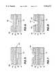
- FIG. 1illustrates a schematic depiction of a substrate containing a memory device which includes a memory matrix and peripheral circuitry;
- FIG. 2illustrates an exemplary schematic depiction of the memory matrix or array of FIG. 1;
- FIG. 3illustrates an exemplary memory cell having a memory element, such as a resistor, and an access device, such as a diode;
- FIG. 4illustrates a top view of a portion of a semiconductor memory array
- FIG. 5illustrates a cross-sectional view of an exemplary memory cell at an early stage of fabrication
- FIG. 6, FIG. 7, and FIG. 8illustrate the formation of a spacer and a small pore for the exemplary memory element
- FIG. 9illustrates the small pore of the memory element
- FIG. 10 and FIG. 11illustrate the formation of an electrode in the small pore
- FIG. 12illustrates the deposition of memory material over the lower electrode
- FIG. 13illustrates the deposition of the upper electrode of the memory cell
- FIG. 14illustrates the deposition of an insulative layer and an oxide layer over the upper electrode of the memory cell
- FIG. 15illustrates the formation of a contact extending through the oxide and insulative layer to contact the upper electrode.
- the memory device 10is an integrated circuit memory that is advantageously formed on a semiconductor substrate 12.
- the memory device 10includes a memory matrix or array 14 that includes a plurality of memory cells for storing data, as described below.
- the memory matrix 14is coupled to periphery circuitry 16 by the plurality of control lines 18.
- the periphery circuitry 16may include circuitry for addressing the memory cells contained within the memory matrix 14, along with circuitry for storing data in and retrieving data from the memory cells.
- the periphery circuitry 16may also include other circuitry used for controlling or otherwise insuring the proper functioning of the memory device 10.
- the memory matrix 14includes a plurality of memory cells 20 that are arranged in generally perpendicular rows and columns.
- the memory cells 20 in each roware coupled together by a respective word line 22, and the memory cells 20 in each column are coupled together by a respective digit line 24.
- each memory cell 20includes a word line node 26 that is coupled to a respective word line 22, and each memory cell 20 includes a digit line node 28 that is coupled to a respective digit line 24.
- the conductive word lines 22 and digit lines 24are collectively referred to as address lines. These address lines are electrically coupled to the periphery circuitry 16 so that each of the memory cells 20 can be accessed for the storage and retrieval of information.
- FIG. 3illustrates an exemplary memory cell 20 that may be used in the memory matrix 14.
- the memory cell 20includes a memory element 30 which is coupled to an access device 32.
- the memory element 30is illustrated as a programmable resistive element
- the access device 32is illustrated as a diode.
- the programmable resistive elementmay be made of a chalcogenide material, as will be more filly explained below.
- the diode 32may be a conventional diode, a zener diode, or an avalanche diode, depending upon whether the diode array of the memory matrix 14 is operated in a forward biased mode or a reverse biased mode.
- the memory element 30is coupled to a word line 22, and the access device 32 is coupled to a digit line 24.
- connections of the memory element 20may be reversed without adversely affecting the operation of the memory matrix 14.
- a chalcogenide resistormay be used as the memory element 30.
- a chalcogenide resistoris a structure changing memory element because its molecular order may be changed between an amorphous state and a crystalline state by the application of electrical current.
- a chalcogenide resistoris made of a state changeable material that can be switched from one detectable state to another detectable state or states.
- the detectable statesmay differ in their morphology, surface typography, relative degree of order, relative degree of disorder, electrical properties, optical properties, or combinations of one or more of these properties.
- the state of a state changeable materialmay be detected by measuring the electrical conductivity, electrical resistivity, optical transmissivity, optical absorption, optical refraction, optical reflectivity, or a combination of these properties.
- a chalcogenide resistorspecifically, it may be switched between different structural states of local order across the entire spectrum between the completely amorphous state and the completely crystalline state.
- the previously mentioned Ovshinsky patentcontains a graphical representation of the resistance of an exemplary chalcogenide resistor as a finction of voltage applied across the resistor. It is not unusal for a chalcogenide resistor to demonstrate a wide dynamic range of attainable resistance values of about two orders of magnitude. When the chalcogenide resistor is in its amorphous state, its resistance is relatively high. As the chalcogenide resistor changes to its crystalline state, its resistance decreases.
- chalcogenide resistorAs discussed in the Ovshinsky patent, low voltages do not alter the structure of a chalcogenide resistor, while higher voltages may alter its structure.
- a chalcogenide resistori.e., to place the chalcogenide resistor in a selected physical or resistive state
- a selected voltage in the range of higher voltagesis applied across the chalcogenide resistor, i.e., between the word line 22 and the digit line 24.
- a low voltagemay be applied to the chalcogenide resistor, i.e., between the word line 22 and the digit line 24, to determine its resistance without changing its physical state.
- the addressing, programming, and reading of the memory elements 20 and, thus, the application of particular voltages across the word lines 22 and digit lines 24,is facilitated by the periphery circuitry 16.
- the memory cell 20, as illustrated in FIG. 3,may offer significant packaging advantages as compared with memory cells used in traditional random access and read only memories. This advantage stems from the fact that the memory cell 20 is a vertically integrated device. In other words, the memory element 30 may be fabricated on top of the access device 32. Therefore, using the memory cell 20, it may be possible to fabricate an X-point cell that is the same size as the crossing area of the word line 22 and the digit line 24, as illustrated in FIG. 4. However, the size of the access device 32 typically limits the area of the memory cell 20, because the access device 32 must be large enough to handle the programming current needed by the memory element 30.
- the size of the active area of the chalcogenide memory element 30may be reduced by reducing the size of an electrode which borders the chalcogenide material. By reducing the active area and, thus, the required programming current, the size of the access device may be reduced to create an X-point cell memory.
- a cell with a chalcogenide cross-sectional area equivalent to a circle with an 0.2 ⁇ m diametermight require a current pulse of 2 ⁇ A to program to high resistance state. If the diameter of the cell is reduced to 0.1 ⁇ m the current could be reduced to about 0.5 mA. Over certain ranges of operation the programming current is directly proportional to the area of the cell.
- each memory cell 20is electrically isolated from other memory cells in the array in any suitable manner, such as by the addition imbedded field oxide regions between each memory cell.
- the digit lines 24are formed in or on a substrate 12. As illustrated in FIG. 5, the digit line 24 is formed in the P-type substrate 12 as a heavily doped N+ type trench. This trench may be strapped with appropriate materials to enhance its conductivity.
- the access device 32is formed on top of the digit line 24.
- the illustrated access device 32is a diode formed by a layer of N doped polysilicon 40 and a layer of P+ doped polysilicon 42.
- a layer of insulative or dielectric material 44is disposed on top of the P+ layer 42.
- the layer 44may be formed from any suitable insulative or dielectric material, such as plasma enhanced CVD SiO z , or PECVD silicon nitride or standard thermal CVD Sa 3 Ny.
- a hard mask 46is deposited on top of the dielectric layer 44 and patterned to form a window 48, as illustrated in FIG. 6.
- the window 48 in the hard mask 46is advantageously as small as possible.
- the window 48may be formed at the photolithographic limit by conventional photolithographic techniques.
- the photolithographic limiti.e., the smallest feature that can be patterned using photolithographic techniques, is currently about 0.2 ⁇ m.
- a layer of spacer material 50is deposited over the hard mask 46 in a conformal fashion so that the upper surface of the spacer material 50 is recessed where the spacer material 50 covers the window 48.
- a dielectric materialsuch CVD amorphous or polycrystalline silicon, may be advantageous.
- the layer of spacer material 50is subjected to an anisotropic etch using a suitable etchant, such as HBr+Cl 2 .
- a suitable etchantsuch as HBr+Cl 2 .
- the rate and time of the etchare controlled so that the layer of spacer material 50 is substantially removed from the upper surface of the hard mask 48 and from a portion of the upper surface of the dielectric layer 44 within the window 48, leaving sidewall spacers 52 within the window 48.
- the sidewall spacers 52remain after a properly controlled etch because the vertical dimension of the spacer material 50 near the sidewalls of the window 48 is approximately twice as great as the vertical dimension of the spacer material 50 on the surface of the hard mask 46 and in the recessed area of the window 48.
- an etchantis applied to the structure to form a pore 54 in the dielectric layer 44, as illustrated in FIG. 8.
- the etchantis an anisotropic etchant that selectively removes the material of the dielectric layer 44 bounded by the spacers 52 until the P+ layer 42 is reached.
- the window 48is at the photolithographic limit
- the pore 54is smaller than the photolithigraphic limit, e.g., on the order of 0.1 ⁇ m.
- the hard mask 46 and the spacers 52may be removed, as illustrated in FIG. 9.
- the hard mask 46 and the spacers 52may be removed by any suitable method, such as by etching or by chemical mechanical planarization (CMP).
- the pore 54is then filled to a desired level with a material suitable to form the lower electrode of the chalcogenide memory element 30.
- a layer of electrode material 56is deposited using collimated physical vapor deposition (PVD).
- PVDphysical vapor deposition
- the layer of electrode material 56is formed on top of the dielectric layer 44 and within the pore 54 with substantially no sidewalls.
- the layer of electrode material 56 on top of the dielectric layer 44may be removed, using CMP for instance, to leave the electrode 56 at the bottom of the pore 54, as illustrated in FIG. 11.
- the electrode material 56may be comprised of one or more materials, and it may be formed in one or more layers.
- a lower layer of carbonmay be used as a barrier layer to prevent unwanted migration between the subsequently deposited chalcogenide material and the P+ type layer 42.
- a layer of titanium nitride (TiN)may then be deposited upon the layer of carbon to complete the formation of the electrode 56.
- chalcogenide material 58may be deposited so that it contacts the lower electrode 56, as illustrated in FIG. 12.
- chalcogenide materialsmay be used to form the chalcogenide memory element 30.
- chalcogenide alloysmay be formed from tellurium, antimony, germanium, selenium, bismuth, lead, strontium, arsenic, sulfur, silicon, phosphorous, and oxygen.
- the particular alloy selectedshould be capable of assuming at least two generally stable states in response to a stimulus, for a binary memory, and capable of assuming multiple generally stable states in response to a stimulus, for a higher order memory.
- the stimuluswill be an electrical signal, and the multiple states will be different states of crystallinity having varying levels of electrical resistance.
- Alloys that may be particularly advantageousinclude tellurium, antimony, and germanium having approximately 55 to 85 percent tellurium and 15 to 25 percent germanium, such as Te 56 Ge 22 Sb 22 .
- any chalcogenide material 58 adjacent the pore 54 on the surface of the dielectric layer 44may be removed, using CMP for instance, to create a chalcogenide element of extremely small proportions.
- the chalcogenide material 58 adjacent the pore 54may remain, because the extremely small size of the lower electrode 56 still creates a relatively small active area in a vertical direction through the chalcogenide material 58. Because of this characteristic, even if the lower electrode 56 only partially fills the pore 54, as illustrated, the excess chalcogenide material 58 adjacent the pore 54 need not be removed to create a memory element 30 having an extremely small active area.
- the upper electrode 60is deposited on top of the chalcogenide material 58, as illustrated in FIG. 13.
- a layer of insulative material 62such as silicon nitride, is deposited over the structure, as illustrated in FIG. 14.
- a layer of oxide 64is then deposited over the insulative layer 62.
- the oxide layer 64is patterned and a contact hole 66 is formed through the oxide layer 64 and the insulative layer 62, as illustrated in FIG. 15.
- the contact hole 66is filled with a conductive material to form the word line 22.
Landscapes
- Engineering & Computer Science (AREA)
- Manufacturing & Machinery (AREA)
- Semiconductor Memories (AREA)
Abstract
Description
Claims (15)
Priority Applications (6)
| Application Number | Priority Date | Filing Date | Title |
|---|---|---|---|
| US08/854,220US5952671A (en) | 1997-05-09 | 1997-05-09 | Small electrode for a chalcogenide switching device and method for fabricating same |
| US09/344,604US6189582B1 (en) | 1997-05-09 | 1999-06-25 | Small electrode for a chalcogenide switching device and method for fabricating same |
| US09/740,256US6777705B2 (en) | 1997-05-09 | 2000-12-19 | X-point memory cell |
| US10/872,765US7102151B2 (en) | 1997-05-09 | 2004-06-21 | Small electrode for a chalcogenide switching device and method for fabricating same |
| US11/494,052US7453082B2 (en) | 1997-05-09 | 2006-07-27 | Small electrode for a chalcogenide switching device and method for fabricating same |
| US11/929,331US20080055973A1 (en) | 1997-05-09 | 2007-10-30 | Small Electrode for a Chacogenide Switching Device and Method for Fabricating Same |
Applications Claiming Priority (1)
| Application Number | Priority Date | Filing Date | Title |
|---|---|---|---|
| US08/854,220US5952671A (en) | 1997-05-09 | 1997-05-09 | Small electrode for a chalcogenide switching device and method for fabricating same |
Related Child Applications (1)
| Application Number | Title | Priority Date | Filing Date |
|---|---|---|---|
| US09/344,604DivisionUS6189582B1 (en) | 1997-05-09 | 1999-06-25 | Small electrode for a chalcogenide switching device and method for fabricating same |
Publications (1)
| Publication Number | Publication Date |
|---|---|
| US5952671Atrue US5952671A (en) | 1999-09-14 |
Family
ID=25318069
Family Applications (6)
| Application Number | Title | Priority Date | Filing Date |
|---|---|---|---|
| US08/854,220Expired - LifetimeUS5952671A (en) | 1997-05-09 | 1997-05-09 | Small electrode for a chalcogenide switching device and method for fabricating same |
| US09/344,604Expired - LifetimeUS6189582B1 (en) | 1997-05-09 | 1999-06-25 | Small electrode for a chalcogenide switching device and method for fabricating same |
| US09/740,256Expired - Fee RelatedUS6777705B2 (en) | 1997-05-09 | 2000-12-19 | X-point memory cell |
| US10/872,765Expired - Fee RelatedUS7102151B2 (en) | 1997-05-09 | 2004-06-21 | Small electrode for a chalcogenide switching device and method for fabricating same |
| US11/494,052Expired - Fee RelatedUS7453082B2 (en) | 1997-05-09 | 2006-07-27 | Small electrode for a chalcogenide switching device and method for fabricating same |
| US11/929,331AbandonedUS20080055973A1 (en) | 1997-05-09 | 2007-10-30 | Small Electrode for a Chacogenide Switching Device and Method for Fabricating Same |
Family Applications After (5)
| Application Number | Title | Priority Date | Filing Date |
|---|---|---|---|
| US09/344,604Expired - LifetimeUS6189582B1 (en) | 1997-05-09 | 1999-06-25 | Small electrode for a chalcogenide switching device and method for fabricating same |
| US09/740,256Expired - Fee RelatedUS6777705B2 (en) | 1997-05-09 | 2000-12-19 | X-point memory cell |
| US10/872,765Expired - Fee RelatedUS7102151B2 (en) | 1997-05-09 | 2004-06-21 | Small electrode for a chalcogenide switching device and method for fabricating same |
| US11/494,052Expired - Fee RelatedUS7453082B2 (en) | 1997-05-09 | 2006-07-27 | Small electrode for a chalcogenide switching device and method for fabricating same |
| US11/929,331AbandonedUS20080055973A1 (en) | 1997-05-09 | 2007-10-30 | Small Electrode for a Chacogenide Switching Device and Method for Fabricating Same |
Country Status (1)
| Country | Link |
|---|---|
| US (6) | US5952671A (en) |
Cited By (198)
| Publication number | Priority date | Publication date | Assignee | Title |
|---|---|---|---|---|
| US6236587B1 (en)* | 1997-09-01 | 2001-05-22 | Thin Film Electronics Asa | Read-only memory and read-only memory devices |
| US20020017701A1 (en)* | 1999-03-25 | 2002-02-14 | Patrick Klersy | Electrically programmable memory element with raised pore |
| US20020018355A1 (en)* | 1998-11-16 | 2002-02-14 | Johnson Mark G. | Vertically stacked field programmable nonvolatile memory and method of fabrication |
| US20020195621A1 (en)* | 2001-06-26 | 2002-12-26 | Jon Maimon | Programmable resistance memory element and method for making same |
| US20030071289A1 (en)* | 2001-08-31 | 2003-04-17 | Hudgens Stephen J. | Multiple layer phase-change memory |
| US20030082908A1 (en)* | 2001-10-30 | 2003-05-01 | Lowrey Tyler A. | Phase change material memory device |
| US6579760B1 (en) | 2002-03-28 | 2003-06-17 | Macronix International Co., Ltd. | Self-aligned, programmable phase change memory |
| US20030155589A1 (en)* | 2002-02-20 | 2003-08-21 | Campbell Kristy A. | Silver-selenide/chalcogenide glass stack for resistance variable memory |
| US6613604B2 (en)* | 2001-08-02 | 2003-09-02 | Ovonyx, Inc. | Method for making small pore for use in programmable resistance memory element |
| WO2003067633A3 (en)* | 2002-02-08 | 2003-10-16 | Ovonyx Inc | Programmable resistance memory element and method for making same |
| US20030214856A1 (en)* | 2002-02-20 | 2003-11-20 | Stmicroelectronics S. R. I. | Contact structure, phase change memory cell, and manufacturing method thereof with elimination of double contacts |
| US20040012009A1 (en)* | 2002-02-20 | 2004-01-22 | Stmicroelectronics S.R.L. | Sublithographic contact structure, phase change memory cell with optimized heater shape, and manufacturing method thereof |
| US20040042298A1 (en)* | 2002-08-20 | 2004-03-04 | Horii Hideki | Phase changeable memory devices having reduced cell areas |
| US20040043137A1 (en)* | 2002-08-09 | 2004-03-04 | Macronix International Co., Ltd. | Spacer chalcogenide memory method and device |
| US6709958B2 (en) | 2001-08-30 | 2004-03-23 | Micron Technology, Inc. | Integrated circuit device and fabrication using metal-doped chalcogenide materials |
| WO2003079443A3 (en)* | 2002-03-14 | 2004-04-01 | Micron Technology Inc | Manufacturing methods for resistance variable material cells |
| US20040124407A1 (en)* | 2000-02-11 | 2004-07-01 | Kozicki Michael N. | Scalable programmable structure, an array including the structure, and methods of forming the same |
| KR100448908B1 (en)* | 2002-09-03 | 2004-09-16 | 삼성전자주식회사 | Phase-changeable memory device structure and method for fabricating the same |
| US20040211953A1 (en)* | 2003-01-15 | 2004-10-28 | Stmicroelectronics S.R.L. | Sublithographic contact structure, in particular for a phase change memory cell, and fabrication process thereof |
| US20050001284A1 (en)* | 2001-12-05 | 2005-01-06 | Stmicroelectronics S.R.L. | Self-aligned process for manufacturing a phase change memory cell and phase change memory cell thereby manufactured |
| US20050064606A1 (en)* | 2003-08-05 | 2005-03-24 | Stmicroelectronics S.R.I. | Process for manufacturing a phase change memory array in Cu-damascene technology and phase change memory array manufactured thereby |
| US6891747B2 (en) | 2002-02-20 | 2005-05-10 | Stmicroelectronics S.R.L. | Phase change memory cell and manufacturing method thereof using minitrenches |
| US6916696B1 (en)* | 2003-11-20 | 2005-07-12 | Advanced Micro Devices, Inc. | Method for manufacturing a memory element |
| US20050185444A1 (en)* | 2004-02-25 | 2005-08-25 | Soo-Guil Yang | Phase-changeable memory device and method of manufacturing the same |
| US20050263823A1 (en)* | 2004-05-27 | 2005-12-01 | Young-Nam Hwang | Phase-change memory device having a barrier layer and manufacturing method |
| US20050263801A1 (en)* | 2004-05-27 | 2005-12-01 | Jae-Hyun Park | Phase-change memory device having a barrier layer and manufacturing method |
| US20050263829A1 (en)* | 2004-05-27 | 2005-12-01 | Yoon-Jong Song | Semiconductor devices having phase change memory cells, electronic systems employing the same and methods of fabricating the same |
| JP2005340837A (en)* | 2004-05-27 | 2005-12-08 | Samsung Electronics Co Ltd | Semiconductor device having phase change memory element covered with oxygen barrier film, electronic system using the same, and method of manufacturing the same |
| US20050281075A1 (en)* | 2004-06-17 | 2005-12-22 | Zhizhang Chen | Semiconductor storage device |
| US20060108667A1 (en)* | 2004-11-22 | 2006-05-25 | Macronix International Co., Ltd. | Method for manufacturing a small pin on integrated circuits or other devices |
| US20060126424A1 (en)* | 2003-11-12 | 2006-06-15 | Ryu Ogiwara | Phase-change memory device using chalcogenide compound as the material of memory cells |
| US20060124916A1 (en)* | 2004-12-09 | 2006-06-15 | Macronix International Co., Ltd. | Self-aligned small contact phase-change memory method and device |
| WO2006076378A1 (en)* | 2005-01-11 | 2006-07-20 | Ovonyx, Inc. | Programmable matrix array with chalcogenide material |
| US20060284158A1 (en)* | 2005-06-17 | 2006-12-21 | Macronix International Co., Ltd. | Self-aligned, embedded phase change ram and manufacturing method |
| US20060284214A1 (en)* | 2005-06-17 | 2006-12-21 | Macronix International Co., Ltd. | Thin film fuse phase change cell with thermal isolation layer and manufacturing method |
| US20060286709A1 (en)* | 2005-06-17 | 2006-12-21 | Macronix International Co., Ltd. | Manufacturing methods for thin film fuse phase change ram |
| US20060284279A1 (en)* | 2005-06-17 | 2006-12-21 | Macronix International Co., Ltd. | Thin film fuse phase change RAM and manufacturing method |
| US20060286743A1 (en)* | 2005-06-17 | 2006-12-21 | Macronix International Co., Ltd. | Method for Manufacturing a Narrow Structure on an Integrated Circuit |
| US20060284157A1 (en)* | 2005-06-17 | 2006-12-21 | Macronix International Co., Ltd. | Thin film plate phase change RAM circuit and manufacturing method |
| US20070108430A1 (en)* | 2005-11-15 | 2007-05-17 | Macronix International Co., Ltd. | Thermally contained/insulated phase change memory device and method (combined) |
| US20070111429A1 (en)* | 2005-11-14 | 2007-05-17 | Macronix International Co., Ltd. | Method of manufacturing a pipe shaped phase change memory |
| US20070108429A1 (en)* | 2005-11-14 | 2007-05-17 | Macronix International Co., Ltd. | Pipe shaped phase change memory |
| US20070109843A1 (en)* | 2005-11-15 | 2007-05-17 | Macronix International Co., Ltd. | Phase Change Memory Device and Manufacturing Method |
| US20070121363A1 (en)* | 2005-11-28 | 2007-05-31 | Macronix International Co., Ltd. | Phase Change Memory Cell and Manufacturing Method |
| US7227171B2 (en) | 2001-12-05 | 2007-06-05 | Stmicroelectronics S.R.L. | Small area contact region, high efficiency phase change memory cell and fabrication method thereof |
| US20070131922A1 (en)* | 2005-12-13 | 2007-06-14 | Macronix International Co., Ltd. | Thin Film Fuse Phase Change Cell with Thermal Isolation Pad and Manufacturing Method |
| US20070131980A1 (en)* | 2005-11-21 | 2007-06-14 | Lung Hsiang L | Vacuum jacket for phase change memory element |
| US20070148814A1 (en)* | 2005-12-22 | 2007-06-28 | Stmicroelectronics S.R.L. | Process for manufacturing a phase change memory array in Cu-damascene technology and phase change memory array thereby manufactured |
| US20070154847A1 (en)* | 2005-12-30 | 2007-07-05 | Macronix International Co., Ltd. | Chalcogenide layer etching method |
| US20070155172A1 (en)* | 2005-12-05 | 2007-07-05 | Macronix International Co., Ltd. | Manufacturing Method for Phase Change RAM with Electrode Layer Process |
| US20070158645A1 (en)* | 2006-01-11 | 2007-07-12 | Macronix International Co., Ltd. | Self-align planerized bottom electrode phase change memory and manufacturing method |
| US20070158690A1 (en)* | 2006-01-09 | 2007-07-12 | Macronix International Co., Ltd. | Programmable Resistive RAM and Manufacturing Method |
| US20070161186A1 (en)* | 2006-01-09 | 2007-07-12 | Macronix International Co., Ltd. | Programmable Resistive RAM and Manufacturing Method |
| US20070176261A1 (en)* | 2006-01-30 | 2007-08-02 | Macronix International Co., Ltd. | Vertical Side Wall Active Pin Structures in a Phase Change Memory and Manufacturing Methods |
| US20070241371A1 (en)* | 2006-04-17 | 2007-10-18 | Macronix International Co., Ltd. | Memory device and manufacturing method |
| US20070257300A1 (en)* | 2006-05-05 | 2007-11-08 | Macronix International Co., Ltd. | Structures and Methods of a Bistable Resistive Random Access Memory |
| US20070262388A1 (en)* | 2006-05-09 | 2007-11-15 | Macronix International Co., Ltd. | Bridge Resistance Random Access Memory Device and Method With A Singular Contact Structure |
| US20070274121A1 (en)* | 2005-06-17 | 2007-11-29 | Macronix International Co., Ltd. | Multi-level memory cell having phase change element and asymmetrical thermal boundary |
| US20070278529A1 (en)* | 2006-05-30 | 2007-12-06 | Macronix International Co., Ltd. | Resistor random access memory cell with l-shaped electrode |
| US20070281420A1 (en)* | 2006-05-30 | 2007-12-06 | Macronix International Co., Ltd. | Resistor random access memory cell with reduced active area and reduced contact areas |
| US20070290185A1 (en)* | 2006-06-15 | 2007-12-20 | Industrial Technology Research Institute | Phase change memory cells and methods for fabricating the same |
| US20080043520A1 (en)* | 2006-02-07 | 2008-02-21 | Chen Shih H | I-shaped phase change memory cell with thermal isolation |
| US20080048213A1 (en)* | 2006-08-25 | 2008-02-28 | Jun Liu | Self-aligned, planar phase change memory elements and devices, systems employing the same and methods of forming the same |
| US20080055973A1 (en)* | 1997-05-09 | 2008-03-06 | Micron Technology Inc. | Small Electrode for a Chacogenide Switching Device and Method for Fabricating Same |
| US20080096375A1 (en)* | 2006-10-18 | 2008-04-24 | Macronix International Co., Ltd. | Method for Making Memory Cell Device |
| US20080094885A1 (en)* | 2006-10-24 | 2008-04-24 | Macronix International Co., Ltd. | Bistable Resistance Random Access Memory Structures with Multiple Memory Layers and Multilevel Memory States |
| US20080099791A1 (en)* | 2006-10-04 | 2008-05-01 | Macronix International Co., Ltd. | Memory Cell Device with Circumferentially-Extending Memory Element |
| US20080116440A1 (en)* | 2006-11-16 | 2008-05-22 | Macronix International Co., Ltd. | Resistance Random Access Memory Structure for Enhanced Retention |
| US20080119007A1 (en)* | 2006-11-16 | 2008-05-22 | Usha Raghuram | Method of making a nonvolatile phase change memory cell having a reduced contact area |
| US20080116441A1 (en)* | 2006-11-16 | 2008-05-22 | Usha Raghuram | Nonvolatile phase change memory cell having a reduced contact area |
| US20080121861A1 (en)* | 2006-08-16 | 2008-05-29 | Macronix International Co., Ltd. | Self-Aligned Structure and Method for Confining a Melting Point in a Resistor Random Access Memory |
| US20080138929A1 (en)* | 2006-12-06 | 2008-06-12 | Macronix International Co., Ltd. | Method for Making a Self-Converged Memory Material Element for Memory Cell |
| US20080138931A1 (en)* | 2006-12-06 | 2008-06-12 | Macronix International Co., Ltd. | Method for Making a Self-Converged Void and Bottom Electrode for Memoery Cell |
| US20080135824A1 (en)* | 2006-12-07 | 2008-06-12 | Macronix International Co., Ltd. | Method and Structure of a Multi-Level Cell Resistance Random Access Memory with Metal Oxides |
| US7388771B2 (en) | 2006-10-24 | 2008-06-17 | Macronix International Co., Ltd. | Methods of operating a bistable resistance random access memory with multiple memory layers and multilevel memory states |
| US20080157053A1 (en)* | 2006-12-28 | 2008-07-03 | Macronix International Co., Ltd. | Resistor Random Access Memory Cell Device |
| US20080165570A1 (en)* | 2007-01-05 | 2008-07-10 | Macronix International Co., Ltd. | Current Compliant Sensing Architecture for Multilevel Phase Change Memory |
| US20080165571A1 (en)* | 2007-01-09 | 2008-07-10 | Macronix International Co., Ltd. | Method, Apparatus and Computer Program Product for Read Before Programming Process on Multiple Programmable Resistive Memory Cell |
| CN100403405C (en)* | 2004-10-21 | 2008-07-16 | 株式会社日立制作所 | phase change memory |
| US20080186761A1 (en)* | 2007-02-07 | 2008-08-07 | Macronix International Co., Ltd. | Memory Cell with Separate Read and Program Paths |
| US7414258B2 (en) | 2005-11-16 | 2008-08-19 | Macronix International Co., Ltd. | Spacer electrode small pin phase change memory RAM and manufacturing method |
| US20080197334A1 (en)* | 2007-02-21 | 2008-08-21 | Macronix International Co., Ltd. | Phase Change Memory Cell with Heater and Method for Fabricating the Same |
| US20080197333A1 (en)* | 2007-02-21 | 2008-08-21 | Macronix International Co., Ltd. | Programmable Resistive Memory Cell with Self-Forming Gap |
| US20080203375A1 (en)* | 2007-02-27 | 2008-08-28 | Macronix International Co., Ltd. | Memory Cell with Memory Element Contacting Ring-Shaped Upper End of Bottom Electrode |
| US7423300B2 (en) | 2006-05-24 | 2008-09-09 | Macronix International Co., Ltd. | Single-mask phase change memory element |
| US7432206B2 (en) | 2006-01-24 | 2008-10-07 | Macronix International Co., Ltd. | Self-aligned manufacturing method, and manufacturing method for thin film fuse phase change ram |
| US20080246014A1 (en)* | 2007-04-03 | 2008-10-09 | Macronix International Co., Ltd. | Memory Structure with Reduced-Size Memory Element Between Memory Material Portions |
| US20080247224A1 (en)* | 2007-04-06 | 2008-10-09 | Macronix International Co., Ltd. | Phase Change Memory Bridge Cell with Diode Isolation Device |
| US7440315B2 (en) | 2007-01-09 | 2008-10-21 | Macronix International Co., Ltd. | Method, apparatus and computer program product for stepped reset programming process on programmable resistive memory cell |
| US20080259672A1 (en)* | 2007-04-17 | 2008-10-23 | Macronix International Co., Ltd. | 4f2 self align side wall active phase change memory |
| US20080266933A1 (en)* | 2007-04-24 | 2008-10-30 | Macronix International Co., Ltd. | Method and Apparatus for Refreshing Programmable Resistive Memory |
| US7450411B2 (en) | 2005-11-15 | 2008-11-11 | Macronix International Co., Ltd. | Phase change memory device and manufacturing method |
| US7463512B2 (en) | 2007-02-08 | 2008-12-09 | Macronix International Co., Ltd. | Memory element with reduced-current phase change element |
| US20090014706A1 (en)* | 2007-07-13 | 2009-01-15 | Macronix International Co., Ltd. | 4f2 self align fin bottom electrodes fet drive phase change memory |
| US7479649B2 (en) | 2005-11-21 | 2009-01-20 | Macronix International Co., Ltd. | Vacuum jacketed electrode for phase change memory element |
| US20090032793A1 (en)* | 2007-08-03 | 2009-02-05 | Macronix International Co., Ltd. | Resistor Random Access Memory Structure Having a Defined Small Area of Electrical Contact |
| US7507986B2 (en) | 2005-11-21 | 2009-03-24 | Macronix International Co., Ltd. | Thermal isolation for an active-sidewall phase change memory cell |
| US7521364B2 (en) | 2005-12-02 | 2009-04-21 | Macronix Internation Co., Ltd. | Surface topology improvement method for plug surface areas |
| US7527985B2 (en) | 2006-10-24 | 2009-05-05 | Macronix International Co., Ltd. | Method for manufacturing a resistor random access memory with reduced active area and reduced contact areas |
| US7531825B2 (en) | 2005-12-27 | 2009-05-12 | Macronix International Co., Ltd. | Method for forming self-aligned thermal isolation cell for a variable resistance memory array |
| US7535756B2 (en) | 2007-01-31 | 2009-05-19 | Macronix International Co., Ltd. | Method to tighten set distribution for PCRAM |
| US7534647B2 (en) | 2005-06-17 | 2009-05-19 | Macronix International Co., Ltd. | Damascene phase change RAM and manufacturing method |
| US7551473B2 (en) | 2007-10-12 | 2009-06-23 | Macronix International Co., Ltd. | Programmable resistive memory with diode structure |
| US7560337B2 (en) | 2006-01-09 | 2009-07-14 | Macronix International Co., Ltd. | Programmable resistive RAM and manufacturing method |
| US7569844B2 (en) | 2007-04-17 | 2009-08-04 | Macronix International Co., Ltd. | Memory cell sidewall contacting side electrode |
| US20090194839A1 (en)* | 2005-11-15 | 2009-08-06 | Bertin Claude L | Nonvolatile nanotube diodes and nonvolatile nanotube blocks and systems using same and methods of making same |
| US7599217B2 (en) | 2005-11-22 | 2009-10-06 | Macronix International Co., Ltd. | Memory cell device and manufacturing method |
| US7619311B2 (en) | 2007-02-02 | 2009-11-17 | Macronix International Co., Ltd. | Memory cell device with coplanar electrode surface and method |
| US7635855B2 (en) | 2005-11-15 | 2009-12-22 | Macronix International Co., Ltd. | I-shaped phase change memory cell |
| US7639527B2 (en) | 2008-01-07 | 2009-12-29 | Macronix International Co., Ltd. | Phase change memory dynamic resistance test and manufacturing methods |
| US7642125B2 (en) | 2007-09-14 | 2010-01-05 | Macronix International Co., Ltd. | Phase change memory cell in via array with self-aligned, self-converged bottom electrode and method for manufacturing |
| US7646631B2 (en) | 2007-12-07 | 2010-01-12 | Macronix International Co., Ltd. | Phase change memory cell having interface structures with essentially equal thermal impedances and manufacturing methods |
| US7663135B2 (en) | 2007-01-31 | 2010-02-16 | Macronix International Co., Ltd. | Memory cell having a side electrode contact |
| US7682868B2 (en) | 2006-12-06 | 2010-03-23 | Macronix International Co., Ltd. | Method for making a keyhole opening during the manufacture of a memory cell |
| US7688619B2 (en) | 2005-11-28 | 2010-03-30 | Macronix International Co., Ltd. | Phase change memory cell and manufacturing method |
| US7696506B2 (en) | 2006-06-27 | 2010-04-13 | Macronix International Co., Ltd. | Memory cell with memory material insulation and manufacturing method |
| US7701750B2 (en) | 2008-05-08 | 2010-04-20 | Macronix International Co., Ltd. | Phase change device having two or more substantial amorphous regions in high resistance state |
| US7701759B2 (en) | 2007-02-05 | 2010-04-20 | Macronix International Co., Ltd. | Memory cell device and programming methods |
| US7719913B2 (en) | 2008-09-12 | 2010-05-18 | Macronix International Co., Ltd. | Sensing circuit for PCRAM applications |
| US7729161B2 (en) | 2007-08-02 | 2010-06-01 | Macronix International Co., Ltd. | Phase change memory with dual word lines and source lines and method of operating same |
| US20100177553A1 (en)* | 2009-01-14 | 2010-07-15 | Macronix International Co., Ltd. | Rewritable memory device |
| US7772581B2 (en) | 2006-09-11 | 2010-08-10 | Macronix International Co., Ltd. | Memory device having wide area phase change element and small electrode contact area |
| US7777215B2 (en) | 2007-07-20 | 2010-08-17 | Macronix International Co., Ltd. | Resistive memory structure with buffer layer |
| US7785920B2 (en) | 2006-07-12 | 2010-08-31 | Macronix International Co., Ltd. | Method for making a pillar-type phase change memory element |
| US7791057B2 (en) | 2008-04-22 | 2010-09-07 | Macronix International Co., Ltd. | Memory cell having a buried phase change region and method for fabricating the same |
| US7804083B2 (en) | 2007-11-14 | 2010-09-28 | Macronix International Co., Ltd. | Phase change memory cell including a thermal protect bottom electrode and manufacturing methods |
| US7816661B2 (en) | 2005-11-21 | 2010-10-19 | Macronix International Co., Ltd. | Air cell thermal isolation for a memory array formed of a programmable resistive material |
| US7825398B2 (en) | 2008-04-07 | 2010-11-02 | Macronix International Co., Ltd. | Memory cell having improved mechanical stability |
| US7829876B2 (en) | 2005-11-21 | 2010-11-09 | Macronix International Co., Ltd. | Vacuum cell thermal isolation for a phase change memory device |
| US20100321987A1 (en)* | 2009-06-22 | 2010-12-23 | Macronix International Co., Ltd. | Memory device and method for sensing and fixing margin cells |
| US20100328995A1 (en)* | 2009-06-25 | 2010-12-30 | Macronix International Co., Ltd. | Methods and apparatus for reducing defect bits in phase change memory |
| US20100328996A1 (en)* | 2009-06-25 | 2010-12-30 | Macronix International Co., Ltd. | Phase change memory having one or more non-constant doping profiles |
| US7863655B2 (en) | 2006-10-24 | 2011-01-04 | Macronix International Co., Ltd. | Phase change memory cells with dual access devices |
| US7869270B2 (en) | 2008-12-29 | 2011-01-11 | Macronix International Co., Ltd. | Set algorithm for phase change memory cell |
| US20110012083A1 (en)* | 2009-07-15 | 2011-01-20 | Macronix International Co., Ltd. | Phase change memory cell structure |
| US20110012079A1 (en)* | 2009-07-15 | 2011-01-20 | Macronix International Co., Ltd. | Thermal protect pcram structure and methods for making |
| US20110013446A1 (en)* | 2009-07-15 | 2011-01-20 | Macronix International Co., Ltd. | Refresh circuitry for phase change memory |
| US7879645B2 (en) | 2008-01-28 | 2011-02-01 | Macronix International Co., Ltd. | Fill-in etching free pore device |
| US7879643B2 (en) | 2008-01-18 | 2011-02-01 | Macronix International Co., Ltd. | Memory cell with memory element contacting an inverted T-shaped bottom electrode |
| US7884343B2 (en) | 2007-02-14 | 2011-02-08 | Macronix International Co., Ltd. | Phase change memory cell with filled sidewall memory element and method for fabricating the same |
| US7884342B2 (en) | 2007-07-31 | 2011-02-08 | Macronix International Co., Ltd. | Phase change memory bridge cell |
| US7897954B2 (en) | 2008-10-10 | 2011-03-01 | Macronix International Co., Ltd. | Dielectric-sandwiched pillar memory device |
| US20110049456A1 (en)* | 2009-09-03 | 2011-03-03 | Macronix International Co., Ltd. | Phase change structure with composite doping for phase change memory |
| US7903457B2 (en) | 2008-08-19 | 2011-03-08 | Macronix International Co., Ltd. | Multiple phase change materials in an integrated circuit for system on a chip application |
| US7903447B2 (en) | 2006-12-13 | 2011-03-08 | Macronix International Co., Ltd. | Method, apparatus and computer program product for read before programming process on programmable resistive memory cell |
| US20110063902A1 (en)* | 2009-09-17 | 2011-03-17 | Macronix International Co., Ltd. | 2t2r-1t1r mix mode phase change memory array |
| US7910907B2 (en) | 2006-03-15 | 2011-03-22 | Macronix International Co., Ltd. | Manufacturing method for pipe-shaped electrode phase change memory |
| US7919766B2 (en) | 2007-10-22 | 2011-04-05 | Macronix International Co., Ltd. | Method for making self aligning pillar memory cell device |
| US7928421B2 (en) | 2006-04-21 | 2011-04-19 | Macronix International Co., Ltd. | Phase change memory cell with vacuum spacer |
| US7933139B2 (en) | 2009-05-15 | 2011-04-26 | Macronix International Co., Ltd. | One-transistor, one-resistor, one-capacitor phase change memory |
| US7932506B2 (en) | 2008-07-22 | 2011-04-26 | Macronix International Co., Ltd. | Fully self-aligned pore-type memory cell having diode access device |
| US20110095257A1 (en)* | 2009-10-23 | 2011-04-28 | Huiwen Xu | Memory cell that includes a carbon-based reversible resistance switching element compatible with a steering element, and methods of forming the same |
| US20110095258A1 (en)* | 2009-10-23 | 2011-04-28 | Huiwen Xu | Memory cell that includes a carbon-based reversible resistance switching element compatible with a steering element, and methods of forming the same |
| US20110097825A1 (en)* | 2009-10-23 | 2011-04-28 | Macronix International Co., Ltd. | Methods For Reducing Recrystallization Time for a Phase Change Material |
| US20110133151A1 (en)* | 2009-12-07 | 2011-06-09 | Sandisk 3D Llc | Memory cell that includes a carbon-based memory element and methods of forming the same |
| US7968876B2 (en) | 2009-05-22 | 2011-06-28 | Macronix International Co., Ltd. | Phase change memory cell having vertical channel access transistor |
| US20110193042A1 (en)* | 2010-02-11 | 2011-08-11 | Steven Maxwell | Memory cell formed using a recess and methods for forming the same |
| US20110204474A1 (en)* | 2010-02-24 | 2011-08-25 | Franz Kreupl | Memory cell with silicon-containing carbon switching layer and methods for forming the same |
| US20110210306A1 (en)* | 2010-02-26 | 2011-09-01 | Yubao Li | Memory cell that includes a carbon-based memory element and methods of forming the same |
| US8030634B2 (en) | 2008-03-31 | 2011-10-04 | Macronix International Co., Ltd. | Memory array with diode driver and method for fabricating the same |
| US8030635B2 (en) | 2009-01-13 | 2011-10-04 | Macronix International Co., Ltd. | Polysilicon plug bipolar transistor for phase change memory |
| US8036014B2 (en) | 2008-11-06 | 2011-10-11 | Macronix International Co., Ltd. | Phase change memory program method without over-reset |
| US8077505B2 (en) | 2008-05-07 | 2011-12-13 | Macronix International Co., Ltd. | Bipolar switching of phase change device |
| US8084842B2 (en) | 2008-03-25 | 2011-12-27 | Macronix International Co., Ltd. | Thermally stabilized electrode structure |
| US8084760B2 (en) | 2009-04-20 | 2011-12-27 | Macronix International Co., Ltd. | Ring-shaped electrode and manufacturing method for same |
| US8089137B2 (en) | 2009-01-07 | 2012-01-03 | Macronix International Co., Ltd. | Integrated circuit memory with single crystal silicon on silicide driver and manufacturing method |
| US8097871B2 (en) | 2009-04-30 | 2012-01-17 | Macronix International Co., Ltd. | Low operational current phase change memory structures |
| US8107283B2 (en) | 2009-01-12 | 2012-01-31 | Macronix International Co., Ltd. | Method for setting PCRAM devices |
| US8134857B2 (en) | 2008-06-27 | 2012-03-13 | Macronix International Co., Ltd. | Methods for high speed reading operation of phase change memory and device employing same |
| US8138028B2 (en) | 2007-02-12 | 2012-03-20 | Macronix International Co., Ltd | Method for manufacturing a phase change memory device with pillar bottom electrode |
| US8158965B2 (en) | 2008-02-05 | 2012-04-17 | Macronix International Co., Ltd. | Heating center PCRAM structure and methods for making |
| US8173987B2 (en) | 2009-04-27 | 2012-05-08 | Macronix International Co., Ltd. | Integrated circuit 3D phase change memory array and manufacturing method |
| US8178386B2 (en) | 2007-09-14 | 2012-05-15 | Macronix International Co., Ltd. | Phase change memory cell array with self-converged bottom electrode and method for manufacturing |
| US8310864B2 (en) | 2010-06-15 | 2012-11-13 | Macronix International Co., Ltd. | Self-aligned bit line under word line memory array |
| US8324681B2 (en) | 2005-12-09 | 2012-12-04 | Macronix International Co., Ltd. | Stacked non-volatile memory device and methods for fabricating the same |
| US8324605B2 (en) | 2008-10-02 | 2012-12-04 | Macronix International Co., Ltd. | Dielectric mesh isolated phase change structure for phase change memory |
| US8344347B2 (en) | 2006-12-15 | 2013-01-01 | Macronix International Co., Ltd. | Multi-layer electrode structure |
| US8350316B2 (en) | 2009-05-22 | 2013-01-08 | Macronix International Co., Ltd. | Phase change memory cells having vertical channel access transistor and memory plane |
| US8395935B2 (en) | 2010-10-06 | 2013-03-12 | Macronix International Co., Ltd. | Cross-point self-aligned reduced cell size phase change memory |
| US8415651B2 (en) | 2008-06-12 | 2013-04-09 | Macronix International Co., Ltd. | Phase change memory cell having top and bottom sidewall contacts |
| US8467238B2 (en) | 2010-11-15 | 2013-06-18 | Macronix International Co., Ltd. | Dynamic pulse operation for phase change memory |
| US8471360B2 (en) | 2010-04-14 | 2013-06-25 | Sandisk 3D Llc | Memory cell with carbon switching material having a reduced cross-sectional area and methods for forming the same |
| US8497705B2 (en) | 2010-11-09 | 2013-07-30 | Macronix International Co., Ltd. | Phase change device for interconnection of programmable logic device |
| US8575719B2 (en) | 2000-04-28 | 2013-11-05 | Sandisk 3D Llc | Silicon nitride antifuse for use in diode-antifuse memory arrays |
| US8664689B2 (en) | 2008-11-07 | 2014-03-04 | Macronix International Co., Ltd. | Memory cell access device having a pn-junction with polycrystalline plug and single-crystal semiconductor regions |
| US8729521B2 (en) | 2010-05-12 | 2014-05-20 | Macronix International Co., Ltd. | Self aligned fin-type programmable memory cell |
| US8809829B2 (en) | 2009-06-15 | 2014-08-19 | Macronix International Co., Ltd. | Phase change memory having stabilized microstructure and manufacturing method |
| US8907316B2 (en) | 2008-11-07 | 2014-12-09 | Macronix International Co., Ltd. | Memory cell access device having a pn-junction with polycrystalline and single crystal semiconductor regions |
| US8933536B2 (en) | 2009-01-22 | 2015-01-13 | Macronix International Co., Ltd. | Polysilicon pillar bipolar transistor with self-aligned memory element |
| TWI470628B (en)* | 2005-12-24 | 2015-01-21 | Ovonyx Inc | Programmable matrix array with chalcogenide material |
| USRE45356E1 (en)* | 2005-09-07 | 2015-02-03 | Electronics And Telecommunications Research Institute | Phase-change memory device using Sb-Se metal alloy and method of fabricating the same |
| US8987700B2 (en) | 2011-12-02 | 2015-03-24 | Macronix International Co., Ltd. | Thermally confined electrode for programmable resistance memory |
| US9159412B1 (en) | 2014-07-15 | 2015-10-13 | Macronix International Co., Ltd. | Staggered write and verify for phase change memory |
| US9269746B2 (en)* | 2013-11-12 | 2016-02-23 | Samsung Electronics Co., Ltd. | Semiconductor devices and methods of manufacturing the same |
| US9336879B2 (en) | 2014-01-24 | 2016-05-10 | Macronix International Co., Ltd. | Multiple phase change materials in an integrated circuit for system on a chip application |
| US9559113B2 (en) | 2014-05-01 | 2017-01-31 | Macronix International Co., Ltd. | SSL/GSL gate oxide in 3D vertical channel NAND |
| US9672906B2 (en) | 2015-06-19 | 2017-06-06 | Macronix International Co., Ltd. | Phase change memory with inter-granular switching |
| CN108630723A (en)* | 2013-06-03 | 2018-10-09 | 美光科技公司 | Heat optimization phase-changing memory unit and its manufacturing method |
Families Citing this family (77)
| Publication number | Priority date | Publication date | Assignee | Title |
|---|---|---|---|---|
| US5879955A (en)* | 1995-06-07 | 1999-03-09 | Micron Technology, Inc. | Method for fabricating an array of ultra-small pores for chalcogenide memory cells |
| US6828230B2 (en)* | 1997-09-12 | 2004-12-07 | Micron Technology, Inc. | Integrated circuit having conductive paths of different heights formed from the same layer structure and method for forming the same |
| US6358791B1 (en) | 1999-06-04 | 2002-03-19 | International Business Machines Corporation | Method for increasing a very-large-scale-integrated (VLSI) capacitor size on bulk silicon and silicon-on-insulator (SOI) wafers and structure formed thereby |
| JP4491870B2 (en)* | 1999-10-27 | 2010-06-30 | ソニー株式会社 | Driving method of nonvolatile memory |
| US7247876B2 (en) | 2000-06-30 | 2007-07-24 | Intel Corporation | Three dimensional programmable device and method for fabricating the same |
| US6339544B1 (en)* | 2000-09-29 | 2002-01-15 | Intel Corporation | Method to enhance performance of thermal resistor device |
| US6696355B2 (en)* | 2000-12-14 | 2004-02-24 | Ovonyx, Inc. | Method to selectively increase the top resistance of the lower programming electrode in a phase-change memory |
| US6569705B2 (en)* | 2000-12-21 | 2003-05-27 | Intel Corporation | Metal structure for a phase-change memory device |
| US6534781B2 (en) | 2000-12-26 | 2003-03-18 | Ovonyx, Inc. | Phase-change memory bipolar array utilizing a single shallow trench isolation for creating an individual active area region for two memory array elements and one bipolar base contact |
| US7109056B2 (en)* | 2001-09-20 | 2006-09-19 | Micron Technology, Inc. | Electro-and electroless plating of metal in the manufacture of PCRAM devices |
| US6815818B2 (en)* | 2001-11-19 | 2004-11-09 | Micron Technology, Inc. | Electrode structure for use in an integrated circuit |
| AU2003230265A1 (en)* | 2002-05-08 | 2003-11-11 | Dana Corporation | Methods and apparatus for forming and using plasma jets |
| US6605821B1 (en)* | 2002-05-10 | 2003-08-12 | Hewlett-Packard Development Company, L.P. | Phase change material electronic memory structure and method for forming |
| TWI233204B (en)* | 2002-07-26 | 2005-05-21 | Infineon Technologies Ag | Nonvolatile memory element and associated production methods and memory element arrangements |
| US6864521B2 (en)* | 2002-08-29 | 2005-03-08 | Micron Technology, Inc. | Method to control silver concentration in a resistance variable memory element |
| KR100481866B1 (en)* | 2002-11-01 | 2005-04-11 | 삼성전자주식회사 | Phase changeable memory device and method of fabricating the same |
| US7589343B2 (en)* | 2002-12-13 | 2009-09-15 | Intel Corporation | Memory and access device and method therefor |
| US20040197947A1 (en)* | 2003-04-07 | 2004-10-07 | Fricke Peter J. | Memory-cell filament electrodes and methods |
| US7236394B2 (en)* | 2003-06-18 | 2007-06-26 | Macronix International Co., Ltd. | Transistor-free random access memory |
| US6838692B1 (en)* | 2003-06-23 | 2005-01-04 | Macronix International Co., Ltd. | Chalcogenide memory device with multiple bits per cell |
| KR100615586B1 (en)* | 2003-07-23 | 2006-08-25 | 삼성전자주식회사 | Phase change memory device having a local phase change region in a porous dielectric film and a method of manufacturing the same |
| US7471552B2 (en)* | 2003-08-04 | 2008-12-30 | Ovonyx, Inc. | Analog phase change memory |
| US7211819B2 (en)* | 2003-08-04 | 2007-05-01 | Intel Corporation | Damascene phase change memory |
| US7161167B2 (en)* | 2003-08-04 | 2007-01-09 | Intel Corporation | Lateral phase change memory |
| US7038230B2 (en)* | 2004-01-06 | 2006-05-02 | Macronix Internation Co., Ltd. | Horizontal chalcogenide element defined by a pad for use in solid-state memories |
| US7138687B2 (en)* | 2004-01-26 | 2006-11-21 | Macronix International Co., Ltd. | Thin film phase-change memory |
| US7112836B2 (en)* | 2004-03-17 | 2006-09-26 | Macronix International Co., Ltd. | Method of forming a chalcogenide memory cell having a horizontal electrode and a memory cell produced by the method |
| KR100655796B1 (en)* | 2004-08-17 | 2006-12-11 | 삼성전자주식회사 | Phase change memory device and manufacturing method thereof |
| TW200620473A (en)* | 2004-09-08 | 2006-06-16 | Renesas Tech Corp | Nonvolatile memory device |
| DE102004046392A1 (en)* | 2004-09-24 | 2006-04-06 | Infineon Technologies Ag | Semiconductor memory |
| US7364935B2 (en)* | 2004-10-29 | 2008-04-29 | Macronix International Co., Ltd. | Common word line edge contact phase-change memory |
| US7279380B2 (en)* | 2004-11-10 | 2007-10-09 | Macronix International Co., Ltd. | Method of forming a chalcogenide memory cell having an ultrasmall cross-sectional area and a chalcogenide memory cell produced by the method |
| US7135727B2 (en)* | 2004-11-10 | 2006-11-14 | Macronix International Co., Ltd. | I-shaped and L-shaped contact structures and their fabrication methods |
| US7202493B2 (en)* | 2004-11-30 | 2007-04-10 | Macronix International Co., Inc. | Chalcogenide memory having a small active region |
| TWI260764B (en)* | 2004-12-10 | 2006-08-21 | Macronix Int Co Ltd | Non-volatile memory cell and operating method thereof |
| US20060138467A1 (en)* | 2004-12-29 | 2006-06-29 | Hsiang-Lan Lung | Method of forming a small contact in phase-change memory and a memory cell produced by the method |
| US7214958B2 (en)* | 2005-02-10 | 2007-05-08 | Infineon Technologies Ag | Phase change memory cell with high read margin at low power operation |
| DE102005012047A1 (en)* | 2005-03-16 | 2006-09-28 | Infineon Technologies Ag | Solid-state electrolyte memory manufacture involves coating first electrode with solid-state electrolyte layer, and then forming second electrode on solid-state electrolyte layer |
| US7505309B2 (en)* | 2005-04-20 | 2009-03-17 | Micron Technology, Inc. | Static RAM memory cell with DNR chalcogenide devices and method of forming |
| US7651906B2 (en)* | 2005-06-20 | 2010-01-26 | Samsung Electronics Co., Ltd. | Integrated circuit devices having a stress buffer spacer and methods of fabricating the same |
| KR100689831B1 (en)* | 2005-06-20 | 2007-03-08 | 삼성전자주식회사 | Phase change memory cells having a cell diode and a lower electrode self-aligned with each other and methods of manufacturing the same |
| US7615770B2 (en)* | 2005-10-27 | 2009-11-10 | Infineon Technologies Ag | Integrated circuit having an insulated memory |
| US7417245B2 (en)* | 2005-11-02 | 2008-08-26 | Infineon Technologies Ag | Phase change memory having multilayer thermal insulation |
| US7960774B2 (en)* | 2005-12-05 | 2011-06-14 | Electronics And Telecommunications Research Institute | Memory devices including dielectric thin film and method of manufacturing the same |
| US20070158632A1 (en)* | 2006-01-09 | 2007-07-12 | Macronix International Co., Ltd. | Method for Fabricating a Pillar-Shaped Phase Change Memory Element |
| KR100679270B1 (en)* | 2006-01-27 | 2007-02-06 | 삼성전자주식회사 | Phase change memory device and manufacturing method thereof |
| TWI305678B (en)* | 2006-08-14 | 2009-01-21 | Ind Tech Res Inst | Phase-change memory and fabricating method thereof |
| KR101416876B1 (en)* | 2006-11-17 | 2014-07-08 | 가부시키가이샤 한도오따이 에네루기 켄큐쇼 | Semiconductor device and method for manufacturing the same |
| KR100913395B1 (en)* | 2006-12-04 | 2009-08-21 | 한국전자통신연구원 | Memory devices and method for fabricating the same |
| US20080137400A1 (en)* | 2006-12-06 | 2008-06-12 | Macronix International Co., Ltd. | Phase Change Memory Cell with Thermal Barrier and Method for Fabricating the Same |
| US20080164453A1 (en)* | 2007-01-07 | 2008-07-10 | Breitwisch Matthew J | Uniform critical dimension size pore for pcram application |
| KR100881055B1 (en)* | 2007-06-20 | 2009-01-30 | 삼성전자주식회사 | Phase change memory unit, manufacturing method thereof, phase change memory device including same and manufacturing method thereof |
| US7838860B2 (en)* | 2007-06-21 | 2010-11-23 | Qimonda Ag | Integrated circuit including vertical diode |
| US7718990B2 (en)* | 2007-12-04 | 2010-05-18 | Ovonyx, Inc. | Active material devices with containment layer |
| US20090180313A1 (en)* | 2008-01-15 | 2009-07-16 | Wim Deweerd | Chalcogenide anti-fuse |
| KR20090081153A (en)* | 2008-01-23 | 2009-07-28 | 삼성전자주식회사 | Resistive memory device and manufacturing method thereof |
| WO2009122569A1 (en)* | 2008-04-01 | 2009-10-08 | 株式会社 東芝 | Information recording and replaying apparatus |
| US8284596B2 (en)* | 2008-06-09 | 2012-10-09 | Qimonda Ag | Integrated circuit including an array of diodes coupled to a layer of resistance changing material |
| US20100019215A1 (en)* | 2008-07-22 | 2010-01-28 | Macronix International Co., Ltd. | Mushroom type memory cell having self-aligned bottom electrode and diode access device |
| US7888165B2 (en)* | 2008-08-14 | 2011-02-15 | Micron Technology, Inc. | Methods of forming a phase change material |
| US7772583B2 (en) | 2008-08-21 | 2010-08-10 | Micron Technology, Inc. | Memory devices and methods of forming the same |
| US7834342B2 (en)* | 2008-09-04 | 2010-11-16 | Micron Technology, Inc. | Phase change material and methods of forming the phase change material |
| US20100059729A1 (en)* | 2008-09-09 | 2010-03-11 | Ovonyx, Inc. | Apparatus and method for memory |
| US8101456B2 (en)* | 2008-10-01 | 2012-01-24 | International Business Machines Corporation | Method to reduce a via area in a phase change memory cell |
| US8159857B2 (en) | 2009-09-21 | 2012-04-17 | Infineon Technologies Ag | Electronic device with a programmable resistive element and a method for blocking a device |
| CN102648522B (en)* | 2009-11-30 | 2014-10-22 | 松下电器产业株式会社 | Nonvolatile storage element, manufacturing method thereof, and nonvolatile storage device |
| US8384429B2 (en) | 2010-04-16 | 2013-02-26 | Infineon Technologies Ag | Integrated circuit and method for manufacturing same |
| US9084610B2 (en) | 2010-10-21 | 2015-07-21 | Medtronic Ardian Luxembourg S.A.R.L. | Catheter apparatuses, systems, and methods for renal neuromodulation |
| KR101912960B1 (en) | 2010-10-25 | 2018-10-29 | 메드트로닉 아르디언 룩셈부르크 에스에이알엘 | Catheter Appratuses having Multi-Electrode Arrays for Renal Neuromodulation and Associated Systems and Methods |
| CN107374723B (en) | 2012-05-11 | 2020-08-28 | 美敦力Af卢森堡有限责任公司 | Catheter apparatus |
| US9044575B2 (en) | 2012-10-22 | 2015-06-02 | Medtronic Adrian Luxembourg S.a.r.l. | Catheters with enhanced flexibility and associated devices, systems, and methods |
| KR102021978B1 (en)* | 2012-12-06 | 2019-09-18 | 삼성전자주식회사 | Semiconductor device having blocking layer and method of forming the same |
| EP2996754B1 (en) | 2013-05-18 | 2023-04-26 | Medtronic Ardian Luxembourg S.à.r.l. | Neuromodulation catheters with shafts for enhanced flexibility and control and associated devices and systems |
| EP4253024B1 (en) | 2014-01-27 | 2025-02-26 | Medtronic Ireland Manufacturing Unlimited Company | Neuromodulation catheters having jacketed neuromodulation elements and related devices |
| CN106232043B (en) | 2014-04-24 | 2019-07-23 | 美敦力阿迪安卢森堡有限公司 | Nerve modulation conduit and relevant system and method with braiding axle |
| US11289650B2 (en)* | 2019-03-04 | 2022-03-29 | International Business Machines Corporation | Stacked access device and resistive memory |
| US10854245B1 (en)* | 2019-07-17 | 2020-12-01 | Intel Corporation | Techniques to adapt DC bias of voltage regulators for memory devices as a function of bandwidth demand |
Citations (36)
| Publication number | Priority date | Publication date | Assignee | Title |
|---|---|---|---|---|
| US3423646A (en)* | 1965-02-01 | 1969-01-21 | Sperry Rand Corp | Computer logic device consisting of an array of tunneling diodes,isolators and short circuits |
| GB1319388A (en)* | 1970-10-09 | 1973-06-06 | Messerschmitt Boelkow Blohm | Electronic alement |
| US3796926A (en)* | 1971-03-29 | 1974-03-12 | Ibm | Bistable resistance device which does not require forming |
| US4099260A (en)* | 1976-09-20 | 1978-07-04 | Bell Telephone Laboratories, Incorporated | Bipolar read-only-memory unit having self-isolating bit-lines |
| US4115872A (en)* | 1977-05-31 | 1978-09-19 | Burroughs Corporation | Amorphous semiconductor memory device for employment in an electrically alterable read-only memory |
| US4174521A (en)* | 1978-04-06 | 1979-11-13 | Harris Corporation | PROM electrically written by solid phase epitaxy |
| US4194283A (en)* | 1977-08-17 | 1980-03-25 | Siemens Aktiengesellschaft | Process for the production of a single transistor memory cell |
| US4203123A (en)* | 1977-12-12 | 1980-05-13 | Burroughs Corporation | Thin film memory device employing amorphous semiconductor materials |
| US4227297A (en)* | 1977-08-23 | 1980-10-14 | Siemens Aktiengesellschaft | Method for producing a single transistor storage cell |
| US4272562A (en)* | 1979-06-19 | 1981-06-09 | Harris Corporation | Method of fabricating amorphous memory devices of reduced first fire threshold voltage |
| US4458260A (en)* | 1981-10-06 | 1984-07-03 | Rca Inc. | Avalanche photodiode array |
| EP0117045A2 (en)* | 1983-01-18 | 1984-08-29 | OIS Optical Imaging Systems, Inc. | Liquid crystal flat panel display |
| US4502208A (en)* | 1979-01-02 | 1985-03-05 | Texas Instruments Incorporated | Method of making high density VMOS electrically-programmable ROM |
| JPS60109266A (en)* | 1983-11-18 | 1985-06-14 | Hitachi Ltd | Memory device |
| US4569698A (en)* | 1982-02-25 | 1986-02-11 | Raytheon Company | Method of forming isolated device regions by selective successive etching of composite masking layers and semiconductor material prior to ion implantation |
| US4757359A (en)* | 1986-04-07 | 1988-07-12 | American Microsystems, Inc. | Thin oxide fuse |
| US4804490A (en)* | 1987-10-13 | 1989-02-14 | Energy Conversion Devices, Inc. | Method of fabricating stabilized threshold switching material |
| US4809044A (en)* | 1986-08-22 | 1989-02-28 | Energy Conversion Devices, Inc. | Thin film overvoltage protection devices |
| US4823181A (en)* | 1986-05-09 | 1989-04-18 | Actel Corporation | Programmable low impedance anti-fuse element |
| US4876668A (en)* | 1985-07-31 | 1989-10-24 | California Institute Of Technology | Thin film memory matrix using amorphous and high resistive layers |
| US4876220A (en)* | 1986-05-16 | 1989-10-24 | Actel Corporation | Method of making programmable low impedance interconnect diode element |
| US4881114A (en)* | 1986-05-16 | 1989-11-14 | Actel Corporation | Selectively formable vertical diode circuit element |
| US4892840A (en)* | 1986-03-27 | 1990-01-09 | Texas Instruments Incorporated | EPROM with increased floating gate/control gate coupling |
| US5144404A (en)* | 1990-08-22 | 1992-09-01 | National Semiconductor Corporation | Polysilicon Schottky clamped transistor and vertical fuse devices |
| US5166758A (en)* | 1991-01-18 | 1992-11-24 | Energy Conversion Devices, Inc. | Electrically erasable phase change memory |
| US5166096A (en)* | 1991-10-29 | 1992-11-24 | International Business Machines Corporation | Process for fabricating self-aligned contact studs for semiconductor structures |
| US5177567A (en)* | 1991-07-19 | 1993-01-05 | Energy Conversion Devices, Inc. | Thin-film structure for chalcogenide electrical switching devices and process therefor |
| US5296716A (en)* | 1991-01-18 | 1994-03-22 | Energy Conversion Devices, Inc. | Electrically erasable, directly overwritable, multibit single cell memory elements and arrays fabricated therefrom |
| US5335219A (en)* | 1991-01-18 | 1994-08-02 | Ovshinsky Stanford R | Homogeneous composition of microcrystalline semiconductor material, semiconductor devices and directly overwritable memory elements fabricated therefrom, and arrays fabricated from the memory elements |
| US5341328A (en)* | 1991-01-18 | 1994-08-23 | Energy Conversion Devices, Inc. | Electrically erasable memory elements having reduced switching current requirements and increased write/erase cycle life |
| US5359205A (en)* | 1991-11-07 | 1994-10-25 | Energy Conversion Devices, Inc. | Electrically erasable memory elements characterized by reduced current and improved thermal stability |
| US5510629A (en)* | 1994-05-27 | 1996-04-23 | Crosspoint Solutions, Inc. | Multilayer antifuse with intermediate spacer layer |
| US5536947A (en)* | 1991-01-18 | 1996-07-16 | Energy Conversion Devices, Inc. | Electrically erasable, directly overwritable, multibit single cell memory element and arrays fabricated therefrom |
| US5751012A (en)* | 1995-06-07 | 1998-05-12 | Micron Technology, Inc. | Polysilicon pillar diode for use in a non-volatile memory cell |
| US5789758A (en)* | 1995-06-07 | 1998-08-04 | Micron Technology, Inc. | Chalcogenide memory cell with a plurality of chalcogenide electrodes |
| US5814527A (en)* | 1996-07-22 | 1998-09-29 | Micron Technology, Inc. | Method of making small pores defined by a disposable internal spacer for use in chalcogenide memories |
Family Cites Families (31)
| Publication number | Priority date | Publication date | Assignee | Title |
|---|---|---|---|---|
| US3602635A (en)* | 1970-06-30 | 1971-08-31 | Ibm | Micro-circuit device |
| US3886577A (en)* | 1973-09-12 | 1975-05-27 | Energy Conversion Devices Inc | Filament-type memory semiconductor device and method of making the same |
| US3877049A (en)* | 1973-11-28 | 1975-04-08 | William D Buckley | Electrodes for amorphous semiconductor switch devices and method of making the same |
| US4499557A (en) | 1980-10-28 | 1985-02-12 | Energy Conversion Devices, Inc. | Programmable cell for use in programmable electronic arrays |
| US4433342A (en)* | 1981-04-06 | 1984-02-21 | Harris Corporation | Amorphous switching device with residual crystallization retardation |
| DE3242113A1 (en) | 1982-11-13 | 1984-05-24 | Ibm Deutschland Gmbh, 7000 Stuttgart | METHOD FOR PRODUCING A THIN DIELECTRIC INSULATION IN A SILICON SEMICONDUCTOR BODY |
| US4677742A (en) | 1983-01-18 | 1987-07-07 | Energy Conversion Devices, Inc. | Electronic matrix arrays and method for making the same |
| US4496419A (en)* | 1983-02-28 | 1985-01-29 | Cornell Research Foundation, Inc. | Fine line patterning method for submicron devices |
| US4795657A (en) | 1984-04-13 | 1989-01-03 | Energy Conversion Devices, Inc. | Method of fabricating a programmable array |
| US4666252A (en) | 1984-06-29 | 1987-05-19 | Energy Conversion Devices, Inc. | High yield liquid crystal display and method of making same |
| US4616404A (en)* | 1984-11-30 | 1986-10-14 | Advanced Micro Devices, Inc. | Method of making improved lateral polysilicon diode by treating plasma etched sidewalls to remove defects |
| US4630355A (en) | 1985-03-08 | 1986-12-23 | Energy Conversion Devices, Inc. | Electric circuits having repairable circuit lines and method of making the same |
| US4642140A (en) | 1985-04-30 | 1987-02-10 | The United States Of America As Represented By The United States Department Of Energy | Process for producing chalcogenide semiconductors |
| US5534711A (en) | 1991-01-18 | 1996-07-09 | Energy Conversion Devices, Inc. | Electrically erasable, directly overwritable, multibit single cell memory elements and arrays fabricated therefrom |
| US5414271A (en) | 1991-01-18 | 1995-05-09 | Energy Conversion Devices, Inc. | Electrically erasable memory elements having improved set resistance stability |
| US5534712A (en) | 1991-01-18 | 1996-07-09 | Energy Conversion Devices, Inc. | Electrically erasable memory elements characterized by reduced current and improved thermal stability |
| US5312684A (en) | 1991-05-02 | 1994-05-17 | Dow Corning Corporation | Threshold switching device |
| US5454915A (en)* | 1992-10-06 | 1995-10-03 | Kulite Semiconductor Products, Inc. | Method of fabricating porous silicon carbide (SiC) |
| US5564959A (en)* | 1993-09-08 | 1996-10-15 | Silicon Video Corporation | Use of charged-particle tracks in fabricating gated electron-emitting devices |
| US5363329A (en)* | 1993-11-10 | 1994-11-08 | Eugeniy Troyan | Semiconductor memory device for use in an electrically alterable read-only memory |
| US5429988A (en) | 1994-06-13 | 1995-07-04 | United Microelectronics Corporation | Process for producing high density conductive lines |
| US5415271A (en)* | 1994-09-12 | 1995-05-16 | Foster; Raymond K. | Reciprocating floor conveyor with overlay, protective plate |
| JPH08139197A (en) | 1994-11-11 | 1996-05-31 | Tadahiro Omi | Semiconductor device utilizing silicide reaction |
| US6420725B1 (en)* | 1995-06-07 | 2002-07-16 | Micron Technology, Inc. | Method and apparatus for forming an integrated circuit electrode having a reduced contact area |
| US5831276A (en)* | 1995-06-07 | 1998-11-03 | Micron Technology, Inc. | Three-dimensional container diode for use with multi-state material in a non-volatile memory cell |
| AU6048896A (en) | 1995-06-07 | 1996-12-30 | Micron Technology, Inc. | A stack/trench diode for use with a multi-state material in a non-volatile memory cell |
| US5714768A (en) | 1995-10-24 | 1998-02-03 | Energy Conversion Devices, Inc. | Second-layer phase change memory array on top of a logic device |
| US5687112A (en) | 1996-04-19 | 1997-11-11 | Energy Conversion Devices, Inc. | Multibit single cell memory element having tapered contact |
| US5789277A (en)* | 1996-07-22 | 1998-08-04 | Micron Technology, Inc. | Method of making chalogenide memory device |
| US5812441A (en) | 1996-10-21 | 1998-09-22 | Micron Technology, Inc. | MOS diode for use in a non-volatile memory cell |
| US5952671A (en)* | 1997-05-09 | 1999-09-14 | Micron Technology, Inc. | Small electrode for a chalcogenide switching device and method for fabricating same |
- 1997
- 1997-05-09USUS08/854,220patent/US5952671A/ennot_activeExpired - Lifetime
- 1999
- 1999-06-25USUS09/344,604patent/US6189582B1/ennot_activeExpired - Lifetime
- 2000
- 2000-12-19USUS09/740,256patent/US6777705B2/ennot_activeExpired - Fee Related
- 2004
- 2004-06-21USUS10/872,765patent/US7102151B2/ennot_activeExpired - Fee Related
- 2006
- 2006-07-27USUS11/494,052patent/US7453082B2/ennot_activeExpired - Fee Related
- 2007
- 2007-10-30USUS11/929,331patent/US20080055973A1/ennot_activeAbandoned
Patent Citations (36)
| Publication number | Priority date | Publication date | Assignee | Title |
|---|---|---|---|---|
| US3423646A (en)* | 1965-02-01 | 1969-01-21 | Sperry Rand Corp | Computer logic device consisting of an array of tunneling diodes,isolators and short circuits |
| GB1319388A (en)* | 1970-10-09 | 1973-06-06 | Messerschmitt Boelkow Blohm | Electronic alement |
| US3796926A (en)* | 1971-03-29 | 1974-03-12 | Ibm | Bistable resistance device which does not require forming |
| US4099260A (en)* | 1976-09-20 | 1978-07-04 | Bell Telephone Laboratories, Incorporated | Bipolar read-only-memory unit having self-isolating bit-lines |
| US4115872A (en)* | 1977-05-31 | 1978-09-19 | Burroughs Corporation | Amorphous semiconductor memory device for employment in an electrically alterable read-only memory |
| US4194283A (en)* | 1977-08-17 | 1980-03-25 | Siemens Aktiengesellschaft | Process for the production of a single transistor memory cell |
| US4227297A (en)* | 1977-08-23 | 1980-10-14 | Siemens Aktiengesellschaft | Method for producing a single transistor storage cell |
| US4203123A (en)* | 1977-12-12 | 1980-05-13 | Burroughs Corporation | Thin film memory device employing amorphous semiconductor materials |
| US4174521A (en)* | 1978-04-06 | 1979-11-13 | Harris Corporation | PROM electrically written by solid phase epitaxy |
| US4502208A (en)* | 1979-01-02 | 1985-03-05 | Texas Instruments Incorporated | Method of making high density VMOS electrically-programmable ROM |
| US4272562A (en)* | 1979-06-19 | 1981-06-09 | Harris Corporation | Method of fabricating amorphous memory devices of reduced first fire threshold voltage |
| US4458260A (en)* | 1981-10-06 | 1984-07-03 | Rca Inc. | Avalanche photodiode array |
| US4569698A (en)* | 1982-02-25 | 1986-02-11 | Raytheon Company | Method of forming isolated device regions by selective successive etching of composite masking layers and semiconductor material prior to ion implantation |
| EP0117045A2 (en)* | 1983-01-18 | 1984-08-29 | OIS Optical Imaging Systems, Inc. | Liquid crystal flat panel display |
| JPS60109266A (en)* | 1983-11-18 | 1985-06-14 | Hitachi Ltd | Memory device |
| US4876668A (en)* | 1985-07-31 | 1989-10-24 | California Institute Of Technology | Thin film memory matrix using amorphous and high resistive layers |
| US4892840A (en)* | 1986-03-27 | 1990-01-09 | Texas Instruments Incorporated | EPROM with increased floating gate/control gate coupling |
| US4757359A (en)* | 1986-04-07 | 1988-07-12 | American Microsystems, Inc. | Thin oxide fuse |
| US4823181A (en)* | 1986-05-09 | 1989-04-18 | Actel Corporation | Programmable low impedance anti-fuse element |
| US4876220A (en)* | 1986-05-16 | 1989-10-24 | Actel Corporation | Method of making programmable low impedance interconnect diode element |
| US4881114A (en)* | 1986-05-16 | 1989-11-14 | Actel Corporation | Selectively formable vertical diode circuit element |
| US4809044A (en)* | 1986-08-22 | 1989-02-28 | Energy Conversion Devices, Inc. | Thin film overvoltage protection devices |
| US4804490A (en)* | 1987-10-13 | 1989-02-14 | Energy Conversion Devices, Inc. | Method of fabricating stabilized threshold switching material |
| US5144404A (en)* | 1990-08-22 | 1992-09-01 | National Semiconductor Corporation | Polysilicon Schottky clamped transistor and vertical fuse devices |
| US5296716A (en)* | 1991-01-18 | 1994-03-22 | Energy Conversion Devices, Inc. | Electrically erasable, directly overwritable, multibit single cell memory elements and arrays fabricated therefrom |
| US5166758A (en)* | 1991-01-18 | 1992-11-24 | Energy Conversion Devices, Inc. | Electrically erasable phase change memory |
| US5335219A (en)* | 1991-01-18 | 1994-08-02 | Ovshinsky Stanford R | Homogeneous composition of microcrystalline semiconductor material, semiconductor devices and directly overwritable memory elements fabricated therefrom, and arrays fabricated from the memory elements |
| US5341328A (en)* | 1991-01-18 | 1994-08-23 | Energy Conversion Devices, Inc. | Electrically erasable memory elements having reduced switching current requirements and increased write/erase cycle life |
| US5536947A (en)* | 1991-01-18 | 1996-07-16 | Energy Conversion Devices, Inc. | Electrically erasable, directly overwritable, multibit single cell memory element and arrays fabricated therefrom |
| US5177567A (en)* | 1991-07-19 | 1993-01-05 | Energy Conversion Devices, Inc. | Thin-film structure for chalcogenide electrical switching devices and process therefor |
| US5166096A (en)* | 1991-10-29 | 1992-11-24 | International Business Machines Corporation | Process for fabricating self-aligned contact studs for semiconductor structures |
| US5359205A (en)* | 1991-11-07 | 1994-10-25 | Energy Conversion Devices, Inc. | Electrically erasable memory elements characterized by reduced current and improved thermal stability |
| US5510629A (en)* | 1994-05-27 | 1996-04-23 | Crosspoint Solutions, Inc. | Multilayer antifuse with intermediate spacer layer |
| US5751012A (en)* | 1995-06-07 | 1998-05-12 | Micron Technology, Inc. | Polysilicon pillar diode for use in a non-volatile memory cell |
| US5789758A (en)* | 1995-06-07 | 1998-08-04 | Micron Technology, Inc. | Chalcogenide memory cell with a plurality of chalcogenide electrodes |
| US5814527A (en)* | 1996-07-22 | 1998-09-29 | Micron Technology, Inc. | Method of making small pores defined by a disposable internal spacer for use in chalcogenide memories |
Non-Patent Citations (22)
| Title |
|---|
| Kim and Kim, "Effects of High-Current Pulses on Polycrystalline Silicon Diode with n-type Region Heavily Doped with Both Boron and Phosphorus," J. Appl. Phys., 53(7):5359-5360, 1982. |
| Kim and Kim, Effects of High Current Pulses on Polycrystalline Silicon Diode with n type Region Heavily Doped with Both Boron and Phosphorus, J. Appl. Phys., 53(7):5359 5360, 1982.* |
| Neale and Aseltine, "The Application of Amorphous Materials to Computer Memories," IEEE, 20(2):195-205, 1973. |
| Neale and Aseltine, The Application of Amorphous Materials to Computer Memories, IEEE, 20(2):195 205, 1973.* |
| Oakley et al., "Pillars--The Way to Two Micron Pitch Multilevel Metallisation," IEEE, 23-29, 1984. |
| Oakley et al., Pillars The Way to Two Micron Pitch Multilevel Metallisation, IEEE, 23 29, 1984.* |
| Pein and Plummer, "Performance of the 3-D Sidewall Flash EPROM Cell," IEEE, 11-14, 1993. |
| Pein and Plummer, Performance of the 3 D Sidewall Flash EPROM Cell, IEEE, 11 14, 1993.* |
| Post and Ashburn, "Investigation of Boron Diffusion in Polysilicon and its Application to the Design of p-n-p Polysilicon Emitter Bipolar Transistors with Shallow Emitter Junctions," IEEE, 38(11):2442-2451, 1991. |
| Post and Ashburn, "The Use of an Interface Anneal to Control the Base Current and Emitter Resistance of p-n-p Polysilicon Emitter Bipolar Transistors," IEEE, 13(8):408-410, 1992. |
| Post and Ashburn, Investigation of Boron Diffusion in Polysilicon and its Application to the Design of p n p Polysilicon Emitter Bipolar Transistors with Shallow Emitter Junctions, IEEE, 38(11):2442 2451, 1991.* |
| Post and Ashburn, The Use of an Interface Anneal to Control the Base Current and Emitter Resistance of p n p Polysilicon Emitter Bipolar Transistors, IEEE, 13(8):408 410, 1992.* |
| Post et al., "Polysilicon Emitters for Bipolar Transistors: A Review and Re-Evaluation of Theory and Experiment," IEEE, 39(7):1717-1731, 1992. |
| Post et al., Polysilicon Emitters for Bipolar Transistors: A Review and Re Evaluation of Theory and Experiment, IEEE, 39(7):1717 1731, 1992.* |
| Rose et al., "Amorphous Silicon Analogue Memory Devices," J. Non-Crystalline Solids, 115:168-170, 1989. |
| Rose et al., Amorphous Silicon Analogue Memory Devices, J. Non Crystalline Solids, 115:168 170, 1989.* |
| Schaber et al., "Laser Annealing Study of the Grain Size Effect in Polycrystalline Silicon Schottky Diodes," J. Appl. Phys., 53(12):8827-8834, 1982. |
| Schaber et al., Laser Annealing Study of the Grain Size Effect in Polycrystalline Silicon Schottky Diodes, J. Appl. Phys., 53(12):8827 8834, 1982.* |
| Yamamoto et al., "The I-V Characteristics of Polycrystalline Silicon Diodes and the Energy Distribution of Traps in Grain Boundaries," Electronics and Communications in Japan, Part 2, 75(7):51-58, 1992. |
| Yamamoto et al., The I V Characteristics of Polycrystalline Silicon Diodes and the Energy Distribution of Traps in Grain Boundaries, Electronics and Communications in Japan, Part 2, 75(7):51 58, 1992.* |
| Yeh et al., "Investigation of Thermal Coefficient for Polycrystalline Silicon Thermal Sensor Diode," Jpn. J. Appl. Phys., 31(Part 1, No. 2A):151-155, 1992. |
| Yeh et al., Investigation of Thermal Coefficient for Polycrystalline Silicon Thermal Sensor Diode, Jpn. J. Appl. Phys., 31(Part 1, No. 2A):151 155, 1992.* |
Cited By (431)
| Publication number | Priority date | Publication date | Assignee | Title |
|---|---|---|---|---|
| US20080055973A1 (en)* | 1997-05-09 | 2008-03-06 | Micron Technology Inc. | Small Electrode for a Chacogenide Switching Device and Method for Fabricating Same |
| US6236587B1 (en)* | 1997-09-01 | 2001-05-22 | Thin Film Electronics Asa | Read-only memory and read-only memory devices |
| US7319053B2 (en) | 1998-11-16 | 2008-01-15 | Sandisk 3D Llc | Vertically stacked field programmable nonvolatile memory and method of fabrication |
| US8897056B2 (en) | 1998-11-16 | 2014-11-25 | Sandisk 3D Llc | Pillar-shaped nonvolatile memory and method of fabrication |
| US7157314B2 (en) | 1998-11-16 | 2007-01-02 | Sandisk Corporation | Vertically stacked field programmable nonvolatile memory and method of fabrication |
| US7160761B2 (en)* | 1998-11-16 | 2007-01-09 | Sandisk 3D Llc | Vertically stacked field programmable nonvolatile memory and method of fabrication |
| US7265000B2 (en) | 1998-11-16 | 2007-09-04 | Sandisk 3D Llc | Vertically stacked field programmable nonvolatile memory and method of fabrication |
| US7283403B2 (en) | 1998-11-16 | 2007-10-16 | Sandisk 3D Llc | Memory device and method for simultaneously programming and/or reading memory cells on different levels |
| US8208282B2 (en) | 1998-11-16 | 2012-06-26 | Sandisk 3D Llc | Vertically stacked field programmable nonvolatile memory and method of fabrication |
| US20020018355A1 (en)* | 1998-11-16 | 2002-02-14 | Johnson Mark G. | Vertically stacked field programmable nonvolatile memory and method of fabrication |
| US8503215B2 (en) | 1998-11-16 | 2013-08-06 | Sandisk 3D Llc | Vertically stacked field programmable nonvolatile memory and method of fabrication |
| US20030206429A2 (en)* | 1998-11-16 | 2003-11-06 | Matrix Semiconductor, Inc. | Vertically stacked field programmable nonvolatile memory and method of fabrication |
| US9214243B2 (en) | 1998-11-16 | 2015-12-15 | Sandisk 3D Llc | Three-dimensional nonvolatile memory and method of fabrication |
| US7816189B2 (en) | 1998-11-16 | 2010-10-19 | Sandisk 3D Llc | Vertically stacked field programmable nonvolatile memory and method of fabrication |
| US20020017701A1 (en)* | 1999-03-25 | 2002-02-14 | Patrick Klersy | Electrically programmable memory element with raised pore |
| US6815705B2 (en)* | 1999-03-25 | 2004-11-09 | Ovonyx, Inc. | Electrically programmable memory element with raised pore |
| US20040124407A1 (en)* | 2000-02-11 | 2004-07-01 | Kozicki Michael N. | Scalable programmable structure, an array including the structure, and methods of forming the same |
| US8575719B2 (en) | 2000-04-28 | 2013-11-05 | Sandisk 3D Llc | Silicon nitride antifuse for use in diode-antifuse memory arrays |
| US20020195621A1 (en)* | 2001-06-26 | 2002-12-26 | Jon Maimon | Programmable resistance memory element and method for making same |
| US6972428B2 (en)* | 2001-06-26 | 2005-12-06 | Ovonyx, Inc. | Programmable resistance memory element |
| US20050012086A1 (en)* | 2001-06-26 | 2005-01-20 | Jon Maimon | Programmable resistance memory element and method for making same |
| US6774387B2 (en)* | 2001-06-26 | 2004-08-10 | Ovonyx, Inc. | Programmable resistance memory element |
| US6613604B2 (en)* | 2001-08-02 | 2003-09-02 | Ovonyx, Inc. | Method for making small pore for use in programmable resistance memory element |
| US6709958B2 (en) | 2001-08-30 | 2004-03-23 | Micron Technology, Inc. | Integrated circuit device and fabrication using metal-doped chalcogenide materials |
| US6730547B2 (en) | 2001-08-30 | 2004-05-04 | Micron Technology, Inc. | Integrated circuit device and fabrication using metal-doped chalcogenide materials |
| US6800504B2 (en) | 2001-08-30 | 2004-10-05 | Micron Technology, Inc. | Integrated circuit device and fabrication using metal-doped chalcogenide materials |
| WO2003021692A3 (en)* | 2001-08-31 | 2004-02-12 | Intel Corp | Mutliple layer phase-change memory |
| US20030071289A1 (en)* | 2001-08-31 | 2003-04-17 | Hudgens Stephen J. | Multiple layer phase-change memory |
| US6998289B2 (en) | 2001-08-31 | 2006-02-14 | Intel Corporation | Multiple layer phase-change memory |
| US6674115B2 (en) | 2001-08-31 | 2004-01-06 | Intel Corporation | Multiple layer phrase-change memory |
| US20080067491A1 (en)* | 2001-10-30 | 2008-03-20 | Lowrey Tyler A | Phase change material memory device |
| US20030082908A1 (en)* | 2001-10-30 | 2003-05-01 | Lowrey Tyler A. | Phase change material memory device |
| US7319057B2 (en)* | 2001-10-30 | 2008-01-15 | Ovonyx, Inc. | Phase change material memory device |
| US20050074933A1 (en)* | 2001-10-30 | 2005-04-07 | Lowrey Tyler A. | Phase change material memory device |
| US20070057341A9 (en)* | 2001-12-05 | 2007-03-15 | Stmicroelectronics S.R.L. | Self-aligned process for manufacturing a phase change memory cell and phase change memory cell thereby manufactured |
| US20050001284A1 (en)* | 2001-12-05 | 2005-01-06 | Stmicroelectronics S.R.L. | Self-aligned process for manufacturing a phase change memory cell and phase change memory cell thereby manufactured |
| US7227171B2 (en) | 2001-12-05 | 2007-06-05 | Stmicroelectronics S.R.L. | Small area contact region, high efficiency phase change memory cell and fabrication method thereof |
| WO2003067633A3 (en)* | 2002-02-08 | 2003-10-16 | Ovonyx Inc | Programmable resistance memory element and method for making same |
| US7151273B2 (en) | 2002-02-20 | 2006-12-19 | Micron Technology, Inc. | Silver-selenide/chalcogenide glass stack for resistance variable memory |
| US6972430B2 (en) | 2002-02-20 | 2005-12-06 | Stmicroelectronics S.R.L. | Sublithographic contact structure, phase change memory cell with optimized heater shape, and manufacturing method thereof |
| US6891747B2 (en) | 2002-02-20 | 2005-05-10 | Stmicroelectronics S.R.L. | Phase change memory cell and manufacturing method thereof using minitrenches |
| US20050152208A1 (en)* | 2002-02-20 | 2005-07-14 | Stmicroelectronics S.R.L. | Phase change memory cell and manufacturing method thereof using minitrenches |
| US6930913B2 (en) | 2002-02-20 | 2005-08-16 | Stmicroelectronics S.R.L. | Contact structure, phase change memory cell, and manufacturing method thereof with elimination of double contacts |
| US7372166B2 (en) | 2002-02-20 | 2008-05-13 | Stmicroelectronics S.R.L. | Sublithographic contact structure, phase change memory cell with optimized heater shape, and manufacturing method thereof |
| US20050255665A1 (en)* | 2002-02-20 | 2005-11-17 | Stmicroelectronics S.R.I | Manufacturing method of a contact structure and phase change memory cell with elimination of double contacts |
| US9876166B2 (en)* | 2002-02-20 | 2018-01-23 | Micron Technology, Inc. | Phase change memory cell and manufacturing method thereof using minitrenches |
| US7402455B2 (en) | 2002-02-20 | 2008-07-22 | Stmicroelectronics S.R.L. | Manufacturing method of a contact structure and phase change memory cell with elimination of double contacts |
| US20030214856A1 (en)* | 2002-02-20 | 2003-11-20 | Stmicroelectronics S. R. I. | Contact structure, phase change memory cell, and manufacturing method thereof with elimination of double contacts |
| US7646007B2 (en) | 2002-02-20 | 2010-01-12 | Micron Technology, Inc. | Silver-selenide/chalcogenide glass stack for resistance variable memory |
| US20040012009A1 (en)* | 2002-02-20 | 2004-01-22 | Stmicroelectronics S.R.L. | Sublithographic contact structure, phase change memory cell with optimized heater shape, and manufacturing method thereof |
| US20030155589A1 (en)* | 2002-02-20 | 2003-08-21 | Campbell Kristy A. | Silver-selenide/chalcogenide glass stack for resistance variable memory |
| US20100140579A1 (en)* | 2002-02-20 | 2010-06-10 | Campbell Kristy A | Silver-selenide/chalcogenide glass stack for resistance variable memory |
| US7993957B2 (en) | 2002-02-20 | 2011-08-09 | Micron Technology, Inc. | Phase change memory cell and manufacturing method thereof using minitrenches |
| WO2003071614A3 (en)* | 2002-02-20 | 2004-04-15 | Micron Technology Inc | Silver-selenide/chalcogenide glass stack for resistance variable memory |
| US20060049391A1 (en)* | 2002-02-20 | 2006-03-09 | Stmicroelectronics S.R.L. | Sublithographic contact structure, phase change memory cell with optimized heater shape, and manufacturing method thereof |
| US20070102691A1 (en)* | 2002-02-20 | 2007-05-10 | Campbell Kristy A | Silver-selenide/chalcogenide glass stack for resistance variable memory |
| US8466445B2 (en) | 2002-02-20 | 2013-06-18 | Micron Technology, Inc. | Silver-selenide/chalcogenide glass stack for resistance variable memory and manufacturing method thereof |
| US20110237045A1 (en)* | 2002-02-20 | 2011-09-29 | Roberto Bez | Phase change memory cell and manufacturing method thereof using minitrenches |
| US8080816B2 (en) | 2002-02-20 | 2011-12-20 | Micron Technology, Inc. | Silver-selenide/chalcogenide glass stack for resistance variable memory |
| US7030405B2 (en) | 2002-03-14 | 2006-04-18 | Micron Technology, Inc. | Method and apparatus for resistance variable material cells |
| US6849868B2 (en) | 2002-03-14 | 2005-02-01 | Micron Technology, Inc. | Methods and apparatus for resistance variable material cells |
| CN100517791C (en)* | 2002-03-14 | 2009-07-22 | 微米技术有限公司 | Method and apparatus for manufacturing resistance variable material cell |
| WO2003079443A3 (en)* | 2002-03-14 | 2004-04-01 | Micron Technology Inc | Manufacturing methods for resistance variable material cells |
| US20040149980A1 (en)* | 2002-03-14 | 2004-08-05 | Campbell Kristy A. | Method and apparatus for resistance variable material cells |
| US20030186481A1 (en)* | 2002-03-28 | 2003-10-02 | Macronix International Co., Ltd. | Self-aligned, programmable phase change memory |
| US6750101B2 (en) | 2002-03-28 | 2004-06-15 | Macronix International Co., Ltd. | Method of manufacturing self-aligned, programmable phase change memory |
| US6579760B1 (en) | 2002-03-28 | 2003-06-17 | Macronix International Co., Ltd. | Self-aligned, programmable phase change memory |
| US20040043137A1 (en)* | 2002-08-09 | 2004-03-04 | Macronix International Co., Ltd. | Spacer chalcogenide memory method and device |
| US6830952B2 (en) | 2002-08-09 | 2004-12-14 | Macronix International Co., Ltd. | Spacer chalcogenide memory method and device |
| US7385235B2 (en) | 2002-08-09 | 2008-06-10 | Macronix International Co., Ltd. | Spacer chalcogenide memory device |
| US20050093022A1 (en)* | 2002-08-09 | 2005-05-05 | Macronix International Co., Ltd. | Spacer chalcogenide memory device |
| US20050098814A1 (en)* | 2002-08-20 | 2005-05-12 | Horii Hideki | Methods of fabricating phase changeable memory devices having reduced cell areas |
| US6849892B2 (en)* | 2002-08-20 | 2005-02-01 | Samsung Electronics Co., Ltd. | Phase changeable memory devices having reduced cell areas |
| US20040042298A1 (en)* | 2002-08-20 | 2004-03-04 | Horii Hideki | Phase changeable memory devices having reduced cell areas |
| KR100448908B1 (en)* | 2002-09-03 | 2004-09-16 | 삼성전자주식회사 | Phase-changeable memory device structure and method for fabricating the same |
| US20060284160A1 (en)* | 2003-01-15 | 2006-12-21 | Stmicroelectronics S.R.L. | Sublithographic contact structure, in particular for a phase change memory cell, and fabrication process thereof |
| US20040211953A1 (en)* | 2003-01-15 | 2004-10-28 | Stmicroelectronics S.R.L. | Sublithographic contact structure, in particular for a phase change memory cell, and fabrication process thereof |
| US7122824B2 (en) | 2003-01-15 | 2006-10-17 | Stmicroelectronics S.R.L. | Sublithographic contact structure, in particular for a phase change memory cell, and fabrication process thereof |
| US7618840B2 (en) | 2003-01-15 | 2009-11-17 | Stmicroelectronics S.R.L. | Sublithographic contact structure, in particular for a phase change memory cell, and fabrication process thereof |
| US7259040B2 (en) | 2003-08-05 | 2007-08-21 | Stmicroelectronics S.R.L. | Process for manufacturing a phase change memory array in Cu-damascene technology and phase change memory array manufactured thereby |
| US20050064606A1 (en)* | 2003-08-05 | 2005-03-24 | Stmicroelectronics S.R.I. | Process for manufacturing a phase change memory array in Cu-damascene technology and phase change memory array manufactured thereby |
| US20060126424A1 (en)* | 2003-11-12 | 2006-06-15 | Ryu Ogiwara | Phase-change memory device using chalcogenide compound as the material of memory cells |
| US6916696B1 (en)* | 2003-11-20 | 2005-07-12 | Advanced Micro Devices, Inc. | Method for manufacturing a memory element |
| US20080026535A1 (en)* | 2004-02-25 | 2008-01-31 | Soo-Guil Yang | Phase-changeable memory device and method of manufacturing the same |
| US7295463B2 (en) | 2004-02-25 | 2007-11-13 | Samsung Electronics Co., Ltd. | Phase-changeable memory device and method of manufacturing the same |
| US7700430B2 (en) | 2004-02-25 | 2010-04-20 | Samsung Electronics Co., Ltd. | Phase-changeable memory device and method of manufacturing the same |
| US20050185444A1 (en)* | 2004-02-25 | 2005-08-25 | Soo-Guil Yang | Phase-changeable memory device and method of manufacturing the same |
| JP2005340837A (en)* | 2004-05-27 | 2005-12-08 | Samsung Electronics Co Ltd | Semiconductor device having phase change memory element covered with oxygen barrier film, electronic system using the same, and method of manufacturing the same |
| US20090101881A1 (en)* | 2004-05-27 | 2009-04-23 | Samsung Electronics Co., Ltd. | Semiconductor devices having phase change memory cells, electronic systems employing the same and methods of fabricating the same |
| US7482616B2 (en) | 2004-05-27 | 2009-01-27 | Samsung Electronics Co., Ltd. | Semiconductor devices having phase change memory cells, electronic systems employing the same and methods of fabricating the same |
| US7411208B2 (en) | 2004-05-27 | 2008-08-12 | Samsung Electronics Co., Ltd. | Phase-change memory device having a barrier layer and manufacturing method |
| US20050263823A1 (en)* | 2004-05-27 | 2005-12-01 | Young-Nam Hwang | Phase-change memory device having a barrier layer and manufacturing method |
| US8026543B2 (en) | 2004-05-27 | 2011-09-27 | Samsung Electronics Co., Ltd. | Semiconductor devices having phase change memory cells, electronic systems employing the same and methods of fabricating the same |
| US20050263801A1 (en)* | 2004-05-27 | 2005-12-01 | Jae-Hyun Park | Phase-change memory device having a barrier layer and manufacturing method |
| US20050263829A1 (en)* | 2004-05-27 | 2005-12-01 | Yoon-Jong Song | Semiconductor devices having phase change memory cells, electronic systems employing the same and methods of fabricating the same |
| US20050281075A1 (en)* | 2004-06-17 | 2005-12-22 | Zhizhang Chen | Semiconductor storage device |
| US7002820B2 (en) | 2004-06-17 | 2006-02-21 | Hewlett-Packard Development Company, L.P. | Semiconductor storage device |
| CN100403405C (en)* | 2004-10-21 | 2008-07-16 | 株式会社日立制作所 | phase change memory |
| US20060108667A1 (en)* | 2004-11-22 | 2006-05-25 | Macronix International Co., Ltd. | Method for manufacturing a small pin on integrated circuits or other devices |
| US7608503B2 (en) | 2004-11-22 | 2009-10-27 | Macronix International Co., Ltd. | Side wall active pin memory and manufacturing method |
| US7220983B2 (en) | 2004-12-09 | 2007-05-22 | Macronix International Co., Ltd. | Self-aligned small contact phase-change memory method and device |
| US20060124916A1 (en)* | 2004-12-09 | 2006-06-15 | Macronix International Co., Ltd. | Self-aligned small contact phase-change memory method and device |
| WO2006076378A1 (en)* | 2005-01-11 | 2006-07-20 | Ovonyx, Inc. | Programmable matrix array with chalcogenide material |
| US7598512B2 (en) | 2005-06-17 | 2009-10-06 | Macronix International Co., Ltd. | Thin film fuse phase change cell with thermal isolation layer and manufacturing method |
| US7514367B2 (en) | 2005-06-17 | 2009-04-07 | Macronix International Co., Ltd. | Method for manufacturing a narrow structure on an integrated circuit |
| US7238994B2 (en) | 2005-06-17 | 2007-07-03 | Macronix International Co., Ltd. | Thin film plate phase change ram circuit and manufacturing method |
| US7964468B2 (en) | 2005-06-17 | 2011-06-21 | Macronix International Co., Ltd. | Multi-level memory cell having phase change element and asymmetrical thermal boundary |
| US7514288B2 (en) | 2005-06-17 | 2009-04-07 | Macronix International Co., Ltd. | Manufacturing methods for thin film fuse phase change ram |
| US7579613B2 (en) | 2005-06-17 | 2009-08-25 | Macronix International Co., Ltd. | Thin film fuse phase change RAM and manufacturing method |
| US7696503B2 (en) | 2005-06-17 | 2010-04-13 | Macronix International Co., Ltd. | Multi-level memory cell having phase change element and asymmetrical thermal boundary |
| US20070274121A1 (en)* | 2005-06-17 | 2007-11-29 | Macronix International Co., Ltd. | Multi-level memory cell having phase change element and asymmetrical thermal boundary |
| US7514334B2 (en) | 2005-06-17 | 2009-04-07 | Macronix International Co., Ltd. | Thin film plate phase change RAM circuit and manufacturing method |
| US20060284158A1 (en)* | 2005-06-17 | 2006-12-21 | Macronix International Co., Ltd. | Self-aligned, embedded phase change ram and manufacturing method |
| US7321130B2 (en) | 2005-06-17 | 2008-01-22 | Macronix International Co., Ltd. | Thin film fuse phase change RAM and manufacturing method |
| US7534647B2 (en) | 2005-06-17 | 2009-05-19 | Macronix International Co., Ltd. | Damascene phase change RAM and manufacturing method |
| US20100151652A1 (en)* | 2005-06-17 | 2010-06-17 | Macronix International Co., Ltd. | Multi-level memory cell having phase change element and asymmetrical thermal boundary |
| US20060284157A1 (en)* | 2005-06-17 | 2006-12-21 | Macronix International Co., Ltd. | Thin film plate phase change RAM circuit and manufacturing method |
| US20060286743A1 (en)* | 2005-06-17 | 2006-12-21 | Macronix International Co., Ltd. | Method for Manufacturing a Narrow Structure on an Integrated Circuit |
| US20060284279A1 (en)* | 2005-06-17 | 2006-12-21 | Macronix International Co., Ltd. | Thin film fuse phase change RAM and manufacturing method |
| US20060286709A1 (en)* | 2005-06-17 | 2006-12-21 | Macronix International Co., Ltd. | Manufacturing methods for thin film fuse phase change ram |
| US20060284214A1 (en)* | 2005-06-17 | 2006-12-21 | Macronix International Co., Ltd. | Thin film fuse phase change cell with thermal isolation layer and manufacturing method |
| US8237140B2 (en) | 2005-06-17 | 2012-08-07 | Macronix International Co., Ltd. | Self-aligned, embedded phase change RAM |
| USRE45356E1 (en)* | 2005-09-07 | 2015-02-03 | Electronics And Telecommunications Research Institute | Phase-change memory device using Sb-Se metal alloy and method of fabricating the same |
| US20070111429A1 (en)* | 2005-11-14 | 2007-05-17 | Macronix International Co., Ltd. | Method of manufacturing a pipe shaped phase change memory |
| US20070108429A1 (en)* | 2005-11-14 | 2007-05-17 | Macronix International Co., Ltd. | Pipe shaped phase change memory |
| US7397060B2 (en) | 2005-11-14 | 2008-07-08 | Macronix International Co., Ltd. | Pipe shaped phase change memory |
| US7394088B2 (en) | 2005-11-15 | 2008-07-01 | Macronix International Co., Ltd. | Thermally contained/insulated phase change memory device and method (combined) |
| US20070109836A1 (en)* | 2005-11-15 | 2007-05-17 | Macronix International Co., Ltd. | Thermally insulated phase change memory device and manufacturing method |
| US7642123B2 (en) | 2005-11-15 | 2010-01-05 | Macronix International Co., Ltd. | Thermally insulated phase change memory manufacturing method |
| US20070108430A1 (en)* | 2005-11-15 | 2007-05-17 | Macronix International Co., Ltd. | Thermally contained/insulated phase change memory device and method (combined) |
| US8183665B2 (en)* | 2005-11-15 | 2012-05-22 | Nantero Inc. | Nonvolatile nanotube diodes and nonvolatile nanotube blocks and systems using same and methods of making same |
| US20080166875A1 (en)* | 2005-11-15 | 2008-07-10 | Macronix International Co., Ltd. | Thermally contained/insulated phase change memory device and method (combined) |
| US7993962B2 (en) | 2005-11-15 | 2011-08-09 | Macronix International Co., Ltd. | I-shaped phase change memory cell |
| US20100291747A1 (en)* | 2005-11-15 | 2010-11-18 | Macronix International Co., Ltd. | Phase Change Memory Device and Manufacturing Method |
| US8008114B2 (en) | 2005-11-15 | 2011-08-30 | Macronix International Co., Ltd. | Phase change memory device and manufacturing method |
| US20070109843A1 (en)* | 2005-11-15 | 2007-05-17 | Macronix International Co., Ltd. | Phase Change Memory Device and Manufacturing Method |
| US7471555B2 (en) | 2005-11-15 | 2008-12-30 | Macronix International Co., Ltd. | Thermally insulated phase change memory device |
| US20090194839A1 (en)* | 2005-11-15 | 2009-08-06 | Bertin Claude L | Nonvolatile nanotube diodes and nonvolatile nanotube blocks and systems using same and methods of making same |
| US7635855B2 (en) | 2005-11-15 | 2009-12-22 | Macronix International Co., Ltd. | I-shaped phase change memory cell |
| US7932101B2 (en) | 2005-11-15 | 2011-04-26 | Macronix International Co., Ltd. | Thermally contained/insulated phase change memory device and method |
| US7786460B2 (en) | 2005-11-15 | 2010-08-31 | Macronix International Co., Ltd. | Phase change memory device and manufacturing method |
| US7450411B2 (en) | 2005-11-15 | 2008-11-11 | Macronix International Co., Ltd. | Phase change memory device and manufacturing method |
| US7867815B2 (en) | 2005-11-16 | 2011-01-11 | Macronix International Co., Ltd. | Spacer electrode small pin phase change RAM and manufacturing method |
| US7414258B2 (en) | 2005-11-16 | 2008-08-19 | Macronix International Co., Ltd. | Spacer electrode small pin phase change memory RAM and manufacturing method |
| US20070131980A1 (en)* | 2005-11-21 | 2007-06-14 | Lung Hsiang L | Vacuum jacket for phase change memory element |
| US7687307B2 (en) | 2005-11-21 | 2010-03-30 | Macronix International Co., Ltd. | Vacuum jacketed electrode for phase change memory element |
| US7507986B2 (en) | 2005-11-21 | 2009-03-24 | Macronix International Co., Ltd. | Thermal isolation for an active-sidewall phase change memory cell |
| US7449710B2 (en) | 2005-11-21 | 2008-11-11 | Macronix International Co., Ltd. | Vacuum jacket for phase change memory element |
| US8097487B2 (en) | 2005-11-21 | 2012-01-17 | Macronix International Co., Ltd. | Method for making a phase change memory device with vacuum cell thermal isolation |
| US7829876B2 (en) | 2005-11-21 | 2010-11-09 | Macronix International Co., Ltd. | Vacuum cell thermal isolation for a phase change memory device |
| US7816661B2 (en) | 2005-11-21 | 2010-10-19 | Macronix International Co., Ltd. | Air cell thermal isolation for a memory array formed of a programmable resistive material |
| US8110430B2 (en) | 2005-11-21 | 2012-02-07 | Macronix International Co., Ltd. | Vacuum jacket for phase change memory element |
| US20090023242A1 (en)* | 2005-11-21 | 2009-01-22 | Macronix International Co., Ltd. | Vacuum jacket for phase change memory element |
| US20110034003A1 (en)* | 2005-11-21 | 2011-02-10 | Macronix International Co., Ltd. | Vacuum Cell Thermal Isolation for a Phase Change Memory Device |
| US7842536B2 (en) | 2005-11-21 | 2010-11-30 | Macronix International Co., Ltd. | Vacuum jacket for phase change memory element |
| US7479649B2 (en) | 2005-11-21 | 2009-01-20 | Macronix International Co., Ltd. | Vacuum jacketed electrode for phase change memory element |
| US7599217B2 (en) | 2005-11-22 | 2009-10-06 | Macronix International Co., Ltd. | Memory cell device and manufacturing method |
| US20090057641A1 (en)* | 2005-11-28 | 2009-03-05 | Macronix International Co., Ltd. | Phase Change Memory Cell With First and Second Transition Temperature Portions |
| US7929340B2 (en) | 2005-11-28 | 2011-04-19 | Macronix International Co., Ltd. | Phase change memory cell and manufacturing method |
| US20100144128A1 (en)* | 2005-11-28 | 2010-06-10 | Macronix International Co., Ltd. | Phase Change Memory Cell and Manufacturing Method |
| US7459717B2 (en) | 2005-11-28 | 2008-12-02 | Macronix International Co., Ltd. | Phase change memory cell and manufacturing method |
| US20070121363A1 (en)* | 2005-11-28 | 2007-05-31 | Macronix International Co., Ltd. | Phase Change Memory Cell and Manufacturing Method |
| US7688619B2 (en) | 2005-11-28 | 2010-03-30 | Macronix International Co., Ltd. | Phase change memory cell and manufacturing method |
| US7902538B2 (en) | 2005-11-28 | 2011-03-08 | Macronix International Co., Ltd. | Phase change memory cell with first and second transition temperature portions |
| US7521364B2 (en) | 2005-12-02 | 2009-04-21 | Macronix Internation Co., Ltd. | Surface topology improvement method for plug surface areas |
| US7605079B2 (en) | 2005-12-05 | 2009-10-20 | Macronix International Co., Ltd. | Manufacturing method for phase change RAM with electrode layer process |
| US20070155172A1 (en)* | 2005-12-05 | 2007-07-05 | Macronix International Co., Ltd. | Manufacturing Method for Phase Change RAM with Electrode Layer Process |
| US8324681B2 (en) | 2005-12-09 | 2012-12-04 | Macronix International Co., Ltd. | Stacked non-volatile memory device and methods for fabricating the same |
| US7642539B2 (en) | 2005-12-13 | 2010-01-05 | Macronix International Co., Ltd. | Thin film fuse phase change cell with thermal isolation pad and manufacturing method |
| US20100068878A1 (en)* | 2005-12-13 | 2010-03-18 | Macronix International Co., Ltd. | Thin film fuse phase change cell with thermal isolation pad and manufacturing method |
| US8062923B2 (en) | 2005-12-13 | 2011-11-22 | Macronix International Co. Ltd. | Thin film fuse phase change cell with thermal isolation pad and manufacturing method |
| US20070131922A1 (en)* | 2005-12-13 | 2007-06-14 | Macronix International Co., Ltd. | Thin Film Fuse Phase Change Cell with Thermal Isolation Pad and Manufacturing Method |
| US20070148814A1 (en)* | 2005-12-22 | 2007-06-28 | Stmicroelectronics S.R.L. | Process for manufacturing a phase change memory array in Cu-damascene technology and phase change memory array thereby manufactured |
| US7606056B2 (en) | 2005-12-22 | 2009-10-20 | Stmicroelectronics S.R.L. | Process for manufacturing a phase change memory array in Cu-damascene technology and phase change memory array thereby manufactured |
| TWI470628B (en)* | 2005-12-24 | 2015-01-21 | Ovonyx Inc | Programmable matrix array with chalcogenide material |
| US7923285B2 (en) | 2005-12-27 | 2011-04-12 | Macronix International, Co. Ltd. | Method for forming self-aligned thermal isolation cell for a variable resistance memory array |
| US7531825B2 (en) | 2005-12-27 | 2009-05-12 | Macronix International Co., Ltd. | Method for forming self-aligned thermal isolation cell for a variable resistance memory array |
| US20070154847A1 (en)* | 2005-12-30 | 2007-07-05 | Macronix International Co., Ltd. | Chalcogenide layer etching method |
| US8062833B2 (en) | 2005-12-30 | 2011-11-22 | Macronix International Co., Ltd. | Chalcogenide layer etching method |
| US20070158690A1 (en)* | 2006-01-09 | 2007-07-12 | Macronix International Co., Ltd. | Programmable Resistive RAM and Manufacturing Method |
| US7560337B2 (en) | 2006-01-09 | 2009-07-14 | Macronix International Co., Ltd. | Programmable resistive RAM and manufacturing method |
| US20070161186A1 (en)* | 2006-01-09 | 2007-07-12 | Macronix International Co., Ltd. | Programmable Resistive RAM and Manufacturing Method |
| US7741636B2 (en) | 2006-01-09 | 2010-06-22 | Macronix International Co., Ltd. | Programmable resistive RAM and manufacturing method |
| US20100221888A1 (en)* | 2006-01-09 | 2010-09-02 | Macronix International Co., Ltd. | Programmable Resistive RAM and Manufacturing Method |
| US7595218B2 (en) | 2006-01-09 | 2009-09-29 | Macronix International Co., Ltd. | Programmable resistive RAM and manufacturing method |
| US8178388B2 (en) | 2006-01-09 | 2012-05-15 | Macronix International Co., Ltd. | Programmable resistive RAM and manufacturing method |
| US8158963B2 (en) | 2006-01-09 | 2012-04-17 | Macronix International Co., Ltd. | Programmable resistive RAM and manufacturing method |
| US7825396B2 (en) | 2006-01-11 | 2010-11-02 | Macronix International Co., Ltd. | Self-align planerized bottom electrode phase change memory and manufacturing method |
| US20110017970A1 (en)* | 2006-01-11 | 2011-01-27 | Macronix International Co., Ltd. | Self-align planerized bottom electrode phase change memory and manufacturing method |
| US20070158645A1 (en)* | 2006-01-11 | 2007-07-12 | Macronix International Co., Ltd. | Self-align planerized bottom electrode phase change memory and manufacturing method |
| US8143089B2 (en) | 2006-01-11 | 2012-03-27 | Macronix International Co., Ltd. | Self-align planerized bottom electrode phase change memory and manufacturing method |
| US7432206B2 (en) | 2006-01-24 | 2008-10-07 | Macronix International Co., Ltd. | Self-aligned manufacturing method, and manufacturing method for thin film fuse phase change ram |
| US20070176261A1 (en)* | 2006-01-30 | 2007-08-02 | Macronix International Co., Ltd. | Vertical Side Wall Active Pin Structures in a Phase Change Memory and Manufacturing Methods |
| US7456421B2 (en) | 2006-01-30 | 2008-11-25 | Macronix International Co., Ltd. | Vertical side wall active pin structures in a phase change memory and manufacturing methods |
| US7932129B2 (en) | 2006-01-30 | 2011-04-26 | Macronix International Co., Ltd. | Vertical side wall active pin structures in a phase change memory and manufacturing methods |
| US20090042335A1 (en)* | 2006-01-30 | 2009-02-12 | Macronix International Co., Ltd. | Vertical side wall active pin structures in a phase change memory and manufacturing methods |
| US20080043520A1 (en)* | 2006-02-07 | 2008-02-21 | Chen Shih H | I-shaped phase change memory cell with thermal isolation |
| US7956358B2 (en) | 2006-02-07 | 2011-06-07 | Macronix International Co., Ltd. | I-shaped phase change memory cell with thermal isolation |
| US20110163288A1 (en)* | 2006-03-15 | 2011-07-07 | Macronix International Co., Ltd. | Manufacturing Method for Pipe-Shaped Electrode Phase Change Memory |
| US7910907B2 (en) | 2006-03-15 | 2011-03-22 | Macronix International Co., Ltd. | Manufacturing method for pipe-shaped electrode phase change memory |
| US8912515B2 (en) | 2006-03-15 | 2014-12-16 | Macronix International Co., Ltd. | Manufacturing method for pipe-shaped electrode phase change memory |
| US7554144B2 (en) | 2006-04-17 | 2009-06-30 | Macronix International Co., Ltd. | Memory device and manufacturing method |
| US7972893B2 (en) | 2006-04-17 | 2011-07-05 | Macronix International Co., Ltd. | Memory device manufacturing method |
| US20070241371A1 (en)* | 2006-04-17 | 2007-10-18 | Macronix International Co., Ltd. | Memory device and manufacturing method |
| US20090239358A1 (en)* | 2006-04-17 | 2009-09-24 | Macronix International Co., Ltd. | Memory Device Manufacturing Method |
| US7928421B2 (en) | 2006-04-21 | 2011-04-19 | Macronix International Co., Ltd. | Phase change memory cell with vacuum spacer |
| US20070257300A1 (en)* | 2006-05-05 | 2007-11-08 | Macronix International Co., Ltd. | Structures and Methods of a Bistable Resistive Random Access Memory |
| US8129706B2 (en) | 2006-05-05 | 2012-03-06 | Macronix International Co., Ltd. | Structures and methods of a bistable resistive random access memory |
| US20100015757A1 (en)* | 2006-05-09 | 2010-01-21 | Macronix International Co., Ltd. | Bridge resistance random access memory device and method with a singular contact structure |
| US8110429B2 (en) | 2006-05-09 | 2012-02-07 | Macronix International Co., Ltd. | Bridge resistance random access memory device and method with a singular contact structure |
| US20070262388A1 (en)* | 2006-05-09 | 2007-11-15 | Macronix International Co., Ltd. | Bridge Resistance Random Access Memory Device and Method With A Singular Contact Structure |
| US7608848B2 (en) | 2006-05-09 | 2009-10-27 | Macronix International Co., Ltd. | Bridge resistance random access memory device with a singular contact structure |
| US7423300B2 (en) | 2006-05-24 | 2008-09-09 | Macronix International Co., Ltd. | Single-mask phase change memory element |
| US8080440B2 (en) | 2006-05-30 | 2011-12-20 | Macronix International Co., Ltd. | Resistor random access memory cell with L-shaped electrode |
| US20100207095A1 (en)* | 2006-05-30 | 2010-08-19 | Macronix International Co., Ltd. | Resistor random access memory cell with l-shaped electrode |
| US20070281420A1 (en)* | 2006-05-30 | 2007-12-06 | Macronix International Co., Ltd. | Resistor random access memory cell with reduced active area and reduced contact areas |
| US20070278529A1 (en)* | 2006-05-30 | 2007-12-06 | Macronix International Co., Ltd. | Resistor random access memory cell with l-shaped electrode |
| US8039392B2 (en) | 2006-05-30 | 2011-10-18 | Macronix International Co., Ltd. | Resistor random access memory cell with reduced active area and reduced contact areas |
| US7820997B2 (en) | 2006-05-30 | 2010-10-26 | Macronix International Co., Ltd. | Resistor random access memory cell with reduced active area and reduced contact areas |
| US20110012084A1 (en)* | 2006-05-30 | 2011-01-20 | Macronix International Co., Ltd. | Resistor random access memory cell with reduced active area and reduced contact areas |
| US7732800B2 (en) | 2006-05-30 | 2010-06-08 | Macronix International Co., Ltd. | Resistor random access memory cell with L-shaped electrode |
| US20070290185A1 (en)* | 2006-06-15 | 2007-12-20 | Industrial Technology Research Institute | Phase change memory cells and methods for fabricating the same |
| US7696506B2 (en) | 2006-06-27 | 2010-04-13 | Macronix International Co., Ltd. | Memory cell with memory material insulation and manufacturing method |
| US7785920B2 (en) | 2006-07-12 | 2010-08-31 | Macronix International Co., Ltd. | Method for making a pillar-type phase change memory element |
| US20090020746A1 (en)* | 2006-08-16 | 2009-01-22 | Macronix International Co., Ltd. | Self-aligned structure and method for confining a melting point in a resistor random access memory |
| US8243494B2 (en) | 2006-08-16 | 2012-08-14 | Macronix International Co., Ltd. | Self-aligned structure and method for confining a melting point in a resistor random access memory |
| US20080121861A1 (en)* | 2006-08-16 | 2008-05-29 | Macronix International Co., Ltd. | Self-Aligned Structure and Method for Confining a Melting Point in a Resistor Random Access Memory |
| US7442603B2 (en) | 2006-08-16 | 2008-10-28 | Macronix International Co., Ltd. | Self-aligned structure and method for confining a melting point in a resistor random access memory |
| US20110143516A1 (en)* | 2006-08-25 | 2011-06-16 | Jun Liu | Self-aligned, planar phase change memory elements and devices, systems employing the same and method of forming the same |
| US8525145B2 (en) | 2006-08-25 | 2013-09-03 | Micron Technology, Inc. | Self-aligned, planar phase change memory elements and devices, systems employing the same and methods of forming the same |
| US8129218B2 (en) | 2006-08-25 | 2012-03-06 | Micron Technology, Inc. | Self-aligned, planar phase change memory elements and devices, systems employing the same and method of forming the same |
| US20080048213A1 (en)* | 2006-08-25 | 2008-02-28 | Jun Liu | Self-aligned, planar phase change memory elements and devices, systems employing the same and methods of forming the same |
| US7910905B2 (en)* | 2006-08-25 | 2011-03-22 | Micron Technology, Inc. | Self-aligned, planar phase change memory elements and devices |
| US7964437B2 (en) | 2006-09-11 | 2011-06-21 | Macronix International Co., Ltd. | Memory device having wide area phase change element and small electrode contact area |
| US7772581B2 (en) | 2006-09-11 | 2010-08-10 | Macronix International Co., Ltd. | Memory device having wide area phase change element and small electrode contact area |
| US20090140230A1 (en)* | 2006-10-04 | 2009-06-04 | Macronix International Co., Ltd. | Memory Cell Device With Circumferentially-Extending Memory Element |
| US20080099791A1 (en)* | 2006-10-04 | 2008-05-01 | Macronix International Co., Ltd. | Memory Cell Device with Circumferentially-Extending Memory Element |
| US7910906B2 (en) | 2006-10-04 | 2011-03-22 | Macronix International Co., Ltd. | Memory cell device with circumferentially-extending memory element |
| US7504653B2 (en) | 2006-10-04 | 2009-03-17 | Macronix International Co., Ltd. | Memory cell device with circumferentially-extending memory element |
| US7510929B2 (en) | 2006-10-18 | 2009-03-31 | Macronix International Co., Ltd. | Method for making memory cell device |
| US20080096375A1 (en)* | 2006-10-18 | 2008-04-24 | Macronix International Co., Ltd. | Method for Making Memory Cell Device |
| US7388771B2 (en) | 2006-10-24 | 2008-06-17 | Macronix International Co., Ltd. | Methods of operating a bistable resistance random access memory with multiple memory layers and multilevel memory states |
| US7863655B2 (en) | 2006-10-24 | 2011-01-04 | Macronix International Co., Ltd. | Phase change memory cells with dual access devices |
| US7924600B2 (en) | 2006-10-24 | 2011-04-12 | Macronix International Co., Ltd. | Methods of operating a bistable resistance random access memory with multiple memory layers and multilevel memory states |
| US20080094885A1 (en)* | 2006-10-24 | 2008-04-24 | Macronix International Co., Ltd. | Bistable Resistance Random Access Memory Structures with Multiple Memory Layers and Multilevel Memory States |
| US7586778B2 (en) | 2006-10-24 | 2009-09-08 | Macronix International Co., Ltd. | Methods of operating a bistable resistance random access memory with multiple memory layers and multilevel memory states |
| US20090303774A1 (en)* | 2006-10-24 | 2009-12-10 | Macronix International Co., Ltd. | Methods of operating a bistable resistance random access memory with multiple memory layers and multilevel memory states |
| US8110456B2 (en) | 2006-10-24 | 2012-02-07 | Macronix International Co., Ltd. | Method for making a self aligning memory device |
| US7527985B2 (en) | 2006-10-24 | 2009-05-05 | Macronix International Co., Ltd. | Method for manufacturing a resistor random access memory with reduced active area and reduced contact areas |
| US8587983B2 (en) | 2006-11-16 | 2013-11-19 | Macronix International Co., Ltd. | Resistance random access memory structure for enhanced retention |
| US20080116441A1 (en)* | 2006-11-16 | 2008-05-22 | Usha Raghuram | Nonvolatile phase change memory cell having a reduced contact area |
| US20080116440A1 (en)* | 2006-11-16 | 2008-05-22 | Macronix International Co., Ltd. | Resistance Random Access Memory Structure for Enhanced Retention |
| US8163593B2 (en) | 2006-11-16 | 2012-04-24 | Sandisk Corporation | Method of making a nonvolatile phase change memory cell having a reduced contact area |
| US20080119007A1 (en)* | 2006-11-16 | 2008-05-22 | Usha Raghuram | Method of making a nonvolatile phase change memory cell having a reduced contact area |
| US7728318B2 (en)* | 2006-11-16 | 2010-06-01 | Sandisk Corporation | Nonvolatile phase change memory cell having a reduced contact area |
| US8067762B2 (en) | 2006-11-16 | 2011-11-29 | Macronix International Co., Ltd. | Resistance random access memory structure for enhanced retention |
| US9076964B2 (en) | 2006-11-16 | 2015-07-07 | Macronix International Co., Ltd. | Methods for forming resistance random access memory structure |
| US20080138931A1 (en)* | 2006-12-06 | 2008-06-12 | Macronix International Co., Ltd. | Method for Making a Self-Converged Void and Bottom Electrode for Memoery Cell |
| US7682868B2 (en) | 2006-12-06 | 2010-03-23 | Macronix International Co., Ltd. | Method for making a keyhole opening during the manufacture of a memory cell |
| US7476587B2 (en) | 2006-12-06 | 2009-01-13 | Macronix International Co., Ltd. | Method for making a self-converged memory material element for memory cell |
| US7749854B2 (en) | 2006-12-06 | 2010-07-06 | Macronix International Co., Ltd. | Method for making a self-converged memory material element for memory cell |
| US7638359B2 (en) | 2006-12-06 | 2009-12-29 | Macronix International Co., Ltd. | Method for making a self-converged void and bottom electrode for memory cell |
| US7473576B2 (en) | 2006-12-06 | 2009-01-06 | Macronix International Co., Ltd. | Method for making a self-converged void and bottom electrode for memory cell |
| US20090104771A1 (en)* | 2006-12-06 | 2009-04-23 | Macronix International Co., Ltd. | Method for making a self-converged void and bottom electrode for memory cell |
| US20080138929A1 (en)* | 2006-12-06 | 2008-06-12 | Macronix International Co., Ltd. | Method for Making a Self-Converged Memory Material Element for Memory Cell |
| US8111541B2 (en) | 2006-12-07 | 2012-02-07 | Macronix International Co., Ltd. | Method of a multi-level cell resistance random access memory with metal oxides |
| US7697316B2 (en) | 2006-12-07 | 2010-04-13 | Macronix International Co., Ltd. | Multi-level cell resistance random access memory with metal oxides |
| US20080135824A1 (en)* | 2006-12-07 | 2008-06-12 | Macronix International Co., Ltd. | Method and Structure of a Multi-Level Cell Resistance Random Access Memory with Metal Oxides |
| US20100216279A1 (en)* | 2006-12-07 | 2010-08-26 | Macronix International Co., Ltd. | Method of a multi-level cell resistance random access memory with metal oxides |
| US7903447B2 (en) | 2006-12-13 | 2011-03-08 | Macronix International Co., Ltd. | Method, apparatus and computer program product for read before programming process on programmable resistive memory cell |
| US8344347B2 (en) | 2006-12-15 | 2013-01-01 | Macronix International Co., Ltd. | Multi-layer electrode structure |
| US7718989B2 (en) | 2006-12-28 | 2010-05-18 | Macronix International Co., Ltd. | Resistor random access memory cell device |
| US8178405B2 (en) | 2006-12-28 | 2012-05-15 | Macronix International Co., Ltd. | Resistor random access memory cell device |
| US20080157053A1 (en)* | 2006-12-28 | 2008-07-03 | Macronix International Co., Ltd. | Resistor Random Access Memory Cell Device |
| US7515461B2 (en) | 2007-01-05 | 2009-04-07 | Macronix International Co., Ltd. | Current compliant sensing architecture for multilevel phase change memory |
| US20080165570A1 (en)* | 2007-01-05 | 2008-07-10 | Macronix International Co., Ltd. | Current Compliant Sensing Architecture for Multilevel Phase Change Memory |
| US20080165571A1 (en)* | 2007-01-09 | 2008-07-10 | Macronix International Co., Ltd. | Method, Apparatus and Computer Program Product for Read Before Programming Process on Multiple Programmable Resistive Memory Cell |
| US7440315B2 (en) | 2007-01-09 | 2008-10-21 | Macronix International Co., Ltd. | Method, apparatus and computer program product for stepped reset programming process on programmable resistive memory cell |
| US7433226B2 (en) | 2007-01-09 | 2008-10-07 | Macronix International Co., Ltd. | Method, apparatus and computer program product for read before programming process on multiple programmable resistive memory cell |
| US7535756B2 (en) | 2007-01-31 | 2009-05-19 | Macronix International Co., Ltd. | Method to tighten set distribution for PCRAM |
| US7964863B2 (en) | 2007-01-31 | 2011-06-21 | Macronix International Co., Ltd. | Memory cell having a side electrode contact |
| US7663135B2 (en) | 2007-01-31 | 2010-02-16 | Macronix International Co., Ltd. | Memory cell having a side electrode contact |
| US7619311B2 (en) | 2007-02-02 | 2009-11-17 | Macronix International Co., Ltd. | Memory cell device with coplanar electrode surface and method |
| US7972895B2 (en) | 2007-02-02 | 2011-07-05 | Macronix International Co., Ltd. | Memory cell device with coplanar electrode surface and method |
| US7920415B2 (en) | 2007-02-05 | 2011-04-05 | Macronix International Co., Ltd. | Memory cell device and programming methods |
| US7701759B2 (en) | 2007-02-05 | 2010-04-20 | Macronix International Co., Ltd. | Memory cell device and programming methods |
| US20100157665A1 (en)* | 2007-02-05 | 2010-06-24 | Macronix International Co., Ltd. | Memory cell device and programming methods |
| US20080186761A1 (en)* | 2007-02-07 | 2008-08-07 | Macronix International Co., Ltd. | Memory Cell with Separate Read and Program Paths |
| US7483292B2 (en) | 2007-02-07 | 2009-01-27 | Macronix International Co., Ltd. | Memory cell with separate read and program paths |
| US7463512B2 (en) | 2007-02-08 | 2008-12-09 | Macronix International Co., Ltd. | Memory element with reduced-current phase change element |
| US8138028B2 (en) | 2007-02-12 | 2012-03-20 | Macronix International Co., Ltd | Method for manufacturing a phase change memory device with pillar bottom electrode |
| US7884343B2 (en) | 2007-02-14 | 2011-02-08 | Macronix International Co., Ltd. | Phase change memory cell with filled sidewall memory element and method for fabricating the same |
| US8263960B2 (en) | 2007-02-14 | 2012-09-11 | Macronix International Co., Ltd. | Phase change memory cell with filled sidewall memory element and method for fabricating the same |
| US20110133150A1 (en)* | 2007-02-14 | 2011-06-09 | Macronix International Co., Ltd. | Phase Change Memory Cell with Filled Sidewall Memory Element and Method for Fabricating the Same |
| US20100029062A1 (en)* | 2007-02-21 | 2010-02-04 | Macronix International Co., Ltd. | Programmable resistive memory cell with self-forming gap |
| US8008643B2 (en) | 2007-02-21 | 2011-08-30 | Macronix International Co., Ltd. | Phase change memory cell with heater and method for fabricating the same |
| US20080197334A1 (en)* | 2007-02-21 | 2008-08-21 | Macronix International Co., Ltd. | Phase Change Memory Cell with Heater and Method for Fabricating the Same |
| US20080197333A1 (en)* | 2007-02-21 | 2008-08-21 | Macronix International Co., Ltd. | Programmable Resistive Memory Cell with Self-Forming Gap |
| US7619237B2 (en) | 2007-02-21 | 2009-11-17 | Macronix International Co., Ltd. | Programmable resistive memory cell with self-forming gap |
| US7879692B2 (en) | 2007-02-21 | 2011-02-01 | Macronix International Co., Ltd. | Programmable resistive memory cell with self-forming gap |
| US7956344B2 (en) | 2007-02-27 | 2011-06-07 | Macronix International Co., Ltd. | Memory cell with memory element contacting ring-shaped upper end of bottom electrode |
| US20080203375A1 (en)* | 2007-02-27 | 2008-08-28 | Macronix International Co., Ltd. | Memory Cell with Memory Element Contacting Ring-Shaped Upper End of Bottom Electrode |
| US7786461B2 (en) | 2007-04-03 | 2010-08-31 | Macronix International Co., Ltd. | Memory structure with reduced-size memory element between memory material portions |
| US20100297824A1 (en)* | 2007-04-03 | 2010-11-25 | Macronix International Co., Ltd. | Memory structure with reduced-size memory element between memory material portions |
| US7875493B2 (en) | 2007-04-03 | 2011-01-25 | Macronix International Co., Ltd. | Memory structure with reduced-size memory element between memory material portions |
| US20080246014A1 (en)* | 2007-04-03 | 2008-10-09 | Macronix International Co., Ltd. | Memory Structure with Reduced-Size Memory Element Between Memory Material Portions |
| US8610098B2 (en) | 2007-04-06 | 2013-12-17 | Macronix International Co., Ltd. | Phase change memory bridge cell with diode isolation device |
| US20080247224A1 (en)* | 2007-04-06 | 2008-10-09 | Macronix International Co., Ltd. | Phase Change Memory Bridge Cell with Diode Isolation Device |
| US7569844B2 (en) | 2007-04-17 | 2009-08-04 | Macronix International Co., Ltd. | Memory cell sidewall contacting side electrode |
| US20100237316A1 (en)* | 2007-04-17 | 2010-09-23 | Macronix International Co., Ltd. | 4f2 self align side wall active phase change memory |
| US20080259672A1 (en)* | 2007-04-17 | 2008-10-23 | Macronix International Co., Ltd. | 4f2 self align side wall active phase change memory |
| US7755076B2 (en) | 2007-04-17 | 2010-07-13 | Macronix International Co., Ltd. | 4F2 self align side wall active phase change memory |
| US8237148B2 (en) | 2007-04-17 | 2012-08-07 | Macronix International Co., Ltd. | 4F2 self align side wall active phase change memory |
| US20080266933A1 (en)* | 2007-04-24 | 2008-10-30 | Macronix International Co., Ltd. | Method and Apparatus for Refreshing Programmable Resistive Memory |
| US7483316B2 (en) | 2007-04-24 | 2009-01-27 | Macronix International Co., Ltd. | Method and apparatus for refreshing programmable resistive memory |
| US20090014706A1 (en)* | 2007-07-13 | 2009-01-15 | Macronix International Co., Ltd. | 4f2 self align fin bottom electrodes fet drive phase change memory |
| US8513637B2 (en) | 2007-07-13 | 2013-08-20 | Macronix International Co., Ltd. | 4F2 self align fin bottom electrodes FET drive phase change memory |
| US20110189819A1 (en)* | 2007-07-20 | 2011-08-04 | Macronix International Co., Ltd. | Resistive Memory Structure with Buffer Layer |
| US20100276658A1 (en)* | 2007-07-20 | 2010-11-04 | Macronix International Co., Ltd. | Resistive Memory Structure with Buffer Layer |
| US7943920B2 (en) | 2007-07-20 | 2011-05-17 | Macronix International Co., Ltd. | Resistive memory structure with buffer layer |
| US7777215B2 (en) | 2007-07-20 | 2010-08-17 | Macronix International Co., Ltd. | Resistive memory structure with buffer layer |
| US7884342B2 (en) | 2007-07-31 | 2011-02-08 | Macronix International Co., Ltd. | Phase change memory bridge cell |
| US20100195378A1 (en)* | 2007-08-02 | 2010-08-05 | Macronix International Co., Ltd. | Phase Change Memory With Dual Word Lines and Source Lines and Method of Operating Same |
| US7978509B2 (en) | 2007-08-02 | 2011-07-12 | Macronix International Co., Ltd. | Phase change memory with dual word lines and source lines and method of operating same |
| US7729161B2 (en) | 2007-08-02 | 2010-06-01 | Macronix International Co., Ltd. | Phase change memory with dual word lines and source lines and method of operating same |
| US20090032793A1 (en)* | 2007-08-03 | 2009-02-05 | Macronix International Co., Ltd. | Resistor Random Access Memory Structure Having a Defined Small Area of Electrical Contact |
| US9018615B2 (en) | 2007-08-03 | 2015-04-28 | Macronix International Co., Ltd. | Resistor random access memory structure having a defined small area of electrical contact |
| US7642125B2 (en) | 2007-09-14 | 2010-01-05 | Macronix International Co., Ltd. | Phase change memory cell in via array with self-aligned, self-converged bottom electrode and method for manufacturing |
| US8143612B2 (en) | 2007-09-14 | 2012-03-27 | Marconix International Co., Ltd. | Phase change memory cell in via array with self-aligned, self-converged bottom electrode and method for manufacturing |
| US8860111B2 (en) | 2007-09-14 | 2014-10-14 | Macronix International Co., Ltd. | Phase change memory cell array with self-converged bottom electrode and method for manufacturing |
| US8178386B2 (en) | 2007-09-14 | 2012-05-15 | Macronix International Co., Ltd. | Phase change memory cell array with self-converged bottom electrode and method for manufacturing |
| US7551473B2 (en) | 2007-10-12 | 2009-06-23 | Macronix International Co., Ltd. | Programmable resistive memory with diode structure |
| US20110165753A1 (en)* | 2007-10-22 | 2011-07-07 | Macronix International Co., Ltd. | Method for Making Self Aligning Pillar Memory Cell Device |
| US7919766B2 (en) | 2007-10-22 | 2011-04-05 | Macronix International Co., Ltd. | Method for making self aligning pillar memory cell device |
| US8222071B2 (en) | 2007-10-22 | 2012-07-17 | Macronix International Co., Ltd. | Method for making self aligning pillar memory cell device |
| US7804083B2 (en) | 2007-11-14 | 2010-09-28 | Macronix International Co., Ltd. | Phase change memory cell including a thermal protect bottom electrode and manufacturing methods |
| US7646631B2 (en) | 2007-12-07 | 2010-01-12 | Macronix International Co., Ltd. | Phase change memory cell having interface structures with essentially equal thermal impedances and manufacturing methods |
| US7893418B2 (en) | 2007-12-07 | 2011-02-22 | Macronix International Co., Ltd. | Phase change memory cell having interface structures with essentially equal thermal impedances and manufacturing methods |
| US7639527B2 (en) | 2008-01-07 | 2009-12-29 | Macronix International Co., Ltd. | Phase change memory dynamic resistance test and manufacturing methods |
| US7879643B2 (en) | 2008-01-18 | 2011-02-01 | Macronix International Co., Ltd. | Memory cell with memory element contacting an inverted T-shaped bottom electrode |
| US7879645B2 (en) | 2008-01-28 | 2011-02-01 | Macronix International Co., Ltd. | Fill-in etching free pore device |
| US8158965B2 (en) | 2008-02-05 | 2012-04-17 | Macronix International Co., Ltd. | Heating center PCRAM structure and methods for making |
| US8293600B2 (en) | 2008-03-25 | 2012-10-23 | Macronix International Co., Ltd. | Thermally stabilized electrode structure |
| US8084842B2 (en) | 2008-03-25 | 2011-12-27 | Macronix International Co., Ltd. | Thermally stabilized electrode structure |
| US8030634B2 (en) | 2008-03-31 | 2011-10-04 | Macronix International Co., Ltd. | Memory array with diode driver and method for fabricating the same |
| US7825398B2 (en) | 2008-04-07 | 2010-11-02 | Macronix International Co., Ltd. | Memory cell having improved mechanical stability |
| US7791057B2 (en) | 2008-04-22 | 2010-09-07 | Macronix International Co., Ltd. | Memory cell having a buried phase change region and method for fabricating the same |
| US8077505B2 (en) | 2008-05-07 | 2011-12-13 | Macronix International Co., Ltd. | Bipolar switching of phase change device |
| US20100165728A1 (en)* | 2008-05-08 | 2010-07-01 | Macronix International Co., Ltd. | Phase change device having two or more substantial amorphous regions in high resistance state |
| US7701750B2 (en) | 2008-05-08 | 2010-04-20 | Macronix International Co., Ltd. | Phase change device having two or more substantial amorphous regions in high resistance state |
| US8059449B2 (en) | 2008-05-08 | 2011-11-15 | Macronix International Co., Ltd. | Phase change device having two or more substantial amorphous regions in high resistance state |
| US8415651B2 (en) | 2008-06-12 | 2013-04-09 | Macronix International Co., Ltd. | Phase change memory cell having top and bottom sidewall contacts |
| US8134857B2 (en) | 2008-06-27 | 2012-03-13 | Macronix International Co., Ltd. | Methods for high speed reading operation of phase change memory and device employing same |
| US7932506B2 (en) | 2008-07-22 | 2011-04-26 | Macronix International Co., Ltd. | Fully self-aligned pore-type memory cell having diode access device |
| US8315088B2 (en) | 2008-08-19 | 2012-11-20 | Macronix International Co., Ltd. | Multiple phase change materials in an integrated circuit for system on a chip application |
| US7903457B2 (en) | 2008-08-19 | 2011-03-08 | Macronix International Co., Ltd. | Multiple phase change materials in an integrated circuit for system on a chip application |
| US20110116308A1 (en)* | 2008-08-19 | 2011-05-19 | Macronix International Co., Ltd. | Multiple phase change materials in an integrated circuit for system on a chip application |
| US7719913B2 (en) | 2008-09-12 | 2010-05-18 | Macronix International Co., Ltd. | Sensing circuit for PCRAM applications |
| US8324605B2 (en) | 2008-10-02 | 2012-12-04 | Macronix International Co., Ltd. | Dielectric mesh isolated phase change structure for phase change memory |
| US7897954B2 (en) | 2008-10-10 | 2011-03-01 | Macronix International Co., Ltd. | Dielectric-sandwiched pillar memory device |
| US8036014B2 (en) | 2008-11-06 | 2011-10-11 | Macronix International Co., Ltd. | Phase change memory program method without over-reset |
| US8664689B2 (en) | 2008-11-07 | 2014-03-04 | Macronix International Co., Ltd. | Memory cell access device having a pn-junction with polycrystalline plug and single-crystal semiconductor regions |
| US8907316B2 (en) | 2008-11-07 | 2014-12-09 | Macronix International Co., Ltd. | Memory cell access device having a pn-junction with polycrystalline and single crystal semiconductor regions |
| US20110075475A1 (en)* | 2008-12-29 | 2011-03-31 | Macronix International Co., Ltd. | Set algorithm for phase change memory cell |
| US7869270B2 (en) | 2008-12-29 | 2011-01-11 | Macronix International Co., Ltd. | Set algorithm for phase change memory cell |
| US8094488B2 (en) | 2008-12-29 | 2012-01-10 | Macronix International Co., Ltd. | Set algorithm for phase change memory cell |
| US8089137B2 (en) | 2009-01-07 | 2012-01-03 | Macronix International Co., Ltd. | Integrated circuit memory with single crystal silicon on silicide driver and manufacturing method |
| US8107283B2 (en) | 2009-01-12 | 2012-01-31 | Macronix International Co., Ltd. | Method for setting PCRAM devices |
| US8030635B2 (en) | 2009-01-13 | 2011-10-04 | Macronix International Co., Ltd. | Polysilicon plug bipolar transistor for phase change memory |
| US8237144B2 (en) | 2009-01-13 | 2012-08-07 | Macronix International Co., Ltd. | Polysilicon plug bipolar transistor for phase change memory |
| US20100177553A1 (en)* | 2009-01-14 | 2010-07-15 | Macronix International Co., Ltd. | Rewritable memory device |
| US8064247B2 (en) | 2009-01-14 | 2011-11-22 | Macronix International Co., Ltd. | Rewritable memory device based on segregation/re-absorption |
| US8933536B2 (en) | 2009-01-22 | 2015-01-13 | Macronix International Co., Ltd. | Polysilicon pillar bipolar transistor with self-aligned memory element |
| US8084760B2 (en) | 2009-04-20 | 2011-12-27 | Macronix International Co., Ltd. | Ring-shaped electrode and manufacturing method for same |
| US8173987B2 (en) | 2009-04-27 | 2012-05-08 | Macronix International Co., Ltd. | Integrated circuit 3D phase change memory array and manufacturing method |
| US8097871B2 (en) | 2009-04-30 | 2012-01-17 | Macronix International Co., Ltd. | Low operational current phase change memory structures |
| US8916845B2 (en) | 2009-04-30 | 2014-12-23 | Macronix International Co., Ltd. | Low operational current phase change memory structures |
| US7933139B2 (en) | 2009-05-15 | 2011-04-26 | Macronix International Co., Ltd. | One-transistor, one-resistor, one-capacitor phase change memory |
| US7968876B2 (en) | 2009-05-22 | 2011-06-28 | Macronix International Co., Ltd. | Phase change memory cell having vertical channel access transistor |
| US8313979B2 (en) | 2009-05-22 | 2012-11-20 | Macronix International Co., Ltd. | Phase change memory cell having vertical channel access transistor |
| US8624236B2 (en) | 2009-05-22 | 2014-01-07 | Macronix International Co., Ltd. | Phase change memory cell having vertical channel access transistor |
| US8350316B2 (en) | 2009-05-22 | 2013-01-08 | Macronix International Co., Ltd. | Phase change memory cells having vertical channel access transistor and memory plane |
| US20110217818A1 (en)* | 2009-05-22 | 2011-09-08 | Macronix International Co., Ltd. | Phase change memory cell having vertical channel access transistor |
| US8809829B2 (en) | 2009-06-15 | 2014-08-19 | Macronix International Co., Ltd. | Phase change memory having stabilized microstructure and manufacturing method |
| US20100321987A1 (en)* | 2009-06-22 | 2010-12-23 | Macronix International Co., Ltd. | Memory device and method for sensing and fixing margin cells |
| US8406033B2 (en) | 2009-06-22 | 2013-03-26 | Macronix International Co., Ltd. | Memory device and method for sensing and fixing margin cells |
| US8238149B2 (en) | 2009-06-25 | 2012-08-07 | Macronix International Co., Ltd. | Methods and apparatus for reducing defect bits in phase change memory |
| US20100328996A1 (en)* | 2009-06-25 | 2010-12-30 | Macronix International Co., Ltd. | Phase change memory having one or more non-constant doping profiles |
| US20100328995A1 (en)* | 2009-06-25 | 2010-12-30 | Macronix International Co., Ltd. | Methods and apparatus for reducing defect bits in phase change memory |
| US8363463B2 (en) | 2009-06-25 | 2013-01-29 | Macronix International Co., Ltd. | Phase change memory having one or more non-constant doping profiles |
| US20110012079A1 (en)* | 2009-07-15 | 2011-01-20 | Macronix International Co., Ltd. | Thermal protect pcram structure and methods for making |
| US7894254B2 (en) | 2009-07-15 | 2011-02-22 | Macronix International Co., Ltd. | Refresh circuitry for phase change memory |
| US8198619B2 (en) | 2009-07-15 | 2012-06-12 | Macronix International Co., Ltd. | Phase change memory cell structure |
| US8228721B2 (en) | 2009-07-15 | 2012-07-24 | Macronix International Co., Ltd. | Refresh circuitry for phase change memory |
| US20110012083A1 (en)* | 2009-07-15 | 2011-01-20 | Macronix International Co., Ltd. | Phase change memory cell structure |
| US8110822B2 (en) | 2009-07-15 | 2012-02-07 | Macronix International Co., Ltd. | Thermal protect PCRAM structure and methods for making |
| US20110013446A1 (en)* | 2009-07-15 | 2011-01-20 | Macronix International Co., Ltd. | Refresh circuitry for phase change memory |
| US20110116309A1 (en)* | 2009-07-15 | 2011-05-19 | Macronix International Co., Ltd. | Refresh Circuitry for Phase Change Memory |
| US8779408B2 (en) | 2009-07-15 | 2014-07-15 | Macronix International Co., Ltd. | Phase change memory cell structure |
| US20110049456A1 (en)* | 2009-09-03 | 2011-03-03 | Macronix International Co., Ltd. | Phase change structure with composite doping for phase change memory |
| US8064248B2 (en) | 2009-09-17 | 2011-11-22 | Macronix International Co., Ltd. | 2T2R-1T1R mix mode phase change memory array |
| US20110063902A1 (en)* | 2009-09-17 | 2011-03-17 | Macronix International Co., Ltd. | 2t2r-1t1r mix mode phase change memory array |
| US20110095257A1 (en)* | 2009-10-23 | 2011-04-28 | Huiwen Xu | Memory cell that includes a carbon-based reversible resistance switching element compatible with a steering element, and methods of forming the same |
| US20110095258A1 (en)* | 2009-10-23 | 2011-04-28 | Huiwen Xu | Memory cell that includes a carbon-based reversible resistance switching element compatible with a steering element, and methods of forming the same |
| US20110097825A1 (en)* | 2009-10-23 | 2011-04-28 | Macronix International Co., Ltd. | Methods For Reducing Recrystallization Time for a Phase Change Material |
| US8178387B2 (en) | 2009-10-23 | 2012-05-15 | Macronix International Co., Ltd. | Methods for reducing recrystallization time for a phase change material |
| US8551855B2 (en) | 2009-10-23 | 2013-10-08 | Sandisk 3D Llc | Memory cell that includes a carbon-based reversible resistance switching element compatible with a steering element, and methods of forming the same |
| US8481396B2 (en) | 2009-10-23 | 2013-07-09 | Sandisk 3D Llc | Memory cell that includes a carbon-based reversible resistance switching element compatible with a steering element, and methods of forming the same |
| US20110133151A1 (en)* | 2009-12-07 | 2011-06-09 | Sandisk 3D Llc | Memory cell that includes a carbon-based memory element and methods of forming the same |
| US8551850B2 (en) | 2009-12-07 | 2013-10-08 | Sandisk 3D Llc | Methods of forming a reversible resistance-switching metal-insulator-metal structure |
| US20110193042A1 (en)* | 2010-02-11 | 2011-08-11 | Steven Maxwell | Memory cell formed using a recess and methods for forming the same |
| US8389375B2 (en) | 2010-02-11 | 2013-03-05 | Sandisk 3D Llc | Memory cell formed using a recess and methods for forming the same |
| US8237146B2 (en) | 2010-02-24 | 2012-08-07 | Sandisk 3D Llc | Memory cell with silicon-containing carbon switching layer and methods for forming the same |
| US20110204474A1 (en)* | 2010-02-24 | 2011-08-25 | Franz Kreupl | Memory cell with silicon-containing carbon switching layer and methods for forming the same |
| US20110210306A1 (en)* | 2010-02-26 | 2011-09-01 | Yubao Li | Memory cell that includes a carbon-based memory element and methods of forming the same |
| US8471360B2 (en) | 2010-04-14 | 2013-06-25 | Sandisk 3D Llc | Memory cell with carbon switching material having a reduced cross-sectional area and methods for forming the same |
| US8853047B2 (en) | 2010-05-12 | 2014-10-07 | Macronix International Co., Ltd. | Self aligned fin-type programmable memory cell |
| US8729521B2 (en) | 2010-05-12 | 2014-05-20 | Macronix International Co., Ltd. | Self aligned fin-type programmable memory cell |
| US8310864B2 (en) | 2010-06-15 | 2012-11-13 | Macronix International Co., Ltd. | Self-aligned bit line under word line memory array |
| US8395935B2 (en) | 2010-10-06 | 2013-03-12 | Macronix International Co., Ltd. | Cross-point self-aligned reduced cell size phase change memory |
| US8497705B2 (en) | 2010-11-09 | 2013-07-30 | Macronix International Co., Ltd. | Phase change device for interconnection of programmable logic device |
| US8467238B2 (en) | 2010-11-15 | 2013-06-18 | Macronix International Co., Ltd. | Dynamic pulse operation for phase change memory |
| US8987700B2 (en) | 2011-12-02 | 2015-03-24 | Macronix International Co., Ltd. | Thermally confined electrode for programmable resistance memory |
| CN108630723B (en)* | 2013-06-03 | 2024-05-07 | 美光科技公司 | Thermally optimized phase change memory cell and method of fabricating the same |
| CN108630723A (en)* | 2013-06-03 | 2018-10-09 | 美光科技公司 | Heat optimization phase-changing memory unit and its manufacturing method |
| US9431458B2 (en) | 2013-11-12 | 2016-08-30 | Samsung Electronics Co., Ltd. | Semiconductor devices and methods of manufacturing the same |
| US9269746B2 (en)* | 2013-11-12 | 2016-02-23 | Samsung Electronics Co., Ltd. | Semiconductor devices and methods of manufacturing the same |
| US9336879B2 (en) | 2014-01-24 | 2016-05-10 | Macronix International Co., Ltd. | Multiple phase change materials in an integrated circuit for system on a chip application |
| US9559113B2 (en) | 2014-05-01 | 2017-01-31 | Macronix International Co., Ltd. | SSL/GSL gate oxide in 3D vertical channel NAND |
| US9159412B1 (en) | 2014-07-15 | 2015-10-13 | Macronix International Co., Ltd. | Staggered write and verify for phase change memory |
| US9672906B2 (en) | 2015-06-19 | 2017-06-06 | Macronix International Co., Ltd. | Phase change memory with inter-granular switching |
Also Published As
| Publication number | Publication date |
|---|---|
| US20060261380A1 (en) | 2006-11-23 |
| US6189582B1 (en) | 2001-02-20 |
| US7102151B2 (en) | 2006-09-05 |
| US6777705B2 (en) | 2004-08-17 |
| US20010002046A1 (en) | 2001-05-31 |
| US7453082B2 (en) | 2008-11-18 |
| US20080055973A1 (en) | 2008-03-06 |
| US20050169070A1 (en) | 2005-08-04 |
Similar Documents
| Publication | Publication Date | Title |
|---|---|---|
| US5952671A (en) | Small electrode for a chalcogenide switching device and method for fabricating same | |
| US6031287A (en) | Contact structure and memory element incorporating the same | |
| US6607974B2 (en) | Method of forming a contact structure in a semiconductor device | |
| US6563156B2 (en) | Memory elements and methods for making same | |
| US7687881B2 (en) | Small electrode for phase change memories | |
| US6111264A (en) | Small pores defined by a disposable internal spacer for use in chalcogenide memories | |
| US6300684B1 (en) | Method for fabricating an array of ultra-small pores for chalcogenide memory cells | |
| US5789277A (en) | Method of making chalogenide memory device | |
| US7485891B2 (en) | Multi-bit phase change memory cell and multi-bit phase change memory including the same, method of forming a multi-bit phase change memory, and method of programming a multi-bit phase change memory | |
| US5920788A (en) | Chalcogenide memory cell with a plurality of chalcogenide electrodes |
Legal Events
| Date | Code | Title | Description |
|---|---|---|---|
| AS | Assignment | Owner name:MICRON TECHNOLOGY, INC., IDAHO Free format text:ASSIGNMENT OF ASSIGNORS INTEREST;ASSIGNOR:REINBERG, ALAN R.;REEL/FRAME:008555/0631 Effective date:19970430 | |
| AS | Assignment | Owner name:MICRON TECHNOLOGY, INC., IDAHO Free format text:ASSIGNMENT OF ASSIGNORS INTEREST;ASSIGNOR:ZAHORIK, RUSSELL C., BY RENEE ZAHORIK EXECUTRIX FOR THE ESTATE OF RUSSELL C. ZAHORIK;REEL/FRAME:008830/0777 Effective date:19970723 | |
| STCF | Information on status: patent grant | Free format text:PATENTED CASE | |
| FPAY | Fee payment | Year of fee payment:4 | |
| FEPP | Fee payment procedure | Free format text:PAYOR NUMBER ASSIGNED (ORIGINAL EVENT CODE: ASPN); ENTITY STATUS OF PATENT OWNER: LARGE ENTITY | |
| FPAY | Fee payment | Year of fee payment:8 | |
| AS | Assignment | Owner name:ROUND ROCK RESEARCH, LLC,NEW YORK Free format text:ASSIGNMENT OF ASSIGNORS INTEREST;ASSIGNOR:MICRON TECHNOLOGY, INC.;REEL/FRAME:023786/0416 Effective date:20091223 Owner name:ROUND ROCK RESEARCH, LLC, NEW YORK Free format text:ASSIGNMENT OF ASSIGNORS INTEREST;ASSIGNOR:MICRON TECHNOLOGY, INC.;REEL/FRAME:023786/0416 Effective date:20091223 | |
| FPAY | Fee payment | Year of fee payment:12 |