US5951881A - Fabrication of small-scale cylindrical articles - Google Patents
Fabrication of small-scale cylindrical articlesDownload PDFInfo
- Publication number
- US5951881A US5951881AUS08/681,235US68123596AUS5951881AUS 5951881 AUS5951881 AUS 5951881AUS 68123596 AUS68123596 AUS 68123596AUS 5951881 AUS5951881 AUS 5951881A
- Authority
- US
- United States
- Prior art keywords
- article
- metal
- pattern
- self
- assembled monolayer
- Prior art date
- Legal status (The legal status is an assumption and is not a legal conclusion. Google has not performed a legal analysis and makes no representation as to the accuracy of the status listed.)
- Expired - Lifetime
Links
Images


Classifications
- G—PHYSICS
- G02—OPTICS
- G02B—OPTICAL ELEMENTS, SYSTEMS OR APPARATUS
- G02B6/00—Light guides; Structural details of arrangements comprising light guides and other optical elements, e.g. couplings
- G02B6/02—Optical fibres with cladding with or without a coating
- G02B6/02057—Optical fibres with cladding with or without a coating comprising gratings
- G02B6/02076—Refractive index modulation gratings, e.g. Bragg gratings
- G02B6/02123—Refractive index modulation gratings, e.g. Bragg gratings characterised by the method of manufacture of the grating
- G02B6/02142—Refractive index modulation gratings, e.g. Bragg gratings characterised by the method of manufacture of the grating based on illuminating or irradiating an amplitude mask, i.e. a mask having a repetitive intensity modulating pattern
- B—PERFORMING OPERATIONS; TRANSPORTING
- B05—SPRAYING OR ATOMISING IN GENERAL; APPLYING FLUENT MATERIALS TO SURFACES, IN GENERAL
- B05D—PROCESSES FOR APPLYING FLUENT MATERIALS TO SURFACES, IN GENERAL
- B05D1/00—Processes for applying liquids or other fluent materials
- B05D1/28—Processes for applying liquids or other fluent materials performed by transfer from the surfaces of elements carrying the liquid or other fluent material, e.g. brushes, pads, rollers
- B05D1/283—Transferring monomolecular layers or solutions of molecules adapted for forming monomolecular layers from carrying elements
- B—PERFORMING OPERATIONS; TRANSPORTING
- B82—NANOTECHNOLOGY
- B82Y—SPECIFIC USES OR APPLICATIONS OF NANOSTRUCTURES; MEASUREMENT OR ANALYSIS OF NANOSTRUCTURES; MANUFACTURE OR TREATMENT OF NANOSTRUCTURES
- B82Y30/00—Nanotechnology for materials or surface science, e.g. nanocomposites
- B—PERFORMING OPERATIONS; TRANSPORTING
- B82—NANOTECHNOLOGY
- B82Y—SPECIFIC USES OR APPLICATIONS OF NANOSTRUCTURES; MEASUREMENT OR ANALYSIS OF NANOSTRUCTURES; MANUFACTURE OR TREATMENT OF NANOSTRUCTURES
- B82Y40/00—Manufacture or treatment of nanostructures
- G—PHYSICS
- G02—OPTICS
- G02B—OPTICAL ELEMENTS, SYSTEMS OR APPARATUS
- G02B6/00—Light guides; Structural details of arrangements comprising light guides and other optical elements, e.g. couplings
- G02B6/02—Optical fibres with cladding with or without a coating
- G02B6/02057—Optical fibres with cladding with or without a coating comprising gratings
- G02B6/02076—Refractive index modulation gratings, e.g. Bragg gratings
- G02B6/02123—Refractive index modulation gratings, e.g. Bragg gratings characterised by the method of manufacture of the grating
- G02B6/02133—Refractive index modulation gratings, e.g. Bragg gratings characterised by the method of manufacture of the grating using beam interference
- G02B6/02138—Refractive index modulation gratings, e.g. Bragg gratings characterised by the method of manufacture of the grating using beam interference based on illuminating a phase mask
- G—PHYSICS
- G03—PHOTOGRAPHY; CINEMATOGRAPHY; ANALOGOUS TECHNIQUES USING WAVES OTHER THAN OPTICAL WAVES; ELECTROGRAPHY; HOLOGRAPHY
- G03F—PHOTOMECHANICAL PRODUCTION OF TEXTURED OR PATTERNED SURFACES, e.g. FOR PRINTING, FOR PROCESSING OF SEMICONDUCTOR DEVICES; MATERIALS THEREFOR; ORIGINALS THEREFOR; APPARATUS SPECIALLY ADAPTED THEREFOR
- G03F7/00—Photomechanical, e.g. photolithographic, production of textured or patterned surfaces, e.g. printing surfaces; Materials therefor, e.g. comprising photoresists; Apparatus specially adapted therefor
- G03F7/16—Coating processes; Apparatus therefor
- G03F7/161—Coating processes; Apparatus therefor using a previously coated surface, e.g. by stamping or by transfer lamination
- G—PHYSICS
- G03—PHOTOGRAPHY; CINEMATOGRAPHY; ANALOGOUS TECHNIQUES USING WAVES OTHER THAN OPTICAL WAVES; ELECTROGRAPHY; HOLOGRAPHY
- G03F—PHOTOMECHANICAL PRODUCTION OF TEXTURED OR PATTERNED SURFACES, e.g. FOR PRINTING, FOR PROCESSING OF SEMICONDUCTOR DEVICES; MATERIALS THEREFOR; ORIGINALS THEREFOR; APPARATUS SPECIALLY ADAPTED THEREFOR
- G03F7/00—Photomechanical, e.g. photolithographic, production of textured or patterned surfaces, e.g. printing surfaces; Materials therefor, e.g. comprising photoresists; Apparatus specially adapted therefor
- G03F7/16—Coating processes; Apparatus therefor
- G03F7/18—Coating curved surfaces
- G—PHYSICS
- G03—PHOTOGRAPHY; CINEMATOGRAPHY; ANALOGOUS TECHNIQUES USING WAVES OTHER THAN OPTICAL WAVES; ELECTROGRAPHY; HOLOGRAPHY
- G03F—PHOTOMECHANICAL PRODUCTION OF TEXTURED OR PATTERNED SURFACES, e.g. FOR PRINTING, FOR PROCESSING OF SEMICONDUCTOR DEVICES; MATERIALS THEREFOR; ORIGINALS THEREFOR; APPARATUS SPECIALLY ADAPTED THEREFOR
- G03F7/00—Photomechanical, e.g. photolithographic, production of textured or patterned surfaces, e.g. printing surfaces; Materials therefor, e.g. comprising photoresists; Apparatus specially adapted therefor
- G03F7/20—Exposure; Apparatus therefor
- G03F7/24—Curved surfaces
- H—ELECTRICITY
- H01—ELECTRIC ELEMENTS
- H01F—MAGNETS; INDUCTANCES; TRANSFORMERS; SELECTION OF MATERIALS FOR THEIR MAGNETIC PROPERTIES
- H01F41/00—Apparatus or processes specially adapted for manufacturing or assembling magnets, inductances or transformers; Apparatus or processes specially adapted for manufacturing materials characterised by their magnetic properties
- H01F41/02—Apparatus or processes specially adapted for manufacturing or assembling magnets, inductances or transformers; Apparatus or processes specially adapted for manufacturing materials characterised by their magnetic properties for manufacturing cores, coils, or magnets
- H01F41/04—Apparatus or processes specially adapted for manufacturing or assembling magnets, inductances or transformers; Apparatus or processes specially adapted for manufacturing materials characterised by their magnetic properties for manufacturing cores, coils, or magnets for manufacturing coils
- H01F41/041—Printed circuit coils
- H01F41/042—Printed circuit coils by thin film techniques
- G—PHYSICS
- G02—OPTICS
- G02B—OPTICAL ELEMENTS, SYSTEMS OR APPARATUS
- G02B6/00—Light guides; Structural details of arrangements comprising light guides and other optical elements, e.g. couplings
- G02B6/02—Optical fibres with cladding with or without a coating
- G02B6/02057—Optical fibres with cladding with or without a coating comprising gratings
- G02B6/02076—Refractive index modulation gratings, e.g. Bragg gratings
- G02B6/02123—Refractive index modulation gratings, e.g. Bragg gratings characterised by the method of manufacture of the grating
- G02B6/02152—Refractive index modulation gratings, e.g. Bragg gratings characterised by the method of manufacture of the grating involving moving the fibre or a manufacturing element, stretching of the fibre
Definitions
- the inventionrelates generally to the fabrication of small-scale patterned cylindrical structures and more particularly to techniques for optically writing diffraction gratings in optical fibers with the use of a photomask printed on an optical fiber, and the fabrication of coils and cylindrical grid structures on cylindrical substrates for use as microtransformers, microelectromagnets, and intra-vascular stents.
- Optical fibersare constructed of a cylindrical core of a first material, typically ceramic such as silica, or glass, surrounded by a cladding of a second material that can be similar to that of the core.
- a protective jacketcan be provided about the cladding, formed typically of a polymer.
- the core material of an optical fiberhas a higher index of refraction than its cladding, therefore optical signals can be made to propagate along the core and are totally internally reflected.
- An "internal writing technique" for optically writing a diffraction grating in an optical fiberinvolves introducing light into an end of an optical fiber and allowing an interference pattern to be established with counter-propagating light (Fresnel-reflected from the far end of the fiber) to form a standing wave in the fiber.
- the refractive index of the fiber coreis altered disproportionately greatly at points of constructive interference, thus a refractive index perturbation (index grating) is formed that has the same spatial periodicity as the interference pattern.
- Such a refractive index gratingacts as a distributed (Bragg) reflector (see Hill et al., "Photosensitivity in Optical Fibers", Annual Review of Materials Science, 23 125 (1993); Vengsarkar, et al., “Long-period Fiber Gratings as Band-Rejection Filters”, Journal of Lightwave Technology, 14:1 (January, 1996).
- a later-developed "external writing technique" for creating in-fiber optic gratingsinvolves irradiating an optical fiber with two separately-oriented laser beams originating from a single beam which is split and then made to intersect at the optical fiber core.
- the intersecting beamsform an interference pattern within the core of the fiber and, if the fiber core is photosensitive, regions at which the beams constructively interfere undergo a disproportionately high change in refractive index, thus an index grating is written in the fiber core (See Meltz, et al. "Formation of Bragg Gratings in Optical Fibers by a Transverse Holographic Method", Optics Letters, 14, 823 (1989)).
- Another technique for external writing of gratings in optical fibersis a "point-by-point” technique. This involves translation of an optical fiber, by precision motors, past an aperture through which light from a light source passes and strikes the fiber. A portion of the fiber is positioned adjacent the aperture and exposed to the light source, exposure is discontinued, the fiber is moved to expose a different portion to the aperture, and the process repeated until a particular set of regions of the optical core have been exposed to light inducing a change in refractive index of those regions. (See Hill, et al. Electron. Lett.
- Another external writing techniqueinvolves passing light through a grating phase mask or amplitude mask placed near or adjacent an optical fiber having a photosensitive core and illuminating the fiber core through the phase mask. A diffraction pattern is thereby generated and applied to the fiber core, thus writing a grating in the core as described above (See Hill, et al., "Bragg Gratings Fabricated in Monomode Photosensitive Optical Fibers by UV Exposure Through a Phase Mask", Applied Physics Letters, 62, 1035 (1993)).
- the internal writing techniquedoes not allow freedom in variation of the period of the interference pattern created sufficient to produce gratings for several applications nor, typically, can it be written without a DC component from the source undesirably affecting the grating.
- the interference, phase mask, and point-by-point techniquesoften are complicated by instability between the light source, optical fiber and mask or aperture. If all components are not completely stable with respect to one another, inaccuracy and imprecision in the resultant grating can occur. Additionally, the interference, single-shot and point-by-point techniques involve relatively complicated and expensive apparatus.
- techniquessuch as the internal writing, external writing interference, and external phase mask techniques typically result in a pattern that is a sinusoidal variation in index of refraction, rather than a square wave index pattern or patterns with more complex geometries.
- microelectronicsAnother field that involves fabrication in connection with small-scale articles such as cylindrical articles is the field of microelectronics. Miniaturization of electrical components has created a need for microinductors and microtransformers. The large number of turns per unit length required for these structures makes fabrication of miniaturized inductors and transformers challenging. While several different methods for the generation of planar microtransformers using conventional silicon processing techniques have been developed, conventional techniques such as photolithographic processes can form high resolution patterns on planar substrates but lack the depth of focus to pattern non-planar substrates. Three-dimensional structures typically are obtainable only through stepwise addition or removal of planes or strips of material, a labor and material-intensive process, that limits the possible geometries.
- Stentsare tiny scaffolds that can be introduced into a blood vessel, typically a coronary artery after balloon angioplasty, and expanded in the vessel to hold the vessel open. Because stents are cylindrical structures of metal with feature sizes in the range of 50-100 microns, they can be difficult to produce using conventional methods and, as a result, costs are high.
- U.S. Pat. No. 4,655,771(Wallsten) describes a stent for transluminal implantation. The device can be fabricated by weaving, and points at which filaments defining the stent cross can be welded together.
- the present inventionprovides techniques for imparting different indices of refraction in an article.
- the articlecan be any material that is susceptible to change in index of refraction via irradiation, and can take the form of an optical fiber, a waveguide, or the like.
- One techniqueinvolves directing converging radiation at first and second radiation-sensitive portions of an article under conditions in which radiation-sensitive portions can undergo a change in refractive index.
- the first portion of the articleis allowed to undergo a change in refractive index imparted by the converging radiation.
- the second portion of the articleretains a refractive index distinguishable from that of the first portion.
- the first and second radiation-sensitive portionscan be contiguous, and can alternate.
- portions of the article that undergo a change in refractive indexcan alternate with contiguous, adjacent portions that do not undergo such a change.
- One aspect of the techniqueinvolves surrounding an optical fiber with radiation that can impart in the fiber core a change in refractive index, causing the radiation to converge on the optical fiber, and allowing alternating portions of the core to be exposed to the radiation and thereby to undergo a change in refractive index.
- An in-fiber gratingresults.
- One embodiment of the inventioninvolves providing an article as described above and forming, at a surface of the article, a radiation-altering pattern to prepare the article for conversion to one having areas defined by different indices of refraction. Radiation is directed at the article under conditions in which radiation-sensitive portions can undergo a change in refractive index. Not all of the article portions to which radiation is directed undergo significant change in refractive index, however. A first radiation-sensitive portion is allowed to undergo a change in refractive index while a second radiation-sensitive portion retains a refractive index distinguishable from the refractive index of the first portion.
- the first and second radiation-sensitive portionscan be contiguous and alternating, as in an optical fiber in which a diffraction grating is written.
- the above and other techniques of the inventioncan be carried out by applying to the surface of the article an amplitude-modulating agent and allowing radiation directed at the second radiation-sensitive portion to be modulated by the amplitude-modulating agent to the extent that the second radiation-sensitive portion retains a refractive index distinguishable from that of the first portion.
- Thiscan involve transferring a precursor of a photomask to a surface of the article to form, on the surface, a photomask (optionally via chemical or physical change of the precursor) where the photomask is a radiation-blocking agent.
- the amplitude-modulating agent, or a precursor thereof, such as a photomask precursorcan be applied to the surface of the article from an applicator having a contoured surface defining a pattern of protrusions and intervening indentations.
- the protrusions, or indentationscan carry the agent or precursor, the contoured surface applied to the surface of the article, and the agent or precursor thereby transferred to the article surface.
- the protrusions and indentationscan be sized and spaced according to the desired resultant photomask pattern (and eventual differential refractive index pattern).
- the above techniques of the inventionalso can be carried out by applying to a surface of the article an agent in a phase-modulating pattern.
- the techniqueinvolves allowing radiation to be diffracted by the phase-modulating pattern to create a diffraction pattern.
- the diffraction patternapplies radiation to a first region of the radiation-sensitive portion to an extent greater than to the second region.
- a phase-modulating patternis created in the surface of the article and the above-described exposure technique is carried out.
- the inventionalso provides articles having radiation-altering patterns printed thereon.
- the inventionprovides an article having a radiation-sensitive portion and a surface, and a radiation-altering patterns, such as a radiation-blocking agent on the surface that fastens to the surface to the extent that vibrations experienced by the article cause the radiation-altering pattern to translate with the article.
- a radiation-altering patternssuch as a radiation-blocking agent on the surface that fastens to the surface to the extent that vibrations experienced by the article cause the radiation-altering pattern to translate with the article.
- an articlehas a radiation-altering pattern formed at its surface that, when radiation is directed at the first and second radiation-sensitive portions (under conditions in which radiation-sensitive portions of the article can undergo a change in refractive index) can alter the radiation so as to induce a change in the refractive index of the first portion while allowing a second portion to retain a refractive index distinguishable from that of the first portion.
- the second portionmay retain its original refractive index, or may undergo a change in refractive index, but the article can produce a refractive index in the first portion different from the refractive index in the second portion.
- the present inventionalso provides a number of small-scale devices that can be used as microelectronic and analytical elements.
- the inventionprovides an article that comprises an electrically-conductive coil having a layer of turns of at least 30 turns per mm.
- the coilis disposed on a cylindrical surface of a cylindrical article, such as a tube which can be constructed and arranged to receive a sample for NMR analysis and to be positioned in NMR analysis equipment.
- the inventionalso provides an article having an exterior surface and an interior receptacle and an electrically-conductive material deposited on at least a portion of the exterior surface.
- the articlecan be cylindrical, and can be constructed and arranged to receive a sample of NMR analysis and to be positioned in NMR analysis equipment.
- the inventionprovides a device including a cylindrical portion having a surface and an electrically-conductive material deposited on the surface defining a pattern including at least one continuous, isolated section that encircles the cylindrical portion.
- the deviceincludes material, such as ferromagnetic material, positioned axially within the cylindrical portion.
- the inventionprovides methods for fabrication of small-scale articles.
- a method of the inventioninvolves chemically depositing, on an exterior surface of a receptacle, or an electrically-conductive material in a pattern.
- the inventionprovides a method involving forming a pattern of a self-assembled monolayer on an exterior surface of a cylindrical article. In either case the pattern includes at least one continuous, isolated portion that encircles the cylinder.
- the articlecan be contacted with an etchant that reacts chemically with the article thereby degrading a portion of the article in a pattern dictated by the pattern of the self-assembled monolayer.
- the inventionprovides a method that involves forming a pattern of a molecular species on an exterior surface of a cylindrical article.
- the molecular speciescan be a self-assembled monolayer or a catalyst, according to preferred embodiments, and the pattern includes one continuous, isolated portion that encircles the cylinder.
- the surface of the articlethen is plated with a plating reagent in a pattern dictated by the molecular species.
- the inventionalso provides a method that involves forming, on an exterior surface of a cylindrical substrate, a discontinuous, interconnected, cylindrical, metallic article.
- the metallic articlethen is removed from the substrate.
- the articlecan be formed on the substrate by providing a layer of metal on the exterior surface and removing one portion of the layer of metal while allowing a second, discontinuous, interconnected portion of the metal layer to remain on the substrate and to define the metallic article.
- the first portioncan be removed by chemical etching by, for example, protecting the second portion of the metal with an etchant resist made from a resist precursor transferred from an application surface of an applicator.
- the etchant resist precursorcan be a self-assembled monolayer, optionally including an etchant resist deposited thereon after formation of a patterned self-assembled monolayer.
- the etchant resistcan be a metal, the etchant resist formed by depositing an activating agent capable of promoting deposition of a metal on the second portion of the layer of metal, followed by deposition of metal at the second portion.
- the method of forming a discontinuous, interconnected, cylindrical metallic article on a substrate and removing the article from the substrateinvolves providing a metal layer on the substrate, removing a first portion of the metal layer while allowing a second, discontinuous, interconnected portion to remain on the substrate, and depositing a metal that defines the discontinuous, interconnected, metallic article on the second portion of the metal layer.
- the second portion of the metal layeris a catalyst
- the depositing stepinvolves carrying out electroless metal deposition at the second portion of the metal layer.
- the depositing stepinvolves electrochemically depositing a metal that defines the metallic article on the second portion of the metal layer.
- the metal layer and the electrochemically-deposited metalcan be the same.
- the first portion of the layer of metal deposited on the substratecan be removed via the above-described techniques.
- the article removed from the substrateis designed for use as a stent.
- the inventionalso provides articles and devices formed according to the above-described methods, and provides methods of use of these and others of the above-described articles.
- FIG. 1illustrates schematically an optical fiber coated with a radiation-altering pattern, in particular a photomask, in accordance with the invention
- FIG. 2illustrates schematically an optical fiber in contact with an applicator for applying a radiation-altering precursor material to the fiber
- FIG. 3illustrates schematically an arrangement for controlling application of a radiation-altering agent or precursor of a radiation-altering pattern to an optical fiber from an applicator
- FIG. 4illustrates schematically an arrangement for optically writing differential indices of refraction in an optical fiber on which a radiation-altering pattern of the invention has been created
- FIG. 5illustrates schematically a technique for fabrication of a metallic coil on the exterior surface of a hollow, cylindrical article, formation of multi-layered coils, and creation of a microinductor or microtransducer;
- FIG. 6illustrates schematically a technique for printing coils on an exterior surface of a cylindrical article
- FIG. 7illustrates schematically creation of a discontinuous, interconnected, cylindrical, metallic article such as a stent on the exterior surface of a cylindrical article
- FIG. 8illustrates schematically an alternate pattern for the article illustrated in FIG. 7.
- FIG. 9is an NMR spectrum of ethylbenzene obtained in a micro-NMR sample tube fabricated in accordance with the invention.
- the present inventionprovides relatively simple and cost-effective, yet precise and adaptable, techniques for optically writing differential indices of refraction into radiation-sensitive articles.
- the inventioninvolves creating radiation-altering patterns such as masking at a surface of an article and exposing the article to radiation selected to induce, in at least a portion of the article, a change in index of refraction.
- the inventioncan be applied to a wide variety of articles including, without limitation, optical fibers and waveguides.
- the radiation-altering patterncan be an amplitude-modulating pattern which shadows radiation-sensitive portions of the article from radiation to an extent distinguishable from un-shadowed or lesser-shadowed portions.
- the radiation-altering patternalso can be a phase-modulating pattern which alters the phase of radiation thereby creating minima and maxima in intensity of radiation striking radiation-sensitive portions of the article.
- the term "radiation sensitive”is meant to define a material that, when exposed to a particular form of radiation (for example ultraviolet light) will undergo a change in refractive index in at least a portion of the article.
- "Radiation selected to induce a change in refractive index”is meant to define a particular form of radiation that is selected in conjunction with the radiation-sensitive material such that a change in refractive index in at least a portion of the material can be effected. That is, the radiation-sensitive material and the radiation selected to induce a change in refractive index can be, and preferably are, selected in conjunction with one another. Materials and radiation sources that meet these criteria are well-known to those of ordinary skill in the art and are readily available.
- Materialssuch as glass, germanium oxide glass, germanium-doped silica, europium-doped silica, cerium-doped silica, x-ray treated glass, lithium and strontium-barium niobates, barium titanate, polycrystaline materials, photopolymers, and Kerr-effect materials are some that show change in refractive index upon application of radiation, especially UV and visible light.
- laser sourceshave been used, and these are presented to exemplify some of the radiation wavelengths that are suitable for use in the invention (lasers, however, are not needed to practice the invention; the invention provides a technique that is independent of source of light, provided the light induces a desired change in refractive index and is compatible with the radiation-altering pattern, such as the printed photomask, of the invention).
- the radiation-altering patternsuch as the printed photomask, of the invention.
- gratingscan be written using the 457.9, 488.0, 496.5 and 501.7 nanometer lines of an argon ion laser.
- gratingscan be written using a frequency-doubled argon ion laser (244 nanometers), a krypton fluoride excimer laser (249 nanometers) a frequency quadrupled Nd: Yag Laser (266 nanometers) and a frequency-doubled xenon chloride pumped dye laser (230-255 nanometers).
- a germanium-doped optical fiberis irradiated with low-fluence UV light prior to writing a grating, the spectral response of photosensitivity in the fiber is extended to wavelengths longer than 550 nonometers (Bilodeau, et al. Tech. Dig. Opt. Fiber Comm. Conf. OFC'92. PAP. WK1:140-41).
- the second materialshould be relatively transparent to the radiation.
- a fused silica-clad, germanium-doped fused silica coreis ideal for induction of change in index of refraction with UV light since the fused silica cladding is relatively transparent to the radiation.
- the inventionprovides a technique for forming, at a surface of an article, a radiation-altering pattern.
- forming a radiation-altering pattern at a surface of an articleis meant to define applying to (such as chemically depositing on), or forming in (such as engraving in or etching in) a pattern.
- a patterned self-assembled monolayer, electroless or electrochemically-deposited metal pattern, pattern of polymeric material, or the likecan be deposited on or formed at the outer surface of the fiber (cladding or jacket).
- a layer of photoresistcan be applied to the exterior surface, and a pattern protective of the photoresist applied to the exterior surface thereof.
- the photoresistcan be exposed to radiation and developed, resulting in a pattern of photoresist on the exterior surface that serves as a radiation-altering pattern.
- the exterior surface of the fibercan be patterned with a self-assembled monolayer, metal pattern, polymer pattern, or the like that directs etching at the surface.
- FIG. 1a portion of an optical fiber 10 having radiation-altering pattern, in particular an amplitude-modulating pattern 12 printed thereon is illustrated schematically.
- Optical fiber 10is illustrative of articles in which differential indices of refraction can be written in accordance with the invention.
- Pattern 12is defined by a plurality of interspersed bands each of which completely surrounds the optical fiber.
- the bandsare each of a width equal to fiber portions 14, that is, each covers the optical fiber through a dimension 14 along the length of the fiber.
- the bands of the pattern 12are separated from each other longitudinally by a dimension equal to fiber portions 16 (FIG. 1 is not necessarily drawn to scale).
- the bands of patternshadow, at least to some extent, the radiation from the fiber core.
- the portions of the fiber core within portions 16are exposed to the radiation to an extent greater than portions of the fiber core within portions 14.
- a change in refractive indexis thereby induced in the fiber core at portions 16 and, in portions 14 of the fiber, shadowed by pattern 12, the refractive index of the fiber core does not change (according to preferred embodiments) or changes to a very small extent relative to the change in refractive index of the fiber core at portions 16.
- pattern 12is made of an amplitude-modulating material that, preferably, completely eliminates amplitude but, according to acceptable embodiments, reduces amplitude to the extent that portions 14 of the fiber undergo a change in refractive index less than the change in refractive index undergone by portions 16.
- Amplitude-modulating pattern 12can be referred to as a photomask.
- portions 14 of each section of the photomask and the spacing 16 between portions of the photomaskcan be adjusted as desired by one or ordinary skill in the art for fabrication of a variety of gratings. It is also to be understood that the thickness of the fiber grating (defined as the fiber length over which the grating is written) can be adjusted.
- Bragg gratingsare generally understood to be gratings that are thick in comparison to the shortest period (or pitch) in the grating, the period being defined as the spacing of the illuminated regions, that is, the total of the dimension of one portion 14 and one portion 16 as illustrated in FIG. 1.
- the pitchwhich is measured along the fiber axis, is related to its resonant wavelength ( ⁇ o ) by the Bragg condition: ##EQU1## where n eff is the effective index of the retro-reflected mode. When such a grating is longer than a few wavelengths, it will strongly exhibit the Bragg effect.
- the radiation-altering pattern of the inventionoffers several significant advantages over known techniques for producing optical fiber gratings.
- One advantageis that problems in mechanical stability between the fiber, the source of radiation, and/or a phase grating mask or aperture are eliminated since the pattern photomask that is created at the fiber adheres to the fiber during any vibration, eliminating any variation in radiation of the various portions of the optical fiber core. That is, if the optical fiber moves relative to the light source through normal apparatus vibration, the pattern will move with the fiber and the portions of the optical fiber core that are exposed to radiation and the portions that are not exposed to radiation remain essentially absolutely fixed. This is a significant advantage. Complications from apparatus vibration are among the most-discussed drawbacks of conventional optical writing of fiber optic gratings (see, for example, Morey, et al. Optics & Photonics News, February 1994; referenced above).
- the photomask of the present inventionmasks the optical fiber through 360°. Therefore, the optical fiber can be exposed to radiation from all sides, for example by placing the masked fiber in an irradiation chamber defined by encircling fluorescent fixtures surrounded by a mirrored wall, or simply by irradiating the fiber from different directions, adding efficiency to the technique. In this arrangement, radiation converges on the optical fiber. In this context, “converging” is meant to define radiation that strikes an optical fiber from more than one direction radially.
- Converging radiation to optically write differential indices of refraction in an articlecan be used with any article in which it would be advantageous to irradiate from more than one direction, not limited to use with an optical fiber.
- the photomask of the inventionneed not be printed about the entire circumference of the optical fiber (or other article) as illustrated in FIG. 1, but need be printed on the fiber only to the extent that it will create a shadow at portions 14 of the fiber core when exposed to radiation selected to change the refractive index of the core. If the optical fiber is irradiated from one side only, for example, a photomask printed through an arc of perhaps only 20° may be required. Those of ordinary skill in the art can readily determine the extent to which the photomask need be printed on the fiber for illumination with a particular radiation arrangement.
- FIG. 2illustrates schematically a top view of optical fiber 10 on an article 18 designed to print a radiation-altering pattern or precursor thereof, such as a photomask, on the fiber, according to a preferred embodiment.
- Article 18has a contoured surface 20 including a plurality of protrusions 22 separated by intervening indentations 24.
- each protrusionpreferably has an essentially rectangular cross-section, and the plurality of protrusions lie essentially in a single plane, thus when optical fiber 10 is placed on the contoured surface 20 oriented with its axis perpendicular to the linear protrusions, and is rolled across the contoured surface, the outer surface of each protrusion will contact a single cylindrical band of the outer surface of the optical fiber.
- the outer surface of each protrusionis coated with, for example, a precursor of a radiation-altering pattern that will adhere at least nominally to the outer surface of the optical fiber, when the optical fiber is rolled across the contoured surface, a plurality of cylindrical bands defining the precursor are printed on the optical fiber.
- the outer surfaces of protrusions 22can be of a variety of cross-sectional shapes, and need not be rectangular. For example, the shape can be selected by the practitioner to apply to regions 14 of fiber 10 a photomask 12 as desired.
- Article 18can be made of any material that can carry a precursor of a radiation-altering pattern and transfer the precursor to the optical fiber.
- Article 18can be made of metal, ceramic, plastic, or the like. It is important only that a precursor will remain on the surfaces of protrusions 22 but will not adhere to the protrusion surfaces to an extent preventing transfer of the precursor to the outer surface of optical fiber 10.
- Article 18can be formed in the same manner as a stamp for microcontact printing as described in U.S. Pat. No. 5,312,131 of Kumar, et al., incorporated herein by reference.
- the outer surfaces of protrusions 22 that contact optical fiber 10, or optionally the entire Article 18,is formed of a polymeric material.
- Polymeric materials suitable for use in fabrication of protrusions 22 (optionally entire article 18)may have linear or branched backbones, and may be crosslinked or noncrosslinked, depending upon the particular polymer and the degree of formability desired of the article.
- a variety of elastomeric polymeric materialsare suitable for such fabrication, especially polymers of the general classes of silicone polymers, epoxy polymers, and acrylate polymers.
- Epoxy polymersare characterized by the presence of a three-member cyclic ether group commonly referred to as an epoxy group, 1, 2-epoxide, or oxirane.
- diglycidyl ethers of bisphenol Amay be used, in addition to compounds based on aromatic amine, triazine, and cycloaliphatic backbones.
- silicone elastomers suitable for use as protrusions 22 (or entire article 18)include those formed from precursors including the chlorosilanes such as methylchlorosilanes, ethylchlorosilanes, and phenylchlorosilanes, and the like.
- a particularly preferred silicone elastomeris polydimethylsiloxane.
- Exemplary polydimethylsiloxane polymersinclude those sold under the trademark Sylgard by the Dow Chemical Company, Midland, Mich., and particularly Sylgard 182, Sylgard 184, and Sylgard 186. Materials suitable for use to form the outer surfaces of protrusions 22 (optionally article 18) are described in U.S. Pat. No. 5,512,131 (issued Apr. 30, 1996), incorporated herein by reference.
- a precursorcan be transferred from article 18 to the outer surface of optical fiber 10 by providing the precursor in indentation 24 rather than on the outside surface of protrusion 22 and rolling optical fiber 10 across the surface of article 18 and allowing the precursor to be transferred from indentations 24 to the optical fiber.
- Transfer of such material from indentations of a contoured surfaceis described in commonly-owned, co-pending application Ser. No. 08/616,929 of Kim, et al. entitled “Method of Forming Articles and Patterning Surfaces via Capillary Micromolding", filed Mar. 15, 1996 and incorporated herein by reference.
- a precursorsuch as a prepolymeric fluid, a catalyst that promotes metal deposition, a fluid carrying a dissolved or suspended species of a precursor, or the like can be applied, and the indentations are used to guide this fluid species and position the fluid species in a desired pattern proximate the surface.
- a self-assembled monolayeralso can be used.
- a radiation-altering patternsuch as amplitude-modulating photomask 12 (with reference to FIG. 1) on the exterior surface of optical fiber 10, such materials being readily available to and selected by those of ordinary skill in the art without undue experimentation.
- the materialshould block radiation selected to induce a change in refractive index of the optical fiber core to the extent that portions of the optical fiber core shadowed by the material are not altered in refractive index to a level that would hamper operation of the optically-written diffraction grating.
- the material used to form a photomask 12, according to this embodimentshould block radiation directed toward the core of the optical fiber to the extent that a viable grating is created.
- the radiation selected to induce the change in refractive indexis completely blocked (reflected or absorbed) by the photomask.
- Amplitude-modulating photomask 12is made from a photomask precursor.
- photomask precursoris meant to define material that, when applied to the exterior surface of an article will shield the article from radiation so that differential indices of refraction can be written in the article, or a material that can be made to undergo a chemical or physical change resulting in a photomask as described herein.
- materialssuch as conventional metal pastes for microelectronic fabrication, self-assembled monolayers such as those described in the above-referenced Kumar, et al. U.S. Pat. No. 5,512,131, polymeric and other materials such as those described in the above-referenced Kim, et al.
- photomask precursorsfind use as exemplary photomask precursors in accordance with the invention.
- Those of ordinary skillcan select an appropriate precursor material, without undue experimentation, simply by testing interaction of the precursor with the material that defines the exterior surface of the optical fiber (or other article in which differential indices of refraction are to be written) to assure that the photomask precursor adheres well enough to the article, or is a precursor of a material that adheres well enough to the article, so that the material can serve as a photomask. That is, the resultant photomask will not run off, or be ablated or photochemically decomposed during optical writing of the diffraction grating in an article.
- a second criteriais sufficient absorption or reflection of the irradiation selected to induce a change in refractive index in the fiber core, and this can be measured routinely using absorption spectroscopy.
- One class of preferred precursorsare chemical activating agents that promote metal deposition, such as those described in co-pending, commonly-known application of Hidber, et al. entitled “Microcontact Printing of Catalytic Colloids", filed Mar. 15, 1996 and incorporated herein by reference.
- the chemical activating agent(such as a palladium colloid) is applied to the optical fiber from Article 18, and the optical fiber is exposed to an environment in which the chemical activating agent promotes creation of material that serves as a photomask (for example, exposure to a metal plating bath whereupon metal is deposited, with reference to FIG. 1, at portions 14 of the optical fiber).
- a palladium colloid in a suitable carrieris applied to contoured surface 20 of article 18, most importantly to the outer surfaces of protrusions 22, optical fiber 10 is placed on surface 20 of article 18 in an orientation perpendicular to the linear protrusions, and rolled across the protrusions until the fiber has rotated through at least one revolution.
- the article 18is made of PDMS.
- the optical fiberis exposed to an electroless copper deposition bath and the palladium catalyzes copper deposition generating a periodic array of opaque copper bands bonded to the outside of the fiber (FIG. 1).
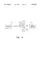
- apparatus 26 for controlling the printingincludes an PDMS support 28 upon which optical fiber 10 is placed, a mount 30, upon which support 28 is placed is controlled by a vertical translation stage 32, a rotation stage 34, and a horizontal translation stage 36. Above support 28 and optical fiber 10 is mounted article 18, with is contoured surface 20 facing the optical fiber.
- Article 18is carried by a mount 38 that is positioned by a rotational stage 40 and a horizontal translation stage 42.
- a laser beam 44that passes through the apparatus and is reflected ensures that the stages are properly aligned.
- a charge-coupled detector camera 46connected to a microscope 48 and a video display allows observation of the printing to ensure accuracy.
- FIG. 4an arrangement for optically writing an in-fiber grating in optical fiber 10 is illustrated.
- photomask 12is printed on the exterior surface of optical fiber 10 so as to extend about the entire circumference of the optical fiber
- the optical fibercan be exposed to radiation about its entire circumference, and such an arrangement is illustrated in FIG. 4.
- Light sources 50, 52, 54, and 56are positioned at relative orientations 0°, 90°, 180° and 270° about the optical fiber and the fiber is irradiated from these four evenly-spaced radial directions, for purposes of illustration. As discussed above, however, any orientation of radiation can be used.
- the optical fibercan include, for the purpose of monitoring the progress of creation of a diffraction grating in the fiber, at one end a broadband light source 58, and at another end an optical spectrum analyzer 60.
- the broadband sourceis passed through the fiber during irradiation from sources 50, 52, 54, and 56 to write the diffraction grating in the fiber and the optical spectrum analyzer determines a change in transmission spectrum of the fiber as a function of time of irradiation.
- a wavelength of light from the broadband source that resonates at the grating periodicitywill exhibit a significant drop in transmission.
- the extent of radiation requiredcan be determined in this manner. That is, an indication of when the grating has been written effectively is given.
- Photomask 12Described is a technique for forming an amplitude-modulating agent (photomask 12) on an exterior surface of an optical fiber. Photomask 12 also can be formed in other techniques described below in connection with fabrication of small-scale structures on cylindrical substrates.
- amplitude-modulating pattern 12need not be formed on optical fiber 10, but can be formed in the surface of optical fiber 10 by etching bands in optical fiber 10 corresponding to regions 14 followed by application within the etched, cylindrical grooves of an amplitude-modulating agent.
- amplitude-modulating pattern 12is a radiation-altering pattern that alters radiation to which optical fiber 10 is exposed to selectively change refractive indices of portions 16 to an extent greater than portions 14. Pattern 12 modulates the radiation completely by completely blocking radiation from portions 14 of the fiber core, or by partially blocking such radiation from the core.
- optical fiber 10(or other article) includes material at its surface that is absorptive or reflective of radiation selected to induce a change in refractive index in the article.
- This materialis selectively removed to form the amplitude-modulating pattern by, for example, using article 18 to print bands of a precursor on the fiber, the precursor dictating the pattern of removal of the outer material.
- a self-assembled monolayercan be applied that is resistant to an etchant which removes the material, and following exposure of this arrangement to the etchant and optional removal of the self-assembled monolayer, the amplitude-modulating pattern is present at the surface in a pattern corresponding to the self-assembled monolayer pattern.
- the self-assembled monolayercan direct a resist precursor to regions uncoated by the self-assembled monolayer, and, following etching, a pattern complementary to the original pattern of the self-assembled monolayer will exist as an amplitude-modulating pattern.
- the radiation-altering patternis a phase-modulating pattern applied to the surface of an article such as optical fiber 10 or created in the surface of the article.
- the phase-modulating patternlike the amplitude-modulating pattern such as photomask 12, adheres to optical fiber 10 to the extent that it translates with any vibrations, as described above. That is, it is integral with optical fiber 10 to that extent.
- a phase-modulating patterncan be created as described above in connection with the amplitude-modulating pattern, using similar techniques and similar materials, or according to any of the techniques described below, or as described in U.S. Pat. No. 5,512,131. The particular technique can be selected by those of ordinary skill in the art for convenience.
- a phase-modulating patternwill serve as a phase grating that, when optical fiber 10 is irradiated, will create alternating regions of constructive and destructive interference at the fiber core that will cause first portions of the fiber core to undergo a change in refractive index to an extent greater than second, contiguous, interspersed portions.
- the phase-modulating patternallows for exposure of the optical fiber to radiation at any or all locations circumferentially.
- the phase-modulating patternneed not be applied or created in the fiber throughout the entire circumference, but only to the extent that the fiber will be exposed to radiation.
- the phase-modulating patternneed not involve a separate agent, but can involve etching bands within the surface of an article such as optical fiber 10 without application of any auxiliary agent. Exposure of such a fiber to electromagnetic radiation will result in creation of a diffraction pattern of light directed at the fiber core, resulting in a pattern of differing indices of refraction in the core. Dimensions associated with a phase-modulating pattern can be selected by one of ordinary skill in the art with knowledge of the dimensions of the jacket, cladding, and core of optical fiber 10. In the phase-modulating embodiment, the phase-modulating pattern at the surface of fiber 10 generally will not correspond to the pattern of alternating indices of refraction created in the fiber core.
- Gratings written in optical fibersserve a variety of uses, as is known to those of ordinary skill in art. Wavelength selection, tunability, mode selectivity and noise suppression are exemplary uses.
- an optical fiber containing an in-fiber gratingcan define a sensor, for example a strain or temperature sensor. As strain is applied to the fiber, or the temperature of the fiber changes, the wavelength of light resonant with the grating will change.
- Gratingsalso can be used for in-fiber lasers to create cavity feedback.
- a filter/reflectorcan be made by establishing a resonant cavity bounded by in-fiber gratings that passes only selected wavelengths.
- the inventionalso provides techniques for fabricating small-scale metallic structures such as coils and stents, optionally on the exterior surface of cylindrical articles.
- a cylindrical article 62(including, as illustrated, a hollow, central passageway 64) has an exterior surface 66 that is coated with a thin layer 68 of metal having an exterior surface 69.
- a pattern of a molecular speciesis formed on exterior surface 69, the pattern being the same as, or complementary to, a pattern 70 of metal layer 68 desirably retained on external surface 66 of article 62.
- the molecular speciescan be a self-assembled monolayer in coil pattern 70, which is resistant to an etchant that can remove metal 68.
- the molecular speciescan be a catalyst that promotes deposition of a metal from an electroless plating bath, and a plated metal protecting species, in the pattern of coil 70, applied to layer 68 in this manner. Subsequent etching can result in coil 70.
- a molecular speciescan be patterned in a pattern complementary to coil 70, which molecular species directs an etchant resist to form a pattern that covers coil pattern 70.
- the molecular specieswould be selected to be incompatible with a precursor of an etchant resist, where the precursor is more compatible with metal 68.
- the systemcan be exposed to an etch removing portions of metal layer 68 other than portions in a coil pattern 70.
- the metalcan be deposited via electroless deposition where metal pattern 70 is a catalyst, or by addressing metal coil 70 electrically and carrying out electrochemical deposition.
- the metal defined in coil pattern 70 and metal that is deposited thereon to define coil 72can be the same, or different, depending upon the fabrication technique.
- Metal coil 72 on substrate 62can serve a variety of purposes. According to one, passageway 64 receives an NMR sample and coil 72 serves as an electromagnet for NMR analysis. According to another, coil 72 is removed from substrate 62 by, for example, dissolving the substrate, and the coil is used as an NMR coil or other device. According to another embodiment, as illustrated in FIG. 5, coil 72 remains on substrate 62 and ferromagnetic material 74 is passed through central cavity 64 of substrate 62. Ferromagnetic material 74 passing through coil 72 defines a concentrically wound, cylindrical microtransformer.
- a multi-layer coiled arrangementis produced.
- the term "layer" of a coilmeans a coil that includes a metallic conductor in a coiled pattern where each portion of the conductor is in alignment, axially, with other portions of the coil. That is, a "layer” of a coil does not include conductor defining the coil on top of other conductor, or conductor sections staggered so that more “windings” can be provided per unit axial length of the coil.
- Each winding of the coilneed not have the same radius of curvature, as substrate 62 could taper, and a coil formed about substrate 62 when it is tapered would still involve a single "layer” of coil.
- the inventionprovides a coil having a layer of turns of at least 30 turns per mm, preferably at least about 50 turns per mm, and more preferably at least about 100 turns per mm.
- a second "layer" of coilis provided by inserting coil 72 and substrate 62 within a receptacle (central hollow portion) 76 of a cylindrical substrate 78 having deposited thereon a second coil 80.
- a concentric, cylindrical microtransformerresults. Both inner coil 72 and outer coil 80 can be contacted electrically.
- FIG. 6a technique for patterning a coil on an exterior surface of a cylindrical article is illustrated schematically.
- An article 18(as described above with reference to FIG. 2) is provided.
- An arrangement as described above with reference to FIG. 3can be used.
- a cylindrical article 82is placed on the top surfaces of protrusions 22 at an angle that is not perpendicular to the protrusions, and rolled across the protrusions.
- the relative orientation of the article and cylindrical article 82can be adjusted so that when the cylindrical article 82 is rolled across the surface of the article 18 a continuous coil is printed on the exterior surface of cylindrical article 82.
- the material printed on the exterior surface of article 82thereby can prevent removal of material from the surface or initiate deposition of the material at the surface.
- ⁇is the angle made between linear protrusions 22 and a line perpendicular to the axis of article 82
- dis the dimension of the spacing of the protrusions
- ris the radius of cylindrical article 82
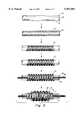
- the techniqueinvolves providing a cylindrical article 84 having an exterior surface 86, depositing a thin layer of metal on surface 87, and removing a first portion of the layer of metal from the substrate while allowing a second, discontinuous, interconnected portion of the metal layer 88 to remain on the substrate.
- discontinuous, interconnected portionis meant to define a portion of a layer of metal that includes voids, but is interconnected in that electrical contact with any portion of the portion provides electrical contact with the entire portion.
- a coilis a discontinuous, interconnected portion of a layer of metal.
- Removal of portions of metal layer 87can be carried out by etching the first portions of the metal layer. This can be done by protecting second portion 88 by microcontact printing (U.S. Pat. No. 5,512,131) a pattern of a protecting species corresponding to portion 88 on layer 87. This can be accomplished by providing an article (not shown) similar to article 18 but including a protrusion pattern corresponding to the pattern of portion 88 of the metal layer, coating the protrusions with a precursor of an etchant resist, and forming the resist at portions 88 by rolling article 84 across the article, thereby transferring to portion 88 the precursor of the etchant resist.
- the precursor of the etchant resistcan be a self-assembled monolayer-forming species, thus the etchant resist at portions 88 can be a self-assembled monolayer.
- a self-assembled monolayercan be formed at portion 88, followed by exposure of the arrangement to an etchant resist that is chemically compatible with the self-assembled monolayer at portion 88.
- a hydrophobic etchant resistwill readily be applied to the self-assembled monolayer and serve as an etchant resist.
- a layer of metal that defines the stentis deposited on the patterned, second portion 88.
- a discontinuous, interconnected, cylindrical, metallic article 90having a thickness suitable for removal from substrate 84 to serve as a free-standing article, results.
- Deposition of metal at second portion pattern 88can be carried out according to a variety of methods. According to one, portion 88 is a catalyst and the article is subjected to electroless deposition. According to another, electrical connection is made with pattern 88 and metal is electrochemically deposited at portion 88. Both techniques are well-known to those with ordinary skill in the art.
- article 90is removed from substrate 84 by, for example, dissolving substrate 84.
- a resulting free-standing article 90results.
- article 90serves as a stent, it can be disposed about an inflatable balloon of a catheter, positioned in a desired region of a vessel (typically a coronary artery) and expanded against the vessel wall by inflation of the balloon.
- the discontinuous pattern of article 90can be expanded since portions of the pattern that run axially will, when the stent is expanded, be drawn into a zig-zag pattern (this can be visualized more easily with reference to structure 88).
- an alternate pattern for patterned metal portion 88is illustrated. This pattern can be arranged about the cylindrical article with the axis of the article lying in any orientation relative to the pattern of FIG. 8, and the resulting stent is easily expandable.
- techniques for creation of one arrangementcan be used for creation of any other arrangement.
- the inventionlies in the technique of printing, on a surface of an article, a precursor that dictates a pattern of deposition on the article, etching in the article, or a combination for creation of a variety of useful devices.
- the patterncan be formed on or in a cylindrical article and, according to one embodiment, involves a pattern having at least one continuous, isolated portion that encircles the cylinder.
- continuous, isolated portion that encircles the cylinderis meant to define an arcuate portion that encircles the cylinder at least once, for example, as defining a cylindrical band or one period of a coil, and is isolated in that the portion circling the article does not contact other portions except where it contacts itself as in a band.
- Polyimide-coated capillarieswere obtained from Polymicro Technologies, Inc. (Phoenix, Ariz.). The polyimide coating was burned off using a resistively-heated filament. The outer diameter of the stripped fiber was 134.5 ⁇ 0.5 microns, and the inner diameter was 95.6 ⁇ 1.5 microns. The stripped capillaries were coated with titanium (about 15-30 Angstroms) and silver (about 300-500 Angstroms) using an electron beam evaporator. Mechanical stages were used to rotate the capillaries about two orthogonal axes during deposition.
- Lines of a self-assembled monolayer formed of hexadecanethiolwere printed on the outside of the capillaries using an arrangement as illustrated in FIG. 6.
- the self-assembled monolayerwas printed in a pattern complementary to that of metal pattern 70 as illustrated in FIG. 5.
- the hexadecanethiol-printed capillarieswere inserted into a ferri/ferrocyanide bath to remove silver not protected by the hexadecanethiol according to pattern 70 as illustrated in FIG. 5. Etching times on the order of 20 seconds were sufficient. This resulted in silver spirals 70 of a few hundred Angstroms thickness on glass capillaries coated with titanium a few tens of Angstroms thick.
- the sampleswere exposed 1% hydrofluoric acid for ten seconds to remove the exposed titanium.
- a thin, gold wirewas attached to one end of the silver-titanium spiral 70 using silver paint. Gold then was electroplated onto metallic pattern 70 by adjusting the current density to about 4 mA/cm 2 and plating for several minutes. The plating technique resulted in spirals 72 made of gold, approximately 1-3 microns thick, on top of silver on top of titanium adhered to the outside of glass capillary 62.
- the spiral 72can be used as an electromagnet in, for example, an NMR arrangement in which an NMR sample is passed through the central portion 64 of the capillary 62.
- Coils 72 having a lateral dimension (dimension of a portion of the coil, in a direction axially, of 150, 50 and 20 microns) coils of lengthwere produced.
- a micro-NMR sample tubewas fabricated.
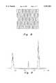
- a silver-titanium spiral 70 of 1 turn per 100 microns length, 17 turns in lengthwas formed on the outside of a stripped capillary as described in Example 1. Subsequently, copper was plated on the silver-titanium coil.
- Neat ethylbenzene(including a small amount of water contaminant) was introduced into the capillary. NMR analysis was carried out as described in Olson, et al., Science, 270, 1967-1970 (Dec. 22, 1995). The sample, coil, and tube were immersed in fluorinertTM FC-43 and placed in a General Electric GN-300WB 300 MHz sperometer, and an NMR spectrum obtained.WTM The spectrum appears in FIG. 9.
- Ferromagnetic wire(80% Ni, 15% Fe, 4.4% Mo, 6.6% other; diameter of 80 ⁇ 2 microns) was inserted into the core of the capillary (opening 64).
- the wireis sold under the mark MONIFE 479 from California Fine Wire (Grover Beach, Calif.).
- the outer coilwas contacted electrically.
- the connectionswere made with a test fixture of an LCR meter (Hewlett-Packard model 4284 A with internal DC bias, option 001) and Test Fixture 16334 A SMD. With this meter, inductance and resistance were determined as a function of frequency, magnitude of current used for the test, and magnitude of a constant bias applied during the test period.
- a second arrangementinvolved a second coil spaced from the first coil. Electrical connection was made to each coil. Using two coils around adjacent regions of the same capillary, qualitative measurement of magnetic field induced by an alternating current passing through one of the coils was made by measuring the induced voltage in the other coil. For a given number of turns per inch, the inductance was a linear function of the length of the coil, and inductance per unit length was a quadratic function of the number of turns per unit length. The resulting electromagnet can be treated as an ideal solenoid, and the saturation point of the core material is the only limiting factor in the achievable magnetic field.
- a structure including an inner coil, an outer coil, and a central wirewas fabricated as described above in connection with Examples 1 and 3 and as illustrated in FIG. 5.
- the coupling efficiency in the frequency range from 1 kHz to 1 MHzwas calculated.
- the microtransformerhad efficient coupling (coupling efficiency greater than 0.9) of its primary and secondary coils at frequencies less than 20 kHz.
Landscapes
- Engineering & Computer Science (AREA)
- Physics & Mathematics (AREA)
- General Physics & Mathematics (AREA)
- Chemical & Material Sciences (AREA)
- Manufacturing & Machinery (AREA)
- Nanotechnology (AREA)
- Power Engineering (AREA)
- Condensed Matter Physics & Semiconductors (AREA)
- Optics & Photonics (AREA)
- Crystallography & Structural Chemistry (AREA)
- Composite Materials (AREA)
- Materials Engineering (AREA)
- Diffracting Gratings Or Hologram Optical Elements (AREA)
Abstract
Description
Claims (28)
Priority Applications (7)
| Application Number | Priority Date | Filing Date | Title |
|---|---|---|---|
| US08/681,235US5951881A (en) | 1996-07-22 | 1996-07-22 | Fabrication of small-scale cylindrical articles |
| DE69727667TDE69727667T2 (en) | 1996-05-09 | 1997-05-09 | MANUFACTURE OF SMALL COILS AND TAPES AS A PHOTOMASK ON OPTICAL FAIRS FOR THE PRODUCTION OF FIBER EMITTERS, ELECTROMAGNETS AS MICRO-NMR COILS, MICRO-TRANSFORMERS AND INTRAVSCULAR STANTS |
| EP97936931AEP0900398B1 (en) | 1996-05-09 | 1997-05-09 | Fabrication of small-scale coils and bands as photomasks on optical fibers for generation of in-fiber gratings, electromagnets as micro-nmr coils, microtransformers, and intra-vascular stents |
| AU39571/97AAU3957197A (en) | 1996-05-09 | 1997-05-09 | Fabrication of small-scale coils and bands as photomasks on optical fibers for generation of in-fiber gratings, electromagnets as micro-nmr coils, microtransformers, and intra-vascular stents |
| PCT/US1997/008144WO1997044692A2 (en) | 1996-05-09 | 1997-05-09 | Fabrication of small-scale coils and bands as photomasks on optical fibers for generation of in-fiber gratings, electromagnets as micro-nmr coils, microtransformers, and intra-vascular stents |
| JP09542509AJP2000515477A (en) | 1996-05-09 | 1997-05-09 | Manufacture of micro-coils and strips as photomasks on optical fibers for the production of micro-NMR coils, micro-transformers, intra-fiber gratings as endovascular stents, electromagnets |
| AT97936931TATE259966T1 (en) | 1996-05-09 | 1997-05-09 | PRODUCTION OF SMALL COILS AND TAPES AS PHOTOMASKS ON OPTICAL FIBERS FOR GENERATING FIBER EMMITTERS, ELECTROMAGNETS AS MICRO-NMR COILS, MICROTRANSFORMERS AND INTRAVSCULAR STANTS |
Applications Claiming Priority (1)
| Application Number | Priority Date | Filing Date | Title |
|---|---|---|---|
| US08/681,235US5951881A (en) | 1996-07-22 | 1996-07-22 | Fabrication of small-scale cylindrical articles |
Publications (1)
| Publication Number | Publication Date |
|---|---|
| US5951881Atrue US5951881A (en) | 1999-09-14 |
Family
ID=24734386
Family Applications (1)
| Application Number | Title | Priority Date | Filing Date |
|---|---|---|---|
| US08/681,235Expired - LifetimeUS5951881A (en) | 1996-05-09 | 1996-07-22 | Fabrication of small-scale cylindrical articles |
Country Status (1)
| Country | Link |
|---|---|
| US (1) | US5951881A (en) |
Cited By (135)
| Publication number | Priority date | Publication date | Assignee | Title |
|---|---|---|---|---|
| US6180239B1 (en) | 1993-10-04 | 2001-01-30 | President And Fellows Of Harvard College | Microcontact printing on surfaces and derivative articles |
| US6229941B1 (en)* | 1998-10-07 | 2001-05-08 | Samsung Electronics Co., Ltd. | Apparatus and method of fabricating long-period fiber grating |
| US6275631B1 (en) | 1998-10-13 | 2001-08-14 | Samsung Electronics Co., Ltd. | Apparatus for manufacturing long-period optical fiber grating |
| US6379383B1 (en) | 1999-11-19 | 2002-04-30 | Advanced Bio Prosthetic Surfaces, Ltd. | Endoluminal device exhibiting improved endothelialization and method of manufacture thereof |
| US6509100B1 (en) | 1999-08-18 | 2003-01-21 | The University Of Houston System | Fluorinated hydrogn bond stabilized surface modifying agents, articles made therefrom, methods for making and using the same |
| US20030028246A1 (en)* | 1999-11-19 | 2003-02-06 | Palmaz Julio C. | Compliant implantable medical devices and methods of making same |
| US6518168B1 (en)* | 1995-08-18 | 2003-02-11 | President And Fellows Of Harvard College | Self-assembled monolayer directed patterning of surfaces |
| US6537310B1 (en) | 1999-11-19 | 2003-03-25 | Advanced Bio Prosthetic Surfaces, Ltd. | Endoluminal implantable devices and method of making same |
| US6558733B1 (en) | 2000-10-26 | 2003-05-06 | Advanced Cardiovascular Systems, Inc. | Method for etching a micropatterned microdepot prosthesis |
| US6563080B2 (en)* | 2001-02-15 | 2003-05-13 | Scimed Life Systems, Inc. | Laser cutting of stents and other medical devices |
| US6576406B1 (en)* | 2000-06-29 | 2003-06-10 | Sarcos Investments Lc | Micro-lithographic method and apparatus using three-dimensional mask |
| US6576000B2 (en)* | 2001-03-06 | 2003-06-10 | Scimed Life Systems, Inc. | Devices and methods for tissue repair |
| US20030163187A1 (en)* | 2002-02-25 | 2003-08-28 | Jan Weber | Non-invasive heating of implanted vascular treatment device |
| US20030177450A1 (en)* | 2002-03-12 | 2003-09-18 | Alex Nugent | Physical neural network design incorporating nanotechnology |
| US6695865B2 (en) | 2000-03-20 | 2004-02-24 | Advanced Bio Prosthetic Surfaces, Ltd. | Embolic protection device |
| US20040039717A1 (en)* | 2002-08-22 | 2004-02-26 | Alex Nugent | High-density synapse chip using nanoparticles |
| US20040054349A1 (en)* | 2002-09-12 | 2004-03-18 | Jerry Brightbill | Reinforced catheter and methods of making |
| US20040070893A1 (en)* | 1999-12-10 | 2004-04-15 | Ahn Kie Y. | Microtransformer for system-on-chip power supply |
| US6733513B2 (en) | 1999-11-04 | 2004-05-11 | Advanced Bioprosthetic Surfaces, Ltd. | Balloon catheter having metal balloon and method of making same |
| US20040114848A1 (en)* | 2002-09-06 | 2004-06-17 | Anbo Wang | Intrinsic Fabry-Perot optical fiber sensors and their multiplexing |
| US6764505B1 (en) | 2001-04-12 | 2004-07-20 | Advanced Cardiovascular Systems, Inc. | Variable surface area stent |
| US20040153426A1 (en)* | 2002-03-12 | 2004-08-05 | Alex Nugent | Physical neural network liquid state machine utilizing nanotechnology |
| US20040162796A1 (en)* | 2002-03-12 | 2004-08-19 | Alex Nugent | Application of Hebbian and anti-Hebbian learning to nanotechnology-based physical neural networks |
| US20040166140A1 (en)* | 1996-07-02 | 2004-08-26 | Santini John T. | Implantable device for controlled release of drug |
| US6834201B2 (en) | 2001-01-29 | 2004-12-21 | Stereotaxis, Inc. | Catheter navigation within an MR imaging device |
| US20040260315A1 (en)* | 2003-06-17 | 2004-12-23 | Dell Jeffrey R. | Expandable tissue support member and method of forming the support member |
| US20040260391A1 (en)* | 1999-11-17 | 2004-12-23 | Santini John T. | Stent for controlled release of drug |
| US20050015351A1 (en)* | 2003-07-18 | 2005-01-20 | Alex Nugent | Nanotechnology neural network methods and systems |
| US6849085B2 (en) | 1999-11-19 | 2005-02-01 | Advanced Bio Prosthetic Surfaces, Ltd. | Self-supporting laminated films, structural materials and medical devices manufactured therefrom and method of making same |
| US20050033411A1 (en)* | 2000-09-28 | 2005-02-10 | Wu Steven Z. | Surface features of an implantable medical device |
| US20050105225A1 (en)* | 2003-08-06 | 2005-05-19 | Micron Technology, Inc. | Microtransformer for system-on-chip power supply |
| US20050112873A1 (en)* | 2002-02-26 | 2005-05-26 | Zangmeister Christopher D. | Method for selective electroless attachment of contacts to electrochemically-active molecules |
| US20050131521A1 (en)* | 2000-05-12 | 2005-06-16 | Denes Marton | Self-supporting laminated films, structural materials and medical devices manufactured therefrom and methods of making same |
| US20060052865A1 (en)* | 2004-09-09 | 2006-03-09 | Banas Christopher E | Stents with metallic covers and methods of making same |
| US20060100608A1 (en)* | 2002-08-16 | 2006-05-11 | Uhland Scott A | Controlled release device and method using electrothermal ablation |
| US7077860B2 (en) | 1997-04-24 | 2006-07-18 | Advanced Cardiovascular Systems, Inc. | Method of reducing or eliminating thrombus formation |
| US20060184466A1 (en)* | 2005-01-31 | 2006-08-17 | Alex Nugent | Fractal memory and computational methods and systems based on nanotechnology |
| US20060189963A1 (en)* | 1999-12-10 | 2006-08-24 | Massachusetts Institute Of Technology | Multi-reservoir device for controlled drug delivery |
| US20070005532A1 (en)* | 2005-05-23 | 2007-01-04 | Alex Nugent | Plasticity-induced self organizing nanotechnology for the extraction of independent components from a data stream |
| US7169173B2 (en) | 2001-06-29 | 2007-01-30 | Advanced Cardiovascular Systems, Inc. | Composite stent with regioselective material and a method of forming the same |
| US7195641B2 (en) | 1999-11-19 | 2007-03-27 | Advanced Bio Prosthetic Surfaces, Ltd. | Valvular prostheses having metal or pseudometallic construction and methods of manufacture |
| US7198675B2 (en) | 2003-09-30 | 2007-04-03 | Advanced Cardiovascular Systems | Stent mandrel fixture and method for selectively coating surfaces of a stent |
| US7235092B2 (en) | 1999-11-19 | 2007-06-26 | Advanced Bio Prosthetic Surfaces, Ltd. | Guidewires and thin film catheter-sheaths and method of making same |
| US20070152669A1 (en)* | 2005-12-29 | 2007-07-05 | Intel Corporation | Integrated on-chip nmr and esr device and method for making and using the same |
| US20070176643A1 (en)* | 2005-06-17 | 2007-08-02 | Alex Nugent | Universal logic gate utilizing nanotechnology |
| US7258891B2 (en) | 2001-06-28 | 2007-08-21 | Advanced Cardiovascular Systems, Inc. | Stent mounting assembly and a method of using the same to coat a stent |
| US7297159B2 (en) | 2000-10-26 | 2007-11-20 | Advanced Cardiovascular Systems, Inc. | Selective coating of medical devices |
| US7300457B2 (en) | 1999-11-19 | 2007-11-27 | Advanced Bio Prosthetic Surfaces, Ltd. | Self-supporting metallic implantable grafts, compliant implantable medical devices and methods of making same |
| US20070275035A1 (en)* | 2006-05-24 | 2007-11-29 | Microchips, Inc. | Minimally Invasive Medical Implant Devices for Controlled Drug Delivery |
| US7398259B2 (en) | 2002-03-12 | 2008-07-08 | Knowmtech, Llc | Training of a physical neural network |
| US20080190889A1 (en)* | 2005-03-11 | 2008-08-14 | Industrial Technology Research Institute | Roller with microstructure and the manufactruing method thereof |
| US7445766B2 (en) | 2000-03-02 | 2008-11-04 | Microchips, Inc. | Medical device and method for diagnostic sensing |
| US7476523B2 (en) | 2000-08-14 | 2009-01-13 | Surface Logix, Inc. | Method of patterning a surface using a deformable stamp |
| US20090043722A1 (en)* | 2003-03-27 | 2009-02-12 | Alex Nugent | Adaptive neural network utilizing nanotechnology-based components |
| US7553377B1 (en) | 2004-04-27 | 2009-06-30 | Advanced Cardiovascular Systems, Inc. | Apparatus and method for electrostatic coating of an abluminal stent surface |
| US20090169147A1 (en)* | 2004-02-12 | 2009-07-02 | Ellwood Jr Sutherland C | Apparatus, method, and computer program product for integrated influencer element |
| US7563324B1 (en) | 2003-12-29 | 2009-07-21 | Advanced Cardiovascular Systems Inc. | System and method for coating an implantable medical device |
| US20090228415A1 (en)* | 2002-06-05 | 2009-09-10 | Alex Nugent | Multilayer training in a physical neural network formed utilizing nanotechnology |
| US20090228416A1 (en)* | 2002-08-22 | 2009-09-10 | Alex Nugent | High density synapse chip using nanoparticles |
| US7599895B2 (en) | 2005-07-07 | 2009-10-06 | Knowm Tech, Llc | Methodology for the configuration and repair of unreliable switching elements |
| US7632307B2 (en) | 2004-12-16 | 2009-12-15 | Advanced Cardiovascular Systems, Inc. | Abluminal, multilayer coating constructs for drug-delivery stents |
| US20090311629A1 (en)* | 2008-06-12 | 2009-12-17 | National Cheng Kung University | Method for manufacturing roller mold |
| US7704274B2 (en) | 2002-09-26 | 2010-04-27 | Advanced Bio Prothestic Surfaces, Ltd. | Implantable graft and methods of making same |
| US7736687B2 (en) | 2006-01-31 | 2010-06-15 | Advance Bio Prosthetic Surfaces, Ltd. | Methods of making medical devices |
| US7862495B2 (en) | 2001-05-31 | 2011-01-04 | Advanced Cardiovascular Systems, Inc. | Radiation or drug delivery source with activity gradient to minimize edge effects |
| US7867547B2 (en) | 2005-12-19 | 2011-01-11 | Advanced Cardiovascular Systems, Inc. | Selectively coating luminal surfaces of stents |
| US7930257B2 (en) | 2007-01-05 | 2011-04-19 | Knowm Tech, Llc | Hierarchical temporal memory utilizing nanotechnology |
| US7931683B2 (en) | 2007-07-27 | 2011-04-26 | Boston Scientific Scimed, Inc. | Articles having ceramic coated surfaces |
| US7938855B2 (en) | 2007-11-02 | 2011-05-10 | Boston Scientific Scimed, Inc. | Deformable underlayer for stent |
| US7942926B2 (en) | 2007-07-11 | 2011-05-17 | Boston Scientific Scimed, Inc. | Endoprosthesis coating |
| US7976915B2 (en) | 2007-05-23 | 2011-07-12 | Boston Scientific Scimed, Inc. | Endoprosthesis with select ceramic morphology |
| US7981150B2 (en) | 2006-11-09 | 2011-07-19 | Boston Scientific Scimed, Inc. | Endoprosthesis with coatings |
| US7985252B2 (en) | 2008-07-30 | 2011-07-26 | Boston Scientific Scimed, Inc. | Bioerodible endoprosthesis |
| US7998192B2 (en) | 2008-05-09 | 2011-08-16 | Boston Scientific Scimed, Inc. | Endoprostheses |
| US8002823B2 (en) | 2007-07-11 | 2011-08-23 | Boston Scientific Scimed, Inc. | Endoprosthesis coating |
| US8003156B2 (en) | 2006-05-04 | 2011-08-23 | Advanced Cardiovascular Systems, Inc. | Rotatable support elements for stents |
| US8002821B2 (en) | 2006-09-18 | 2011-08-23 | Boston Scientific Scimed, Inc. | Bioerodible metallic ENDOPROSTHESES |
| US8017237B2 (en) | 2006-06-23 | 2011-09-13 | Abbott Cardiovascular Systems, Inc. | Nanoshells on polymers |
| US8029554B2 (en) | 2007-11-02 | 2011-10-04 | Boston Scientific Scimed, Inc. | Stent with embedded material |
| US8048448B2 (en) | 2006-06-15 | 2011-11-01 | Abbott Cardiovascular Systems Inc. | Nanoshells for drug delivery |
| US8048150B2 (en) | 2006-04-12 | 2011-11-01 | Boston Scientific Scimed, Inc. | Endoprosthesis having a fiber meshwork disposed thereon |
| US8048441B2 (en) | 2007-06-25 | 2011-11-01 | Abbott Cardiovascular Systems, Inc. | Nanobead releasing medical devices |
| US8052745B2 (en) | 2007-09-13 | 2011-11-08 | Boston Scientific Scimed, Inc. | Endoprosthesis |
| US8052744B2 (en) | 2006-09-15 | 2011-11-08 | Boston Scientific Scimed, Inc. | Medical devices and methods of making the same |
| US8052743B2 (en) | 2006-08-02 | 2011-11-08 | Boston Scientific Scimed, Inc. | Endoprosthesis with three-dimensional disintegration control |
| US8057534B2 (en) | 2006-09-15 | 2011-11-15 | Boston Scientific Scimed, Inc. | Bioerodible endoprostheses and methods of making the same |
| US8066763B2 (en) | 1998-04-11 | 2011-11-29 | Boston Scientific Scimed, Inc. | Drug-releasing stent with ceramic-containing layer |
| US8067054B2 (en) | 2007-04-05 | 2011-11-29 | Boston Scientific Scimed, Inc. | Stents with ceramic drug reservoir layer and methods of making and using the same |
| US8070797B2 (en) | 2007-03-01 | 2011-12-06 | Boston Scientific Scimed, Inc. | Medical device with a porous surface for delivery of a therapeutic agent |
| US8071156B2 (en) | 2009-03-04 | 2011-12-06 | Boston Scientific Scimed, Inc. | Endoprostheses |
| US8080055B2 (en) | 2006-12-28 | 2011-12-20 | Boston Scientific Scimed, Inc. | Bioerodible endoprostheses and methods of making the same |
| US8089029B2 (en) | 2006-02-01 | 2012-01-03 | Boston Scientific Scimed, Inc. | Bioabsorbable metal medical device and method of manufacture |
| US8128689B2 (en) | 2006-09-15 | 2012-03-06 | Boston Scientific Scimed, Inc. | Bioerodible endoprosthesis with biostable inorganic layers |
| US8187620B2 (en) | 2006-03-27 | 2012-05-29 | Boston Scientific Scimed, Inc. | Medical devices comprising a porous metal oxide or metal material and a polymer coating for delivering therapeutic agents |
| US8216632B2 (en) | 2007-11-02 | 2012-07-10 | Boston Scientific Scimed, Inc. | Endoprosthesis coating |
| US8221822B2 (en) | 2007-07-31 | 2012-07-17 | Boston Scientific Scimed, Inc. | Medical device coating by laser cladding |
| US8231980B2 (en) | 2008-12-03 | 2012-07-31 | Boston Scientific Scimed, Inc. | Medical implants including iridium oxide |
| US8236046B2 (en) | 2008-06-10 | 2012-08-07 | Boston Scientific Scimed, Inc. | Bioerodible endoprosthesis |
| US8267992B2 (en) | 2009-03-02 | 2012-09-18 | Boston Scientific Scimed, Inc. | Self-buffering medical implants |
| US8287937B2 (en) | 2009-04-24 | 2012-10-16 | Boston Scientific Scimed, Inc. | Endoprosthese |
| US8303643B2 (en) | 2001-06-27 | 2012-11-06 | Remon Medical Technologies Ltd. | Method and device for electrochemical formation of therapeutic species in vivo |
| US8313523B2 (en) | 2003-05-07 | 2012-11-20 | Advanced Bio Prosthetic Surfaces, Ltd. | Metallic implantable grafts and method of making same |
| US20120298617A1 (en)* | 2009-05-19 | 2012-11-29 | Korea University Research And Business Foundation | Apparatus for nano structure fabrication |
| US8353949B2 (en) | 2006-09-14 | 2013-01-15 | Boston Scientific Scimed, Inc. | Medical devices with drug-eluting coating |
| US8382824B2 (en) | 2008-10-03 | 2013-02-26 | Boston Scientific Scimed, Inc. | Medical implant having NANO-crystal grains with barrier layers of metal nitrides or fluorides |
| US20130057309A1 (en)* | 2010-02-12 | 2013-03-07 | Luzcom Inc. | Manufacturing method for contact for current inspection jig, contact for current inspection jig manufactured using said method, and current inspection jig provided with said contact |
| US8431149B2 (en) | 2007-03-01 | 2013-04-30 | Boston Scientific Scimed, Inc. | Coated medical devices for abluminal drug delivery |
| TWI394993B (en)* | 2009-11-03 | 2013-05-01 | Univ Nat Kaohsiung Applied Sci | Method for manufacturing a tunable long-period fiber grating |
| US8449603B2 (en) | 2008-06-18 | 2013-05-28 | Boston Scientific Scimed, Inc. | Endoprosthesis coating |
| US8458879B2 (en) | 2001-07-03 | 2013-06-11 | Advanced Bio Prosthetic Surfaces, Ltd., A Wholly Owned Subsidiary Of Palmaz Scientific, Inc. | Method of fabricating an implantable medical device |
| CN103153248A (en)* | 2010-07-20 | 2013-06-12 | 约翰霍普金斯大学 | Interferometric force sensor for surgical instruments |
| US8574615B2 (en) | 2006-03-24 | 2013-11-05 | Boston Scientific Scimed, Inc. | Medical devices having nanoporous coatings for controlled therapeutic agent delivery |
| US8603530B2 (en) | 2006-06-14 | 2013-12-10 | Abbott Cardiovascular Systems Inc. | Nanoshell therapy |
| US8641754B2 (en) | 2000-11-07 | 2014-02-04 | Advanced Bio Prosthetic Surfaces, Ltd. a wholly owned subsidiary of Palmaz Scientific, Inc. | Endoluminal stent, self-supporting endoluminal graft and methods of making same |
| US8668732B2 (en) | 2010-03-23 | 2014-03-11 | Boston Scientific Scimed, Inc. | Surface treated bioerodible metal endoprostheses |
| CN103811148A (en)* | 2012-11-09 | 2014-05-21 | 辉达公司 | Winding inductor for switching power supply and switching power supply with winding inductor |
| US8771343B2 (en) | 2006-06-29 | 2014-07-08 | Boston Scientific Scimed, Inc. | Medical devices with selective titanium oxide coatings |
| US8808726B2 (en) | 2006-09-15 | 2014-08-19 | Boston Scientific Scimed. Inc. | Bioerodible endoprostheses and methods of making the same |
| US8815273B2 (en) | 2007-07-27 | 2014-08-26 | Boston Scientific Scimed, Inc. | Drug eluting medical devices having porous layers |
| US8815275B2 (en) | 2006-06-28 | 2014-08-26 | Boston Scientific Scimed, Inc. | Coatings for medical devices comprising a therapeutic agent and a metallic material |
| US8840660B2 (en) | 2006-01-05 | 2014-09-23 | Boston Scientific Scimed, Inc. | Bioerodible endoprostheses and methods of making the same |
| US8900292B2 (en) | 2007-08-03 | 2014-12-02 | Boston Scientific Scimed, Inc. | Coating for medical device having increased surface area |
| US8920491B2 (en) | 2008-04-22 | 2014-12-30 | Boston Scientific Scimed, Inc. | Medical devices having a coating of inorganic material |
| US8932346B2 (en) | 2008-04-24 | 2015-01-13 | Boston Scientific Scimed, Inc. | Medical devices having inorganic particle layers |
| US9269043B2 (en) | 2002-03-12 | 2016-02-23 | Knowm Tech, Llc | Memristive neural processor utilizing anti-hebbian and hebbian technology |
| US9284409B2 (en) | 2007-07-19 | 2016-03-15 | Boston Scientific Scimed, Inc. | Endoprosthesis having a non-fouling surface |
| CN107180735A (en)* | 2016-03-11 | 2017-09-19 | 安捷伦科技有限公司 | Filament component and relevant devices, systems, and methods for producing electronics |
| US10172730B2 (en) | 1999-11-19 | 2019-01-08 | Vactronix Scientific, Llc | Stents with metallic covers and methods of making same |
| CN110115648A (en)* | 2019-05-15 | 2019-08-13 | 四川兴泰普乐医疗科技有限公司 | A kind of preparation method of 3D printing degradable blood vessel bracket |
| IT201900005362A1 (en)* | 2019-04-08 | 2020-10-08 | Centro Regionale Information Communication Tech Cerict Scarl | NEEDLE OR CATHETER PROVIDED WITH A PLURALITY OF OPTICAL FIBERS |
| US11660005B1 (en) | 2021-06-04 | 2023-05-30 | Huxley Medical, Inc. | Processing and analyzing biometric data |
| US11717221B1 (en) | 2020-03-11 | 2023-08-08 | Huxley Medical, Inc. | Patch for improved biometric data capture and related processes |
| US12109010B1 (en) | 2021-08-24 | 2024-10-08 | Huxley Medical, Inc. | Photoplethysmography sensors and processes |
| US12114980B1 (en) | 2021-08-24 | 2024-10-15 | Huxley Medical, Inc. | Photoplethysmography sensors and processes |
| US12178552B1 (en) | 2021-06-04 | 2024-12-31 | Huxley Medical, Inc. | Systems and processes for detecting oxygen saturation and compensating for skin tone variation |
Citations (19)
| Publication number | Priority date | Publication date | Assignee | Title |
|---|---|---|---|---|
| EP0140259A2 (en)* | 1983-11-02 | 1985-05-08 | General Electric Company | Transverse gradient field coil |
| US4528260A (en)* | 1983-04-27 | 1985-07-09 | Rca Corporation | Method of fabricating lenticular arrays |
| US4728591A (en)* | 1986-03-07 | 1988-03-01 | Trustees Of Boston University | Self-assembled nanometer lithographic masks and templates and method for parallel fabrication of nanometer scale multi-device structures |
| US4735890A (en)* | 1982-09-16 | 1988-04-05 | Tokyo Ohka Kogyo Kabushiki Kaisha | Photomasks for photolithographic fine patterning |
| US4802951A (en)* | 1986-03-07 | 1989-02-07 | Trustees Of Boston University | Method for parallel fabrication of nanometer scale multi-device structures |
| US4810621A (en)* | 1985-11-18 | 1989-03-07 | The Perkin-Elmer Corporation | Contact lithographic fabrication of patterns on large optics |
| US4897325A (en)* | 1985-11-18 | 1990-01-30 | The Perkin-Elmer Corporation | Contact lithographic fabrication of patterns on large optics |
| US4950568A (en)* | 1987-02-06 | 1990-08-21 | Johannes Heidenhain Gmbh | Radiation mask for the lithographic production of patterns |
| US5017960A (en)* | 1989-02-14 | 1991-05-21 | Std Engineering Ab | Exposure of radiation sensitive materials |
| US5018829A (en)* | 1984-11-19 | 1991-05-28 | Matsushita Electric Industrial Co., Ltd. | Optical fiber and method of producing the same |
| EP0441693A1 (en)* | 1990-02-06 | 1991-08-14 | Bertin & Cie | Method for making an index grating in an optical fibre, and quasi-distributed sensor network realized in this fibre |
| US5079600A (en)* | 1987-03-06 | 1992-01-07 | Schnur Joel M | High resolution patterning on solid substrates |
| JPH0473917A (en)* | 1990-07-16 | 1992-03-09 | Mitsubishi Electric Corp | Manufacture of inductance component |
| US5112438A (en)* | 1990-11-29 | 1992-05-12 | Hughes Aircraft Company | Photolithographic method for making helices for traveling wave tubes and other cylindrical objects |
| US5153084A (en)* | 1990-09-10 | 1992-10-06 | General Electric Company | Process for preparing a photo-mask for imaging three-dimensional objects |
| US5178976A (en)* | 1990-09-10 | 1993-01-12 | General Electric Company | Technique for preparing a photo-mask for imaging three-dimensional objects |
| US5421955A (en)* | 1991-10-28 | 1995-06-06 | Advanced Cardiovascular Systems, Inc. | Expandable stents and method for making same |
| US5512131A (en)* | 1993-10-04 | 1996-04-30 | President And Fellows Of Harvard College | Formation of microstamped patterns on surfaces and derivative articles |
| WO1997007429A1 (en)* | 1995-08-18 | 1997-02-27 | President And Fellows Of Harvard College | Self-assembled monolayer directed patterning of surfaces |
- 1996
- 1996-07-22USUS08/681,235patent/US5951881A/ennot_activeExpired - Lifetime
Patent Citations (20)
| Publication number | Priority date | Publication date | Assignee | Title |
|---|---|---|---|---|
| US4735890A (en)* | 1982-09-16 | 1988-04-05 | Tokyo Ohka Kogyo Kabushiki Kaisha | Photomasks for photolithographic fine patterning |
| US4528260A (en)* | 1983-04-27 | 1985-07-09 | Rca Corporation | Method of fabricating lenticular arrays |
| EP0140259A2 (en)* | 1983-11-02 | 1985-05-08 | General Electric Company | Transverse gradient field coil |
| US5018829A (en)* | 1984-11-19 | 1991-05-28 | Matsushita Electric Industrial Co., Ltd. | Optical fiber and method of producing the same |
| US4810621A (en)* | 1985-11-18 | 1989-03-07 | The Perkin-Elmer Corporation | Contact lithographic fabrication of patterns on large optics |
| US4897325A (en)* | 1985-11-18 | 1990-01-30 | The Perkin-Elmer Corporation | Contact lithographic fabrication of patterns on large optics |
| US4728591A (en)* | 1986-03-07 | 1988-03-01 | Trustees Of Boston University | Self-assembled nanometer lithographic masks and templates and method for parallel fabrication of nanometer scale multi-device structures |
| US4802951A (en)* | 1986-03-07 | 1989-02-07 | Trustees Of Boston University | Method for parallel fabrication of nanometer scale multi-device structures |
| US4950568A (en)* | 1987-02-06 | 1990-08-21 | Johannes Heidenhain Gmbh | Radiation mask for the lithographic production of patterns |
| US5079600A (en)* | 1987-03-06 | 1992-01-07 | Schnur Joel M | High resolution patterning on solid substrates |
| US5017960A (en)* | 1989-02-14 | 1991-05-21 | Std Engineering Ab | Exposure of radiation sensitive materials |
| EP0441693A1 (en)* | 1990-02-06 | 1991-08-14 | Bertin & Cie | Method for making an index grating in an optical fibre, and quasi-distributed sensor network realized in this fibre |
| JPH0473917A (en)* | 1990-07-16 | 1992-03-09 | Mitsubishi Electric Corp | Manufacture of inductance component |
| US5153084A (en)* | 1990-09-10 | 1992-10-06 | General Electric Company | Process for preparing a photo-mask for imaging three-dimensional objects |
| US5178976A (en)* | 1990-09-10 | 1993-01-12 | General Electric Company | Technique for preparing a photo-mask for imaging three-dimensional objects |
| US5112438A (en)* | 1990-11-29 | 1992-05-12 | Hughes Aircraft Company | Photolithographic method for making helices for traveling wave tubes and other cylindrical objects |
| US5421955A (en)* | 1991-10-28 | 1995-06-06 | Advanced Cardiovascular Systems, Inc. | Expandable stents and method for making same |
| US5421955B1 (en)* | 1991-10-28 | 1998-01-20 | Advanced Cardiovascular System | Expandable stents and method for making same |
| US5512131A (en)* | 1993-10-04 | 1996-04-30 | President And Fellows Of Harvard College | Formation of microstamped patterns on surfaces and derivative articles |
| WO1997007429A1 (en)* | 1995-08-18 | 1997-02-27 | President And Fellows Of Harvard College | Self-assembled monolayer directed patterning of surfaces |
Non-Patent Citations (32)
| Title |
|---|
| "Guide-Wave Control", Optical Integrated Circuits, pp. 96-137. |
| "Microfabrication Techniques in Optical Integrated Circuits", Optical Integrated Circuits, pp. 172-223. |
| "Plated Metal Mask for Precise Excimer Laser Ablation of Glasses", IBM Technical Disclosure Bulletin, vol. 34, No. 6, p. 253, Nov. 1991. |
| Ashish M. Vengsarkar, Paul J. Lemaire, Justin B. Judkins, Vikram Bhatia, Turan Erdogan and John E. Sipe, "Long-Period Fiber Gratings as Band-Rejection Filters", Journal of Lightwave Technology, vol. 14, No. 1, Jan. 1996, pp. 58-65. |
| Ashish M. Vengsarkar, Paul J. Lemaire, Justin B. Judkins, Vikram Bhatia, Turan Erdogan and John E. Sipe, Long Period Fiber Gratings as Band Rejection Filters , Journal of Lightwave Technology, vol. 14, No. 1, Jan. 1996, pp. 58 65.* |
| Dean L. Olson, Timothy L. Peck, Andrew G. Webb, Richard L. Magin and Jonathan V. Sweedler, "High-Resolution Microcoil 1 H-NMR for Mass-Limited, Nanoliter-Volume Samples", Science, vol. 270, Dec. 22, 1995, pp. 1967-1970. |
| Dean L. Olson, Timothy L. Peck, Andrew G. Webb, Richard L. Magin and Jonathan V. Sweedler, High Resolution Microcoil 1 H NMR for Mass Limited, Nanoliter Volume Samples , Science, vol. 270, Dec. 22, 1995, pp. 1967 1970.* |
| E.A. Dobisz et al., "Self-Assembled Monolayer Films for Nanofabrication", Mat. Res. Soc. Symp. Proc., vol. 380, 1995. |
| E.A. Dobisz et al., Self Assembled Monolayer Films for Nanofabrication , Mat. Res. Soc. Symp. Proc., vol. 380, 1995.* |
| Enoch, Kim et al. "Combining Patterned Self-Assembled Monolayers of Alkanethiolates on Gold with Anisotropic Etching of Silicon to Generate Controlled Surface Morphologies". J. Electrochem. Soc. vol. 142. No. 2. pp. 628-633 (Feb. 7, 1995). |
| Enoch, Kim et al. Combining Patterned Self Assembled Monolayers of Alkanethiolates on Gold with Anisotropic Etching of Silicon to Generate Controlled Surface Morphologies . J. Electrochem. Soc. vol. 142. No. 2. pp. 628 633 (Feb. 7, 1995).* |
| Guide Wave Control , Optical Integrated Circuits, pp. 96 137.* |
| HIll, K.O. et al., "Birefringent Photosensitivity in Monomode Optical Fibre; Application to External Writing of Rocking Filters", Electronics Letters, vol. 27, No. 17, pp. 1548-1550, Aug. 15, 1991. |
| HIll, K.O. et al., Birefringent Photosensitivity in Monomode Optical Fibre; Application to External Writing of Rocking Filters , Electronics Letters , vol. 27, No. 17, pp. 1548 1550, Aug. 15, 1991.* |
| J.K. Schoer et al., "Scanning Probe Lithography", Langmuir, vol. 10, No. 3, pp. 615-618, 1994. (Abstract Only). |
| J.K. Schoer et al., Scanning Probe Lithography , Langmuir, vol. 10, No. 3, pp. 615 618, 1994. (Abstract Only).* |
| Jacobsen et al. "Fabrication of Micro-Structures Using Non-Planar Lithography (NPL)" Proceedings. IEEE Micro Electro Mechanical Systems. An Investigation of Micro Structures. Sensors. Actuators. Machines and Robots. Nara. Japan. Jan. 30-Feb. 2, 1991. |
| Jacobsen et al. Fabrication of Micro Structures Using Non Planar Lithography (NPL) Proceedings. IEEE Micro Electro Mechanical Systems. An Investigation of Micro Structures. Sensors. Actuators. Machines and Robots. Nara. Japan. Jan. 30 Feb. 2, 1991.* |
| K.O. Hill, B. Malo, F. Bilodeau and D.C. Johnson, "Photosensitivy in Optical Fibers", Annu. Rev. Mater. Sci. 1993, 23:pp. 125-157. |
| K.O. Hill, B. Malo, F. Bilodeau and D.C. Johnson, Photosensitivy in Optical Fibers , Annu. Rev. Mater. Sci. 1993, 23:pp. 125 157.* |
| Microfabrication Techniques in Optical Integrated Circuits , Optical Integrated Circuits, pp. 172 223.* |
| Plated Metal Mask for Precise Excimer Laser Ablation of Glasses , IBM Technical Disclosure Bulletin , vol. 34, No. 6, p. 253, Nov. 1991.* |
| R. Kashyap et al., "UV written reflection grating structures in photosensitive optical fibres using phase-shifted phase marks", Electronics Letters, vol. 30, No, 23, pp. 1977-1978, Nov. 10, 1994. |
| R. Kashyap et al., UV written reflection grating structures in photosensitive optical fibres using phase shifted phase marks , Electronics Letters , vol. 30, No, 23, pp. 1977 1978, Nov. 10, 1994.* |
| Ron Dagani, "Smaller Samples, More Sensitivity for NMR", C&EN, News of the Week, Jan. 1, 1996, pp. 8-9. |
| Ron Dagani, Smaller Samples, More Sensitivity for NMR , C&EN, News of the Week, Jan. 1, 1996, pp. 8 9.* |
| S. Kawahito, Y. Sasaki, H. Sato, T. Nakamura and Y. Tadokoro, "A Fluxgate Magnetic Sensor with Micro-Solenoids and Electroplated Permalloy Cores", Sensors and Actuators A, 43 (1994) pp. 128-134. |
| S. Kawahito, Y. Sasaki, H. Sato, T. Nakamura and Y. Tadokoro, A Fluxgate Magnetic Sensor with Micro Solenoids and Electroplated Permalloy Cores , Sensors and Actuators A, 43 (1994) pp. 128 134.* |
| T.P. Moffat et al., "Patterned Metal Electrodeposition Using an Alkanethiolate Mask", J. Electrochem. Soc., vol. 142, No. 11, Nov. 1995. |
| T.P. Moffat et al., Patterned Metal Electrodeposition Using an Alkanethiolate Mask , J. Electrochem. Soc., vol. 142, No. 11, Nov. 1995.* |
| William W. MOrey, Gary A. Ball and Gerald Meltz, "Photoinduced Bragg Gratings in Optical Fibers", Optics & Photonics News, Feb. 1994, pp. 8-14. |
| William W. MOrey, Gary A. Ball and Gerald Meltz, Photoinduced Bragg Gratings in Optical Fibers , Optics & Photonics News, Feb. 1994, pp. 8 14.* |
Cited By (245)
| Publication number | Priority date | Publication date | Assignee | Title |
|---|---|---|---|---|
| US6180239B1 (en) | 1993-10-04 | 2001-01-30 | President And Fellows Of Harvard College | Microcontact printing on surfaces and derivative articles |
| US6518168B1 (en)* | 1995-08-18 | 2003-02-11 | President And Fellows Of Harvard College | Self-assembled monolayer directed patterning of surfaces |
| US20080051766A1 (en)* | 1996-07-02 | 2008-02-28 | Massachusetts Institute Of Technology | Method for Operating Microchip Reservoir Device |
| US7901397B2 (en) | 1996-07-02 | 2011-03-08 | Massachusetts Institute Of Technology | Method for operating microchip reservoir device |
| US7918842B2 (en) | 1996-07-02 | 2011-04-05 | Massachusetts Institute Of Technology | Medical device with controlled reservoir opening |
| US7070590B1 (en) | 1996-07-02 | 2006-07-04 | Massachusetts Institute Of Technology | Microchip drug delivery devices |
| US20040166140A1 (en)* | 1996-07-02 | 2004-08-26 | Santini John T. | Implantable device for controlled release of drug |
| US7892221B2 (en) | 1996-07-02 | 2011-02-22 | Massachusetts Institute Of Technology | Method of controlled drug delivery from implant device |
| US20080047926A1 (en)* | 1996-07-02 | 2008-02-28 | Massachusetts Institute Of Technology | Method for Making Microchip Reservoir Device |
| US7077860B2 (en) | 1997-04-24 | 2006-07-18 | Advanced Cardiovascular Systems, Inc. | Method of reducing or eliminating thrombus formation |
| US8066763B2 (en) | 1998-04-11 | 2011-11-29 | Boston Scientific Scimed, Inc. | Drug-releasing stent with ceramic-containing layer |
| US6229941B1 (en)* | 1998-10-07 | 2001-05-08 | Samsung Electronics Co., Ltd. | Apparatus and method of fabricating long-period fiber grating |
| US6275631B1 (en) | 1998-10-13 | 2001-08-14 | Samsung Electronics Co., Ltd. | Apparatus for manufacturing long-period optical fiber grating |
| US6509100B1 (en) | 1999-08-18 | 2003-01-21 | The University Of Houston System | Fluorinated hydrogn bond stabilized surface modifying agents, articles made therefrom, methods for making and using the same |
| US6733513B2 (en) | 1999-11-04 | 2004-05-11 | Advanced Bioprosthetic Surfaces, Ltd. | Balloon catheter having metal balloon and method of making same |
| US20040260391A1 (en)* | 1999-11-17 | 2004-12-23 | Santini John T. | Stent for controlled release of drug |
| US7041130B2 (en) | 1999-11-17 | 2006-05-09 | Boston Scientific Scimed, Inc. | Stent for controlled release of drug |
| US9320626B2 (en) | 1999-11-19 | 2016-04-26 | Advanced Bio Prosthetic Surfaces, Ltd. | Guidewires and thin film catheter-sheaths and method of making same |
| US6379383B1 (en) | 1999-11-19 | 2002-04-30 | Advanced Bio Prosthetic Surfaces, Ltd. | Endoluminal device exhibiting improved endothelialization and method of manufacture thereof |
| US7300457B2 (en) | 1999-11-19 | 2007-11-27 | Advanced Bio Prosthetic Surfaces, Ltd. | Self-supporting metallic implantable grafts, compliant implantable medical devices and methods of making same |
| US8460333B2 (en) | 1999-11-19 | 2013-06-11 | Advanced Bio Prosthetic Surfaces, Ltd. | Balloon catheter having metal balloon and method of making same |
| US10292849B2 (en) | 1999-11-19 | 2019-05-21 | Vactronix Scientific, Llc | Balloon catheter having metal balloon and method of making same |
| US8715335B2 (en) | 1999-11-19 | 2014-05-06 | Advanced Bio Prosthetic Surfaces, Ltd., A Wholly Owned Subsidiary Of Palmaz Scientific, Inc. | Endoluminal implantable stent-grafts |
| US20130334032A1 (en)* | 1999-11-19 | 2013-12-19 | Advanced Bio Prosthetic Surfaces, Ltd. a wholly owned subsidiary of Palmaz Scientific, Inc. | Compliant implantable medical devices and methods of making same |
| US10172730B2 (en) | 1999-11-19 | 2019-01-08 | Vactronix Scientific, Llc | Stents with metallic covers and methods of making same |
| US6820676B2 (en)* | 1999-11-19 | 2004-11-23 | Advanced Bio Prosthetic Surfaces, Ltd. | Endoluminal device exhibiting improved endothelialization and method of manufacture thereof |
| US7235092B2 (en) | 1999-11-19 | 2007-06-26 | Advanced Bio Prosthetic Surfaces, Ltd. | Guidewires and thin film catheter-sheaths and method of making same |
| US10106884B2 (en)* | 1999-11-19 | 2018-10-23 | Vactronix Scientific, Llc | Compliant implantable medical devices and methods of making same |
| US7641682B2 (en) | 1999-11-19 | 2010-01-05 | Advanced Bio Prosthetic Surfaces, Ltd. | Compliant implantable medical devices and methods of making same |
| US8910363B2 (en)* | 1999-11-19 | 2014-12-16 | Advanced Bio Prosthetic Surfaces, Ltd. | Compliant implantable medical devices and methods of making same |
| US6849085B2 (en) | 1999-11-19 | 2005-02-01 | Advanced Bio Prosthetic Surfaces, Ltd. | Self-supporting laminated films, structural materials and medical devices manufactured therefrom and method of making same |
| US7195641B2 (en) | 1999-11-19 | 2007-03-27 | Advanced Bio Prosthetic Surfaces, Ltd. | Valvular prostheses having metal or pseudometallic construction and methods of manufacture |
| US10363125B2 (en) | 1999-11-19 | 2019-07-30 | Vactronix Scientific, Llc | Method of making implantable medical devices having controlled surface properties |
| US10092390B2 (en) | 1999-11-19 | 2018-10-09 | Vactronix Scientific, Llc | Method of making implantable medical devices having controlled surface properties |
| US10874532B2 (en) | 1999-11-19 | 2020-12-29 | Vactronix Scientific, Llc | Implantable medical devices having controlled surface properties for improved healing response |
| US10745799B2 (en) | 1999-11-19 | 2020-08-18 | Vactronix Scientific, Llc | Compliant implantable medical devices and methods of making same |
| US9132001B2 (en) | 1999-11-19 | 2015-09-15 | Advanced Bio Prosthetic Surfaces, Ltd., A Wholly Owned Subsidiary Of Palmaz Scientific, Inc. | Metallic implantable grafts and method of making same |
| US9662230B2 (en) | 1999-11-19 | 2017-05-30 | Vactronix Scientific, Inc. | Implantable medical devices having controlled surface properties for improved healing response |
| US7641680B2 (en) | 1999-11-19 | 2010-01-05 | Advanced Bio Prosthetic Surfaces, Ltd. | Endoluminal implantable stent-grafts |
| US20030028246A1 (en)* | 1999-11-19 | 2003-02-06 | Palmaz Julio C. | Compliant implantable medical devices and methods of making same |
| US20150328025A1 (en)* | 1999-11-19 | 2015-11-19 | Advanced Bio Prosthetic Surfaces, Ltd., A Wholly Owned Subsidiary Of Palmaz Scientific, Inc. | Compliant implantable medical devices and methods of making same |
| US6537310B1 (en) | 1999-11-19 | 2003-03-25 | Advanced Bio Prosthetic Surfaces, Ltd. | Endoluminal implantable devices and method of making same |
| US9463305B2 (en) | 1999-11-19 | 2016-10-11 | Advanced Bio Prosthetic Surfaces, Ltd., A Wholly Owned Subsidiary Of Palmaz Scientific, Inc. | Balloon catheter having metal balloon and method of making same |
| US6936066B2 (en) | 1999-11-19 | 2005-08-30 | Advanced Bio Prosthetic Surfaces, Ltd. | Complaint implantable medical devices and methods of making same |
| US20080027388A1 (en)* | 1999-11-19 | 2008-01-31 | Advanced Bio Prosthetic Surfaces, Ltd. | Guidewires and thin film catheter-sheaths and method of making same |
| US20060015175A1 (en)* | 1999-11-19 | 2006-01-19 | Advanced Bio Prosthetic Surfaces, Ltd. | Compliant implantable medical devices and methods of making same |
| US9284637B2 (en) | 1999-11-19 | 2016-03-15 | Advanced Bio Prosthetic Surfaces, Ltd., A Wholly Owned Subsidiary Of Palmaz Scientific, Inc. | Implantable graft and methods of making same |
| US7491226B2 (en) | 1999-11-19 | 2009-02-17 | Advanced Bio Prosthetic Surfaces, Ltd. | Endoluminal implantable stent-grafts |
| US9375330B2 (en) | 1999-11-19 | 2016-06-28 | Advanced Bio Prosthetic Surfaces, Ltd. | Methods of making medical devices |
| US20040070893A1 (en)* | 1999-12-10 | 2004-04-15 | Ahn Kie Y. | Microtransformer for system-on-chip power supply |
| US6853522B2 (en)* | 1999-12-10 | 2005-02-08 | Micron Technology, Inc. | Microtransformer for system-on-chip power supply |
| US20060189963A1 (en)* | 1999-12-10 | 2006-08-24 | Massachusetts Institute Of Technology | Multi-reservoir device for controlled drug delivery |
| US7445766B2 (en) | 2000-03-02 | 2008-11-04 | Microchips, Inc. | Medical device and method for diagnostic sensing |
| US6695865B2 (en) | 2000-03-20 | 2004-02-24 | Advanced Bio Prosthetic Surfaces, Ltd. | Embolic protection device |
| US8845713B2 (en) | 2000-05-12 | 2014-09-30 | Advanced Bio Prosthetic Surfaces, Ltd., A Wholly Owned Subsidiary Of Palmaz Scientific, Inc. | Self-supporting laminated films, structural materials and medical devices manufactured therefrom and methods of making same |
| US20050131521A1 (en)* | 2000-05-12 | 2005-06-16 | Denes Marton | Self-supporting laminated films, structural materials and medical devices manufactured therefrom and methods of making same |
| US10449030B2 (en) | 2000-05-12 | 2019-10-22 | Vactronix Scientific, Llc | Self-supporting laminated films, structural materials and medical devices manufactured therefrom and methods of making same |
| US9566148B2 (en) | 2000-05-12 | 2017-02-14 | Vactronix Scientific, Inc. | Self-supporting laminated films, structural materials and medical devices manufactured therefrom and methods of making same |
| US10945828B2 (en) | 2000-05-12 | 2021-03-16 | Vactronix Scientific, Llc | Self-supporting laminated films, structural materials and medical devices manufactured therefrom and methods of making same |
| US10939991B2 (en) | 2000-05-12 | 2021-03-09 | Vactronix Scientific, Llc | Monolithic biocompatible implantable laminated materials |
| US20050165468A1 (en)* | 2000-05-12 | 2005-07-28 | Denes Marton | Self-supporting laminated films, structural materials and medical devices manufactured therefrom and methods of making same |
| US10357354B2 (en) | 2000-05-12 | 2019-07-23 | Vactronix Scientific, Llc | Monolithic biocompatible implantable laminated materials |
| US6576406B1 (en)* | 2000-06-29 | 2003-06-10 | Sarcos Investments Lc | Micro-lithographic method and apparatus using three-dimensional mask |
| US7476523B2 (en) | 2000-08-14 | 2009-01-13 | Surface Logix, Inc. | Method of patterning a surface using a deformable stamp |
| US20050033412A1 (en)* | 2000-09-28 | 2005-02-10 | Wu Steven Z. | Method of making an implantable medical device |
| US20050033411A1 (en)* | 2000-09-28 | 2005-02-10 | Wu Steven Z. | Surface features of an implantable medical device |
| US7335314B2 (en) | 2000-09-28 | 2008-02-26 | Advanced Cardiovascular Systems Inc. | Method of making an implantable medical device |
| US7297159B2 (en) | 2000-10-26 | 2007-11-20 | Advanced Cardiovascular Systems, Inc. | Selective coating of medical devices |
| US6558733B1 (en) | 2000-10-26 | 2003-05-06 | Advanced Cardiovascular Systems, Inc. | Method for etching a micropatterned microdepot prosthesis |
| US8641754B2 (en) | 2000-11-07 | 2014-02-04 | Advanced Bio Prosthetic Surfaces, Ltd. a wholly owned subsidiary of Palmaz Scientific, Inc. | Endoluminal stent, self-supporting endoluminal graft and methods of making same |
| US20050119556A1 (en)* | 2001-01-29 | 2005-06-02 | Gillies George T. | Catheter navigation within an MR imaging device |
| US6834201B2 (en) | 2001-01-29 | 2004-12-21 | Stereotaxis, Inc. | Catheter navigation within an MR imaging device |
| US20030226833A1 (en)* | 2001-02-15 | 2003-12-11 | Scimed Life Systems, Inc. | Laser cutting of stents and other medical devices |
| US6867389B2 (en) | 2001-02-15 | 2005-03-15 | Scimed Life Systems, Inc. | Laser cutting of stents and other medical devices |
| US6563080B2 (en)* | 2001-02-15 | 2003-05-13 | Scimed Life Systems, Inc. | Laser cutting of stents and other medical devices |
| US6576000B2 (en)* | 2001-03-06 | 2003-06-10 | Scimed Life Systems, Inc. | Devices and methods for tissue repair |
| US6764505B1 (en) | 2001-04-12 | 2004-07-20 | Advanced Cardiovascular Systems, Inc. | Variable surface area stent |
| US8119184B2 (en) | 2001-04-12 | 2012-02-21 | Advanced Cardiovascular Systems, Inc. | Method of making a variable surface area stent |
| US7674493B2 (en) | 2001-04-12 | 2010-03-09 | Advanced Cardiovascular Systems, Inc. | Method of making a variable surface area stent |
| US7862495B2 (en) | 2001-05-31 | 2011-01-04 | Advanced Cardiovascular Systems, Inc. | Radiation or drug delivery source with activity gradient to minimize edge effects |
| US8303643B2 (en) | 2001-06-27 | 2012-11-06 | Remon Medical Technologies Ltd. | Method and device for electrochemical formation of therapeutic species in vivo |
| US7258891B2 (en) | 2001-06-28 | 2007-08-21 | Advanced Cardiovascular Systems, Inc. | Stent mounting assembly and a method of using the same to coat a stent |
| US7169173B2 (en) | 2001-06-29 | 2007-01-30 | Advanced Cardiovascular Systems, Inc. | Composite stent with regioselective material and a method of forming the same |
| US8961584B2 (en) | 2001-06-29 | 2015-02-24 | Abbott Cardiovascular Systems Inc. | Composite stent with regioselective material |
| US8025916B2 (en) | 2001-06-29 | 2011-09-27 | Abbott Cardiovascular Systems Inc. | Methods for forming a composite stent with regioselective material |
| US8458879B2 (en) | 2001-07-03 | 2013-06-11 | Advanced Bio Prosthetic Surfaces, Ltd., A Wholly Owned Subsidiary Of Palmaz Scientific, Inc. | Method of fabricating an implantable medical device |
| US20030163187A1 (en)* | 2002-02-25 | 2003-08-28 | Jan Weber | Non-invasive heating of implanted vascular treatment device |
| US7918883B2 (en) | 2002-02-25 | 2011-04-05 | Boston Scientific Scimed, Inc. | Non-invasive heating of implanted vascular treatment device |
| US20050112873A1 (en)* | 2002-02-26 | 2005-05-26 | Zangmeister Christopher D. | Method for selective electroless attachment of contacts to electrochemically-active molecules |
| US20050256816A1 (en)* | 2002-03-12 | 2005-11-17 | Knowmtech, Llc. | Solution-based apparatus of an artificial neural network formed utilizing nanotechnology |
| US7107252B2 (en) | 2002-03-12 | 2006-09-12 | Knowm Tech, Llc | Pattern recognition utilizing a nanotechnology-based neural network |
| US20030177450A1 (en)* | 2002-03-12 | 2003-09-18 | Alex Nugent | Physical neural network design incorporating nanotechnology |
| US20040153426A1 (en)* | 2002-03-12 | 2004-08-05 | Alex Nugent | Physical neural network liquid state machine utilizing nanotechnology |
| US20040162796A1 (en)* | 2002-03-12 | 2004-08-19 | Alex Nugent | Application of Hebbian and anti-Hebbian learning to nanotechnology-based physical neural networks |
| US7398259B2 (en) | 2002-03-12 | 2008-07-08 | Knowmtech, Llc | Training of a physical neural network |
| US6889216B2 (en) | 2002-03-12 | 2005-05-03 | Knowm Tech, Llc | Physical neural network design incorporating nanotechnology |
| US20050149464A1 (en)* | 2002-03-12 | 2005-07-07 | Knowmtech, Llc. | Pattern recognition utilizing a nanotechnology-based neural network |
| US20050151615A1 (en)* | 2002-03-12 | 2005-07-14 | Knowmtech, Llc. | Variable resistor apparatus formed utilizing nanotechnology |
| US9269043B2 (en) | 2002-03-12 | 2016-02-23 | Knowm Tech, Llc | Memristive neural processor utilizing anti-hebbian and hebbian technology |
| US6995649B2 (en) | 2002-03-12 | 2006-02-07 | Knowmtech, Llc | Variable resistor apparatus formed utilizing nanotechnology |
| US7028017B2 (en) | 2002-03-12 | 2006-04-11 | Knowm Tech, Llc | Temporal summation device utilizing nanotechnology |
| US7039619B2 (en) | 2002-03-12 | 2006-05-02 | Knowm Tech, Llc | Utilized nanotechnology apparatus using a neutral network, a solution and a connection gap |
| US7412428B2 (en) | 2002-03-12 | 2008-08-12 | Knowmtech, Llc. | Application of hebbian and anti-hebbian learning to nanotechnology-based physical neural networks |
| US7392230B2 (en) | 2002-03-12 | 2008-06-24 | Knowmtech, Llc | Physical neural network liquid state machine utilizing nanotechnology |
| US20090228415A1 (en)* | 2002-06-05 | 2009-09-10 | Alex Nugent | Multilayer training in a physical neural network formed utilizing nanotechnology |
| US7752151B2 (en) | 2002-06-05 | 2010-07-06 | Knowmtech, Llc | Multilayer training in a physical neural network formed utilizing nanotechnology |
| US20060100608A1 (en)* | 2002-08-16 | 2006-05-11 | Uhland Scott A | Controlled release device and method using electrothermal ablation |
| US7910151B2 (en) | 2002-08-16 | 2011-03-22 | Microchips, Inc. | Method for making device for controlled reservoir opening by electrothermal ablation |
| US7455667B2 (en) | 2002-08-16 | 2008-11-25 | Microchips, Inc. | Controlled release device and method using electrothermal ablation |
| US8211092B2 (en) | 2002-08-16 | 2012-07-03 | Microchips, Inc. | Containment device with multi-layer reservoir cap structure |
| US20090030404A1 (en)* | 2002-08-16 | 2009-01-29 | Microchips, Inc. | Containment device with multi-layer reservoir cap structure |
| US20080168921A1 (en)* | 2002-08-16 | 2008-07-17 | Uhland Scott A | Method for making device for controlled reservoir opening by electrothermal ablation |
| US20090228416A1 (en)* | 2002-08-22 | 2009-09-10 | Alex Nugent | High density synapse chip using nanoparticles |
| US20040039717A1 (en)* | 2002-08-22 | 2004-02-26 | Alex Nugent | High-density synapse chip using nanoparticles |
| US7827131B2 (en) | 2002-08-22 | 2010-11-02 | Knowm Tech, Llc | High density synapse chip using nanoparticles |
| US7308162B2 (en)* | 2002-09-06 | 2007-12-11 | Virginia Tech Intellectual Properties, Inc. | Intrinsic Fabry-Perot optical fiber sensors and their multiplexing |
| US20040114848A1 (en)* | 2002-09-06 | 2004-06-17 | Anbo Wang | Intrinsic Fabry-Perot optical fiber sensors and their multiplexing |
| US20040054349A1 (en)* | 2002-09-12 | 2004-03-18 | Jerry Brightbill | Reinforced catheter and methods of making |
| US8465469B2 (en) | 2002-09-12 | 2013-06-18 | Medtronic Vascular, Inc. | Reinforced catheter and methods of making |
| US10465274B2 (en) | 2002-09-26 | 2019-11-05 | Vactronix Scientific, Llc | Implantable graft and methods of making same |
| US7704274B2 (en) | 2002-09-26 | 2010-04-27 | Advanced Bio Prothestic Surfaces, Ltd. | Implantable graft and methods of making same |
| EP1549248A4 (en)* | 2002-09-26 | 2015-11-25 | Advanced Bio Prosthetic Surfac | NITINOL VACUUM-DEPOSITED ALLOY FILMS HAVING HIGH RESISTANCE, MEDICAL MATERIALS FOR THIN FILM CANDLES, AND METHOD OF MANUFACTURING THE SAME |
| US8156057B2 (en) | 2003-03-27 | 2012-04-10 | Knowm Tech, Llc | Adaptive neural network utilizing nanotechnology-based components |
| US20090043722A1 (en)* | 2003-03-27 | 2009-02-12 | Alex Nugent | Adaptive neural network utilizing nanotechnology-based components |
| US8313523B2 (en) | 2003-05-07 | 2012-11-20 | Advanced Bio Prosthetic Surfaces, Ltd. | Metallic implantable grafts and method of making same |
| US20040260315A1 (en)* | 2003-06-17 | 2004-12-23 | Dell Jeffrey R. | Expandable tissue support member and method of forming the support member |
| US7426501B2 (en) | 2003-07-18 | 2008-09-16 | Knowntech, Llc | Nanotechnology neural network methods and systems |
| US20050015351A1 (en)* | 2003-07-18 | 2005-01-20 | Alex Nugent | Nanotechnology neural network methods and systems |
| US6992871B2 (en) | 2003-08-06 | 2006-01-31 | Micron Technology, Inc. | Microtransformer for system-on-chip power supply |
| US20050105225A1 (en)* | 2003-08-06 | 2005-05-19 | Micron Technology, Inc. | Microtransformer for system-on-chip power supply |
| US7604700B2 (en) | 2003-09-30 | 2009-10-20 | Advanced Cardiovascular Systems, Inc. | Stent mandrel fixture and method for selectively coating surfaces of a stent |
| US7198675B2 (en) | 2003-09-30 | 2007-04-03 | Advanced Cardiovascular Systems | Stent mandrel fixture and method for selectively coating surfaces of a stent |
| US8197879B2 (en) | 2003-09-30 | 2012-06-12 | Advanced Cardiovascular Systems, Inc. | Method for selectively coating surfaces of a stent |
| US7563324B1 (en) | 2003-12-29 | 2009-07-21 | Advanced Cardiovascular Systems Inc. | System and method for coating an implantable medical device |
| US20090169147A1 (en)* | 2004-02-12 | 2009-07-02 | Ellwood Jr Sutherland C | Apparatus, method, and computer program product for integrated influencer element |
| US7553377B1 (en) | 2004-04-27 | 2009-06-30 | Advanced Cardiovascular Systems, Inc. | Apparatus and method for electrostatic coating of an abluminal stent surface |
| US20060052865A1 (en)* | 2004-09-09 | 2006-03-09 | Banas Christopher E | Stents with metallic covers and methods of making same |
| US7632307B2 (en) | 2004-12-16 | 2009-12-15 | Advanced Cardiovascular Systems, Inc. | Abluminal, multilayer coating constructs for drug-delivery stents |
| US7827130B2 (en) | 2005-01-31 | 2010-11-02 | Knowm Tech, Llc | Fractal memory and computational methods and systems based on nanotechnology |
| US7502769B2 (en) | 2005-01-31 | 2009-03-10 | Knowmtech, Llc | Fractal memory and computational methods and systems based on nanotechnology |
| US20060184466A1 (en)* | 2005-01-31 | 2006-08-17 | Alex Nugent | Fractal memory and computational methods and systems based on nanotechnology |
| US20090138419A1 (en)* | 2005-01-31 | 2009-05-28 | Alex Nugent | Fractal memory and computational methods and systems based on nanotechnology |
| US20080190889A1 (en)* | 2005-03-11 | 2008-08-14 | Industrial Technology Research Institute | Roller with microstructure and the manufactruing method thereof |
| US20070005532A1 (en)* | 2005-05-23 | 2007-01-04 | Alex Nugent | Plasticity-induced self organizing nanotechnology for the extraction of independent components from a data stream |
| US7409375B2 (en) | 2005-05-23 | 2008-08-05 | Knowmtech, Llc | Plasticity-induced self organizing nanotechnology for the extraction of independent components from a data stream |
| US20070176643A1 (en)* | 2005-06-17 | 2007-08-02 | Alex Nugent | Universal logic gate utilizing nanotechnology |
| US7420396B2 (en) | 2005-06-17 | 2008-09-02 | Knowmtech, Llc | Universal logic gate utilizing nanotechnology |
| US7599895B2 (en) | 2005-07-07 | 2009-10-06 | Knowm Tech, Llc | Methodology for the configuration and repair of unreliable switching elements |
| US7867547B2 (en) | 2005-12-19 | 2011-01-11 | Advanced Cardiovascular Systems, Inc. | Selectively coating luminal surfaces of stents |
| US20070152669A1 (en)* | 2005-12-29 | 2007-07-05 | Intel Corporation | Integrated on-chip nmr and esr device and method for making and using the same |
| US7274191B2 (en)* | 2005-12-29 | 2007-09-25 | Intel Corporation | Integrated on-chip NMR and ESR device and method for making and using the same |
| US8840660B2 (en) | 2006-01-05 | 2014-09-23 | Boston Scientific Scimed, Inc. | Bioerodible endoprostheses and methods of making the same |
| US8247020B2 (en) | 2006-01-31 | 2012-08-21 | Advanced Bio Prosthetic Surfaces, Ltd. | Methods of making medical devices |
| US7736687B2 (en) | 2006-01-31 | 2010-06-15 | Advance Bio Prosthetic Surfaces, Ltd. | Methods of making medical devices |
| US8647700B2 (en) | 2006-01-31 | 2014-02-11 | Advanced Bio Prosthetic Surfaces, Ltd. | Methods of making medical devices |
| US8089029B2 (en) | 2006-02-01 | 2012-01-03 | Boston Scientific Scimed, Inc. | Bioabsorbable metal medical device and method of manufacture |
| US8574615B2 (en) | 2006-03-24 | 2013-11-05 | Boston Scientific Scimed, Inc. | Medical devices having nanoporous coatings for controlled therapeutic agent delivery |
| US8187620B2 (en) | 2006-03-27 | 2012-05-29 | Boston Scientific Scimed, Inc. | Medical devices comprising a porous metal oxide or metal material and a polymer coating for delivering therapeutic agents |
| US8048150B2 (en) | 2006-04-12 | 2011-11-01 | Boston Scientific Scimed, Inc. | Endoprosthesis having a fiber meshwork disposed thereon |
| US8465789B2 (en) | 2006-05-04 | 2013-06-18 | Advanced Cardiovascular Systems, Inc. | Rotatable support elements for stents |
| US8596215B2 (en) | 2006-05-04 | 2013-12-03 | Advanced Cardiovascular Systems, Inc. | Rotatable support elements for stents |
| US8003156B2 (en) | 2006-05-04 | 2011-08-23 | Advanced Cardiovascular Systems, Inc. | Rotatable support elements for stents |
| US8741379B2 (en) | 2006-05-04 | 2014-06-03 | Advanced Cardiovascular Systems, Inc. | Rotatable support elements for stents |
| US8637110B2 (en) | 2006-05-04 | 2014-01-28 | Advanced Cardiovascular Systems, Inc. | Rotatable support elements for stents |
| US20070275035A1 (en)* | 2006-05-24 | 2007-11-29 | Microchips, Inc. | Minimally Invasive Medical Implant Devices for Controlled Drug Delivery |
| US8603530B2 (en) | 2006-06-14 | 2013-12-10 | Abbott Cardiovascular Systems Inc. | Nanoshell therapy |
| US8808342B2 (en) | 2006-06-14 | 2014-08-19 | Abbott Cardiovascular Systems Inc. | Nanoshell therapy |
| US8048448B2 (en) | 2006-06-15 | 2011-11-01 | Abbott Cardiovascular Systems Inc. | Nanoshells for drug delivery |
| US8592036B2 (en) | 2006-06-23 | 2013-11-26 | Abbott Cardiovascular Systems Inc. | Nanoshells on polymers |
| US8017237B2 (en) | 2006-06-23 | 2011-09-13 | Abbott Cardiovascular Systems, Inc. | Nanoshells on polymers |
| US8293367B2 (en) | 2006-06-23 | 2012-10-23 | Advanced Cardiovascular Systems, Inc. | Nanoshells on polymers |
| US8815275B2 (en) | 2006-06-28 | 2014-08-26 | Boston Scientific Scimed, Inc. | Coatings for medical devices comprising a therapeutic agent and a metallic material |
| US8771343B2 (en) | 2006-06-29 | 2014-07-08 | Boston Scientific Scimed, Inc. | Medical devices with selective titanium oxide coatings |
| US8052743B2 (en) | 2006-08-02 | 2011-11-08 | Boston Scientific Scimed, Inc. | Endoprosthesis with three-dimensional disintegration control |
| US8353949B2 (en) | 2006-09-14 | 2013-01-15 | Boston Scientific Scimed, Inc. | Medical devices with drug-eluting coating |
| US8808726B2 (en) | 2006-09-15 | 2014-08-19 | Boston Scientific Scimed. Inc. | Bioerodible endoprostheses and methods of making the same |
| US8052744B2 (en) | 2006-09-15 | 2011-11-08 | Boston Scientific Scimed, Inc. | Medical devices and methods of making the same |
| US8057534B2 (en) | 2006-09-15 | 2011-11-15 | Boston Scientific Scimed, Inc. | Bioerodible endoprostheses and methods of making the same |
| US8128689B2 (en) | 2006-09-15 | 2012-03-06 | Boston Scientific Scimed, Inc. | Bioerodible endoprosthesis with biostable inorganic layers |
| US8002821B2 (en) | 2006-09-18 | 2011-08-23 | Boston Scientific Scimed, Inc. | Bioerodible metallic ENDOPROSTHESES |
| US7981150B2 (en) | 2006-11-09 | 2011-07-19 | Boston Scientific Scimed, Inc. | Endoprosthesis with coatings |
| US8715339B2 (en) | 2006-12-28 | 2014-05-06 | Boston Scientific Scimed, Inc. | Bioerodible endoprostheses and methods of making the same |
| US8080055B2 (en) | 2006-12-28 | 2011-12-20 | Boston Scientific Scimed, Inc. | Bioerodible endoprostheses and methods of making the same |
| US8311958B2 (en) | 2007-01-05 | 2012-11-13 | Knowm Tech, Llc | Hierarchical temporal memory methods and systems |
| US7930257B2 (en) | 2007-01-05 | 2011-04-19 | Knowm Tech, Llc | Hierarchical temporal memory utilizing nanotechnology |
| US20110145177A1 (en)* | 2007-01-05 | 2011-06-16 | Knowmtech, Llc. | Hierarchical temporal memory |
| US8041653B2 (en) | 2007-01-05 | 2011-10-18 | Knowm Tech, Llc | Method and system for a hierarchical temporal memory utilizing a router hierarchy and hebbian and anti-hebbian learning |
| US8431149B2 (en) | 2007-03-01 | 2013-04-30 | Boston Scientific Scimed, Inc. | Coated medical devices for abluminal drug delivery |
| US8070797B2 (en) | 2007-03-01 | 2011-12-06 | Boston Scientific Scimed, Inc. | Medical device with a porous surface for delivery of a therapeutic agent |
| US8067054B2 (en) | 2007-04-05 | 2011-11-29 | Boston Scientific Scimed, Inc. | Stents with ceramic drug reservoir layer and methods of making and using the same |
| US7976915B2 (en) | 2007-05-23 | 2011-07-12 | Boston Scientific Scimed, Inc. | Endoprosthesis with select ceramic morphology |
| US8048441B2 (en) | 2007-06-25 | 2011-11-01 | Abbott Cardiovascular Systems, Inc. | Nanobead releasing medical devices |
| US7942926B2 (en) | 2007-07-11 | 2011-05-17 | Boston Scientific Scimed, Inc. | Endoprosthesis coating |
| US8002823B2 (en) | 2007-07-11 | 2011-08-23 | Boston Scientific Scimed, Inc. | Endoprosthesis coating |
| US8790392B2 (en) | 2007-07-11 | 2014-07-29 | Boston Scientific Scimed, Inc. | Endoprosthesis coating |
| US20110224783A1 (en)* | 2007-07-11 | 2011-09-15 | Boston Scientific Scimed, Inc. | Endoprosthesis coating |
| US9284409B2 (en) | 2007-07-19 | 2016-03-15 | Boston Scientific Scimed, Inc. | Endoprosthesis having a non-fouling surface |
| US8815273B2 (en) | 2007-07-27 | 2014-08-26 | Boston Scientific Scimed, Inc. | Drug eluting medical devices having porous layers |
| US7931683B2 (en) | 2007-07-27 | 2011-04-26 | Boston Scientific Scimed, Inc. | Articles having ceramic coated surfaces |
| US8221822B2 (en) | 2007-07-31 | 2012-07-17 | Boston Scientific Scimed, Inc. | Medical device coating by laser cladding |
| US8900292B2 (en) | 2007-08-03 | 2014-12-02 | Boston Scientific Scimed, Inc. | Coating for medical device having increased surface area |
| US8052745B2 (en) | 2007-09-13 | 2011-11-08 | Boston Scientific Scimed, Inc. | Endoprosthesis |
| US7938855B2 (en) | 2007-11-02 | 2011-05-10 | Boston Scientific Scimed, Inc. | Deformable underlayer for stent |
| US8029554B2 (en) | 2007-11-02 | 2011-10-04 | Boston Scientific Scimed, Inc. | Stent with embedded material |
| US8216632B2 (en) | 2007-11-02 | 2012-07-10 | Boston Scientific Scimed, Inc. | Endoprosthesis coating |
| US8920491B2 (en) | 2008-04-22 | 2014-12-30 | Boston Scientific Scimed, Inc. | Medical devices having a coating of inorganic material |
| US8932346B2 (en) | 2008-04-24 | 2015-01-13 | Boston Scientific Scimed, Inc. | Medical devices having inorganic particle layers |
| US7998192B2 (en) | 2008-05-09 | 2011-08-16 | Boston Scientific Scimed, Inc. | Endoprostheses |
| US8236046B2 (en) | 2008-06-10 | 2012-08-07 | Boston Scientific Scimed, Inc. | Bioerodible endoprosthesis |
| US20090311629A1 (en)* | 2008-06-12 | 2009-12-17 | National Cheng Kung University | Method for manufacturing roller mold |
| US8449603B2 (en) | 2008-06-18 | 2013-05-28 | Boston Scientific Scimed, Inc. | Endoprosthesis coating |
| US7985252B2 (en) | 2008-07-30 | 2011-07-26 | Boston Scientific Scimed, Inc. | Bioerodible endoprosthesis |
| US8382824B2 (en) | 2008-10-03 | 2013-02-26 | Boston Scientific Scimed, Inc. | Medical implant having NANO-crystal grains with barrier layers of metal nitrides or fluorides |
| US8231980B2 (en) | 2008-12-03 | 2012-07-31 | Boston Scientific Scimed, Inc. | Medical implants including iridium oxide |
| US8267992B2 (en) | 2009-03-02 | 2012-09-18 | Boston Scientific Scimed, Inc. | Self-buffering medical implants |
| US8071156B2 (en) | 2009-03-04 | 2011-12-06 | Boston Scientific Scimed, Inc. | Endoprostheses |
| US8287937B2 (en) | 2009-04-24 | 2012-10-16 | Boston Scientific Scimed, Inc. | Endoprosthese |
| US9168680B2 (en)* | 2009-05-19 | 2015-10-27 | Korea University Research And Business Foundation | Apparatus for nano structure fabrication |
| US20120298617A1 (en)* | 2009-05-19 | 2012-11-29 | Korea University Research And Business Foundation | Apparatus for nano structure fabrication |
| TWI394993B (en)* | 2009-11-03 | 2013-05-01 | Univ Nat Kaohsiung Applied Sci | Method for manufacturing a tunable long-period fiber grating |
| EP2535726A4 (en)* | 2010-02-12 | 2015-12-30 | Nidec Read Corp | METHOD OF MANUFACTURING CONTACT FOR CURRENT INSPECTION JIG, CONTACT FOR CURRENT INSPECTION JIG MADE USING THE METHOD AND CURRENT INSPECTION JIG PROVIDED WITH SAID CONTACT |
| US20130057309A1 (en)* | 2010-02-12 | 2013-03-07 | Luzcom Inc. | Manufacturing method for contact for current inspection jig, contact for current inspection jig manufactured using said method, and current inspection jig provided with said contact |
| US9109294B2 (en)* | 2010-02-12 | 2015-08-18 | Nidec-Read Corporation | Manufacturing method for contact for current inspection jig, contact for current inspection jig manufactured using said method, and current inspection jig provided with said contact |
| US8668732B2 (en) | 2010-03-23 | 2014-03-11 | Boston Scientific Scimed, Inc. | Surface treated bioerodible metal endoprostheses |
| US20130190734A1 (en)* | 2010-07-20 | 2013-07-25 | The Johns Hopkins University | Interferometric force sensor for surgical instruments |
| CN103153248A (en)* | 2010-07-20 | 2013-06-12 | 约翰霍普金斯大学 | Interferometric force sensor for surgical instruments |
| US10039530B2 (en) | 2010-07-20 | 2018-08-07 | The Johns Hopkins University | Interferometric force sensor for surgical instruments |
| US9241693B2 (en)* | 2010-07-20 | 2016-01-26 | The Johns Hopkins University | Interferometric force sensor for surgical instruments |
| CN103811148A (en)* | 2012-11-09 | 2014-05-21 | 辉达公司 | Winding inductor for switching power supply and switching power supply with winding inductor |
| CN107180735A (en)* | 2016-03-11 | 2017-09-19 | 安捷伦科技有限公司 | Filament component and relevant devices, systems, and methods for producing electronics |
| EP3217418A3 (en)* | 2016-03-11 | 2017-12-27 | Agilent Technologies, Inc. (A Delaware Corporation) | Filament assembly for generating electrons, and related devices, systems and methods |
| IT201900005362A1 (en)* | 2019-04-08 | 2020-10-08 | Centro Regionale Information Communication Tech Cerict Scarl | NEEDLE OR CATHETER PROVIDED WITH A PLURALITY OF OPTICAL FIBERS |
| WO2020208524A1 (en)* | 2019-04-08 | 2020-10-15 | Centro Regionale Information Communication Technology - Cerict S.C.R.L. | Needle or catheter provided with a plurality of optical fibers |
| CN110115648A (en)* | 2019-05-15 | 2019-08-13 | 四川兴泰普乐医疗科技有限公司 | A kind of preparation method of 3D printing degradable blood vessel bracket |
| CN110115648B (en)* | 2019-05-15 | 2021-01-22 | 四川兴泰普乐医疗科技有限公司 | Preparation method of degradable intravascular stent by 3D printing |
| US12171576B1 (en) | 2020-03-11 | 2024-12-24 | Huxley Medical, Inc. | Patch for improved biometric data capture and related processes |
| US11717221B1 (en) | 2020-03-11 | 2023-08-08 | Huxley Medical, Inc. | Patch for improved biometric data capture and related processes |
| US12076117B1 (en) | 2021-06-04 | 2024-09-03 | Huxley Medical, Inc. | Processing and analyzing biometric data |
| US11660005B1 (en) | 2021-06-04 | 2023-05-30 | Huxley Medical, Inc. | Processing and analyzing biometric data |
| US12178552B1 (en) | 2021-06-04 | 2024-12-31 | Huxley Medical, Inc. | Systems and processes for detecting oxygen saturation and compensating for skin tone variation |
| US12329497B1 (en) | 2021-06-04 | 2025-06-17 | Huxley Medical, Inc. | Processing and analyzing biometric data |
| US12109010B1 (en) | 2021-08-24 | 2024-10-08 | Huxley Medical, Inc. | Photoplethysmography sensors and processes |
| US12114980B1 (en) | 2021-08-24 | 2024-10-15 | Huxley Medical, Inc. | Photoplethysmography sensors and processes |
| US12279853B1 (en) | 2021-08-24 | 2025-04-22 | Huxley Medical, Inc. | Photoplethysmography sensors and processes |
| US12414699B1 (en) | 2021-08-24 | 2025-09-16 | Huxley Medical, Inc. | Photoplethysmography sensors and processes |
Similar Documents
| Publication | Publication Date | Title |
|---|---|---|
| US5951881A (en) | Fabrication of small-scale cylindrical articles | |
| WO1997044692A2 (en) | Fabrication of small-scale coils and bands as photomasks on optical fibers for generation of in-fiber gratings, electromagnets as micro-nmr coils, microtransformers, and intra-vascular stents | |
| US6442312B1 (en) | Optical filter fabrication method and apparatus, optical filter, fiber holder with spiral groove, and phase mask | |
| US5633966A (en) | Method of forming refractive index distribution in light transmission path, and optical filter and method of using the same | |
| US6821903B2 (en) | Method for making an integrated optical circuit | |
| CA2197706A1 (en) | Method of fabricating apodized phase mask | |
| WO1997026570A1 (en) | Method and device for recording a refractive index pattern in an optical medium | |
| CN103543490B (en) | Long-period fiber grating manufacturing method based on ink-jet printing technology | |
| US5313043A (en) | Method and apparatus for laser machining | |
| KR19990018107A (en) | How to make a long period lattice filter | |
| JP3482985B2 (en) | Method for manufacturing fiber grating, support member, mask, and method for manufacturing optical filter | |
| EP0376057A2 (en) | Electromagnetic transducers and method of making them | |
| GB2300932A (en) | Phase grating mask for making Bragg gratings in optical waveguides | |
| JP5291277B2 (en) | Columnar integrated circuit and method for manufacturing columnar integrated circuit | |
| US5167983A (en) | Method of forming a conductor pattern on the inside of a hollow tube by reacting a gas or fluid therein with actinic radiation | |
| US3615470A (en) | Fabrication of helical patterns on cylindrical surfaces | |
| US5985523A (en) | Method for irradiating patterns in optical waveguides containing radiation sensitive constituents | |
| KR20020038756A (en) | Method of forming a grating in an optical waveguide | |
| KR100267516B1 (en) | Method and apparatus for manufacturing rejection filters using amplitude masks | |
| Kashyap et al. | Infinite length fibre gratings | |
| Froehlich et al. | High-resolution optical lithography with a near-field scanning subwavelength aperture | |
| JPS60257118A (en) | Thin film coil forming method | |
| JPH09189815A (en) | Method of forming refractive index distribution in optical transmission line, optical filter and method of using the same | |
| KR100721056B1 (en) | Apparatus and method for forming an arbitrary metal film pattern on the surface of a material by using a physical structure to which a magnetic material is applied | |
| JPH11160511A (en) | Device and method for generating long-cycle fiber grating |
Legal Events
| Date | Code | Title | Description |
|---|---|---|---|
| AS | Assignment | Owner name:PRESIDENT AND FELLOWS OF HARVARD COLLEGE, MASSACHU Free format text:ASSIGNMENT OF ASSIGNORS INTEREST;ASSIGNORS:ROGERS, JOHN A.;JACKMAN, REBECCA J.;WHITESIDES, GEORGE M.;REEL/FRAME:008145/0363;SIGNING DATES FROM 19960909 TO 19960911 | |
| STCF | Information on status: patent grant | Free format text:PATENTED CASE | |
| FEPP | Fee payment procedure | Free format text:PAYOR NUMBER ASSIGNED (ORIGINAL EVENT CODE: ASPN); ENTITY STATUS OF PATENT OWNER: LARGE ENTITY | |
| FEPP | Fee payment procedure | Free format text:PAYOR NUMBER ASSIGNED (ORIGINAL EVENT CODE: ASPN); ENTITY STATUS OF PATENT OWNER: LARGE ENTITY Free format text:PAYER NUMBER DE-ASSIGNED (ORIGINAL EVENT CODE: RMPN); ENTITY STATUS OF PATENT OWNER: LARGE ENTITY | |
| FEPP | Fee payment procedure | Free format text:PAT HOLDER NO LONGER CLAIMS SMALL ENTITY STATUS, ENTITY STATUS SET TO UNDISCOUNTED (ORIGINAL EVENT CODE: STOL); ENTITY STATUS OF PATENT OWNER: LARGE ENTITY | |
| AS | Assignment | Owner name:NATIONAL SCIENCE FOUNDATION, VIRGINIA Free format text:CONFIRMATORY LICENSE;ASSIGNOR:PRESIDENT AND FELLOWS OF HARVARD COLLEGE;REEL/FRAME:013079/0312 Effective date:19961021 | |
| FPAY | Fee payment | Year of fee payment:4 | |
| FPAY | Fee payment | Year of fee payment:8 | |
| FEPP | Fee payment procedure | Free format text:PAYER NUMBER DE-ASSIGNED (ORIGINAL EVENT CODE: RMPN); ENTITY STATUS OF PATENT OWNER: LARGE ENTITY Free format text:PAYOR NUMBER ASSIGNED (ORIGINAL EVENT CODE: ASPN); ENTITY STATUS OF PATENT OWNER: LARGE ENTITY | |
| FPAY | Fee payment | Year of fee payment:12 |