US5950096A - Process for improving device yield in integrated circuit fabrication - Google Patents
Process for improving device yield in integrated circuit fabricationDownload PDFInfo
- Publication number
- US5950096A US5950096AUS08/935,362US93536297AUS5950096AUS 5950096 AUS5950096 AUS 5950096AUS 93536297 AUS93536297 AUS 93536297AUS 5950096 AUS5950096 AUS 5950096A
- Authority
- US
- United States
- Prior art keywords
- method recited
- temperature
- annealing
- layer
- oxygen
- Prior art date
- Legal status (The legal status is an assumption and is not a legal conclusion. Google has not performed a legal analysis and makes no representation as to the accuracy of the status listed.)
- Expired - Lifetime
Links
- 238000004519manufacturing processMethods0.000titleclaimsabstractdescription11
- 238000000034methodMethods0.000titleclaimsdescription28
- 230000008569processEffects0.000titledescription3
- 238000005468ion implantationMethods0.000claimsabstractdescription12
- 238000000137annealingMethods0.000claimsdescription21
- 239000000758substrateSubstances0.000claimsdescription13
- QVGXLLKOCUKJST-UHFFFAOYSA-Natomic oxygenChemical compound[O]QVGXLLKOCUKJST-UHFFFAOYSA-N0.000claimsdescription11
- 239000001301oxygenSubstances0.000claimsdescription11
- 229910052760oxygenInorganic materials0.000claimsdescription11
- XUIMIQQOPSSXEZ-UHFFFAOYSA-NSiliconChemical compound[Si]XUIMIQQOPSSXEZ-UHFFFAOYSA-N0.000claimsdescription7
- 238000005530etchingMethods0.000claimsdescription7
- 239000000203mixtureSubstances0.000claimsdescription7
- 229910052710siliconInorganic materials0.000claimsdescription7
- 239000010703siliconSubstances0.000claimsdescription7
- 239000007789gasSubstances0.000claimsdescription5
- 230000008719thickeningEffects0.000claimsdescription3
- KRHYYFGTRYWZRS-UHFFFAOYSA-NFluoraneChemical compoundFKRHYYFGTRYWZRS-UHFFFAOYSA-N0.000claims2
- 239000011261inert gasSubstances0.000claims2
- 239000007943implantSubstances0.000claims1
- 241000293849CordylanthusSpecies0.000abstractdescription8
- 238000004151rapid thermal annealingMethods0.000abstractdescription2
- 238000003486chemical etchingMethods0.000abstract1
- 241000894007speciesSpecies0.000description6
- 239000002019doping agentSubstances0.000description5
- 150000002500ionsChemical class0.000description5
- 230000015572biosynthetic processEffects0.000description3
- IJGRMHOSHXDMSA-UHFFFAOYSA-NAtomic nitrogenChemical compoundN#NIJGRMHOSHXDMSA-UHFFFAOYSA-N0.000description2
- ZOXJGFHDIHLPTG-UHFFFAOYSA-NBoronChemical compound[B]ZOXJGFHDIHLPTG-UHFFFAOYSA-N0.000description2
- OAICVXFJPJFONN-UHFFFAOYSA-NPhosphorusChemical compound[P]OAICVXFJPJFONN-UHFFFAOYSA-N0.000description2
- 230000002411adverseEffects0.000description2
- 229910052785arsenicInorganic materials0.000description2
- RQNWIZPPADIBDY-UHFFFAOYSA-Narsenic atomChemical compound[As]RQNWIZPPADIBDY-UHFFFAOYSA-N0.000description2
- 229910052796boronInorganic materials0.000description2
- 230000008859changeEffects0.000description2
- OKZIUSOJQLYFSE-UHFFFAOYSA-NdifluoroboronChemical compoundF[B]FOKZIUSOJQLYFSE-UHFFFAOYSA-N0.000description2
- 238000002513implantationMethods0.000description2
- 238000002955isolationMethods0.000description2
- 239000000463materialSubstances0.000description2
- 229910052698phosphorusInorganic materials0.000description2
- 239000011574phosphorusSubstances0.000description2
- 230000009467reductionEffects0.000description2
- 244000208734Pisonia aculeataSpecies0.000description1
- 230000009471actionEffects0.000description1
- 210000003323beakAnatomy0.000description1
- 238000000151depositionMethods0.000description1
- 230000008021depositionEffects0.000description1
- 238000009792diffusion processMethods0.000description1
- 230000000694effectsEffects0.000description1
- 230000008030eliminationEffects0.000description1
- 238000003379elimination reactionMethods0.000description1
- 230000002401inhibitory effectEffects0.000description1
- 238000001465metallisationMethods0.000description1
- 229910052757nitrogenInorganic materials0.000description1
- 230000003647oxidationEffects0.000description1
- 238000007254oxidation reactionMethods0.000description1
- 230000003071parasitic effectEffects0.000description1
Images
Classifications
- H—ELECTRICITY
- H01—ELECTRIC ELEMENTS
- H01L—SEMICONDUCTOR DEVICES NOT COVERED BY CLASS H10
- H01L21/00—Processes or apparatus adapted for the manufacture or treatment of semiconductor or solid state devices or of parts thereof
- H01L21/70—Manufacture or treatment of devices consisting of a plurality of solid state components formed in or on a common substrate or of parts thereof; Manufacture of integrated circuit devices or of parts thereof
- H01L21/71—Manufacture of specific parts of devices defined in group H01L21/70
- H01L21/76—Making of isolation regions between components
- H01L21/762—Dielectric regions, e.g. EPIC dielectric isolation, LOCOS; Trench refilling techniques, SOI technology, use of channel stoppers
- H01L21/76202—Dielectric regions, e.g. EPIC dielectric isolation, LOCOS; Trench refilling techniques, SOI technology, use of channel stoppers using a local oxidation of silicon, e.g. LOCOS, SWAMI, SILO
Definitions
- This inventionrelates to methods for the fabrication of integrated circuits.
- Typical submicron integrated circuit manufacturing processesinclude, for example, the definition of isolation oxides, sometimes called field oxides 13 (FIG. 1) upon a substrate 11.
- the field oxides 13define a comparatively flat region 15 of the substrate which lies between the field oxides 13. This flat region 15 is often termed the "moat".
- the moatis covered with a sacrificial grown oxide 17.
- one or more ion implantation stepsis performed, for example, to define either a p-tub or an n-tub depending upon the species of implanted ions 19, or to adjust the threshold voltage of subsequently formed devices, e.g. transistors.
- Illustrative implantation speciesare arsenic, phosphorus, boron and boron difluoride.
- the ion implantation steptends to change the stoichiometry and density of the upper portion 21 of the field oxide 13 causing this upper portion 21 of the field oxide 13 to etch more quickly when exposed to a wet etch solution, e.g. HF, than oxides which have not been influenced or damaged by ion implantation.
- a wet etch solutione.g. HF
- a wet etchis performed to remove the sacrificial oxide 17 thereby exposing the ion implanted substrate 11 for subsequent processing, such as the formation of a gate oxide layer (not shown).
- the etch solutionalso attacks the ion implant-altered upper surface 21 of the field oxide 13, thereby etching this surface downward to a location approximately indicated by reference line 23.
- the exposure of the silicon substrate originally under the field oxide 13is sometimes called "bird's beak pull back".
- This pull backis undesirable in that it reduces the vertical height of the field oxide 13 and often exposes a portion 25 (FIG. 2) of the substrate 11 which originally lay under the field oxide 13 and which has a different dopant concentration than the adjacent moat area 15.
- the height reduction of the field oxide 13is particularly undesirable for submicron devices which use comparatively thin field oxides.
- Such thinning of the field oxideadversely affects the effectiveness of the field oxide in inhibiting parasitic transistor action and reduces the ability of the field oxide to block source-drain ion implantation.
- the above mentioned problemsadversely affect device yield as well as device performance.
- the enhanced field oxide etch ratealso enhances bird's beak pullback.
- a method of integrated circuit device fabricationcomprises the steps of forming a field oxide to thereby define moats upon a substrate, forming a sacrificial layer upon said moat, ion implanting dopant species through said sacrificial layer, rapidly thermally annealing the device, and removing the sacrificial layer subsequent to annealing.
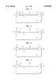
- FIGS. 1 and 2are cross sectional views of a partially fabricated integrated circuit (IC) showing the IC before (FIG. 1) and after (FIG. 2) etching of the sacrificial oxide and are useful in understanding the invention and illustrative of the problem of bird's beak pull back.
- ICintegrated circuit
- FIGS. 3 and 4are cross sectional views of a partially fabricated IC showing the IC before (FIG. 3) and after (FIG. 4) etching of the sacrificial oxide and are useful in understanding the invention and illustrative of the substantial elimination of the problem of bird's beak pull back when the integrated circuit device is processed in accordance with the present invention.
- reference numeral 11denotes a substrate which may, for example, be silicon, epitaxial silicon, or doped silicon.
- Reference numeral 13denotes a field oxide or other isolation oxide which may be formed by a variety of methods known to those skilled in the art, including the popular LOCOS ("local oxidation of silicon") or poly-buffered LOCOS process.
- Reference numeral 17denotes a grown oxide, often termed "a sacrificial oxide".
- the thickness of oxide 17is typically 150 ⁇ 50 ⁇ but may be more or less than this thickness.
- One or more ion implantation stepsare performed by methods also well known to those skilled in the art.
- dopantssuch as arsenic, boron, phosphorus and boron difluoride are employed for ion implantation.
- Some of the implanted dopant speciesare denoted by reference numeral 19.
- Other species implanted to possible greater depthare not shown for reasons of clarity.
- the ion implantation stepmay be performed to form an n-tub or a p-tub, or may be performed to adjust the threshold voltage of the yet-to-be completed devices.
- the surface 21 of the field oxide 13is undesirably altered causing the etch characteristics of the surface region 21 of the field oxide 13 to change such that the etch rate is significantly increased. If etching of the sacrificial oxide layer 17 were to be carried out at this stage, then as shown in FIG. 2, etching can result in significant and undesirable height reduction of the field oxide 13 and may also cause exposure of a portion of the substrate 25 previously protected by the field oxide 13, i.e. bird's beak pull back.
- the deviceprior to etching of the sacrificial oxide layer 17, the device is rapidly thermally annealed.
- This thermal annealingtends to eliminate or retard the effects of the damage incurred to the surface of the field oxide 13 during ion implantation, thereby slowing the etch rate of the surface 21 of the field oxide 13.
- the rapid thermal annealingis preferably achieved by quickly ramping up the temperature of the device, for example, at a rate of from about 25° C./sec. to 150° C./sec. (preferably 45° C./sec. to 55° C./sec.) to a temperature of from about 700° C. to 1100° C. (preferably 800° C. to 1000° C. and most preferably about 900° C.) for about from 5 to 60 seconds (preferably about 30 seconds) in an inert atmosphere, an oxygen atmosphere or preferably in a mixture of an inert atmosphere, such as nitrogen or other non-reactive gas, mixed with from 2% to up to 100% oxygen by volume (preferably comprising a mixture containing 10 vol. % oxygen).
- annealing temperatures above about 1,100° C.may lead to unwanted diffusion of implanted ions, especially if one combined this higher temperature with a long annealing time. Too low a temperature, e.g. below about 700° C. may lead to too long a required annealing time to be practical to achieve the desired results or may be ineffectual.
- oxygen concentrations greater than about 10%tend to cause increased growth of the sacrificial oxide when combined with high annealing temperatures and/or long annealing times.
- the optimum time of annealingwill depend upon the other parameters as well as the thickness of the sacrificial oxide to be removed and the extent and depth of damage of the field oxide during ion implantation.
- the annealing parameters employedshould not result in the growth of a new oxide layer or substantial thickening of the sacrificial oxide 17.
- the sacrificial oxide layer 17is removed, for example, by an HF wet etch process well known to those skilled in the art.
- the bird's beak pull back problem mentioned previouslyis alleviated because the damage done to field oxide 13 during implantation has been reduced or reversed by the annealing step.
- Subsequent processingmay include the formation, for example, of gates in moat 15, definition of source and drain regions, dielectric deposition, window opening, contact metallization, etc. as is well known to those skilled in the art. Greater details of these and other commonly employed integrated circuit processing techniques can be found with reference to VLSI Technology, 2nd Edition, a text edited by S. M. Sze and published by McGraw-Hill, Inc., 1988, which text is incorporated herein by reference.
Landscapes
- Engineering & Computer Science (AREA)
- Physics & Mathematics (AREA)
- Condensed Matter Physics & Semiconductors (AREA)
- General Physics & Mathematics (AREA)
- Manufacturing & Machinery (AREA)
- Computer Hardware Design (AREA)
- Microelectronics & Electronic Packaging (AREA)
- Power Engineering (AREA)
- Local Oxidation Of Silicon (AREA)
Abstract
Description
Claims (18)
Priority Applications (1)
| Application Number | Priority Date | Filing Date | Title |
|---|---|---|---|
| US08/935,362US5950096A (en) | 1997-09-22 | 1997-09-22 | Process for improving device yield in integrated circuit fabrication |
Applications Claiming Priority (1)
| Application Number | Priority Date | Filing Date | Title |
|---|---|---|---|
| US08/935,362US5950096A (en) | 1997-09-22 | 1997-09-22 | Process for improving device yield in integrated circuit fabrication |
Publications (1)
| Publication Number | Publication Date |
|---|---|
| US5950096Atrue US5950096A (en) | 1999-09-07 |
Family
ID=25466989
Family Applications (1)
| Application Number | Title | Priority Date | Filing Date |
|---|---|---|---|
| US08/935,362Expired - LifetimeUS5950096A (en) | 1997-09-22 | 1997-09-22 | Process for improving device yield in integrated circuit fabrication |
Country Status (1)
| Country | Link |
|---|---|
| US (1) | US5950096A (en) |
Cited By (6)
| Publication number | Priority date | Publication date | Assignee | Title |
|---|---|---|---|---|
| KR20010066620A (en)* | 1999-12-31 | 2001-07-11 | 황인길 | Implant damage recovery method by rapid thermal oxidation |
| US20040161902A1 (en)* | 2002-12-31 | 2004-08-19 | Dongbu Electronics Co., Ltd. | Method for fabricating transistor of semiconductor device |
| US6817903B1 (en) | 2000-08-09 | 2004-11-16 | Cypress Semiconductor Corporation | Process for reducing leakage in an integrated circuit with shallow trench isolated active areas |
| US20070087504A1 (en)* | 2005-10-18 | 2007-04-19 | Pham Tuan D | Integration process flow for flash devices with low gap fill aspect ratio |
| US20080242018A1 (en)* | 2007-03-27 | 2008-10-02 | Walsh Shawn T | Method of reducing channeling of ion implants using a sacrificial scattering layer |
| US20080268627A1 (en)* | 2007-04-30 | 2008-10-30 | Hiroaki Niimi | Transistor performance using a two-step damage anneal |
Citations (5)
| Publication number | Priority date | Publication date | Assignee | Title |
|---|---|---|---|---|
| US5376577A (en)* | 1994-06-30 | 1994-12-27 | Micron Semiconductor, Inc. | Method of forming a low resistive current path between a buried contact and a diffusion region |
| US5650350A (en)* | 1995-08-11 | 1997-07-22 | Micron Technology, Inc. | Semiconductor processing method of forming a static random access memory cell and static random access memory cell |
| US5686346A (en)* | 1996-03-26 | 1997-11-11 | Advanced Micro Devices, Inc. | Method for enhancing field oxide thickness at field oxide perimeters |
| US5744391A (en)* | 1997-01-15 | 1998-04-28 | Taiwan Semiconductor Manufacturing Company Ltd. | Method to improve isolation between EEPROM devices via a field oxide anneal |
| US5861334A (en)* | 1995-08-07 | 1999-01-19 | Hyundai Electronics Industries Co., | Method for fabricating semiconductor device having a buried channel |
- 1997
- 1997-09-22USUS08/935,362patent/US5950096A/ennot_activeExpired - Lifetime
Patent Citations (5)
| Publication number | Priority date | Publication date | Assignee | Title |
|---|---|---|---|---|
| US5376577A (en)* | 1994-06-30 | 1994-12-27 | Micron Semiconductor, Inc. | Method of forming a low resistive current path between a buried contact and a diffusion region |
| US5861334A (en)* | 1995-08-07 | 1999-01-19 | Hyundai Electronics Industries Co., | Method for fabricating semiconductor device having a buried channel |
| US5650350A (en)* | 1995-08-11 | 1997-07-22 | Micron Technology, Inc. | Semiconductor processing method of forming a static random access memory cell and static random access memory cell |
| US5686346A (en)* | 1996-03-26 | 1997-11-11 | Advanced Micro Devices, Inc. | Method for enhancing field oxide thickness at field oxide perimeters |
| US5744391A (en)* | 1997-01-15 | 1998-04-28 | Taiwan Semiconductor Manufacturing Company Ltd. | Method to improve isolation between EEPROM devices via a field oxide anneal |
Cited By (12)
| Publication number | Priority date | Publication date | Assignee | Title |
|---|---|---|---|---|
| KR20010066620A (en)* | 1999-12-31 | 2001-07-11 | 황인길 | Implant damage recovery method by rapid thermal oxidation |
| US6817903B1 (en) | 2000-08-09 | 2004-11-16 | Cypress Semiconductor Corporation | Process for reducing leakage in an integrated circuit with shallow trench isolated active areas |
| US20040161902A1 (en)* | 2002-12-31 | 2004-08-19 | Dongbu Electronics Co., Ltd. | Method for fabricating transistor of semiconductor device |
| US20070087504A1 (en)* | 2005-10-18 | 2007-04-19 | Pham Tuan D | Integration process flow for flash devices with low gap fill aspect ratio |
| US7541240B2 (en)* | 2005-10-18 | 2009-06-02 | Sandisk Corporation | Integration process flow for flash devices with low gap fill aspect ratio |
| KR101029696B1 (en) | 2005-10-18 | 2011-04-18 | 쌘디스크 코포레이션 | Integration process flow for flash devices with low gap fill aspect ratio |
| US20080242018A1 (en)* | 2007-03-27 | 2008-10-02 | Walsh Shawn T | Method of reducing channeling of ion implants using a sacrificial scattering layer |
| US7927987B2 (en)* | 2007-03-27 | 2011-04-19 | Texas Instruments Incorporated | Method of reducing channeling of ion implants using a sacrificial scattering layer |
| US20080268627A1 (en)* | 2007-04-30 | 2008-10-30 | Hiroaki Niimi | Transistor performance using a two-step damage anneal |
| US8828855B2 (en)* | 2007-04-30 | 2014-09-09 | Texas Instruments Incorporated | Transistor performance using a two-step damage anneal |
| US9029251B2 (en) | 2007-04-30 | 2015-05-12 | Texas Instruments Incorporated | Transistor performance using a two-step damage anneal |
| US9054056B2 (en) | 2007-04-30 | 2015-06-09 | Texas Instruments Incorporated | Transistor performance using a two-step damage anneal |
Similar Documents
| Publication | Publication Date | Title |
|---|---|---|
| US5846857A (en) | CMOS processing employing removable sidewall spacers for independently optimized N- and P-channel transistor performance | |
| US7402870B2 (en) | Ultra shallow junction formation by epitaxial interface limited diffusion | |
| JP3273636B2 (en) | Integrated circuit and manufacturing method thereof | |
| US4912062A (en) | Method of eliminating bird's beaks when forming field oxide without nitride mask | |
| US6472283B1 (en) | MOS transistor processing utilizing UV-nitride removable spacer and HF etch | |
| US6344396B1 (en) | Removable spacer technology using ion implantation for forming asymmetric MOS transistors | |
| US5344787A (en) | Latid implants for increasing the effective width of transistor elements in a semiconductor device | |
| US6900092B2 (en) | Surface engineering to prevent epi growth on gate poly during selective epi processing | |
| US5895252A (en) | Field oxidation by implanted oxygen (FIMOX) | |
| US6258695B1 (en) | Dislocation suppression by carbon incorporation | |
| US6235560B1 (en) | Silicon-germanium transistor and associated methods | |
| US6429083B1 (en) | Removable spacer technology using ion implantation to augment etch rate differences of spacer materials | |
| EP0053683B1 (en) | Method of making integrated circuit igfet devices | |
| EP0087462A4 (en) | Process for manufacturing an integrated circuit structure. | |
| US5795809A (en) | Semiconductor wafer fabrication process including gettering utilizing a combined oxidation technique | |
| US5950096A (en) | Process for improving device yield in integrated circuit fabrication | |
| US6284672B1 (en) | Method of forming a super-shallow amorphous layer in silicon | |
| US6074933A (en) | Integrated circuit fabrication | |
| US6342423B1 (en) | MOS-type transistor processing utilizing UV-nitride removable spacer and HF etch | |
| US6291311B2 (en) | Semiconductor device and method for producing same | |
| US5612247A (en) | Method for fabricating isolation region for a semiconductor device | |
| JP3328600B2 (en) | Fabrication process for bipolar and BICMOS devices | |
| JPH07273121A (en) | Method for manufacturing semiconductor device | |
| KR101006506B1 (en) | Method of manufacturing semiconductor device | |
| JP2629615B2 (en) | Method for manufacturing semiconductor device |
Legal Events
| Date | Code | Title | Description |
|---|---|---|---|
| AS | Assignment | Owner name:LUCENT TECHNOLOGIES INC., NEW JERSEY Free format text:ASSIGNMENT OF ASSIGNORS INTEREST;ASSIGNORS:HUANG, ROBERT Y.S.;KUEHNE, STEPHEN CARL;LIU, JANE QIAN;AND OTHERS;REEL/FRAME:008729/0758 Effective date:19970917 | |
| STCF | Information on status: patent grant | Free format text:PATENTED CASE | |
| FEPP | Fee payment procedure | Free format text:PAYOR NUMBER ASSIGNED (ORIGINAL EVENT CODE: ASPN); ENTITY STATUS OF PATENT OWNER: LARGE ENTITY | |
| AS | Assignment | Owner name:THE CHASE MANHATTAN BANK, AS COLLATERAL AGENT, TEX Free format text:CONDITIONAL ASSIGNMENT OF AND SECURITY INTEREST IN PATENT RIGHTS;ASSIGNOR:LUCENT TECHNOLOGIES INC. (DE CORPORATION);REEL/FRAME:011722/0048 Effective date:20010222 | |
| FPAY | Fee payment | Year of fee payment:4 | |
| AS | Assignment | Owner name:LUCENT TECHNOLOGIES INC., NEW JERSEY Free format text:TERMINATION AND RELEASE OF SECURITY INTEREST IN PATENT RIGHTS;ASSIGNOR:JPMORGAN CHASE BANK, N.A. (FORMERLY KNOWN AS THE CHASE MANHATTAN BANK), AS ADMINISTRATIVE AGENT;REEL/FRAME:018590/0047 Effective date:20061130 | |
| FPAY | Fee payment | Year of fee payment:8 | |
| FPAY | Fee payment | Year of fee payment:12 | |
| AS | Assignment | Owner name:OMEGA CREDIT OPPORTUNITIES MASTER FUND, LP, NEW YORK Free format text:SECURITY INTEREST;ASSIGNOR:WSOU INVESTMENTS, LLC;REEL/FRAME:043966/0574 Effective date:20170822 Owner name:OMEGA CREDIT OPPORTUNITIES MASTER FUND, LP, NEW YO Free format text:SECURITY INTEREST;ASSIGNOR:WSOU INVESTMENTS, LLC;REEL/FRAME:043966/0574 Effective date:20170822 | |
| AS | Assignment | Owner name:WSOU INVESTMENTS, LLC, CALIFORNIA Free format text:ASSIGNMENT OF ASSIGNORS INTEREST;ASSIGNOR:ALCATEL LUCENT;REEL/FRAME:044000/0053 Effective date:20170722 | |
| AS | Assignment | Owner name:WSOU INVESTMENTS, LLC, CALIFORNIA Free format text:RELEASE BY SECURED PARTY;ASSIGNOR:OCO OPPORTUNITIES MASTER FUND, L.P. (F/K/A OMEGA CREDIT OPPORTUNITIES MASTER FUND LP;REEL/FRAME:049246/0405 Effective date:20190516 | |
| AS | Assignment | Owner name:OT WSOU TERRIER HOLDINGS, LLC, CALIFORNIA Free format text:SECURITY INTEREST;ASSIGNOR:WSOU INVESTMENTS, LLC;REEL/FRAME:056990/0081 Effective date:20210528 |