US5949362A - Digital-to-analog converter including current cell matrix with enhanced linearity and associated methods - Google Patents
Digital-to-analog converter including current cell matrix with enhanced linearity and associated methodsDownload PDFInfo
- Publication number
- US5949362A US5949362AUS08/916,569US91656997AUS5949362AUS 5949362 AUS5949362 AUS 5949362AUS 91656997 AUS91656997 AUS 91656997AUS 5949362 AUS5949362 AUS 5949362A
- Authority
- US
- United States
- Prior art keywords
- current source
- array
- source cells
- operating
- dac
- Prior art date
- Legal status (The legal status is an assumption and is not a legal conclusion. Google has not performed a legal analysis and makes no representation as to the accuracy of the status listed.)
- Expired - Lifetime
Links
Images


Classifications
- H—ELECTRICITY
- H03—ELECTRONIC CIRCUITRY
- H03M—CODING; DECODING; CODE CONVERSION IN GENERAL
- H03M1/00—Analogue/digital conversion; Digital/analogue conversion
- H03M1/66—Digital/analogue converters
- H—ELECTRICITY
- H03—ELECTRONIC CIRCUITRY
- H03M—CODING; DECODING; CODE CONVERSION IN GENERAL
- H03M1/00—Analogue/digital conversion; Digital/analogue conversion
- H03M1/06—Continuously compensating for, or preventing, undesired influence of physical parameters
- H03M1/0617—Continuously compensating for, or preventing, undesired influence of physical parameters characterised by the use of methods or means not specific to a particular type of detrimental influence
- H03M1/0634—Continuously compensating for, or preventing, undesired influence of physical parameters characterised by the use of methods or means not specific to a particular type of detrimental influence by averaging out the errors, e.g. using sliding scale
- H03M1/0643—Continuously compensating for, or preventing, undesired influence of physical parameters characterised by the use of methods or means not specific to a particular type of detrimental influence by averaging out the errors, e.g. using sliding scale in the spatial domain
- H03M1/0651—Continuously compensating for, or preventing, undesired influence of physical parameters characterised by the use of methods or means not specific to a particular type of detrimental influence by averaging out the errors, e.g. using sliding scale in the spatial domain by selecting the quantisation value generators in a non-sequential order, e.g. symmetrical
- H—ELECTRICITY
- H03—ELECTRONIC CIRCUITRY
- H03M—CODING; DECODING; CODE CONVERSION IN GENERAL
- H03M1/00—Analogue/digital conversion; Digital/analogue conversion
- H03M1/66—Digital/analogue converters
- H03M1/68—Digital/analogue converters with conversions of different sensitivity, i.e. one conversion relating to the more significant digital bits and another conversion to the less significant bits
- H03M1/682—Digital/analogue converters with conversions of different sensitivity, i.e. one conversion relating to the more significant digital bits and another conversion to the less significant bits both converters being of the unary decoded type
- H03M1/685—Digital/analogue converters with conversions of different sensitivity, i.e. one conversion relating to the more significant digital bits and another conversion to the less significant bits both converters being of the unary decoded type the quantisation value generators of both converters being arranged in a common two-dimensional array
- H—ELECTRICITY
- H03—ELECTRONIC CIRCUITRY
- H03M—CODING; DECODING; CODE CONVERSION IN GENERAL
- H03M1/00—Analogue/digital conversion; Digital/analogue conversion
- H03M1/66—Digital/analogue converters
- H03M1/74—Simultaneous conversion
- H03M1/742—Simultaneous conversion using current sources as quantisation value generators
- H03M1/747—Simultaneous conversion using current sources as quantisation value generators with equal currents which are switched by unary decoded digital signals
Definitions
- the present applicationrelates to the field of electronic circuits, and, more particularly, to a digital-to-analog converter (DAC) and related methods.
- DACdigital-to-analog converter
- Digital-to-analog convertersare widely used for converting digital signals to corresponding analog signals for many electronic circuits.
- a high resolution, high speed digital-to-analog convertermay find applications in cellular base stations, wireless communications, direct digital frequency synthesis, signal reconstruction, test equipment, high resolution imaging systems and arbitrary waveform generators, for example.
- the DACincludes binarily scaled constant current sources with associated switch cells employing bipolar transistors to direct the bit currents either to a current summing bus or to ground.
- Each of the switch cellsincludes a first differential transistor pair driving a second differential pair of current switching transistors.
- a DAC for video applicationsis disclosed in an article entitled "A Low Glitch 10-bit 75-MHZ CMOS Video D/A Converter" by Wu et al. in the IEEE Journal of Solid-State Circuits, Vol. 30, No. 1, January 1995.
- the DACincludes a segmented antisymmetric switching sequence and an asymmetrical switching buffer.
- the DACincludes a large number of non-weighted current sources for the seven most significant bits, and weighted current sources for the three least significant bits.
- the current sourcesmay be non-uniform for various reasons, such as layout mismatch, thermal distribution, and process deviation.
- a segmented antisymmetric switching sequenceis disclosed to suppress the superposition of graded error, symmetrical error, and especially random error.
- the asymmetrical switch controlavoids simultaneously turning off the differential switching transistors completely, but allow simultaneous turn-on for a short period of time.
- mismatchis the process that causes time-independent random variations in physical quantities of identical designed devices, and is a limiting factor in DACs, for example.
- Many known processes which cause mismatchinginclude distribution of ion-implanted, diffused, or substrate ions; local mobility fluctuations; oxide granularity; oxide charges; etc.
- edge roughnessseems not to be a major mismatch factor, leaving mobility and gate oxides as possible mismatch causes.
- a DACwhich in one embodiment comprises a first array of current source cells extending in first and second transverse directions, and two-dimensional symmetrical control means for operating predetermined current source cells based upon a portion of digital input words and in a symmetrical sequence in both the first and second directions with respect to a medial position of the first array.
- the medial positionpreferably defines a centroid for the first array. Accordingly, the DAC is less susceptible to variations in threshold voltage and current factor as may otherwise be caused by process gradients, for example.
- the first arraymay also include first and second rows of current source cells.
- the two-dimensional symmetrical control meansmay comprise a decoder for generating the control signals, and means for operating the first row with even control signals and for operating the second row with odd control signals.
- the current source cellsmay have substantially equal output currents.
- the two-dimensional symmetrical control meansmay preferably include a decoder for generating a plurality of control signals based upon predetermined most significant bits (MSBs) of digital input words.
- the decoderis preferably a thermometer decoder.
- the first arrayfurther comprises a plurality of second current source cells
- the two-dimensional symmetrical control meansfurther comprises LSB cell control means for operating the plurality of second current source cells based upon predetermined LSBs of digital input words.
- at least some of the second plurality of current source cellsare positioned in a medial portion of the first array.
- each of the second plurality of current source cellspreferably comprises a plurality of current source devices which, in turn, may have substantially same output currents.
- the LSB cell control meansoperates predetermined ones of the current source devices for binarily weighting the cell outputs.
- the second plurality of current source cellscomprises weighted output current source cells for the LSBs.
- the DACmay include a substantially identical second array adjacent the first array.
- the two-dimensional symmetrical control meansmay include geometrical averaging means for operating the current source cells in the first and second arrays in pairs and in a substantially true mirror image sequence.
- the geometrical averaging meansmay alternately operate the current source cells in the first and second arrays in pairs and in a substantially inverted mirror image sequence.
- the DACmay also include output means connected to the array for producing analog output signals based upon digital input words.
- Each of the current source cellsmay comprise a plurality of current source devices positioned in side-by-side or in-line relation. Alternately, each of the current source cells may include a plurality of current source devices positioned in a generally rectangular pattern of rows and columns. Each of the current source devices of a cell may comprise at least one CMOS transistor. In addition, dummy cells may be provided adjacent the array to thereby reduce undesirable edge effects.
- Another embodiment of DACcomprises a first array of current source cells extending in first and second transverse directions, with each current cell comprising a plurality of current source devices arranged in a line.
- This embodimentfurther includes two-dimensional symmetrical control means for operating predetermined current source cells of the first array based upon most significant bits (MSBs) of digital input words and in a symmetrical sequence in both the first and second directions with respect to a medial position of the first array.
- MSBsmost significant bits
- additional current source devicesare positioned in-line with the current source devices of the array to define a V-shaped diagonal pattern through the array.
- this embodimentpreferably further includes LSB control means for operating the additional current source devices based upon the LSBs of digital input words.
- a DACcomprises an array of current source devices, and matrix switch control means for operating predetermined current source devices in a sequential matrix pattern.
- the matrix patternis preferably defined by a plurality of generally rectangular submatrix patterns, with each submatrix pattern, in turn, being a substantially mirror image of adjacent submatrices.
- a method aspect of the inventionis for operating a DAC comprises a first array of current source cells extending in first and second transverse directions.
- the methodpreferably comprises the step of operating predetermined current source cells of the first array based upon at least a portion of digital input words and in a symmetrical sequence in both the first and second directions with respect to a medial position of the first array.
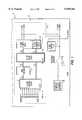
- FIG. 1is a schematic block diagram of a DAC in accordance with the present invention.
- FIG. 2is a schematic diagram of a first current source cell matrix embodiment as used in the DAC of FIG. 1 and with one current source cell shown in an enlarged portion.
- FIG. 3is a schematic diagram of a second current source cell matrix embodiment as also used in the DAC of FIG. 1.
- FIG. 4is a schematic diagram of a third current source cell matrix embodiment as also used in the DAC of FIG. 1.
- FIG. 5is a schematic diagram of a fourth current source cell matrix embodiment as also used in the DAC of FIG. 1.
- FIG. 6is a schematic diagram of a fifth current source cell matrix embodiment as also used in the DAC of FIG. 1.
- the DAC 11uses a segmented architecture to reduce both differential non-linearity (DNL) and glitch energy.
- Input data wordsfirst pass through the illustrated 10-bit master latch 15 which is transparent when the clock signal is low.
- the five most significant bits (MSBs)then pass through a 5-to-31 thermometer decoder 17 in which an increasing number of output signals go high as the input code is increased as would be readily understood by those skilled in the art.
- These 31 control signalsthen pass through the illustrated 36-bit slave D-latch 21 which is transparent when the clock signal is high.
- the master-slave arrangementsynchronizes the data to reduce glitch energy as would also be readily understood by those skilled in the art.
- the 36 outputs from the slave D-latch 21control the current steering switches in the current source array 25.
- the 31 MSB current cells(segments) each have a value of 1/32 of the full-scale current output current.
- the 5 LSB current cellsare binary weighted fractions of the segment current, that is, 1/2, 1/4, 1/8, 1/16 and 1/32 for bits D4 to D0, respectively.
- eight additional reference current cells 27are connected in a feedback configuration with the reference amplifier 30 to establish a desired full-scale output current for a plurality of DACs as may typically be included on a chip, and as would be readily understood by those skilled in the art.
- the two COMP terminalsconnect to external decoupling capacitors, not shown, which absorb switching transients on these bias lines for improved dynamic performance.
- a bandgap voltage reference 28provides a precision voltage to the reference amplifier 30 for use in establishing the full scale current as will be readily appreciated by those skilled in the art.
- 10-bit DACsare described wherein the input words are separated into 5 MSBs and 5 LSBs.
- Those of skill in the artwill appreciate that larger or smaller DACs are contemplated by the invention and that the division of MSBs and LSBs may also determined as desired for a particular DAC.
- This embodimentcomprises a first array 31 of current source cells 32 positioned to the right of the dashed line 33.
- the cells of the first array 31extend in first and second transverse directions.
- two-dimensional symmetrical control means 35as schematically illustrated is provided for operating predetermined current source cell of the first array 31 based upon at least a portion of digital input words and in a symmetrical sequence in both the first and second directions with respect to a medial position of the first array.
- the medial positionpreferably defines a centroid for the first array as shown by the illustrated imaginary point labeled 39.
- the two-dimensional symmetrical controller 35may be provided by the decoder 17 and its associated circuitry which control the individual current source cells 32 as would be readily understood by those skilled in the art. As an increasing number of current sources are switched, the current sources labeled 1-31 are sequentially operated. Accordingly, the DAC 25 is less susceptible to variations in threshold voltage and current factor as may otherwise be caused by process gradients, for example.
- the first array 31may also include first and second rows 34, 36 of current source cells 32.
- the two-dimensional symmetrical control means 35generates a plurality of control signals which are coupled to the array so that the first row is operated with even control signals and the second row is operated with odd control signals.
- the even signalsincrease from left to right in the first array 31, while the odd signals decrease from left to right to thereby provide the symmetrical switching.
- the signalsalso symmetrically switch between the first and second rows to provide the two-dimensional symmetry and its associated improvement in reducing non-linearities caused by process gradients.
- the current source cells 32 labeled 1-31are for the MSBs and therefore have substantially equal output currents.
- Dummy cells 37are positioned at the right of the first array 31 to thereby reduce undesirable effects as would otherwise be caused at the active edge cells as would be readily appreciated by those skilled in the art.
- a current source cell 32includes a 4 ⁇ 4 arrangement of current source devices, such as CMOS transistors for example.
- CMOS transistorsfor example.
- Other arrangementsare also contemplated by the invention and an in-line arrangement is described in further embodiments, for example.
- the first array 31further comprises a plurality of second current source cells or LSB cells 32a labeled as D0 through D4 in the figure.
- the two-dimensional symmetrical control means 35further comprises LSB cell control means for operating the plurality of LSB current source cells 32a based upon predetermined LSBs of digital input words.
- LSB current source cellsD1-D4 are positioned in a medial portion of the first array to also reduce the effects of process gradients.
- the LSB cells 32amay have binarily weighted output currents as would also be readily understood by those skilled in the art.
- the DAC 25may include a substantially identical second array 38 adjacent the first array 31.
- the two-dimensional symmetrical control means 35may include geometrical averaging means for operating the current source cells 32 in the first and second arrays in pairs and in a substantially true mirror image sequence as shown in the illustrated embodiment of FIG. 2. For example, both cells of a pair may be connected to the same respective control signal and the output of each cell is half the desired combined output current.
- the geometrical averaging meansmay alternately operate the current source cells 32 in the first and second arrays in pairs and in a substantially inverted mirror image sequence as will be seen in later embodiments.
- the LSB current source cells 32aare also substantially mirrored between the two arrays 31, 38.
- the LSB D0is generally the smallest current that can be produced, has the least effect on accuracy, and is not duplicated in the second array 38 as will be appreciated by those skilled in the art.
- FIG. 3a second embodiment of a current source cell matrix 45 is now described.
- the two-dimensional symmetrical control meansis not shown in this embodiment for greater clarity; rather, the numbers indicate the switching sequence for the MSB cells and the LSB cells.
- the current cells 46are defined by a plurality of current source devices 47, sixteen in the illustrated embodiment, connected in an in-line configuration.
- a different variation of mirror symmetryis also shown between the left hand array 58 and the right hand array 51.
- an inverted mirror image symmetryis provided about dashed line 48, as contrasted to the true mirror symmetry of the embodiment shown in FIG. 2.
- the illustrated matrix embodiment 45enjoys the same benefits and advantages from both symmetrical switching and also geometrical averaging as discussed extensively above.
- the matrix 45also has a slightly different treatment for the LSB cells.
- the LSB cellsare formed by selectively connecting predetermined and generally spaced apart ones of the current source devices 47a in the medial row between the upper and lower banks of MSB current source devices.
- the D4 LSB cellis shown by the line 48 connecting the current source devices labeled 4 in the medial row.
- the other LSBsare configured similarly, with the number of connected current source devices based upon the desired scaled output current. Dummy current source devices, not shown, also desirably fill in the spaces between the banks and surround the overall active portion of the matrix 45.
- a third matrix embodiment 65is understood with reference to FIG. 4.
- This embodimentincludes an overall array of current source devices 67 similar to the embodiment shown in FIG. 3. However, in the matrix 65 of FIG. 4, the first and second arrays are in upper and lower positions relative to the dashed line 68. In addition, each cell 46 for the MSBs extends laterally.
- the LSB current source devices 67aare arranged between the upper and lower arrays and are connected as described above with reference to FIG. 3.
- This matrix embodiment 65also has inverted mirror symmetry like the matrix embodiment 45 shown in FIG. 3. Dummy cells, not shown, are also desirably included in the matrix 65 as would be readily understood by those skilled in the art.
- a fourth embodiment of a current cell/device matrix 85is understood with reference to FIG. 5.
- the arraysare above and below the dashed line 98 and the LSB current source devices 87a are connected from rows of current source devices 87 defining the MSB current cells.
- the arrangement of LSB current source devicesis such as to define a V-shaped pattern in the upper array, and to define an X-shape in the overall matrix 85.
- the positioning of the LSB current source devices 87aprovides for a further enhancement of linearity even in the presence of process gradients as will be readily understood by those skilled in the art. Those of skill in the art will readily appreciate other configurations of positioning of the LSB current source devices within an overall arrangement of current source devices.
- a DAC current source matrix 105includes an array of current source devices 107 for the MSBs and with interspersed devices 107b as indicated for the LSBs.
- the matrix 105has a matrix pattern defined by a plurality of generally rectangular submatrix patterns, each defined between the illustrated horizontal grid lines 110 and the vertical grid lines 111. Each submatrix pattern, in turn, is a substantially mirror image of adjacent submatrices as illustrated.
- the LSB current source devices 107aare positioned at the submatrix corners and are assigned to provide geometrical spacing and the proper combined scaled output current. This embodiment also enjoys the benefits of symmetrical switching, as well as geometrical averaging.
- a method aspect of operating the DAC including the current source cell matrix 25includes operating predetermined current source cells of the first array 31 based upon at least a portion of digital input words and in a symmetrical sequence in both the first and second directions with respect to a medial position 39 of the first array.
- the methodmay also include generating a plurality of control signals, and operating the first row with even control signals and operating the second row with odd control signals.
- the first arraymay further comprise a plurality of second current source cells for the LSBs, and the method may further comprise the step of operating the plurality of second current source cells based upon LSBs of digital input words.
- the matrix 25may also include a second array 38 adjacent the first array and being substantially identical thereto. Accordingly, the method may further include the step of operating the current source cells in the first and second arrays in pairs and in a substantially true mirror image sequence or in an inverted mirror image sequence.
Landscapes
- Engineering & Computer Science (AREA)
- Theoretical Computer Science (AREA)
- Analogue/Digital Conversion (AREA)
Abstract
Description
Claims (51)
Priority Applications (5)
| Application Number | Priority Date | Filing Date | Title |
|---|---|---|---|
| US08/916,569US5949362A (en) | 1997-08-22 | 1997-08-22 | Digital-to-analog converter including current cell matrix with enhanced linearity and associated methods |
| EP98402079AEP0898374B1 (en) | 1997-08-22 | 1998-08-19 | Digital-to-analog converter including current cell matrix with enhanced linearity and associated methods |
| DE69836782TDE69836782T2 (en) | 1997-08-22 | 1998-08-19 | Digital-to-analogue converter with a stream source matrix with improved linearity and associated methods |
| KR1019980034127AKR100530890B1 (en) | 1997-08-22 | 1998-08-22 | Digital-to-analog converters and related methods, including current cell matrices with improved linearity. |
| JP10236765AJPH11163728A (en) | 1997-08-22 | 1998-08-24 | D/a converter having current cell matrix to improve linearity and its control method |
Applications Claiming Priority (1)
| Application Number | Priority Date | Filing Date | Title |
|---|---|---|---|
| US08/916,569US5949362A (en) | 1997-08-22 | 1997-08-22 | Digital-to-analog converter including current cell matrix with enhanced linearity and associated methods |
Publications (1)
| Publication Number | Publication Date |
|---|---|
| US5949362Atrue US5949362A (en) | 1999-09-07 |
Family
ID=25437486
Family Applications (1)
| Application Number | Title | Priority Date | Filing Date |
|---|---|---|---|
| US08/916,569Expired - LifetimeUS5949362A (en) | 1997-08-22 | 1997-08-22 | Digital-to-analog converter including current cell matrix with enhanced linearity and associated methods |
Country Status (5)
| Country | Link |
|---|---|
| US (1) | US5949362A (en) |
| EP (1) | EP0898374B1 (en) |
| JP (1) | JPH11163728A (en) |
| KR (1) | KR100530890B1 (en) |
| DE (1) | DE69836782T2 (en) |
Cited By (43)
| Publication number | Priority date | Publication date | Assignee | Title |
|---|---|---|---|---|
| US6081217A (en)* | 1998-07-13 | 2000-06-27 | Tenx Technology, Inc. | Decoder for 2-dimensional input devices |
| US6118398A (en)* | 1998-09-08 | 2000-09-12 | Intersil Corporation | Digital-to-analog converter including current sources operable in a predetermined sequence and associated methods |
| US6281824B1 (en)* | 1997-03-28 | 2001-08-28 | Sony Corporation | Digital to analog converter using constant current sources |
| US6337644B1 (en)* | 1998-06-25 | 2002-01-08 | Seiko Epson Corporation | Constant-current generation circuit, digital/analog conversion circuit, and image processor |
| US6339391B1 (en)* | 1999-12-13 | 2002-01-15 | Lsi Logic Corporation | Method and apparatus for optimizing crossover voltage for differential pair switches in a current-steering digital-to-analog converter or the like |
| US6346901B1 (en)* | 1998-12-24 | 2002-02-12 | Motorola, Inc. | Digital-to-analog conversion circuit |
| US6433721B2 (en) | 2000-06-23 | 2002-08-13 | Matsushita Electric Industrial Co., Ltd. | Current source cell arrangement, method of selecting current source cell and current addition type digital-to-analog converter |
| US6452527B2 (en)* | 2000-06-28 | 2002-09-17 | Matsushita Electric Industrial Co., Ltd. | Current adding type D/A converter |
| US6496131B2 (en) | 2000-09-26 | 2002-12-17 | Nec Corporation | Capacitor-array D/A converter including a thermometer decoder and a capacitor array |
| US6501402B2 (en) | 2001-05-09 | 2002-12-31 | Broadcom Corporation | Digital-to-analogue converter using an array of current sources |
| US6507304B1 (en)* | 2002-05-02 | 2003-01-14 | National Semiconductor Corporation | Current steering segmented DAC system |
| US20030169194A1 (en)* | 2002-03-05 | 2003-09-11 | Masami Aiura | Method of selecting cells for input code in a digital-to-analog converter |
| US6720898B1 (en)* | 2003-04-10 | 2004-04-13 | Maxim Integrated Products, Inc. | Current source array for high speed, high resolution current steering DACs |
| US6734815B1 (en)* | 2003-03-25 | 2004-05-11 | T-Ram, Inc. | Geometric D/A converter for a delay-locked loop |
| US20040125005A1 (en)* | 2002-12-25 | 2004-07-01 | Denson Corporation | Digital to analogue converter and analogue to digital converter using the same |
| US20040125004A1 (en)* | 2002-12-25 | 2004-07-01 | Renesas Technology Corporation | D/A converter for converting plurality of digital signals simultaneously |
| KR100456830B1 (en)* | 2002-10-22 | 2004-11-10 | 삼성전자주식회사 | Transistor array and layout method of this array |
| US20050052297A1 (en)* | 2002-05-27 | 2005-03-10 | Nokia Corporation | Method for calibrating a digital-to-analog converter and a digital-to-analog converter |
| US20050093729A1 (en)* | 2003-11-03 | 2005-05-05 | Heng-Chih Lin | Guaranteed monotonic digital to analog converter |
| US6975260B1 (en) | 2003-03-25 | 2005-12-13 | T-Ram, Inc. | Geometric D/A converter for a delay-locked loop |
| US7095348B1 (en) | 2000-05-23 | 2006-08-22 | Marvell International Ltd. | Communication driver |
| US7113121B1 (en) | 2000-05-23 | 2006-09-26 | Marvell International Ltd. | Communication driver |
| DE102005017305A1 (en)* | 2005-04-14 | 2006-10-19 | Infineon Technologies Ag | Thirteen-bit-digital to analog converter, has segments of partitioned cell arrangement with converter cells and redundant converter cells and self calibration unit with individual reference cell to calibrate converter cells |
| US7194037B1 (en) | 2000-05-23 | 2007-03-20 | Marvell International Ltd. | Active replica transformer hybrid |
| CN1320764C (en)* | 2000-10-26 | 2007-06-06 | 富士通株式会社 | segment circuit |
| US7312662B1 (en) | 2005-08-09 | 2007-12-25 | Marvell International Ltd. | Cascode gain boosting system and method for a transmitter |
| US7312739B1 (en) | 2000-05-23 | 2007-12-25 | Marvell International Ltd. | Communication driver |
| US7327995B1 (en) | 2000-07-31 | 2008-02-05 | Marvell International Ltd. | Active resistance summer for a transformer hybrid |
| US20080036635A1 (en)* | 2006-08-11 | 2008-02-14 | Realtek Semiconductor Corp. | Digital-to-analog converter and method thereof |
| US7433665B1 (en) | 2000-07-31 | 2008-10-07 | Marvell International Ltd. | Apparatus and method for converting single-ended signals to a differential signal, and transceiver employing same |
| US20090073012A1 (en)* | 2007-09-14 | 2009-03-19 | Realtek Semiconductor Corp. | Self-calibrating digital-to-analog converter and method thereof |
| US7577892B1 (en) | 2005-08-25 | 2009-08-18 | Marvell International Ltd | High speed iterative decoder |
| US7606547B1 (en) | 2000-07-31 | 2009-10-20 | Marvell International Ltd. | Active resistance summer for a transformer hybrid |
| USRE40971E1 (en) | 2000-12-18 | 2009-11-17 | Marvell International Ltd. | Direct drive programmable high speed power digital-to-analog converter |
| US7675450B1 (en)* | 2007-06-13 | 2010-03-09 | Aquantia Corporation | Digital-to-analog converter (DAC) for high frequency and high resolution environments |
| US20100164766A1 (en)* | 2008-12-31 | 2010-07-01 | Fang-Shi Jordan Lai | DAC Variation-Tracking Calibration |
| USRE41831E1 (en) | 2000-05-23 | 2010-10-19 | Marvell International Ltd. | Class B driver |
| CN1909377B (en)* | 2000-10-26 | 2011-10-05 | 富士通半导体股份有限公司 | segment circuit |
| US8232903B2 (en) | 2010-04-30 | 2012-07-31 | Taiwan Semiconductor Manufacturing Co., Ltd. | Finger-split and finger-shifted technique for high-precision current mirror |
| US20140304575A1 (en)* | 2011-12-06 | 2014-10-09 | Samsung Electronics Co., Ltd. | Digital-analog conversion apparatus and method |
| US9583631B1 (en) | 2015-12-04 | 2017-02-28 | Via Alliance Semiconductor Co., Ltd. | Transistors with uniform density of poly silicon |
| TWI577138B (en)* | 2015-12-04 | 2017-04-01 | 上海兆芯集成電路有限公司 | Current source devices |
| CN113810050A (en)* | 2021-11-19 | 2021-12-17 | 深圳百瑞互联技术有限公司 | DAC with concentric parallelogram wiring and output impedance compensation |
Families Citing this family (13)
| Publication number | Priority date | Publication date | Assignee | Title |
|---|---|---|---|---|
| GB2333190B (en)* | 1998-01-08 | 2002-03-27 | Fujitsu Ltd | Cell array circuitry |
| KR100790025B1 (en)* | 2000-04-04 | 2007-12-31 | 엔엑스피 비 브이 | Digital to Analog Converter |
| EP1202459B1 (en)* | 2000-10-26 | 2006-05-10 | Fujitsu Limited | Segmented circuitry |
| JP4674998B2 (en)* | 2001-06-13 | 2011-04-20 | ルネサスエレクトロニクス株式会社 | Folding A / D converter |
| KR100727885B1 (en)* | 2003-05-20 | 2007-06-14 | 학교법인 인하학원 | 10-Bit Digital-to-Analog Converter Using New Glitch Energy Suppression Circuit and New Two-Dimensional Current Cell Switching Sequence |
| CN1813408A (en)* | 2003-06-27 | 2006-08-02 | 皇家飞利浦电子股份有限公司 | A current steering d/a converter with reduced dynamic non-linearities |
| US7199741B2 (en) | 2003-10-24 | 2007-04-03 | Infineon Technologies Ag | Method for digital/analog conversion and corresponding digital/analog converter device |
| DE102004005138B9 (en)* | 2003-10-24 | 2010-11-25 | Infineon Technologies Ag | Method for digital / analog conversion and corresponding digital / analog converter device |
| US6911930B1 (en)* | 2003-12-15 | 2005-06-28 | Infineon Technologies Ag | Cell array with mismatch reduction |
| CN101924561B (en)* | 2010-07-02 | 2013-06-19 | 清华大学 | Current source conduction array used in current-mode digital to analog converter and configuration method thereof |
| KR101226899B1 (en) | 2010-08-17 | 2013-01-28 | 서강대학교산학협력단 | Digital-to-Analog Converter using 2D INL bounded switching scheme |
| JP2018107771A (en)* | 2016-12-28 | 2018-07-05 | 株式会社デンソー | Differential output type d/a converter and a/d converter |
| WO2021171880A1 (en)* | 2020-02-26 | 2021-09-02 | 株式会社テックイデア | Product-sum calculator |
Citations (9)
| Publication number | Priority date | Publication date | Assignee | Title |
|---|---|---|---|---|
| US3995304A (en)* | 1972-01-10 | 1976-11-30 | Teledyne, Inc. | D/A bit switch |
| US4695826A (en)* | 1985-04-17 | 1987-09-22 | Mitsubishi Denki Kabushiki Kaisha | High accuracy digital-to-analog converter having symmetrical current source switching |
| US4812818A (en)* | 1987-02-24 | 1989-03-14 | Brooktree Corporation | Digital-to-analog converter |
| US4859930A (en)* | 1988-02-16 | 1989-08-22 | Schouwenaars Hendrikus J | Current source arrangement |
| US4864215A (en)* | 1988-02-16 | 1989-09-05 | U.S. Philips Corp. | Current source arrangement |
| US5056838A (en)* | 1990-10-24 | 1991-10-15 | General Motors Corporation | Soft touch door handle |
| JPH04162830A (en)* | 1990-10-26 | 1992-06-08 | Nec Corp | D/a converter |
| US5568145A (en)* | 1994-10-19 | 1996-10-22 | Analog Devices, Inc. | MOS current source layout technique to minimize deviation |
| JPH08330966A (en)* | 1995-03-29 | 1996-12-13 | Kawasaki Steel Corp | Current cell type DA converter |
- 1997
- 1997-08-22USUS08/916,569patent/US5949362A/ennot_activeExpired - Lifetime
- 1998
- 1998-08-19DEDE69836782Tpatent/DE69836782T2/ennot_activeExpired - Lifetime
- 1998-08-19EPEP98402079Apatent/EP0898374B1/ennot_activeExpired - Lifetime
- 1998-08-22KRKR1019980034127Apatent/KR100530890B1/ennot_activeExpired - Fee Related
- 1998-08-24JPJP10236765Apatent/JPH11163728A/enactivePending
Patent Citations (9)
| Publication number | Priority date | Publication date | Assignee | Title |
|---|---|---|---|---|
| US3995304A (en)* | 1972-01-10 | 1976-11-30 | Teledyne, Inc. | D/A bit switch |
| US4695826A (en)* | 1985-04-17 | 1987-09-22 | Mitsubishi Denki Kabushiki Kaisha | High accuracy digital-to-analog converter having symmetrical current source switching |
| US4812818A (en)* | 1987-02-24 | 1989-03-14 | Brooktree Corporation | Digital-to-analog converter |
| US4859930A (en)* | 1988-02-16 | 1989-08-22 | Schouwenaars Hendrikus J | Current source arrangement |
| US4864215A (en)* | 1988-02-16 | 1989-09-05 | U.S. Philips Corp. | Current source arrangement |
| US5056838A (en)* | 1990-10-24 | 1991-10-15 | General Motors Corporation | Soft touch door handle |
| JPH04162830A (en)* | 1990-10-26 | 1992-06-08 | Nec Corp | D/a converter |
| US5568145A (en)* | 1994-10-19 | 1996-10-22 | Analog Devices, Inc. | MOS current source layout technique to minimize deviation |
| JPH08330966A (en)* | 1995-03-29 | 1996-12-13 | Kawasaki Steel Corp | Current cell type DA converter |
Non-Patent Citations (12)
| Title |
|---|
| Cornelius A.A. Bastiaansen, et al., "A 10-b 40-MHz 0.8-μm CMOS Current-Output D/A Converter," IEEE Journal of Solid-State Circuits, vol. 26, No. 7, Jul. 1991, pp. 917-921. |
| Cornelius A.A. Bastiaansen, et al., A 10 b 40 MHz 0.8 m CMOS Current Output D/A Converter, IEEE Journal of Solid State Circuits, vol. 26, No. 7, Jul. 1991, pp. 917 921.* |
| Douglas Mercer, "A 16-b D/A Converter with Increased Spurious Free Dynamic Range," IEEE Journal of Solid-State Circuits, vol. 29, No. 10, Oct. 1994, pp. 1180-1185. |
| Douglas Mercer, A 16 b D/A Converter with Increased Spurious Free Dynamic Range, IEEE Journal of Solid State Circuits, vol. 29, No. 10, Oct. 1994, pp. 1180 1185.* |
| Douglas Mercer, et al., "12-b 125 MSPS CMOS D/A Designed For Spectral Performance," ISLPED, Aug. 1996, pp. 243-246. |
| Douglas Mercer, et al., 12 b 125 MSPS CMOS D/A Designed For Spectral Performance, ISLPED, Aug. 1996, pp. 243 246.* |
| Marcel J.M. Pelgrom, et al., "Matching Properties of MOS Transistors," IEEE Journal of Solid-State Circuits, vol. 24, No. 5, Oct. 1989, pp. 1433-1439. |
| Marcel J.M. Pelgrom, et al., Matching Properties of MOS Transistors, IEEE Journal of Solid State Circuits, vol. 24, No. 5, Oct. 1989, pp. 1433 1439.* |
| Takahiro Miki, et al., "An 80-MHz 8-bit CMOS D/A Converter," IEEE Journal of Solid-State Circuits, vol. SC-21, No. 6, Dec. 1986, pp. 983-988. |
| Takahiro Miki, et al., An 80 MHz 8 bit CMOS D/A Converter, IEEE Journal of Solid State Circuits, vol. SC 21, No. 6, Dec. 1986, pp. 983 988.* |
| Tien Yu Wu, et al., A Low Glitch 10 bit MHz CMOS Video D/A Converter, IEEE Journal of Solid State Circuits, vol. 30, No. 1, Jan. 1995, pp. 68 72.* |
| Tien-Yu Wu, et al., "A Low Glitch 10-bit MHz CMOS Video D/A Converter," IEEE Journal of Solid-State Circuits, vol. 30, No. 1, Jan. 1995, pp. 68-72. |
Cited By (76)
| Publication number | Priority date | Publication date | Assignee | Title |
|---|---|---|---|---|
| US6281824B1 (en)* | 1997-03-28 | 2001-08-28 | Sony Corporation | Digital to analog converter using constant current sources |
| US6388598B2 (en)* | 1997-03-28 | 2002-05-14 | Sony Corporation | D/A converter |
| US6337644B1 (en)* | 1998-06-25 | 2002-01-08 | Seiko Epson Corporation | Constant-current generation circuit, digital/analog conversion circuit, and image processor |
| US6081217A (en)* | 1998-07-13 | 2000-06-27 | Tenx Technology, Inc. | Decoder for 2-dimensional input devices |
| US6118398A (en)* | 1998-09-08 | 2000-09-12 | Intersil Corporation | Digital-to-analog converter including current sources operable in a predetermined sequence and associated methods |
| US6346901B1 (en)* | 1998-12-24 | 2002-02-12 | Motorola, Inc. | Digital-to-analog conversion circuit |
| US6339391B1 (en)* | 1999-12-13 | 2002-01-15 | Lsi Logic Corporation | Method and apparatus for optimizing crossover voltage for differential pair switches in a current-steering digital-to-analog converter or the like |
| US7312739B1 (en) | 2000-05-23 | 2007-12-25 | Marvell International Ltd. | Communication driver |
| US7113121B1 (en) | 2000-05-23 | 2006-09-26 | Marvell International Ltd. | Communication driver |
| US7194037B1 (en) | 2000-05-23 | 2007-03-20 | Marvell International Ltd. | Active replica transformer hybrid |
| US7729429B1 (en) | 2000-05-23 | 2010-06-01 | Marvell International Ltd. | Active replica transformer hybrid |
| US7095348B1 (en) | 2000-05-23 | 2006-08-22 | Marvell International Ltd. | Communication driver |
| US7649483B1 (en) | 2000-05-23 | 2010-01-19 | Marvell International Ltd. | Communication driver |
| US8009073B2 (en) | 2000-05-23 | 2011-08-30 | Marvell International Ltd. | Method and apparatus for generating an analog signal having a pre-determined pattern |
| USRE41831E1 (en) | 2000-05-23 | 2010-10-19 | Marvell International Ltd. | Class B driver |
| US7804904B1 (en) | 2000-05-23 | 2010-09-28 | Marvell International Ltd. | Active replica transformer hybrid |
| US6433721B2 (en) | 2000-06-23 | 2002-08-13 | Matsushita Electric Industrial Co., Ltd. | Current source cell arrangement, method of selecting current source cell and current addition type digital-to-analog converter |
| US6452527B2 (en)* | 2000-06-28 | 2002-09-17 | Matsushita Electric Industrial Co., Ltd. | Current adding type D/A converter |
| US7606547B1 (en) | 2000-07-31 | 2009-10-20 | Marvell International Ltd. | Active resistance summer for a transformer hybrid |
| US7761076B1 (en) | 2000-07-31 | 2010-07-20 | Marvell International Ltd. | Apparatus and method for converting single-ended signals to a differential signal, and transceiver employing same |
| US8045946B2 (en) | 2000-07-31 | 2011-10-25 | Marvell International Ltd. | Active resistive summer for a transformer hybrid |
| US7536162B1 (en) | 2000-07-31 | 2009-05-19 | Marvell International Ltd. | Active resistive summer for a transformer hybrid |
| US7466971B1 (en) | 2000-07-31 | 2008-12-16 | Marvell International Ltd. | Active resistive summer for a transformer hybrid |
| US7433665B1 (en) | 2000-07-31 | 2008-10-07 | Marvell International Ltd. | Apparatus and method for converting single-ended signals to a differential signal, and transceiver employing same |
| US7327995B1 (en) | 2000-07-31 | 2008-02-05 | Marvell International Ltd. | Active resistance summer for a transformer hybrid |
| US8050645B1 (en) | 2000-07-31 | 2011-11-01 | Marvell International Ltd. | Active resistive summer for a transformer hybrid |
| US8503961B1 (en) | 2000-07-31 | 2013-08-06 | Marvell International Ltd. | Active resistive summer for a transformer hybrid |
| US8880017B1 (en) | 2000-07-31 | 2014-11-04 | Marvell International Ltd. | Active resistive summer for a transformer hybrid |
| EP1191698A3 (en)* | 2000-09-26 | 2004-02-18 | NEC Electronics Corporation | Capacitor-array d/a converter including a thermometer decoder and a capacitor array |
| KR100509899B1 (en)* | 2000-09-26 | 2005-08-25 | 엔이씨 일렉트로닉스 가부시키가이샤 | Capacitor-array d/a converter including a thermometer decoder and a capacitor array |
| US6496131B2 (en) | 2000-09-26 | 2002-12-17 | Nec Corporation | Capacitor-array D/A converter including a thermometer decoder and a capacitor array |
| CN1320764C (en)* | 2000-10-26 | 2007-06-06 | 富士通株式会社 | segment circuit |
| CN1909377B (en)* | 2000-10-26 | 2011-10-05 | 富士通半导体股份有限公司 | segment circuit |
| USRE40971E1 (en) | 2000-12-18 | 2009-11-17 | Marvell International Ltd. | Direct drive programmable high speed power digital-to-analog converter |
| US20030085824A1 (en)* | 2001-05-09 | 2003-05-08 | Broadcom Corporation | Digital-to-analogue converter using an array of current sources |
| US7002402B2 (en) | 2001-05-09 | 2006-02-21 | Broadcom Corporation | Method of producing a desired current |
| US6501402B2 (en) | 2001-05-09 | 2002-12-31 | Broadcom Corporation | Digital-to-analogue converter using an array of current sources |
| US6738000B2 (en) | 2001-05-09 | 2004-05-18 | Broadcom Corporation | Calibration method for a digital-to-analogue converter using an array of current sources |
| US6788234B2 (en)* | 2002-03-05 | 2004-09-07 | Freescale Semiconductor, Inc. | Method of selecting cells for input code in a digital-to-analog converter |
| US20030169194A1 (en)* | 2002-03-05 | 2003-09-11 | Masami Aiura | Method of selecting cells for input code in a digital-to-analog converter |
| US6507304B1 (en)* | 2002-05-02 | 2003-01-14 | National Semiconductor Corporation | Current steering segmented DAC system |
| US20060114138A1 (en)* | 2002-05-27 | 2006-06-01 | Nokia Corporation | Method for calibrating a digital-to-analog converter and a digital-to-analog converter |
| US20050052297A1 (en)* | 2002-05-27 | 2005-03-10 | Nokia Corporation | Method for calibrating a digital-to-analog converter and a digital-to-analog converter |
| US7026967B2 (en)* | 2002-05-27 | 2006-04-11 | Nokia Corporation | Method for calibrating a digital-to-analog converter and a digital-to-analog converter |
| KR100456830B1 (en)* | 2002-10-22 | 2004-11-10 | 삼성전자주식회사 | Transistor array and layout method of this array |
| US6836236B2 (en)* | 2002-12-25 | 2004-12-28 | Denso Corporation | Digital to analogue converter and analogue to digital converter using the same |
| US20040125005A1 (en)* | 2002-12-25 | 2004-07-01 | Denson Corporation | Digital to analogue converter and analogue to digital converter using the same |
| US6812879B2 (en)* | 2002-12-25 | 2004-11-02 | Renesas Technology Corporation | D/A converter for converting plurality of digital signals simultaneously |
| US20040125004A1 (en)* | 2002-12-25 | 2004-07-01 | Renesas Technology Corporation | D/A converter for converting plurality of digital signals simultaneously |
| US6819278B1 (en) | 2003-03-25 | 2004-11-16 | T-Ram, Inc. | Geometric D/A converter for a delay-locked loop |
| US6734815B1 (en)* | 2003-03-25 | 2004-05-11 | T-Ram, Inc. | Geometric D/A converter for a delay-locked loop |
| US6975260B1 (en) | 2003-03-25 | 2005-12-13 | T-Ram, Inc. | Geometric D/A converter for a delay-locked loop |
| US6720898B1 (en)* | 2003-04-10 | 2004-04-13 | Maxim Integrated Products, Inc. | Current source array for high speed, high resolution current steering DACs |
| US20050093729A1 (en)* | 2003-11-03 | 2005-05-05 | Heng-Chih Lin | Guaranteed monotonic digital to analog converter |
| US6961013B2 (en)* | 2003-11-03 | 2005-11-01 | Texas Instruments Incorporated | Guaranteed monotonic digital to analog converter |
| DE102005017305B4 (en)* | 2005-04-14 | 2012-01-26 | Lantiq Deutschland Gmbh | Segmented digital-to-analog converter, method for online calibration of the digital-to-analog converter and method for operating the segmented digital-to-analog converter |
| DE102005017305A1 (en)* | 2005-04-14 | 2006-10-19 | Infineon Technologies Ag | Thirteen-bit-digital to analog converter, has segments of partitioned cell arrangement with converter cells and redundant converter cells and self calibration unit with individual reference cell to calibrate converter cells |
| US7737788B1 (en) | 2005-08-09 | 2010-06-15 | Marvell International Ltd. | Cascode gain boosting system and method for a transmitter |
| US7312662B1 (en) | 2005-08-09 | 2007-12-25 | Marvell International Ltd. | Cascode gain boosting system and method for a transmitter |
| US7853855B1 (en) | 2005-08-25 | 2010-12-14 | Marvell International Ltd. | High speed iterative decoder |
| US7577892B1 (en) | 2005-08-25 | 2009-08-18 | Marvell International Ltd | High speed iterative decoder |
| US7492297B2 (en) | 2006-08-11 | 2009-02-17 | Realtek Semiconductor Corp. | Digital-to-analog converter and method thereof |
| US20080036635A1 (en)* | 2006-08-11 | 2008-02-14 | Realtek Semiconductor Corp. | Digital-to-analog converter and method thereof |
| US7675450B1 (en)* | 2007-06-13 | 2010-03-09 | Aquantia Corporation | Digital-to-analog converter (DAC) for high frequency and high resolution environments |
| US7545295B2 (en) | 2007-09-14 | 2009-06-09 | Realtek Semiconductor Corp. | Self-calibrating digital-to-analog converter and method thereof |
| US20090073012A1 (en)* | 2007-09-14 | 2009-03-19 | Realtek Semiconductor Corp. | Self-calibrating digital-to-analog converter and method thereof |
| US7893853B2 (en)* | 2008-12-31 | 2011-02-22 | Taiwan Semiconductor Manufacturing Company, Ltd. | DAC variation-tracking calibration |
| US20100164766A1 (en)* | 2008-12-31 | 2010-07-01 | Fang-Shi Jordan Lai | DAC Variation-Tracking Calibration |
| US8232903B2 (en) | 2010-04-30 | 2012-07-31 | Taiwan Semiconductor Manufacturing Co., Ltd. | Finger-split and finger-shifted technique for high-precision current mirror |
| US20140304575A1 (en)* | 2011-12-06 | 2014-10-09 | Samsung Electronics Co., Ltd. | Digital-analog conversion apparatus and method |
| US9571117B2 (en)* | 2011-12-06 | 2017-02-14 | Samsung Electronics Co., Ltd. | Digital-analog conversion apparatus and method |
| US9583631B1 (en) | 2015-12-04 | 2017-02-28 | Via Alliance Semiconductor Co., Ltd. | Transistors with uniform density of poly silicon |
| TWI577138B (en)* | 2015-12-04 | 2017-04-01 | 上海兆芯集成電路有限公司 | Current source devices |
| TWI584601B (en)* | 2015-12-04 | 2017-05-21 | 上海兆芯集成電路有限公司 | Polycrystalline transistor with uniform density of polysilicon and current source device |
| US9712183B2 (en)* | 2015-12-04 | 2017-07-18 | Via Alliance Semiconductor Co., Ltd. | Axially and centrally symmetric current source array |
| CN113810050A (en)* | 2021-11-19 | 2021-12-17 | 深圳百瑞互联技术有限公司 | DAC with concentric parallelogram wiring and output impedance compensation |
Also Published As
| Publication number | Publication date |
|---|---|
| DE69836782T2 (en) | 2007-11-08 |
| KR100530890B1 (en) | 2006-03-09 |
| EP0898374B1 (en) | 2007-01-03 |
| DE69836782D1 (en) | 2007-02-15 |
| KR19990023799A (en) | 1999-03-25 |
| EP0898374A3 (en) | 2003-07-09 |
| EP0898374A2 (en) | 1999-02-24 |
| JPH11163728A (en) | 1999-06-18 |
Similar Documents
| Publication | Publication Date | Title |
|---|---|---|
| US5949362A (en) | Digital-to-analog converter including current cell matrix with enhanced linearity and associated methods | |
| Cong et al. | Switching sequence optimization for gradient error compensation in thermometer-decoded DAC arrays | |
| Van den Bosch et al. | A 10-bit 1-GSample/s Nyquist current-steering CMOS D/A converter | |
| Van der Plas et al. | A 14-bit intrinsic accuracy Q/sup 2/random walk CMOS DAC | |
| Lin et al. | A 12-bit 40 nm DAC Achieving SFDR> 70 dB at 1.6 GS/s and IMD<–61dB at 2.8 GS/s With DEMDRZ Technique | |
| US6720898B1 (en) | Current source array for high speed, high resolution current steering DACs | |
| CN100481730C (en) | Method for calibrating a digital-to-analog converter and digital-to-analog converter | |
| Kuo et al. | A switching sequence for linear gradient error compensation in the DAC design | |
| Liu et al. | A High-SFDR 14-bit 500 MS/s Current-Steering D/A Converter in $0.18~\mu $ m CMOS | |
| Yenuchenko et al. | A switching sequence for unary digital-to-analog converters based on a knight’s tour | |
| Yao et al. | DAC linearity improvement with layout technique using magic and latin squares | |
| Marques et al. | A 12 b accuracy 300 Msample/s update rate CMOS DAC | |
| Wu et al. | Switching sequence optimization for gradient errors compensation in the current-steering DAC design | |
| Samanta et al. | A pairwise swap enabled randomized DEM addressing intersegment mismatch for current steering digital-to-analog converters | |
| Borremans et al. | A low power, 10-bit CMOS D/A converter for high speed applications | |
| Samanta et al. | A 10-bit CS-DAC using Fully Random Rotation based DEM and code independent output impedance compensation | |
| Sumanen et al. | A 10-bit high-speed low-power CMOS D/A converter in 0.2 mm/sup 2 | |
| Saeedi et al. | A 1-V 400MS/s 14bit self-calibrated CMOS DAC with enhanced dynamic linearity | |
| Baranwal et al. | Design and analysis of 8 bit fully segmented digital to analog converter | |
| Kochetkov et al. | High-linearity Radiation-hardened Segmented 12-bit Digital-to-analog Converter Using Binary-weighted Switches | |
| Tong et al. | Linearity optimization of current steering DAC based on improved layout topology | |
| Calinescu et al. | Analysis of Mismatch Effects in Matrix-Based Systems Using Dynamic Element Matching (Out of the Chains and into the Matrix?) | |
| Kazmi | Low Power CMOS 8-Bit Current Steering DAC | |
| Chen et al. | Bridging digital and analog worlds: A comprehensive introduction of DACs | |
| Dubovitskiy et al. | 10-bit SAR ADC Design in a Double-Poly 180 nm CMOS Process |
Legal Events
| Date | Code | Title | Description |
|---|---|---|---|
| AS | Assignment | Owner name:HARRIS CORPORATION, FLORIDA Free format text:ASSIGNMENT OF ASSIGNORS INTEREST;ASSIGNORS:TESCH, BRUCE J.;HUANG, RENYUAN;BACRANIA, KANTILAL;AND OTHERS;REEL/FRAME:008978/0820 Effective date:19971119 | |
| STCF | Information on status: patent grant | Free format text:PATENTED CASE | |
| AS | Assignment | Owner name:INTERSIL CORPORATION, FLORIDA Free format text:AMEND TO ADD PROPERTIES RECORDED ON REEL 10247, FRAME 0043.;ASSIGNOR:HARRIS CORPORATION;REEL/FRAME:010884/0394 Effective date:19990813 | |
| AS | Assignment | Owner name:CREDIT SUISSE FIRST BOSTON, AS COLLATERAL AGENT, N Free format text:SECURITY INTEREST;ASSIGNOR:INTERSIL CORPORATION;REEL/FRAME:010351/0410 Effective date:19990813 | |
| FEPP | Fee payment procedure | Free format text:PAYOR NUMBER ASSIGNED (ORIGINAL EVENT CODE: ASPN); ENTITY STATUS OF PATENT OWNER: LARGE ENTITY | |
| FPAY | Fee payment | Year of fee payment:4 | |
| FPAY | Fee payment | Year of fee payment:8 | |
| AS | Assignment | Owner name:MORGAN STANLEY & CO. INCORPORATED,NEW YORK Free format text:SECURITY AGREEMENT;ASSIGNORS:INTERSIL CORPORATION;TECHWELL, INC.;INTERSIL COMMUNICATIONS, INC.;AND OTHERS;REEL/FRAME:024329/0831 Effective date:20100427 | |
| AS | Assignment | Owner name:INTERSIL CORPORATION,FLORIDA Free format text:RELEASE BY SECURED PARTY;ASSIGNOR:CREDIT SUISSE FIRST BOSTON;REEL/FRAME:024445/0049 Effective date:20030306 | |
| FPAY | Fee payment | Year of fee payment:12 | |
| AS | Assignment | Owner name:INTERSIL AMERICAS INC., CALIFORNIA Free format text:ASSIGNMENT OF ASSIGNORS INTEREST;ASSIGNOR:INTERSIL COMMUNICATIONS, INC.;REEL/FRAME:033262/0582 Effective date:20011221 Owner name:INTERSIL AMERICAS LLC, CALIFORNIA Free format text:CHANGE OF NAME;ASSIGNOR:INTERSIL AMERICAS INC.;REEL/FRAME:033262/0819 Effective date:20111223 Owner name:INTERSIL COMMUNICATIONS, INC., CALIFORNIA Free format text:CHANGE OF NAME;ASSIGNOR:INTERSIL CORPORATION;REEL/FRAME:033261/0088 Effective date:20010523 |