US5949305A - Saw filter encapsulated in a ceramic package with capacitance incorporated therein - Google Patents
Saw filter encapsulated in a ceramic package with capacitance incorporated thereinDownload PDFInfo
- Publication number
- US5949305A US5949305AUS08/798,165US79816597AUS5949305AUS 5949305 AUS5949305 AUS 5949305AUS 79816597 AUS79816597 AUS 79816597AUS 5949305 AUS5949305 AUS 5949305A
- Authority
- US
- United States
- Prior art keywords
- chip
- package
- package member
- flat surface
- electrode
- Prior art date
- Legal status (The legal status is an assumption and is not a legal conclusion. Google has not performed a legal analysis and makes no representation as to the accuracy of the status listed.)
- Expired - Lifetime
Links
Images


Classifications
- H—ELECTRICITY
- H03—ELECTRONIC CIRCUITRY
- H03H—IMPEDANCE NETWORKS, e.g. RESONANT CIRCUITS; RESONATORS
- H03H9/00—Networks comprising electromechanical or electro-acoustic elements; Electromechanical resonators
- H03H9/46—Filters
- H03H9/64—Filters using surface acoustic waves
- H—ELECTRICITY
- H03—ELECTRONIC CIRCUITRY
- H03H—IMPEDANCE NETWORKS, e.g. RESONANT CIRCUITS; RESONATORS
- H03H9/00—Networks comprising electromechanical or electro-acoustic elements; Electromechanical resonators
- H03H9/46—Filters
- H03H9/64—Filters using surface acoustic waves
- H03H9/6423—Means for obtaining a particular transfer characteristic
- H03H9/6433—Coupled resonator filters
- H—ELECTRICITY
- H03—ELECTRONIC CIRCUITRY
- H03H—IMPEDANCE NETWORKS, e.g. RESONANT CIRCUITS; RESONATORS
- H03H9/00—Networks comprising electromechanical or electro-acoustic elements; Electromechanical resonators
- H03H9/02—Details
- H03H9/05—Holders or supports
- H03H9/058—Holders or supports for surface acoustic wave devices
- H03H9/059—Holders or supports for surface acoustic wave devices consisting of mounting pads or bumps
- H—ELECTRICITY
- H03—ELECTRONIC CIRCUITRY
- H03H—IMPEDANCE NETWORKS, e.g. RESONANT CIRCUITS; RESONATORS
- H03H9/00—Networks comprising electromechanical or electro-acoustic elements; Electromechanical resonators
- H03H9/02—Details
- H03H9/05—Holders or supports
- H03H9/10—Mounting in enclosures
- H03H9/1064—Mounting in enclosures for surface acoustic wave [SAW] devices
- H03H9/1071—Mounting in enclosures for surface acoustic wave [SAW] devices the enclosure being defined by a frame built on a substrate and a cap, the frame having no mechanical contact with the SAW device
- H—ELECTRICITY
- H03—ELECTRONIC CIRCUITRY
- H03H—IMPEDANCE NETWORKS, e.g. RESONANT CIRCUITS; RESONATORS
- H03H9/00—Networks comprising electromechanical or electro-acoustic elements; Electromechanical resonators
- H03H9/46—Filters
- H03H9/64—Filters using surface acoustic waves
- H03H9/6423—Means for obtaining a particular transfer characteristic
- H03H9/6433—Coupled resonator filters
- H03H9/6436—Coupled resonator filters having one acoustic track only
Definitions
- the present inventionrelates to a SAW (surface acoustic wave) filter encapsulated in a ceramic package, and a ceramic package therefor.
- SAWsurface acoustic wave
- a SAW filter chip or wafer chipis affixed to the package by adhesion or similar technology with its one major surface carrying a pattern of electrodes facing upward.
- the pattern of electrodes, i.e., electrode stripsare connected to the pads of the package by bonding wires.
- a lidis mounted on the top of the package and sealed by solder.
- the electrodesare printed on a substrate of piezo-electric material, such as LiTaO 3 .
- the above-mentioned conventional ceramic packagehas a problem in that the adjustment of impedance is very difficult partly because the surface of the filter chip carrying the electrode pattern and facing upward is hermetically sealed in the package and partly because the electrode pattern itself is printed on LiTaO 3 or similar fragile material.
- a ceramic package for a SAW filter in accordance with the present inventionincludes a metal pad formed on the bottom of a recess formed in the ceramic package.
- a SAW filter chipis mounted to the ceramic package such that propagation paths formed on one of opposite major surfaces of the filter chip face the bottom of the recess via a gap.
- the ceramic package and SAW filter chipare connected to each other by bumps.
- a shoulderis formed in the recess and surrounds the SAW filter chip.
- a capacitanceis thereby established between the metal pad and the propagation paths on the major surface of the SAW filter chip.
- FIG. 1Ais a plan view showing a ceramic package for encapsulating a SAW filter and embodying the present invention
- FIG. 1Bis a front view of the package shown in FIG. 1A;
- FIG. 1Cis a rear view of the package shown in FIG. 1A;
- FIG. 2is a plan view, similar to FIG. 1, showing an alternative embodiment of a ceramic package in accordance with the present invention
- FIG. 3shows a section of the package of the embodiment shown in FIGS. 1A, 1B and 1C, cut along a dot-and-chain line III--III in FIG. 1A, together with a SAW filter mounted thereon;
- FIG. 4is a fragmentary, enlarged view of a portion designated with a circle A included in the assembly shown in FIG. 3;
- FIG. 5shows an equivalent circuit to a SAW filter encapsulated in a conventional ceramic package
- FIGS. 6, 7 and 8are equivalent circuit diagrams, similar to FIG. 5, each showing part of a specific circuit configuration available with the SAW filter encapsulated in the package of FIGS. 1A, 1B and 1C;
- FIGS. 9 and 10are equivalent circuit diagrams, similar to FIG. 5, each showing part of a specific configuration available with the SAW filter included in the package shown in FIG. 2;
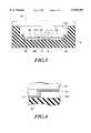
- FIG. 11is a section partially showing a conventional ceramic package and a SAW filter mounted thereon.
- FIG. 11a conventional ceramic package for encapsulating a surface acoustic wave (SAW) filter, shown in FIG. 11.
- the packagegenerally designated with a reference numeral 1
- a SAW filter chip or wafer chip 3is affixed to the package 1 by, e.g., adhesive 5 with its surface 4 carrying a pattern of electrodes facing upward.
- the electrode pattern, i.e., electrodes 6are connected to the pads 2 of the package 1 by bonding wires 7.
- a lid, not shown,is mounted on the top of the package 1 and sealed by solder.
- the electrodes 6are printed on a substrate of piezoelectric substance such as LiTaO 3 .
- the problem with the afore-mentioned conventional package 1is that the adjustment of impedance is extensively difficult partly because, on one hand, the patterned surface 4 is hermetically sealed in the package 1 and, on the other hand, partly because the electrode pattern itself is printed on LiTaO 3 or similar fragile material, as stated earlier.
- the packageAs shown in FIG. 1A, the package, generally designated with a reference numeral 10, is generally of a rectangular box shape.
- the package 10includes an input terminal 11, an output terminal 12, and four ground terminals 13-16 formed in a recess 10C cut therein.
- the ground terminalsare to be connected to ground.
- the output terminal 12 and ground terminals 15 and 16are respectively connected to terminal pads 12A, 15A and 16A, which are formed on one or front side face 10A of the package 10.
- the input terminal 11 and ground terminals 13 and 14Aare respectively connected to other terminal pads 11A, 13A and 14, which are also formed on another side, or rear face 10B of the package 10 opposite to the front side face 10A.
- a generally rectangular pad 17is formed of metal and positioned on the generally flat bottom 10D of the recess 10C (see FIG. 3) formed in the package 10.
- the metal pad 17is surrounded by the input terminal 11, output terminal 12, and ground terminals 13-16 as depicted. It is to be noted that the pad 17 may be provided with any desired shape and may be located at any desired position on the bottom surface 10D of the package 10 shown in FIG. 1A.
- a SAW filter chip 31 and bumps 32 to which the filter chip 31 is connectedare indicated by phantom lines. How to support the chip 31 by the bumps 32 will be described later.
- FIG. 2shows an alternative embodiment of the present invention.
- the structural elements like those shown in FIGS. 1A, 1B and 1Care designated by the same reference numerals, and a detailed description thereof will not be made in order to avoid redundancy.
- this embodimentmay be the same as what is shown in and described with reference to FIGS. 1A, 1B and 1C except that with the FIG. 2 embodiment the metal pad 17 is connected to the ground terminals 13-16 by connections, such as wires or metal strips, 18-21, respectively.
- the filter chip 31is mounted to the package 10 face down, i.e., with one of its primary surface 31A carrying electrode patterns 33 facing downward in the figure.
- the filter chip 31is connected to the bottom surface 10D of the package 10 by the bumps 32.
- the package 10includes a shoulder 34 for forming an appropriate air gap between the electrode pattern or propagation paths 33 of the filter chip 31 and the pad 17 of the package 10.
- the shoulder 34has a height, as measured from the bottom 10D of the recess 10C formed in the package 10, so selected as not to affect the connection using the bumps 32.
- the electrode pattern or propagation paths 33are printed on the primary surface 31A of the chip 31 in the form of metal, comb-like strips, for example, which are adapted to propagate surface acoustic waves over the surface of the piezoelectric substrate 31 along the paths 33.
- a lidshown with a phantom line 50, FIG. 3, is fitted on the top of the recess 10C of the package 10 in order to seal the package 10.
- a capacitance Cis produced between the propagation paths 33 of the filter chip 31 and the pad 17 of the package 10 due to the above-mentioned gap.
- a capacitance or capacitancescan be added, as shown in FIG. 6, 7 or 8. Specifically, a capacitance C 1 (FIG. 6), a capacitance C 2 (FIG. 7) or capacitances C 3 -C 11 (FIG.
- FIG. 8The application shown in FIG. 8 is of a maximum number of capacitances available with this specific circuit configuration. With the FIG. 8 application, the capacitances C 3 , C 4 , C 5 , C 7 , C 8 , C 9 and C 11 are inserted in serial to the propagation paths 33. The remaining capacitances C 6 , and C 10 have one electrodes thereof grounded, established by grounding metal pads 17 by connection wires 18, 19, 20 and 21 to the ground terminal 12, 14, 15 and 16, as shown in FIG. 2.
- a capacitance C 12can be added in a parallel connection.
- capacitances C 13 , C 14 and C 15may be added in a plurality of parallel connections.
- the capacitance or capacitancesallow the impedance of the SAW filter encapsulated in the package to be varied and thereby allow the frequency of the filter to appropriately be adjusted.
- the patterned surface of the filter chip 31faces downward, namely directed to the bottom 10D, it is protected from solder which may fly in the event of sealing of the package.
- the present inventionprovides a ceramic package for encapsulating a SAW filter and having various unprecedented advantages, as follows. Because the package includes a metal pad, a capacitance can be varied with ease on the basis of the shape of the pad. As a result, the impedance and phase of propagation paths can be varied, as desired. Further, bumps allow a SAW filter chip to be readily mounted to the package and reduce the cost of the package. Moreover, a shoulder formed in the recess of the package and surrounding the filter chip further promotes easy mounting of the chip and implements automated production. In addition, the capacitance added, to the packaged SAW filter varies the impedance and thereby allows the frequency of the SAW filter to be adjusted.
Landscapes
- Physics & Mathematics (AREA)
- Acoustics & Sound (AREA)
- Surface Acoustic Wave Elements And Circuit Networks Thereof (AREA)
Abstract
Description
Claims (7)
Applications Claiming Priority (2)
| Application Number | Priority Date | Filing Date | Title |
|---|---|---|---|
| JP8041194AJPH09232904A (en) | 1996-02-28 | 1996-02-28 | Ceramic package for saw filter |
| JP8-041194 | 1996-02-28 |
Publications (1)
| Publication Number | Publication Date |
|---|---|
| US5949305Atrue US5949305A (en) | 1999-09-07 |
Family
ID=12601622
Family Applications (1)
| Application Number | Title | Priority Date | Filing Date |
|---|---|---|---|
| US08/798,165Expired - LifetimeUS5949305A (en) | 1996-02-28 | 1997-02-10 | Saw filter encapsulated in a ceramic package with capacitance incorporated therein |
Country Status (5)
| Country | Link |
|---|---|
| US (1) | US5949305A (en) |
| EP (2) | EP1653613B1 (en) |
| JP (1) | JPH09232904A (en) |
| KR (1) | KR100326904B1 (en) |
| DE (1) | DE69738146T2 (en) |
Cited By (7)
| Publication number | Priority date | Publication date | Assignee | Title |
|---|---|---|---|---|
| US6252778B1 (en)* | 1997-10-23 | 2001-06-26 | Murata Manufacturing Co., Ltd. | Complex electronic component |
| US6339365B1 (en)* | 1998-12-29 | 2002-01-15 | Kabushiki Kaisha Toshiba | Surface acoustic wave device comprising first and second chips face down bonded to a common package ground |
| US9006880B1 (en) | 2000-11-28 | 2015-04-14 | Knowles Electronics, Llc | Top port multi-part surface mount silicon condenser microphone |
| US9040360B1 (en) | 2000-11-28 | 2015-05-26 | Knowles Electronics, Llc | Methods of manufacture of bottom port multi-part surface mount MEMS microphones |
| US9078063B2 (en) | 2012-08-10 | 2015-07-07 | Knowles Electronics, Llc | Microphone assembly with barrier to prevent contaminant infiltration |
| US9374643B2 (en) | 2011-11-04 | 2016-06-21 | Knowles Electronics, Llc | Embedded dielectric as a barrier in an acoustic device and method of manufacture |
| US9794661B2 (en) | 2015-08-07 | 2017-10-17 | Knowles Electronics, Llc | Ingress protection for reducing particle infiltration into acoustic chamber of a MEMS microphone package |
Families Citing this family (10)
| Publication number | Priority date | Publication date | Assignee | Title |
|---|---|---|---|---|
| DE69938989D1 (en) | 1998-05-29 | 2008-08-14 | Fujitsu Ltd | Acoustic surface acoustic wave filter with improved suppression outside of a passband |
| JP3726998B2 (en)* | 1999-04-01 | 2005-12-14 | 株式会社村田製作所 | Surface wave device |
| JP3860364B2 (en)* | 1999-08-11 | 2006-12-20 | 富士通メディアデバイス株式会社 | Surface acoustic wave device |
| KR100483042B1 (en)* | 2000-11-29 | 2005-04-15 | 삼성전기주식회사 | Method and device for sealing ceramic package of saw filter |
| KR100716155B1 (en)* | 2001-03-08 | 2007-05-10 | 엘지이노텍 주식회사 | Surface acoustic wave filter package with matching circuit |
| KR100519750B1 (en)* | 2001-05-10 | 2005-10-07 | 삼성전자주식회사 | Chip scale packaging structure sealed with low temperature Co-fired ceramic and the method thereof |
| KR20030065950A (en)* | 2002-02-02 | 2003-08-09 | 보성반도체 주식회사 | a manufacture method of super slim ceramic package with metalic bump |
| KR100435042B1 (en)* | 2002-04-27 | 2004-06-07 | 엘지이노텍 주식회사 | Method for duplexer package |
| KR100455699B1 (en)* | 2002-10-09 | 2004-11-06 | 주식회사 케이이씨 | surface acoustic wave filter device |
| US10483248B2 (en)* | 2017-03-23 | 2019-11-19 | Skyworks Solutions, Inc. | Wafer level chip scale filter packaging using semiconductor wafers with through wafer vias |
Citations (11)
| Publication number | Priority date | Publication date | Assignee | Title |
|---|---|---|---|---|
| EP0472856A2 (en)* | 1990-07-02 | 1992-03-04 | Japan Radio Co., Ltd | Surface acoustic wave device and its manufacturing method |
| JPH04360407A (en)* | 1991-06-07 | 1992-12-14 | Matsushita Electric Ind Co Ltd | Ceramic package for surface wave device |
| EP0527468A1 (en)* | 1991-08-12 | 1993-02-17 | Hitachi, Ltd. | High frequency module |
| JPH0590873A (en)* | 1991-09-28 | 1993-04-09 | Murata Mfg Co Ltd | Surface acoustic wave device |
| JPH05335878A (en)* | 1992-05-29 | 1993-12-17 | Meidensha Corp | Surface installation type surface acoustic wave element |
| US5281883A (en)* | 1990-11-05 | 1994-01-25 | Fujitsu Limited | Surface acoustic wave device with improved junction bonding and package miniaturization |
| JPH0697759A (en)* | 1992-09-16 | 1994-04-08 | Fujitsu Ltd | Surface acoustic wave device and its manufacture |
| EP0637871A1 (en)* | 1993-08-06 | 1995-02-08 | Matsushita Electric Industrial Co., Ltd. | Surface acoustic wave device mounted module |
| JPH07212180A (en)* | 1994-01-10 | 1995-08-11 | Toyo Commun Equip Co Ltd | Surface mounted piezoelectric parts |
| JPH07336183A (en)* | 1994-06-03 | 1995-12-22 | Japan Energy Corp | Surface acoustic wave device |
| US5699027A (en)* | 1995-03-28 | 1997-12-16 | Matsushita Electric Industrial Co., Ltd. | Surface acoustic wave devices having a guard layer |
- 1996
- 1996-02-28JPJP8041194Apatent/JPH09232904A/ennot_activeWithdrawn
- 1997
- 1997-02-07EPEP05110513Apatent/EP1653613B1/ennot_activeExpired - Lifetime
- 1997-02-07EPEP97300812Apatent/EP0793340A3/ennot_activeCeased
- 1997-02-07DEDE69738146Tpatent/DE69738146T2/ennot_activeExpired - Lifetime
- 1997-02-10USUS08/798,165patent/US5949305A/ennot_activeExpired - Lifetime
- 1997-02-12KRKR1019970004103Apatent/KR100326904B1/ennot_activeExpired - Lifetime
Patent Citations (13)
| Publication number | Priority date | Publication date | Assignee | Title |
|---|---|---|---|---|
| EP0472856A2 (en)* | 1990-07-02 | 1992-03-04 | Japan Radio Co., Ltd | Surface acoustic wave device and its manufacturing method |
| US5252882A (en)* | 1990-07-02 | 1993-10-12 | Japan Radio Co., Ltd. | Surface acoustic wave device and its manufacturing method |
| US5281883A (en)* | 1990-11-05 | 1994-01-25 | Fujitsu Limited | Surface acoustic wave device with improved junction bonding and package miniaturization |
| JPH04360407A (en)* | 1991-06-07 | 1992-12-14 | Matsushita Electric Ind Co Ltd | Ceramic package for surface wave device |
| EP0527468A1 (en)* | 1991-08-12 | 1993-02-17 | Hitachi, Ltd. | High frequency module |
| JPH0590873A (en)* | 1991-09-28 | 1993-04-09 | Murata Mfg Co Ltd | Surface acoustic wave device |
| JPH05335878A (en)* | 1992-05-29 | 1993-12-17 | Meidensha Corp | Surface installation type surface acoustic wave element |
| JPH0697759A (en)* | 1992-09-16 | 1994-04-08 | Fujitsu Ltd | Surface acoustic wave device and its manufacture |
| EP0637871A1 (en)* | 1993-08-06 | 1995-02-08 | Matsushita Electric Industrial Co., Ltd. | Surface acoustic wave device mounted module |
| US5459368A (en)* | 1993-08-06 | 1995-10-17 | Matsushita Electric Industrial Co., Ltd. | Surface acoustic wave device mounted module |
| JPH07212180A (en)* | 1994-01-10 | 1995-08-11 | Toyo Commun Equip Co Ltd | Surface mounted piezoelectric parts |
| JPH07336183A (en)* | 1994-06-03 | 1995-12-22 | Japan Energy Corp | Surface acoustic wave device |
| US5699027A (en)* | 1995-03-28 | 1997-12-16 | Matsushita Electric Industrial Co., Ltd. | Surface acoustic wave devices having a guard layer |
Cited By (22)
| Publication number | Priority date | Publication date | Assignee | Title |
|---|---|---|---|---|
| US6252778B1 (en)* | 1997-10-23 | 2001-06-26 | Murata Manufacturing Co., Ltd. | Complex electronic component |
| US6339365B1 (en)* | 1998-12-29 | 2002-01-15 | Kabushiki Kaisha Toshiba | Surface acoustic wave device comprising first and second chips face down bonded to a common package ground |
| US9096423B1 (en) | 2000-11-28 | 2015-08-04 | Knowles Electronics, Llc | Methods of manufacture of top port multi-part surface mount MEMS microphones |
| US9133020B1 (en) | 2000-11-28 | 2015-09-15 | Knowles Electronics, Llc | Methods of manufacture of bottom port surface mount MEMS microphones |
| US9023689B1 (en) | 2000-11-28 | 2015-05-05 | Knowles Electronics, Llc | Top port multi-part surface mount MEMS microphone |
| US9040360B1 (en) | 2000-11-28 | 2015-05-26 | Knowles Electronics, Llc | Methods of manufacture of bottom port multi-part surface mount MEMS microphones |
| US9051171B1 (en) | 2000-11-28 | 2015-06-09 | Knowles Electronics, Llc | Bottom port surface mount MEMS microphone |
| US9061893B1 (en) | 2000-11-28 | 2015-06-23 | Knowles Electronics, Llc | Methods of manufacture of top port multi-part surface mount silicon condenser microphones |
| US9067780B1 (en) | 2000-11-28 | 2015-06-30 | Knowles Electronics, Llc | Methods of manufacture of top port surface mount MEMS microphones |
| US10321226B2 (en) | 2000-11-28 | 2019-06-11 | Knowles Electronics, Llc | Top port multi-part surface mount MEMS microphone |
| US9006880B1 (en) | 2000-11-28 | 2015-04-14 | Knowles Electronics, Llc | Top port multi-part surface mount silicon condenser microphone |
| US9024432B1 (en) | 2000-11-28 | 2015-05-05 | Knowles Electronics, Llc | Bottom port multi-part surface mount MEMS microphone |
| US9139421B1 (en) | 2000-11-28 | 2015-09-22 | Knowles Electronics, Llc | Top port surface mount MEMS microphone |
| US9139422B1 (en) | 2000-11-28 | 2015-09-22 | Knowles Electronics, Llc | Bottom port surface mount MEMS microphone |
| US9148731B1 (en) | 2000-11-28 | 2015-09-29 | Knowles Electronics, Llc | Top port surface mount MEMS microphone |
| US9150409B1 (en) | 2000-11-28 | 2015-10-06 | Knowles Electronics, Llc | Methods of manufacture of bottom port surface mount MEMS microphones |
| US9156684B1 (en) | 2000-11-28 | 2015-10-13 | Knowles Electronics, Llc | Methods of manufacture of top port surface mount MEMS microphones |
| US9338560B1 (en) | 2000-11-28 | 2016-05-10 | Knowles Electronics, Llc | Top port multi-part surface mount silicon condenser microphone |
| US9980038B2 (en) | 2000-11-28 | 2018-05-22 | Knowles Electronics, Llc | Top port multi-part surface mount silicon condenser microphone |
| US9374643B2 (en) | 2011-11-04 | 2016-06-21 | Knowles Electronics, Llc | Embedded dielectric as a barrier in an acoustic device and method of manufacture |
| US9078063B2 (en) | 2012-08-10 | 2015-07-07 | Knowles Electronics, Llc | Microphone assembly with barrier to prevent contaminant infiltration |
| US9794661B2 (en) | 2015-08-07 | 2017-10-17 | Knowles Electronics, Llc | Ingress protection for reducing particle infiltration into acoustic chamber of a MEMS microphone package |
Also Published As
| Publication number | Publication date |
|---|---|
| EP0793340A3 (en) | 1998-05-13 |
| KR970063919A (en) | 1997-09-12 |
| EP1653613B1 (en) | 2007-09-12 |
| JPH09232904A (en) | 1997-09-05 |
| EP1653613A1 (en) | 2006-05-03 |
| DE69738146T2 (en) | 2008-06-12 |
| DE69738146D1 (en) | 2007-10-25 |
| KR100326904B1 (en) | 2002-07-03 |
| EP0793340A2 (en) | 1997-09-03 |
Similar Documents
| Publication | Publication Date | Title |
|---|---|---|
| US5949305A (en) | Saw filter encapsulated in a ceramic package with capacitance incorporated therein | |
| US5939956A (en) | Multiple-mode piezoelectric filter with acoustic and electromagnetic separation between stages | |
| US6114635A (en) | Chip-scale electronic component package | |
| EP0485151B1 (en) | Surface acoustic wave device | |
| US6566981B2 (en) | Surface acoustic wave device having plural ground conductor films in the housing cavity | |
| US7095161B2 (en) | Piezoelectric resonator | |
| US6329739B1 (en) | Surface-acoustic-wave device package and method for fabricating the same | |
| JPH04293310A (en) | Surface acoustic wave device | |
| US20200044623A1 (en) | Piezoelectric resonator device | |
| US4430596A (en) | Temperature insensitive piezoelectric crystal mounting arrangement | |
| EP0859465B1 (en) | Surface mounting piezoelectric filter | |
| JP4724519B2 (en) | Piezoelectric oscillator | |
| JP2002026656A (en) | SAW oscillator | |
| JP4724518B2 (en) | Piezoelectric oscillator | |
| JP3389530B2 (en) | Semiconductor device | |
| JPH0653775A (en) | Surface acoustic wave device | |
| JPH10215143A (en) | Surface acoustic wave device | |
| JP2762974B2 (en) | Semiconductor container | |
| KR100368607B1 (en) | semiconductor package | |
| KR20060115531A (en) | Surface acoustic wave device package with excellent airtightness and manufacturing method | |
| JP2007300173A (en) | Package for electronic device, and electronic device | |
| JP2004179832A (en) | Structure of multimode piezoelectric filter | |
| JP3736226B2 (en) | SAW device | |
| JP3317926B2 (en) | Surface acoustic wave device | |
| KR100489825B1 (en) | Flip chip type surface acoustic wave apparatus |
Legal Events
| Date | Code | Title | Description |
|---|---|---|---|
| AS | Assignment | Owner name:OKI ELECTRIC INDUSTRY CO., LTD., JAPAN Free format text:ASSIGNMENT OF ASSIGNORS INTEREST;ASSIGNOR:SHIMAMURA, HAJIME;REEL/FRAME:008582/0759 Effective date:19970124 | |
| STCF | Information on status: patent grant | Free format text:PATENTED CASE | |
| FEPP | Fee payment procedure | Free format text:PAYOR NUMBER ASSIGNED (ORIGINAL EVENT CODE: ASPN); ENTITY STATUS OF PATENT OWNER: LARGE ENTITY | |
| FPAY | Fee payment | Year of fee payment:4 | |
| FPAY | Fee payment | Year of fee payment:8 | |
| AS | Assignment | Owner name:OKI SEMICONDUCTOR CO., LTD., JAPAN Free format text:CHANGE OF NAME;ASSIGNOR:OKI ELECTRIC INDUSTRY CO., LTD.;REEL/FRAME:022288/0277 Effective date:20081001 | |
| FPAY | Fee payment | Year of fee payment:12 | |
| FEPP | Fee payment procedure | Free format text:PAYOR NUMBER ASSIGNED (ORIGINAL EVENT CODE: ASPN); ENTITY STATUS OF PATENT OWNER: LARGE ENTITY Free format text:PAYER NUMBER DE-ASSIGNED (ORIGINAL EVENT CODE: RMPN); ENTITY STATUS OF PATENT OWNER: LARGE ENTITY | |
| AS | Assignment | Owner name:LAPIS SEMICONDUCTOR CO., LTD., JAPAN Free format text:CHANGE OF NAME;ASSIGNOR:OKI SEMICONDUCTOR CO., LTD.;REEL/FRAME:027622/0360 Effective date:20111001 | |
| AS | Assignment | Owner name:INTELLECTUAL VENTURES FUND 77 LLC, NEVADA Free format text:ASSIGNMENT OF ASSIGNORS INTEREST;ASSIGNOR:LAPIS SEMICONDUCTOR CO., LTD.;REEL/FRAME:028093/0534 Effective date:20120302 | |
| AS | Assignment | Owner name:INTELLECTUAL VENTURES HOLDING 81 LLC, NEVADA Free format text:MERGER;ASSIGNOR:INTELLECTUAL VENTURES FUND 77 LLC;REEL/FRAME:037577/0581 Effective date:20150827 | |
| AS | Assignment | Owner name:HANGER SOLUTIONS, LLC, GEORGIA Free format text:ASSIGNMENT OF ASSIGNORS INTEREST;ASSIGNOR:INTELLECTUAL VENTURES ASSETS 158 LLC;REEL/FRAME:051486/0425 Effective date:20191206 | |
| AS | Assignment | Owner name:INTELLECTUAL VENTURES ASSETS 158 LLC, DELAWARE Free format text:ASSIGNMENT OF ASSIGNORS INTEREST;ASSIGNOR:INTELLECTUAL VENTURES HOLDING 81 LLC;REEL/FRAME:051777/0017 Effective date:20191126 |