US5949264A - Digital phase detector and charge pump system reset and balanced current source matching methods and systems - Google Patents
Digital phase detector and charge pump system reset and balanced current source matching methods and systemsDownload PDFInfo
- Publication number
- US5949264A US5949264AUS08/758,529US75852996AUS5949264AUS 5949264 AUS5949264 AUS 5949264AUS 75852996 AUS75852996 AUS 75852996AUS 5949264 AUS5949264 AUS 5949264A
- Authority
- US
- United States
- Prior art keywords
- output
- charge pump
- node
- circuit
- nodes
- Prior art date
- Legal status (The legal status is an assumption and is not a legal conclusion. Google has not performed a legal analysis and makes no representation as to the accuracy of the status listed.)
- Expired - Lifetime
Links
Images


Classifications
- H—ELECTRICITY
- H03—ELECTRONIC CIRCUITRY
- H03L—AUTOMATIC CONTROL, STARTING, SYNCHRONISATION OR STABILISATION OF GENERATORS OF ELECTRONIC OSCILLATIONS OR PULSES
- H03L7/00—Automatic control of frequency or phase; Synchronisation
- H03L7/06—Automatic control of frequency or phase; Synchronisation using a reference signal applied to a frequency- or phase-locked loop
- H03L7/08—Details of the phase-locked loop
- H03L7/085—Details of the phase-locked loop concerning mainly the frequency- or phase-detection arrangement including the filtering or amplification of its output signal
- H03L7/089—Details of the phase-locked loop concerning mainly the frequency- or phase-detection arrangement including the filtering or amplification of its output signal the phase or frequency detector generating up-down pulses
- H03L7/0891—Details of the phase-locked loop concerning mainly the frequency- or phase-detection arrangement including the filtering or amplification of its output signal the phase or frequency detector generating up-down pulses the up-down pulses controlling source and sink current generators, e.g. a charge pump
- H03L7/0895—Details of the current generators
- H—ELECTRICITY
- H03—ELECTRONIC CIRCUITRY
- H03D—DEMODULATION OR TRANSFERENCE OF MODULATION FROM ONE CARRIER TO ANOTHER
- H03D13/00—Circuits for comparing the phase or frequency of two mutually-independent oscillations
- H03D13/003—Circuits for comparing the phase or frequency of two mutually-independent oscillations in which both oscillations are converted by logic means into pulses which are applied to filtering or integrating means
- H03D13/004—Circuits for comparing the phase or frequency of two mutually-independent oscillations in which both oscillations are converted by logic means into pulses which are applied to filtering or integrating means the logic means delivering pulses at more than one terminal, e.g. up and down pulses
- H—ELECTRICITY
- H03—ELECTRONIC CIRCUITRY
- H03L—AUTOMATIC CONTROL, STARTING, SYNCHRONISATION OR STABILISATION OF GENERATORS OF ELECTRONIC OSCILLATIONS OR PULSES
- H03L7/00—Automatic control of frequency or phase; Synchronisation
- H03L7/06—Automatic control of frequency or phase; Synchronisation using a reference signal applied to a frequency- or phase-locked loop
- H03L7/08—Details of the phase-locked loop
- H03L7/085—Details of the phase-locked loop concerning mainly the frequency- or phase-detection arrangement including the filtering or amplification of its output signal
- H03L7/089—Details of the phase-locked loop concerning mainly the frequency- or phase-detection arrangement including the filtering or amplification of its output signal the phase or frequency detector generating up-down pulses
- H03L7/0891—Details of the phase-locked loop concerning mainly the frequency- or phase-detection arrangement including the filtering or amplification of its output signal the phase or frequency detector generating up-down pulses the up-down pulses controlling source and sink current generators, e.g. a charge pump
- H03L7/0893—Details of the phase-locked loop concerning mainly the frequency- or phase-detection arrangement including the filtering or amplification of its output signal the phase or frequency detector generating up-down pulses the up-down pulses controlling source and sink current generators, e.g. a charge pump the up-down pulses controlling at least two source current generators or at least two sink current generators connected to different points in the loop
Definitions
- the technical field of the present inventionis digital phase detection and charge pumping methods and systems, and more particularly charge reset and balanced current source matching methods and systems for digital phase detection and charge pump systems.
- a delay circuitis incorporated in the digital phase detector to provide a fixed delay time.
- the delay circuitis hampered by dependency upon temperature and device process variations. This causes excessive delay times in some instances, and insufficient time delays at other times, degrading digital phase detector performance.
- Such fixed time delaysare further additionally subject to noise in part attributable to the magnitude of digital phase detector deadband.
- output signalsmay vary undesireably as a result of current variations in p-channel and n-channel portions of the charge pump system.
- a digital phase detector and charge pump circuit systemincludes charging and discharging sensing circuitry which resets the digital phase detector according to the charge outputs between the charge pump circuits and a following loop filter.
- a digital phase detector and charge pump circuitincludes a tri-state digital phase detector, a charge pump, and charge reset circuitry including a reset control switch responsive to both up and down outputs of the phase detector.
- the charge pump circuitconverts the tri-state outputs of the digital phase detector into charging or discharging or high-impedance output states of a following low-pass loop filter for controlling voltage-controlled oscillator (VCO) output frequency.
- VCOvoltage-controlled oscillator
- the charge reset circuitryincludes charging sensing and discharging sensing circuitry which emulates the charge pump circuit to determine appropriate delay times for reset operation.
- a capacitor in the charging sensing circuitis reset to ground by a controlled switch.
- the UP output of the digital phase detectorgoes high, it turns on the source current of the charge pump circuit to charge the loop filter. In this state, the controlled switch is off and the charging sensing circuit emulates charge pump charging behavior.
- the DOWN output of the digital phase detectorgoes low, the capacitor in the discharging sensing circuit is charged to VCC.
- the DOWN output of the digital phase detectorgoes high, the capacitor discharges to emulate the corresponding discharging behavior of the charge pump circuit.
- a resistor in the charging and discharging circuitryadds another flexibility to adjust the circuit time constant to emulate actual time requirements of a capacitor in the loop filter.
- the sensing capacitors in the charging and discharging circuitry according to the present inventionare much smaller than the loop filter capacitor.
- the current sources to charge and discharge the sensing capacitorsand have smaller than the sinking and sourcing current sources associated with the charge pump circuitry according to the present invention.
- the output from the charging and discharging circuitryis fed into a logic control circuit to reset the digital phase detector when both UP and DOWN outputs are set to logical high.
- a digital phase detector and charge pump systemincludes charging and discharging sensing circuitry which resets the digital phase detector with a reduced deadband VCO frequency range in which the digital phase detector and charge pump are not activated.
- the reduced deadband timeis achieved by emulating the charging and discharging action of the charge pump circuitry to provide appropriate delay time to reset the digital phase detector.
- a charge pump systememploys current mirror transistor combinations which alternate between n-channel and p-channel devices to reduce the impact of undesired variation in p-channel and n-channel current carrying levels.
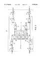
- FIG. 1Ais a diagram of a digital phase detector and charge pump circuit charge reset system according to the present invention.
- FIG. 1Bis a timing diagram showing the operation of a digital phase detector and charge pump circuit charge reset system according to the present invention
- FIG. 2is a diagram of a charge pump circuit according to the present invention.
- FIG. 3is a diagram of a phase comparator circuit according to the present invention, broken into two parts, FIG. 3a and FIG. 3b for ease of viewing.
- FIG. 1Ais a diagram of digital circuitry for a phase detector and charge pump circuit charge reset system 2 according to the present invention. More particularly, FIG. 1A shows phase detector and charge pump circuit charge reset system for producing output voltage controlled oscillator (VCO) signal levels based upon an input frequency signal, PHU, and a reference signal, PHD.
- Phase detector and charge pump circuit charge reset system 2includes a phase comparator circuit 3, a charge pump circuit 4, first and second respective current sources 5a and 5b (i.e., sourcing and sinking current sources, respectively), a loop filter circuit comprising a capacitor 6 to ground according to one embodiment, a VCO output 7, and a reset circuit 8 according to the present invention.
- Phase comparator circuit 3is a tri-state digital phase detector which receives a reference signal (PHU) and an input frequency signal (PHD) and produces UP and DOWN output signals on first and second respective output connections 3a and 3b, serving as respective inputs to charge pump circuit 4.
- PHUreference signal
- PLDinput frequency signal
- U. L. Rohdedescribes tri-state digital phase detectors which can be employed in connection with the present invention in "Digital PLL Frequency Synthesizer Theory and Design" published in 1983 by Prentice Hall of Englewood Cliffs, N.Y.
- Charge pump Circuit 4responds to UP and DOWN signals from phase comparator circuit 3 by providing output signals on output connectors 4a and 4b to activate respective sourcing and sinking current sources 5a and 5b.
- Current sources 5a and 5bare connected in series between VCC and ground, at a common node 5a' to which a loop filter circuit, comprising, according to one embodiment, a capacitor 6, is connected.
- An output signal on connection 4a from charge pump circuit 4sources current to loop filter capacitor 6 from VCC to VCO output 7.
- An output signal from charge pump circuit 4 on connection 4bsinks current from loop filter capacitor 6 to ground.
- Reset circuit 8is connected to first and second output connections 4a and 4b of charge pump circuit 4 and provides a reset output signal to phase comparator circuit 3 as will be discussed below.
- Charge reset circuit 8particularly includes a discharging circuit 8a, a charging circuit 8b, a discharging switch 9a connected between VCC and discharging circuit 8a, and a charging switch 9b connected between charging circuit 8b and ground.
- Charge reset circuit 8further includes a control invertor 9a' for opening and closing discharging switch 9a based upon the logical state of DOWN signals on down connection 3b from phase comparator 3, a control invertor 9b' for opening and closing charging switch 9b based upon the logical state of UP signals on up connection 3a from phase comparator 3, an inverter 9b" connected to charging circuit 8b, and a NOR gate 9a" having first and second input connections connected respectively to discharging circuit 8a and to inverter 9b".
- NOR gate 9a"further includes an output connection connected to phase comparator 3 for providing reset signals thereto.
- Discharging circuit 8aincludes a current source 18a, a sensing capacitor 18b, and a resistor 18c.
- Charging circuit 8bincludes a current source 19a, a sensing capacitor 19b, and a resistor 19c.
- Current source 18a of discharging circuit 8ais connected to ground in parallel with resistor 18c and sensing capacitor 18c.
- Current source 19a of charging circuit 8bis connected in series with resistor 19c and sensing capacitor 19b between VCC and ground.
- Charge reset circuit 8receives first and second inputs from charge pump 4 at respective output connections 4a and 4b in order to sense the logical state of signals applied thereupon by charge pump 4.
- a first input of charge reset circuit 8which is connected to output connection 4a activates current source 18 when a sufficient output level signal from charge pump 4 is received as a DOWN signal at output connection 4b.
- the effect of activating current source 18ais to discharge sensing capacitor 18b through resistor 18a according to an RC time constant determined by the capacitance of sensing capacitor 18b and the resistance of resistor 18c. Resistor 18c and capacitor 18b are connected at an output node of discharging circuit 8a. When sensing capacitor 18b is discharged, the output node of discharging circuit 8a produces a zero logical value voltage level input for NOR gate element 9a".
- the same output nodeproduces a positive voltage level corresponding to a one (1) logical value input at NOR gate element 9a", when switch 9a is closed to connect the node to VCC.
- Such switch closure for switch 9ais produced in inverted form by a DOWN signal at connection 3b between phase comparator 3 and charge pump 4.
- a DOWN signal or pulse on connection 3bwill produce a zero switch control signal at switch 9a, closing switch 9a to apply a logical one (1) at the input of NOR gate element 9a".
- the same DOWN signal at connection 3bwill at a delayed time be reflected by an UP output pulse original at output connection 4b from charge pump 4.
- This pulsewill activate current source 19a, charging sensing capacitor 19b through resistor 19c at a rate which is a function of the product of the capacitance of sensing capacitor 19b and the resistance of resistor 19c.
- sensing capacitor 19bwill produce a logical one input signal at the input of invertor 9b" and a corresponding logical zero input at the other of the inputs to NOR gate element 9a".
- Control switches 9a and 9bprevent reset by NOR gate element 9a" unless the respective logical states of UP and DOWN signals at connections 3a and 3b are both high.
- FIG. 1bis a timing diagram showing the operation of digital phase detector and charge pump circuit charge reset system 2 according to the present invention.
- FIG. 1Bshows UP and DOWN signal pulses of indicated terms at the outputs of phase comparator 3 produced by to corresponding UP and DOWN signals PHU and PHD provided as inputs of phase comparator 3. Three reset examples are shown, i.e., RESET, RESET', and RESET".
- Phase comparator 3has input signal PHU and PHD as shown, which correspond to output UP and DOWN signals for input to charge pump 4.
- the rising edge of the PHU inputinitiates UP pulse at the output of phase comparator 3.
- each PHD pulse rising edgegenerates a corresponding DOWN pulse at the phase comparator output.
- a reset signalis provided to phase comparator 3 whenever the second one of PHU and PHD goes up. After a time “delay" characteristic of the electric circuitry used, both UP and DOWN go to logical zero responsive to reset. If PHD goes high while UP is high, reset occurs. Further, if PHU is high and DOWN goes high, reset occurs. RESET and RESET' occur with PHU going high first after reset, while RESET" occurs with PHD going high first.
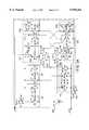
- FIG. 2is a circuit diagram of a phase comparator 20 according to one embodiment of the present invention.
- Phase comparator 20is reset along a RESET line provided from reset circuit 8 shown in FIG. 1A.
- Phase comparator 20includes input inverters 21 and 22 respectively receiving signal inputs PHU and PHD, i.e., phase UP and phase DOWN input signals.
- Phase comparator 3further includes NAND gates 23 and 24 respectively connected to the outputs of inverters 21 and 22.
- Phase detector 3further includes a bank of NAND gates 25a, 25b, 25c, and 25d, each of which has first and second inputs, and an output. The inputs of NAND gates 25a and 25d are respectively connected to the respective outputs of NAND gates 23 and 24.
- Phase detector 3further includes NAND gates 27, 28, 29 and 30, each of which has first, second, and third inputs, and an output.
- the respective outputs of NAND gates 27 and 28are connected to each other and to the respective inputs of NAND gates 25b and 25c.
- the respective outputs of NAND gates 25a and 25dare connected to first inputs of NAND gates 27, 28, 29 and 30.
- the respective outputs of NAND gates 23 and 24are connected to respective second inputs of NAND gates 29 and 30.
- a reset signal inputis respectively connected to the third inputs of NAND gates 27 and 28.
- Phase detector 3finally includes inverters 31 and 32 connected at the outputs respectively of NAND gates 29 and 30 to produce output UP and DOWN signals.
- the circuitry of FIG. 2operates in accordance with the timing diagram of FIG. 1B.
- FIG. 3is a diagram of a charge pump circuit 400 according to the present invention, broken into two parts, FIG. 3A and FIG. 3B for ease of viewing.
- FIGS. 3Aparticularly shows a first portion of charge pump circuit 400 according to an embodiment of the present invention, including input inverters 40a and 40b connected to respective input signals UP and DOWN.
- Charge pump circuit 400further includes a current source 41 for driving a transistor circuit including transistors 42, 43, 44, 45, 46, 47 and 48 in successive cascading current mirror arrangements. More particularly, transistor 42 is connected in series with current source 42. Transistor 43 is connected in series with transistor 44 to produce a four-fold current increase by action of a current mirror 142 comprising transistors 42 and 43.
- Transistor 46is connected in series with transistor 45, ensuring the same level of current in transistor 46 as in 44 and 45, based upon action of current mirror 144 comprising transistors 44, 45, and 48.
- Transistor 47is connected in series with transistor 50a through a transmission gate comprising transistors 49a and 49b' at a four fold current increase over series connected transistors 46 and 45 by action of current mirror 146 comprising gate connected transistors 46 and 47.
- transistors 48 and 50a'are connected in series through a transmission gate comprising transistors 49a' and 49b' ensuring a four-fold increase in electric current in transistors 48 and 50a' over the current level in transistor 44 by action of current mirror 144 acting through transistors 44 and 48 thereof.
- Transistors 42 and 43; transistors 44, 45 and 48; and transistors 46 and 47are each gate connected.
- the gates of transistors 42 and 43are connected to the drain of P-channel transistor 42; the gates of transistors 46 and 47, to the drain of P-channel transistor 46; and the gates of transistors 44, 45 and 48 to the drain of transistor 44.
- the current through transistors 47 and 48is a selected increased function of the current from current source 41 which passes through transistor 42.
- the current through transistors 43 and 44is a selected increased function of the current through transistor 42; and the current through transistors 46 and 48 is a selected other function of the current through transistor 44.
- Charge pump circuit 400further includes transistors 49a, 49a', 49b, 49b', 50a, 50a', 50b, 50b', 41, 51', 52, 52', 53, and 53'.
- Transistors 49a' and 49b' and transistors 49a and 49bare each connected as transfer gates.
- Transistors 51' and 52'are connected in series to carry a current which is sixteen times the current in transistor 50a', based upon operation of a current mirror 151 comprising transistors 50a', 51', and 50b'.
- Transistors 51 and 52are connected in series to carry a current which is sixteen times the current in transistor 50a, based upon operation of a current mirror 150 comprising transistors 50a, 50b, and 51.
- FIG. 3Bis an extension of FIG.
- charge pump circuit 400is connected to current source transistors 54 and 54' in turn connected to each other at node 54" which leads to a loop filter, capacitor (not shown).
- Transistor 54 in FIG. 3Bis connected to node 54" to generate 64 times the current level passing through transistor 53 in FIG. 3A of a current mirror arrangement 153A and 153B, including transistors 52, 53, and 54 (in FIG. 3B).
- Transistor 54'is connected to node 54" to generate 64 times the current level passing through transistor 53' in FIG. 3A of a current mirror arrangement 152a and 152b, including transistors 53', 52', and 54' (in FIG. 3B).
- Transistors 49a and 49b and transistors 49a' and 49b'are each respectively connected in parallel as transfer gates.
- Transistors 50b', the transfer gate combination of transistors 49a' and 49b', and transistor 48are connected in series.
- Transistors 50b, the transfer gate combination of transistors 49a and 49b', and 47are connected in series.
- Transistors 50a' and 50b' and transistors 50a and 50bare each respectively connected in series with each other.
- Transistors 51' and 52' and transistor 52 and 51are each respectively connected to each other in series.
- Transistors 52 and 53 and transistors 52' and 53'are respectively each connected in parallel.
- Current source transistors 54 and 54', transistors 55 and 57, and transistors 57' and 55' of reset circuit 108,are each respectively connected in series.
- Respective resistors 56 and 56'are connected in series between respective transistors 55 and 57, and transistors 57' and 55'.
- Transistors 58' and 58provide respective capacitances to VDD and ground.
- the mode between transistor 57' and resistor 56'i.e., node A
- the mode between transistor 57' and resistor 56'i.e., node A
- the mode between transistor 57' and resistor 56'i.e., node A
- the mode between transistor 57' and resistor 56'i.e., node A
- NOR gate 60is connected to transistor 58; and a first input to
- the node between resistor 56 and transistor 57(i.e., node B) is in turn connected to transistor 58 and the input of inverter 59 which in turn is connected to the remaining input of NOR gate 60 which provides an output RESET signal.
- Transistors 58 and 58'are connected as capacitors.
- electric current from current source 41is mirror multiplied by a p-channel current mirror 142 connected to an n-channel current mirror 144 in turn connected to a p-channel current mirror 146.
- An input UP signal in FIG. 3Aopens transfer gate 49a and 49b, engaging p-channel current mirror 146 with n-channel current mirror 150 which in turn engages p-channel current mirror 153a including current source transistor 54.
- a DOWN signalopens transfer gate 49a; and 49b', engaging n-channel current mirror 144 with n-channel current mirror.
Landscapes
- Engineering & Computer Science (AREA)
- Power Engineering (AREA)
- Stabilization Of Oscillater, Synchronisation, Frequency Synthesizers (AREA)
Abstract
Description
Claims (8)
Priority Applications (2)
| Application Number | Priority Date | Filing Date | Title |
|---|---|---|---|
| US08/758,529US5949264A (en) | 1996-11-29 | 1996-11-29 | Digital phase detector and charge pump system reset and balanced current source matching methods and systems |
| US09/339,435US6140853A (en) | 1996-11-29 | 1999-06-24 | Digital phase detector and charge pump system reset and balanced current source matching |
Applications Claiming Priority (1)
| Application Number | Priority Date | Filing Date | Title |
|---|---|---|---|
| US08/758,529US5949264A (en) | 1996-11-29 | 1996-11-29 | Digital phase detector and charge pump system reset and balanced current source matching methods and systems |
Related Child Applications (1)
| Application Number | Title | Priority Date | Filing Date |
|---|---|---|---|
| US09/339,435DivisionUS6140853A (en) | 1996-11-29 | 1999-06-24 | Digital phase detector and charge pump system reset and balanced current source matching |
Publications (1)
| Publication Number | Publication Date |
|---|---|
| US5949264Atrue US5949264A (en) | 1999-09-07 |
Family
ID=25052066
Family Applications (2)
| Application Number | Title | Priority Date | Filing Date |
|---|---|---|---|
| US08/758,529Expired - LifetimeUS5949264A (en) | 1996-11-29 | 1996-11-29 | Digital phase detector and charge pump system reset and balanced current source matching methods and systems |
| US09/339,435Expired - LifetimeUS6140853A (en) | 1996-11-29 | 1999-06-24 | Digital phase detector and charge pump system reset and balanced current source matching |
Family Applications After (1)
| Application Number | Title | Priority Date | Filing Date |
|---|---|---|---|
| US09/339,435Expired - LifetimeUS6140853A (en) | 1996-11-29 | 1999-06-24 | Digital phase detector and charge pump system reset and balanced current source matching |
Country Status (1)
| Country | Link |
|---|---|
| US (2) | US5949264A (en) |
Cited By (37)
| Publication number | Priority date | Publication date | Assignee | Title |
|---|---|---|---|---|
| US6163185A (en)* | 1998-05-04 | 2000-12-19 | U.S. Philips Corporation | Phase frequency detector having instantaneous phase difference output |
| US6229362B1 (en)* | 1998-07-29 | 2001-05-08 | Samsung Electronics, Co. Ltd. | Charge pump for adaptively controlling current offset |
| FR2800939A1 (en)* | 1999-11-09 | 2001-05-11 | St Microelectronics Sa | DIGITAL LOOP WITH PHASE LOCK |
| US6316977B1 (en) | 2000-07-14 | 2001-11-13 | Pmc-Sierra, Inc. | Low charge-injection charge pump |
| US6324236B1 (en)* | 1997-05-15 | 2001-11-27 | Telefonaktiebolaget Lm Ericsson (Publ) | Phase detector arrangement |
| US6430244B1 (en)* | 1998-04-03 | 2002-08-06 | Samsung Electronics Co., Ltd. | Digital phase-locked loop apparatus with enhanced phase error compensating circuit |
| US6472915B1 (en)* | 2001-09-19 | 2002-10-29 | Cypress Semiconductor Corp. | Method for charge pump tri-state and power down/up sequence without disturbing the output filter |
| US6590427B2 (en) | 2001-01-03 | 2003-07-08 | Seagate Technology Llc | Phase frequency detector circuit having reduced dead band |
| US6600351B2 (en)* | 2001-07-31 | 2003-07-29 | Texas Instruments Incorporated | Loop filter architecture |
| EP1252712A4 (en)* | 1999-12-30 | 2003-10-22 | Engineering Consortium Inc | Multiple time constant rectifier apparatus and method |
| US20040071252A1 (en)* | 2002-10-10 | 2004-04-15 | International Business Machines Corporation | Charge pump with transient current correction |
| US6748027B1 (en)* | 2000-08-10 | 2004-06-08 | Intel Corporation | CMI signal timing recovery |
| US20090002206A1 (en)* | 2007-06-29 | 2009-01-01 | Viktor Kremin | Noise resistant capacitive sensor |
| US20100127644A1 (en)* | 2008-11-24 | 2010-05-27 | Gilbert Fregoso | Solid State Relay Controller |
| US7777541B1 (en) | 2006-02-01 | 2010-08-17 | Cypress Semiconductor Corporation | Charge pump circuit and method for phase locked loop |
| US20110215848A1 (en)* | 2010-03-02 | 2011-09-08 | Silicon Laboratories Inc. | Frequency synthesizer |
| US8358142B2 (en) | 2008-02-27 | 2013-01-22 | Cypress Semiconductor Corporation | Methods and circuits for measuring mutual and self capacitance |
| US8493351B2 (en) | 2006-03-30 | 2013-07-23 | Cypress Semiconductor Corporation | Apparatus and method for reducing average scan rate to detect a conductive object on a sensing device |
| US8536902B1 (en) | 2007-07-03 | 2013-09-17 | Cypress Semiconductor Corporation | Capacitance to frequency converter |
| US20130249508A1 (en)* | 2012-03-26 | 2013-09-26 | International Rectifier Corporation | Voltage Regulator Having an Emulated Ripple Generator |
| US8547114B2 (en) | 2006-11-14 | 2013-10-01 | Cypress Semiconductor Corporation | Capacitance to code converter with sigma-delta modulator |
| US8570052B1 (en) | 2008-02-27 | 2013-10-29 | Cypress Semiconductor Corporation | Methods and circuits for measuring mutual and self capacitance |
| US8976124B1 (en) | 2007-05-07 | 2015-03-10 | Cypress Semiconductor Corporation | Reducing sleep current in a capacitance sensing system |
| US9400298B1 (en) | 2007-07-03 | 2016-07-26 | Cypress Semiconductor Corporation | Capacitive field sensor with sigma-delta modulator |
| US9417728B2 (en) | 2009-07-28 | 2016-08-16 | Parade Technologies, Ltd. | Predictive touch surface scanning |
| US9442144B1 (en) | 2007-07-03 | 2016-09-13 | Cypress Semiconductor Corporation | Capacitive field sensor with sigma-delta modulator |
| US9494627B1 (en) | 2006-03-31 | 2016-11-15 | Monterey Research, Llc | Touch detection techniques for capacitive touch sense systems |
| US9500686B1 (en) | 2007-06-29 | 2016-11-22 | Cypress Semiconductor Corporation | Capacitance measurement system and methods |
| US10193442B2 (en) | 2016-02-09 | 2019-01-29 | Faraday Semi, LLC | Chip embedded power converters |
| US20190069102A1 (en)* | 2017-04-28 | 2019-02-28 | Gn Hearing A/S | Hearing device comprising switched capacitor dc-dc converter with low electromagnetic emission |
| US20190199361A1 (en)* | 2017-12-26 | 2019-06-27 | Commissariat à l'Energie Atomique et aux Energies Alternatives | Digital delay locked loop |
| US10386969B1 (en) | 2008-09-26 | 2019-08-20 | Cypress Semiconductor Corporation | System and method to measure capacitance of capacitive sensor array |
| WO2019160893A1 (en)* | 2018-02-13 | 2019-08-22 | Texas Instruments Incorporated | Driver for driving a capacitive load |
| US10504848B1 (en) | 2019-02-19 | 2019-12-10 | Faraday Semi, Inc. | Chip embedded integrated voltage regulator |
| US11063516B1 (en) | 2020-07-29 | 2021-07-13 | Faraday Semi, Inc. | Power converters with bootstrap |
| US11069624B2 (en) | 2019-04-17 | 2021-07-20 | Faraday Semi, Inc. | Electrical devices and methods of manufacture |
| US11990839B2 (en) | 2022-06-21 | 2024-05-21 | Faraday Semi, Inc. | Power converters with large duty cycles |
Families Citing this family (49)
| Publication number | Priority date | Publication date | Assignee | Title |
|---|---|---|---|---|
| EP0991193A1 (en)* | 1998-09-29 | 2000-04-05 | Koninklijke Philips Electronics N.V. | Radio apparatus comprising a frequency synthesiser and phase discriminator for such an apparatus |
| JP3237645B2 (en)* | 1999-02-26 | 2001-12-10 | 日本電気株式会社 | Phase difference-current conversion circuit |
| US6526113B1 (en) | 1999-08-11 | 2003-02-25 | Broadcom Corporation | GM cell based control loops |
| US6993106B1 (en) | 1999-08-11 | 2006-01-31 | Broadcom Corporation | Fast acquisition phase locked loop using a current DAC |
| US6389092B1 (en)* | 1999-08-11 | 2002-05-14 | Newport Communications, Inc. | Stable phase locked loop having separated pole |
| JP3818624B2 (en) | 2000-02-23 | 2006-09-06 | 株式会社ルネサステクノロジ | Wireless communication system |
| US8149048B1 (en) | 2000-10-26 | 2012-04-03 | Cypress Semiconductor Corporation | Apparatus and method for programmable power management in a programmable analog circuit block |
| US6724220B1 (en) | 2000-10-26 | 2004-04-20 | Cyress Semiconductor Corporation | Programmable microcontroller architecture (mixed analog/digital) |
| US8103496B1 (en) | 2000-10-26 | 2012-01-24 | Cypress Semicondutor Corporation | Breakpoint control in an in-circuit emulation system |
| US8176296B2 (en) | 2000-10-26 | 2012-05-08 | Cypress Semiconductor Corporation | Programmable microcontroller architecture |
| JP2002140856A (en)* | 2000-11-02 | 2002-05-17 | Nippon Precision Circuits Inc | Data slicer circuit |
| US6566923B1 (en)* | 2001-10-16 | 2003-05-20 | Cypress Semiconductor Corp. | Phase-frequency detector and charge pump with feedback |
| US7406674B1 (en) | 2001-10-24 | 2008-07-29 | Cypress Semiconductor Corporation | Method and apparatus for generating microcontroller configuration information |
| US8078970B1 (en) | 2001-11-09 | 2011-12-13 | Cypress Semiconductor Corporation | Graphical user interface with user-selectable list-box |
| US8042093B1 (en) | 2001-11-15 | 2011-10-18 | Cypress Semiconductor Corporation | System providing automatic source code generation for personalization and parameterization of user modules |
| US8069405B1 (en) | 2001-11-19 | 2011-11-29 | Cypress Semiconductor Corporation | User interface for efficiently browsing an electronic document using data-driven tabs |
| US7770113B1 (en) | 2001-11-19 | 2010-08-03 | Cypress Semiconductor Corporation | System and method for dynamically generating a configuration datasheet |
| US6971004B1 (en) | 2001-11-19 | 2005-11-29 | Cypress Semiconductor Corp. | System and method of dynamically reconfiguring a programmable integrated circuit |
| US7844437B1 (en) | 2001-11-19 | 2010-11-30 | Cypress Semiconductor Corporation | System and method for performing next placements and pruning of disallowed placements for programming an integrated circuit |
| US7774190B1 (en) | 2001-11-19 | 2010-08-10 | Cypress Semiconductor Corporation | Sleep and stall in an in-circuit emulation system |
| US8103497B1 (en) | 2002-03-28 | 2012-01-24 | Cypress Semiconductor Corporation | External interface for event architecture |
| US7761845B1 (en) | 2002-09-09 | 2010-07-20 | Cypress Semiconductor Corporation | Method for parameterizing a user module |
| US6710666B1 (en)* | 2002-11-07 | 2004-03-23 | Mediatek Inc. | Charge pump structure for reducing capacitance in loop filter of a phase locked loop |
| TW583837B (en)* | 2003-05-06 | 2004-04-11 | Realtek Semiconductor Corp | Phase frequency detector applied in digital PLL system |
| US7295049B1 (en) | 2004-03-25 | 2007-11-13 | Cypress Semiconductor Corporation | Method and circuit for rapid alignment of signals |
| KR100579051B1 (en)* | 2004-07-30 | 2006-05-12 | 삼성전자주식회사 | Reset signal generator and reset signal generation method of frequency / phase detector for dead-zone removal |
| US8286125B2 (en) | 2004-08-13 | 2012-10-09 | Cypress Semiconductor Corporation | Model for a hardware device-independent method of defining embedded firmware for programmable systems |
| US8069436B2 (en)* | 2004-08-13 | 2011-11-29 | Cypress Semiconductor Corporation | Providing hardware independence to automate code generation of processing device firmware |
| US8082531B2 (en) | 2004-08-13 | 2011-12-20 | Cypress Semiconductor Corporation | Method and an apparatus to design a processing system using a graphical user interface |
| US7332976B1 (en) | 2005-02-04 | 2008-02-19 | Cypress Semiconductor Corporation | Poly-phase frequency synthesis oscillator |
| US8067948B2 (en) | 2006-03-27 | 2011-11-29 | Cypress Semiconductor Corporation | Input/output multiplexer bus |
| US8537121B2 (en) | 2006-05-26 | 2013-09-17 | Cypress Semiconductor Corporation | Multi-function slider in touchpad |
| US8089472B2 (en)* | 2006-05-26 | 2012-01-03 | Cypress Semiconductor Corporation | Bidirectional slider with delete function |
| US8092083B2 (en) | 2007-04-17 | 2012-01-10 | Cypress Semiconductor Corporation | Temperature sensor with digital bandgap |
| US8130025B2 (en) | 2007-04-17 | 2012-03-06 | Cypress Semiconductor Corporation | Numerical band gap |
| US7737724B2 (en)* | 2007-04-17 | 2010-06-15 | Cypress Semiconductor Corporation | Universal digital block interconnection and channel routing |
| US8026739B2 (en) | 2007-04-17 | 2011-09-27 | Cypress Semiconductor Corporation | System level interconnect with programmable switching |
| US9564902B2 (en)* | 2007-04-17 | 2017-02-07 | Cypress Semiconductor Corporation | Dynamically configurable and re-configurable data path |
| US8516025B2 (en) | 2007-04-17 | 2013-08-20 | Cypress Semiconductor Corporation | Clock driven dynamic datapath chaining |
| US8040266B2 (en) | 2007-04-17 | 2011-10-18 | Cypress Semiconductor Corporation | Programmable sigma-delta analog-to-digital converter |
| US9720805B1 (en) | 2007-04-25 | 2017-08-01 | Cypress Semiconductor Corporation | System and method for controlling a target device |
| US8266575B1 (en) | 2007-04-25 | 2012-09-11 | Cypress Semiconductor Corporation | Systems and methods for dynamically reconfiguring a programmable system on a chip |
| US8065653B1 (en) | 2007-04-25 | 2011-11-22 | Cypress Semiconductor Corporation | Configuration of programmable IC design elements |
| KR100934222B1 (en)* | 2007-08-29 | 2009-12-29 | 한국전자통신연구원 | High Resolution Capacitive-Time Conversion Circuit |
| US8049569B1 (en) | 2007-09-05 | 2011-11-01 | Cypress Semiconductor Corporation | Circuit and method for improving the accuracy of a crystal-less oscillator having dual-frequency modes |
| US9448964B2 (en)* | 2009-05-04 | 2016-09-20 | Cypress Semiconductor Corporation | Autonomous control in a programmable system |
| US8461890B1 (en) | 2011-07-20 | 2013-06-11 | United Microelectronics Corp. | Phase and/or frequency detector, phase-locked loop and operation method for the phase-locked loop |
| CN102735933B (en)* | 2012-06-20 | 2014-07-09 | 东南大学 | Micromechanical silicon-based clamped beam-based phase detector and detection method |
| CN102735934B (en)* | 2012-06-20 | 2014-07-09 | 东南大学 | Phase detector based on micro-mechanical gallium arsenide-based cantilever beam and detection method |
Citations (2)
| Publication number | Priority date | Publication date | Assignee | Title |
|---|---|---|---|---|
| US4814726A (en)* | 1987-08-17 | 1989-03-21 | National Semiconductor Corporation | Digital phase comparator/charge pump with zero deadband and minimum offset |
| US5485125A (en)* | 1994-03-02 | 1996-01-16 | U.S. Philips Corporation | Phase-locked oscillator arrangement |
Family Cites Families (1)
| Publication number | Priority date | Publication date | Assignee | Title |
|---|---|---|---|---|
| US5233314A (en)* | 1992-03-27 | 1993-08-03 | Cyrix Corporation | Integrated charge-pump phase-locked loop circuit |
- 1996
- 1996-11-29USUS08/758,529patent/US5949264A/ennot_activeExpired - Lifetime
- 1999
- 1999-06-24USUS09/339,435patent/US6140853A/ennot_activeExpired - Lifetime
Patent Citations (2)
| Publication number | Priority date | Publication date | Assignee | Title |
|---|---|---|---|---|
| US4814726A (en)* | 1987-08-17 | 1989-03-21 | National Semiconductor Corporation | Digital phase comparator/charge pump with zero deadband and minimum offset |
| US5485125A (en)* | 1994-03-02 | 1996-01-16 | U.S. Philips Corporation | Phase-locked oscillator arrangement |
Cited By (67)
| Publication number | Priority date | Publication date | Assignee | Title |
|---|---|---|---|---|
| US6324236B1 (en)* | 1997-05-15 | 2001-11-27 | Telefonaktiebolaget Lm Ericsson (Publ) | Phase detector arrangement |
| US6430244B1 (en)* | 1998-04-03 | 2002-08-06 | Samsung Electronics Co., Ltd. | Digital phase-locked loop apparatus with enhanced phase error compensating circuit |
| US6163185A (en)* | 1998-05-04 | 2000-12-19 | U.S. Philips Corporation | Phase frequency detector having instantaneous phase difference output |
| US6229362B1 (en)* | 1998-07-29 | 2001-05-08 | Samsung Electronics, Co. Ltd. | Charge pump for adaptively controlling current offset |
| US6388531B1 (en) | 1999-11-09 | 2002-05-14 | Stmicroelectronics S.A. | Voltage controlled oscillator with reduced parasitic interference |
| EP1100201A1 (en)* | 1999-11-09 | 2001-05-16 | STMicroelectronics SA | Digital phase locked loop |
| FR2800939A1 (en)* | 1999-11-09 | 2001-05-11 | St Microelectronics Sa | DIGITAL LOOP WITH PHASE LOCK |
| EP1252712A4 (en)* | 1999-12-30 | 2003-10-22 | Engineering Consortium Inc | Multiple time constant rectifier apparatus and method |
| US6316977B1 (en) | 2000-07-14 | 2001-11-13 | Pmc-Sierra, Inc. | Low charge-injection charge pump |
| US6748027B1 (en)* | 2000-08-10 | 2004-06-08 | Intel Corporation | CMI signal timing recovery |
| US6590427B2 (en) | 2001-01-03 | 2003-07-08 | Seagate Technology Llc | Phase frequency detector circuit having reduced dead band |
| US6600351B2 (en)* | 2001-07-31 | 2003-07-29 | Texas Instruments Incorporated | Loop filter architecture |
| US6472915B1 (en)* | 2001-09-19 | 2002-10-29 | Cypress Semiconductor Corp. | Method for charge pump tri-state and power down/up sequence without disturbing the output filter |
| US20040071252A1 (en)* | 2002-10-10 | 2004-04-15 | International Business Machines Corporation | Charge pump with transient current correction |
| US7162001B2 (en)* | 2002-10-10 | 2007-01-09 | International Business Machines Corporation | Charge pump with transient current correction |
| US7777541B1 (en) | 2006-02-01 | 2010-08-17 | Cypress Semiconductor Corporation | Charge pump circuit and method for phase locked loop |
| US9152284B1 (en) | 2006-03-30 | 2015-10-06 | Cypress Semiconductor Corporation | Apparatus and method for reducing average scan rate to detect a conductive object on a sensing device |
| US8493351B2 (en) | 2006-03-30 | 2013-07-23 | Cypress Semiconductor Corporation | Apparatus and method for reducing average scan rate to detect a conductive object on a sensing device |
| US9494627B1 (en) | 2006-03-31 | 2016-11-15 | Monterey Research, Llc | Touch detection techniques for capacitive touch sense systems |
| US9166621B2 (en) | 2006-11-14 | 2015-10-20 | Cypress Semiconductor Corporation | Capacitance to code converter with sigma-delta modulator |
| US8547114B2 (en) | 2006-11-14 | 2013-10-01 | Cypress Semiconductor Corporation | Capacitance to code converter with sigma-delta modulator |
| US10788937B2 (en) | 2007-05-07 | 2020-09-29 | Cypress Semiconductor Corporation | Reducing sleep current in a capacitance sensing system |
| US12181943B2 (en) | 2007-05-07 | 2024-12-31 | Cypress Semiconductor Corporation | Reducing sleep current in a capacitance sensing system |
| US8976124B1 (en) | 2007-05-07 | 2015-03-10 | Cypress Semiconductor Corporation | Reducing sleep current in a capacitance sensing system |
| US9500686B1 (en) | 2007-06-29 | 2016-11-22 | Cypress Semiconductor Corporation | Capacitance measurement system and methods |
| US8436263B2 (en)* | 2007-06-29 | 2013-05-07 | Cypress Semiconductor Corporation | Noise resistant capacitive sensor |
| US20090002206A1 (en)* | 2007-06-29 | 2009-01-01 | Viktor Kremin | Noise resistant capacitive sensor |
| US9400298B1 (en) | 2007-07-03 | 2016-07-26 | Cypress Semiconductor Corporation | Capacitive field sensor with sigma-delta modulator |
| US8536902B1 (en) | 2007-07-03 | 2013-09-17 | Cypress Semiconductor Corporation | Capacitance to frequency converter |
| US10025441B2 (en) | 2007-07-03 | 2018-07-17 | Cypress Semiconductor Corporation | Capacitive field sensor with sigma-delta modulator |
| US9442144B1 (en) | 2007-07-03 | 2016-09-13 | Cypress Semiconductor Corporation | Capacitive field sensor with sigma-delta modulator |
| US11549975B2 (en) | 2007-07-03 | 2023-01-10 | Cypress Semiconductor Corporation | Capacitive field sensor with sigma-delta modulator |
| US9423427B2 (en) | 2008-02-27 | 2016-08-23 | Parade Technologies, Ltd. | Methods and circuits for measuring mutual and self capacitance |
| US8358142B2 (en) | 2008-02-27 | 2013-01-22 | Cypress Semiconductor Corporation | Methods and circuits for measuring mutual and self capacitance |
| US8692563B1 (en) | 2008-02-27 | 2014-04-08 | Cypress Semiconductor Corporation | Methods and circuits for measuring mutual and self capacitance |
| US8570052B1 (en) | 2008-02-27 | 2013-10-29 | Cypress Semiconductor Corporation | Methods and circuits for measuring mutual and self capacitance |
| US9494628B1 (en) | 2008-02-27 | 2016-11-15 | Parade Technologies, Ltd. | Methods and circuits for measuring mutual and self capacitance |
| US10386969B1 (en) | 2008-09-26 | 2019-08-20 | Cypress Semiconductor Corporation | System and method to measure capacitance of capacitive sensor array |
| US11029795B2 (en) | 2008-09-26 | 2021-06-08 | Cypress Semiconductor Corporation | System and method to measure capacitance of capacitive sensor array |
| US8213137B2 (en)* | 2008-11-24 | 2012-07-03 | Gilbert Fregoso | Solid state relay controller |
| US20100127644A1 (en)* | 2008-11-24 | 2010-05-27 | Gilbert Fregoso | Solid State Relay Controller |
| US9417728B2 (en) | 2009-07-28 | 2016-08-16 | Parade Technologies, Ltd. | Predictive touch surface scanning |
| US8781428B2 (en)* | 2010-03-02 | 2014-07-15 | Silicon Laboratories Inc. | Frequency synthesizer |
| US20110215848A1 (en)* | 2010-03-02 | 2011-09-08 | Silicon Laboratories Inc. | Frequency synthesizer |
| US9588532B2 (en)* | 2012-03-26 | 2017-03-07 | Infineon Technologies Americas Corp. | Voltage regulator having an emulated ripple generator |
| US20130249508A1 (en)* | 2012-03-26 | 2013-09-26 | International Rectifier Corporation | Voltage Regulator Having an Emulated Ripple Generator |
| US10193442B2 (en) | 2016-02-09 | 2019-01-29 | Faraday Semi, LLC | Chip embedded power converters |
| US10924011B2 (en) | 2016-02-09 | 2021-02-16 | Faraday Semi, Inc. | Chip embedded power converters |
| US11557962B2 (en) | 2016-02-09 | 2023-01-17 | Faraday Semi, Inc. | Chip embedded power converters |
| US11996770B2 (en) | 2016-02-09 | 2024-05-28 | Faraday Semi, Inc. | Chip embedded power converters |
| US10257625B2 (en)* | 2017-04-28 | 2019-04-09 | Gn Hearing A/S | Hearing device comprising switched capacitor DC-DC converter with low electromagnetic emission |
| US10602283B2 (en)* | 2017-04-28 | 2020-03-24 | Gn Hearing A/S | Hearing device comprising switched capacitor DC-DC converter with low electromagnetic emission |
| US20190069102A1 (en)* | 2017-04-28 | 2019-02-28 | Gn Hearing A/S | Hearing device comprising switched capacitor dc-dc converter with low electromagnetic emission |
| US10666270B2 (en)* | 2017-12-26 | 2020-05-26 | Commissariat Á L'energie Atomique Et Aux Energies Alternatives | Digital delay locked loop |
| US20190199361A1 (en)* | 2017-12-26 | 2019-06-27 | Commissariat à l'Energie Atomique et aux Energies Alternatives | Digital delay locked loop |
| WO2019160893A1 (en)* | 2018-02-13 | 2019-08-22 | Texas Instruments Incorporated | Driver for driving a capacitive load |
| CN111699557A (en)* | 2018-02-13 | 2020-09-22 | 德克萨斯仪器股份有限公司 | Driver for driving capacitive load |
| US10658357B2 (en) | 2018-02-13 | 2020-05-19 | Texas Instruments Incorporated | Driver for driving a capacitive load |
| US11652062B2 (en) | 2019-02-19 | 2023-05-16 | Faraday Semi, Inc. | Chip embedded integrated voltage regulator |
| US10504848B1 (en) | 2019-02-19 | 2019-12-10 | Faraday Semi, Inc. | Chip embedded integrated voltage regulator |
| US11069624B2 (en) | 2019-04-17 | 2021-07-20 | Faraday Semi, Inc. | Electrical devices and methods of manufacture |
| US11621230B2 (en) | 2019-04-17 | 2023-04-04 | Faraday Semi, Inc. | Electrical devices and methods of manufacture |
| US12199046B2 (en) | 2019-04-17 | 2025-01-14 | Faraday Semi, Inc. | Electrical devices and methods of manufacture |
| US11063516B1 (en) | 2020-07-29 | 2021-07-13 | Faraday Semi, Inc. | Power converters with bootstrap |
| US11855534B2 (en) | 2020-07-29 | 2023-12-26 | Faraday Semi, Inc. | Power converters with bootstrap |
| US12401261B2 (en) | 2020-07-29 | 2025-08-26 | Faraday Semi, Inc. | Power converters with current sensing |
| US11990839B2 (en) | 2022-06-21 | 2024-05-21 | Faraday Semi, Inc. | Power converters with large duty cycles |
Also Published As
| Publication number | Publication date |
|---|---|
| US6140853A (en) | 2000-10-31 |
Similar Documents
| Publication | Publication Date | Title |
|---|---|---|
| US5949264A (en) | Digital phase detector and charge pump system reset and balanced current source matching methods and systems | |
| US5559476A (en) | Voltage controlled oscillator including voltage controlled delay circuit with power supply noise isolation | |
| US5369377A (en) | Circuit for automatically detecting off-chip, crystal or on-chip, RC oscillator option | |
| JP3778946B2 (en) | Delay locked loop with binary coupled capacitors | |
| US5362990A (en) | Charge pump with a programmable pump current and system | |
| US6369660B1 (en) | Circuit and method for preventing runaway in a phase lock loop | |
| US5642082A (en) | Loop filter level detection circuit and method | |
| US4792705A (en) | Fast switching charge pump | |
| US6204705B1 (en) | Delay locked loop for sub-micron single-poly digital CMOS processes | |
| KR100985008B1 (en) | Capacitive charge pump | |
| JP2778329B2 (en) | Phase locked loop with charge pump with reset | |
| US6094078A (en) | Phase-locked loop circuit | |
| US6496554B1 (en) | Phase lock detection circuit for phase-locked loop circuit | |
| US5221863A (en) | Phase-locked loop clock signal generator | |
| US9490824B1 (en) | Phase-locked loop with frequency bounding circuit | |
| JPH03235512A (en) | Voltage controlled oscillator circuit | |
| US6157691A (en) | Fully integrated phase-locked loop with resistor-less loop filer | |
| JPH09214331A (en) | PLL frequency synthesizer and driving method thereof | |
| US6204714B1 (en) | Variable width pulse generator | |
| KR20030078031A (en) | Oscillation detection circuit | |
| US6624710B2 (en) | External oscillator resistor detection circuit | |
| US4779063A (en) | Oscillator with feedback loop including delay circuit | |
| US5192916A (en) | Charge-pump phase locked loop circuit | |
| US7283003B2 (en) | Reset signal generators for a frequency-phase detector and methods of generating reset signals for the same | |
| KR0177272B1 (en) | Semiconductor device |
Legal Events
| Date | Code | Title | Description |
|---|---|---|---|
| AS | Assignment | Owner name:IC WORKS, INC., CALIFORNIA Free format text:ASSIGNMENT OF ASSIGNORS INTEREST;ASSIGNOR:LO, DENNIS C.;REEL/FRAME:008417/0329 Effective date:19970224 | |
| STCF | Information on status: patent grant | Free format text:PATENTED CASE | |
| FEPP | Fee payment procedure | Free format text:PAT HOLDER NO LONGER CLAIMS SMALL ENTITY STATUS, ENTITY STATUS SET TO UNDISCOUNTED (ORIGINAL EVENT CODE: STOL); ENTITY STATUS OF PATENT OWNER: LARGE ENTITY | |
| FPAY | Fee payment | Year of fee payment:4 | |
| AS | Assignment | Owner name:CYPRESS SEMICONDUCTOR CORPORATION, CALIFORNIA Free format text:ASSIGNMENT OF ASSIGNORS INTEREST;ASSIGNOR:IC WORKS, INC.;REEL/FRAME:018323/0009 Effective date:20060928 | |
| FPAY | Fee payment | Year of fee payment:8 | |
| FPAY | Fee payment | Year of fee payment:12 | |
| AS | Assignment | Owner name:8540098 CANADA INC., CANADA Free format text:ASSIGNMENT OF ASSIGNORS INTEREST;ASSIGNOR:CYPRESS SEMICONDUCTOR CORPORATION;REEL/FRAME:031529/0019 Effective date:20130606 | |
| AS | Assignment | Owner name:PLL TECHNOLOGIES, INC., DELAWARE Free format text:ASSIGNMENT OF ASSIGNORS INTEREST;ASSIGNOR:8540098 CANADA INC.;REEL/FRAME:032378/0211 Effective date:20140307 |